JP3753827B2 - Method for manufacturing semiconductor device - Google Patents
Method for manufacturing semiconductor device Download PDFInfo
- Publication number
- JP3753827B2 JP3753827B2 JP2207797A JP2207797A JP3753827B2 JP 3753827 B2 JP3753827 B2 JP 3753827B2 JP 2207797 A JP2207797 A JP 2207797A JP 2207797 A JP2207797 A JP 2207797A JP 3753827 B2 JP3753827 B2 JP 3753827B2
- Authority
- JP
- Japan
- Prior art keywords
- region
- silicon film
- tft
- circuit
- added
- Prior art date
- Legal status (The legal status is an assumption and is not a legal conclusion. Google has not performed a legal analysis and makes no representation as to the accuracy of the status listed.)
- Expired - Fee Related
Links
Images


Description
【0001】
【発明が属する技術分野】
本明細書で開示する発明は、絶縁表面を有する基板上に形成された薄膜トランジスタ(TFT)で構成される半導体装置およびその作製方法に関する。その様な半導体装置にはIC、LSI、電気光学装置などが含まれ、特に電気光学装置に本発明を適用することは有効である。
【0002】
【従来の技術】
近年、非晶質シリコン薄膜(アモルファスシリコン膜:a−Si膜))を利用したTFTに代わって多結晶シリコン薄膜(ポリシリコン膜:p−Si膜)を利用したTFTで構成される半導体装置の研究が進んでいる。特に、半導体装置を基板上に集積化したアクティブマトリクス型表示装置の開発研究が目覚ましく、これはPCモニター、ビデオカメラ、プロジェクション等の表示装置としての需要が高まったことによる。
【0003】
その様なアクティブマトリクス型表示装置としては米国特許第5250931号(Misawa et al. )に開示される内容が知られている。ところが、最近ではさらに付加価値が求められ、従来外付けICに頼っていたロジック回路(表示コントロール回路や演算回路などの信号処理回路)を、TFTでもって同一基板上に搭載するSOP(システム・オン・パネル)構想が提案されている。
【0004】
また、従来のICやVLSIそのものをTFTで作製する研究も進められている。なぜならばTFTは絶縁基板上に形成されるため寄生容量が極めて小さい特徴を有し、単結晶シリコン上の形成したFETよりも高速動作性に有利と言えるからである。
【0005】
しかしながら、その構想を実現しうるTFTを形成する技術は未だに確立されていない。その理由は、現在利用されているポリシリコン膜(いわゆる高温ポリシリコン膜および低温ポリシリコン膜を含む)では、高周波駆動を必要とする回路を構成するだけの性能を有するTFTを得ることが困難だからである。
【0006】
TFTの動作速度の向上はTFTサイズを小さくすることで一応の対処はできるが、チャネル長(またはゲイト長)の縮小は短チャネル効果を招き、ドレイン耐圧の低下等の不具合が生じる。従って、従来のシリコン薄膜を用いたTFTの場合、スケーリング則による動作速度の向上にも限界がきており、信頼性の問題からこれ以上動作速度を上げることは困難である。また、シリコン薄膜には結晶粒と結晶粒界(グレインバンダリ)が不規則に存在し、結晶粒界がTFT特性に大きく影響してバラツキを生じるといった問題もある。
【0007】
【発明が解決しようとする課題】
本発明は以上の様な問題点を克服し、絶縁表面を有する基板上に形成されたTFTで構成した半導体装置およびその作製方法を提供することを課題とする。特に、TFTで構成するロジック回路を搭載し、機能的にシステム化された電気光学装置(本明細書中ではシステムディスプレイと呼ぶ)およびその作製方法を提供することを課題とする。
【0008】
なお、半導体装置とは半導体を利用して機能する装置全般を指し、広義的にはIGFET、TFT、IC、電気光学装置およびそれらの応用製品などは全て半導体装置の範疇に含まれているものとする。
【0009】
【課題を解決するための手段】
本明細書で開示する発明の構成は、
画素マトリクス回路、ドライバー回路およびロジック回路とを同一基板上に配置して構成される電気光学装置において、
前記画素マトリクス回路、ドライバー回路およびロジック回路は、結晶シリコン膜を活性層とし、かつ、サブスレッショルド係数が60〜100mV/decadeである複数のTFTを含み、
それぞれの前記回路に含まれる前記複数のTFTのチャネル形成領域は、回路が要求する特性に応じて異なる成長距離を有する横成長領域からなることを特徴とする。
【0010】
また、他の発明の構成は、
画素マトリクス回路、ドライバー回路およびロジック回路とを同一基板上に配置して構成される電気光学装置において、
前記画素マトリクス回路、ドライバー回路およびロジック回路は、結晶シリコン膜を活性層とし、かつ、サブスレッショルド係数が60〜100mV/decadeである複数のTFTを含み、
それぞれの前記回路に含まれる前記複数のTFTのチャネル形成領域は、回路が要求する特性に応じて異なる成長距離を有する横成長領域からなり、
前記ロジック回路および/またはドライバー回路を構成するTFTのチャネル形成領域となる横成長領域の成長距離は、前記画素マトリクス回路を構成するTFTのチャネル形成領域となる横成長領域の成長距離よりも短いことを特徴とする。
【0011】
また、他の発明の構成は、
画素マトリクス回路、ドライバー回路およびロジック回路とを同一基板上に配置して構成される電気光学装置において、
前記画素マトリクス回路、ドライバー回路およびロジック回路は、結晶シリコン膜を活性層とし、かつ、サブスレッショルド係数が60〜100mV/decadeである複数のTFTを含み、
それぞれの前記回路に含まれる前記複数のTFTのチャネル形成領域は、回路が要求する特性に応じて異なる成長距離を有する横成長領域からなり、
前記複数のTFTのチャネル長と前記横成長領域の成長距離との間には相関関係があることを特徴とする。
【0012】
また、他の発明の構成は、
画素マトリクス回路、ドライバー回路およびロジック回路とを同一基板上に配置して構成される半導体装置において、
前記画素マトリクス回路、ドライバー回路およびロジック回路は、結晶シリコン膜を活性層とし、かつ、サブスレッショルド係数が60〜100mV/decadeである複数のTFTを含み、
それぞれの前記回路に含まれる前記複数のTFTの少なくともチャネル形成領域はストライプ状の複数の結晶領域からなり、
前記ストライプ状の複数の結晶領域の内部において隣あった結晶領域の境界の全てまたは実質的に全てにおいて、前記複数の結晶領域の各原子同士が格子欠陥を形成せずに連続して配設されていることを特徴とする。
【0013】
また、他の発明の構成は、
絶縁表面を有する基板上に非晶質シリコン膜を形成する工程と、
前記非晶質シリコン膜に対して選択的にシリコン膜の結晶化を助長する触媒元素を添加する工程と、
加熱処理により前記触媒元素の添加領域を起点として前記非晶質シリコン膜を結晶化させ、結晶シリコン膜でなる横成長領域を形成する工程と、
少なくともチャネル形成領域が前記横成長領域のみで構成される活性層を形成する工程と、
前記活性層上に酸化珪素膜を形成する工程と、
ハロゲン元素を含む雰囲気中で加熱処理し、前記活性層中の前記触媒元素の除去と前記活性層の熱酸化とを行う工程と、
を少なくとも有する電気光学装置の作製方法において、
前記触媒元素を添加する工程はイオン注入法またはプラズマドーピング法により行われ、同一基板上の少なくとも1ヶ所は他の添加領域とは異なる濃度で触媒元素を添加することを特徴とする。
【0014】
また、他の発明の構成は、
絶縁表面を有する基板上に非晶質シリコン膜を形成する工程と、
前記非晶質シリコン膜に対して選択的にシリコン膜の結晶化を助長する触媒元素を添加する工程と、
加熱処理により前記触媒元素の添加領域を起点として前記非晶質シリコン膜を結晶化させ、結晶シリコン膜でなる横成長領域を形成する工程と、
少なくともチャネル形成領域が前記横成長領域のみで構成される活性層を形成する工程と、
前記活性層上に酸化珪素膜を形成する工程と、
ハロゲン元素を含む雰囲気中で加熱処理し、前記活性層中の前記触媒元素の除去と前記活性層の熱酸化とを行う工程と、
を少なくとも有する電気光学装置の作製方法において、
前記触媒元素を添加する工程はイオン注入法またはプラズマドーピング法により、同一基板上に前記活性層のチャネル長に応じて異なる濃度で前記触媒元素を添加することを特徴とする。
【0015】
【実施例1】
図1に示すのは、本発明による半導体装置の一実施例であり、システムディスプレイのブロック図である。本発明のシステムディスプレイは基板101上に画素マトリクス回路102、ソース線ドライバー回路103、ゲイト線ドライバー回路104およびロジック回路105を一体形成して構成される。なお、本実施例ではアクティブマトリクス型液晶表示装置を例とする。
【0016】
なお、本実施例に示す回路構成は単に一実施例を示すものであり、回路構成をこれに限定するものではない。本発明の要点は、同一基板上にロジック回路105を搭載していることであり、上記画素マトリクス回路102、ソース線ドライバー回路103、ゲイト線ドライバー回路104、ロジック回路105といった各種回路の構成は回路設計の必要に応じて決定すれば良い。
【0017】
図1において、ソース線ドライバー回路103は主としてシフトレジスタ、レベルシフタ、バッファ、ラッチ回路等で構成され、ゲイト線ドライバー回路104は主としてシフトレジスタ、マルチプレクサ、レベルシフタ、バッファ等で構成されている。勿論、シフトレジスタを同一機能を有する回路、例えばカウンタ及びデコーダで代用する構成としても構わない。また、図1はデジタル対応の回路構成を示しているが、アナログ対応ならばソース線ドライバー回路103にはサンプルホールド回路などが含まれる。
【0018】
なお、これらソース線ドライバー回路103、ゲイト線ドライバー回路104に含まれる各種回路は、Nチャネル型TFTとPチャネル型TFTとを相補的に組み合わせたCMOS構造でなるインバータ回路を基本単位として構成される。勿論、片極性の回路でも良いが、低消費電力の観点からCMOS構造によるスタティック型又はダイナミック型回路が適している。
【0019】
また、画素マトリクス回路102は、ソース線ドライバー回路103に接続される複数のソース線106、107及びゲイト線ドライバー回路104に接続される複数のゲイト線108、109とで囲まれた複数の画素領域110がマトリクス状に配置されて構成される。
【0020】
そして、複数の画素領域110は画素TFT111、液晶セル112、補助容量113を含んで構成されている。なお、図示されていないが、液晶セル112は画素電極および対向電極とその間に挟持された液晶とで構成される。
【0021】
次に、ロジック回路105は、ソース線ドライバー回路103及びゲイト線ドライバー回路104を駆動するためのスタートパルスやクロック信号等の処理、画素マトリクス回路102に画像を表示させるためのビデオ信号の処理等の様に、画像表示を行うに必要な信号処理を行うために必要な回路全般を指す。
【0022】
図1に示す実施例においてロジック回路105は、位相比較器114、LPF(Low Pass Filter )115、VCO(電圧制御型発振器)116、分周器117、ソース線ドライバー用(水平走査用)発振器118、ゲイト線ドライバー用(垂直走査用)発振器119、D/Aコンバータ(デジタル・アナログ変換器)120を含んで構成される。
【0023】
なお、本発明者らはここで図示されない他のロジック回路、例えばイメージセンサやCCDから送られてくる信号の入出力を行うI/Oポート、アンプ系回路(差動アンプ、オペアンプ、コンパレーター等)、A/Dコンバータ、データを格納するメモリ(RAMやROM)、究極的には演算回路までもモノシリックに搭載し、CPU(中央演算処理装置)としての機能を備えたシステムディスプレイをも実現しうると考えている。
【0024】
また、121はデジタル階調信号に応じたアナログ信号の入力端子、122はデジタル階調信号を選択するためのビット信号の入力端子、123は水平走査用同期信号の入力端子、124は垂直走査用同期信号の入力端子である。勿論、これらのアナログ信号、ビット信号、同期信号を形成する発振回路をも基板上に組み込んでしまえば入力端子は必要なくなる。
【0025】
この様なシステムディスプレイは絶縁表面を有する基板上にTFTでもって作製するため、従来の単結晶シリコン上に作製したFETよりも寄生容量が小さいという利点がある。この事はTFTの動作速度を速める上で好ましい。また、シリコン薄膜を用いた島状半導体層を活性層とするため、素子間分離が容易であり、活性層へ添加するリンやボロンの濃度制御が簡便である。
【0026】
〔発明の第1の構成について〕
図1に示すシステムディスプレイを実現するためには、本発明者らが発明した特異な結晶構造体でなる結晶シリコン膜を利用したTFTを用いることが必要不可欠である。そこで、以下にその特異な結晶構造体の特徴およびそれを用いて構成されるTFTの特徴について説明する。
【0027】
(特異な結晶構造体の特徴)
図8に特異な結晶構造体でなる結晶シリコン膜を25万倍に拡大したTEM写真を示す。図8に示す様に、本発明者らの発明した結晶シリコン膜は以下に示す様な特徴を有している。
(1)結晶格子の構造がほぼ特定方向に連続的に連なっている。
(2)細い棒状(または柱状)結晶或いは細い偏平棒状結晶に成長している。(3)複数の棒状または偏平棒状結晶は互いに平行またはほぼ平行に、かつ、方向性をもって成長している。
【0028】
図8に示す写真を見ると、例えば左下から右上への斜め方向に0.15μm程度の幅の細い棒状結晶が延びており、両幅端縁には明確な境界(結晶粒界)が確認できる(写真に見られる線状等の濃淡は結晶面の向きの違いによる)。また、複数の棒状結晶が互いに概略平行な方向に結晶成長していることから、複数の結晶粒界もほぼ平行に延びていることが確認できる。この結晶粒界はキャリア(電子または正孔)にとってエネルギー障壁となるため、キャリアは優先的に棒状結晶の内部のみを移動すると考えられる。
【0029】
なお、後に詳細に説明するが、この結晶構造体はハロゲン元素を含む700 ℃を超える温度での加熱処理によって著しく結晶性が改善され、かつ、触媒元素が問題とならない程度までゲッタリング除去されている。そのため、棒状結晶の内部は結晶格子が連続的に連なり、キャリアにとって実質的に単結晶と見なせる領域となっていると考えられる。そのため、キャリアの移動を妨げる不純物散乱が非常に少ないことも特徴である。
【0030】
また、TFTの活性層を形成する際に、キャリアの移動する方向と結晶粒界の延在する方向とを一致させる様に設計することでキャリアの移動度は大幅に向上する。これは、キャリアの移動方向が結晶粒界によって特定の一方向に規定されるため、キャリア同士の衝突による散乱が極めて少なくなるからである。この様に、特異な結晶構造体でなる結晶シリコン膜を活性層とした場合、その活性層はキャリアの挙動にとって異方性を有していると言える。
【0031】
また、特異な結晶構造体の特徴として、棒状または偏平棒状結晶同士の結晶粒界(境界)において格子が連続的に接合されている点を挙げることができる。その様子を図17を用いて説明する。
【0032】
図17(A)は特異な結晶構造体でなる結晶シリコン膜において、棒状または偏平棒状結晶同士の結晶粒界を拡大したHRTEM(High Resolution TEM)写真である。HRTEMによる分析は結晶の格子像観察に用いられる。本発明者らは結晶粒界における格子像観察を行った結果、次の様な知見を得た。
【0033】
図17(A)に示したHRTEM写真では中央の上から下に向かってに見られる境界(結晶粒界)において、互いに隣あった結晶領域が整合性よく連続的に接合していることが確認できる。また、図17(B)は図17(A)の構造を模式的に簡略化して表したものである。図17(B)に示す様に方向性の異なる格子像が結晶粒界において衝突しているが、境界において異なる結晶領域を構成する各原子同士が1対1に対応しているため、不対結合手(ダングリングボンド)の様な格子欠陥を形成していないことを意味している。
【0034】
なお、結晶シリコン膜は棒状または偏平棒状結晶が複数集合してなるが、その全てまたは実質的に全ての結晶粒界において図17(A)に示した様な構造が形成されていると考えられる。ここで実質的に全てとは、仮にシリコン原子の不対結合手が存在したとしても、その部分は水素またはハロゲン元素によって中和(終端)されているため格子欠陥とならないことを意味している。
【0035】
一方、参考として別の結晶構造体でなる結晶シリコン膜(いわゆる高温ポリシリコンと呼ばれる膜)のHRTEM写真を図17(C)に示す。また、その模式図を図17(D)に示す。
【0036】
図17(C)では、中央に見える結晶粒界において左側の結晶領域の格子像と右側の結晶領域の格子像とが無秩序に接合されていることが確認できる。即ち、図17(D)に示す様に、各原子同士が1対1に対応していないため、余った結合手が不対結合手1701、1702となって存在する。そのため、結晶粒界にはキャリアのとって多くのトラップが存在する。
【0037】
以上の様に、本発明者らによる特異な結晶構造体でなる結晶シリコン膜は従来の結晶シリコン膜とは全く異なる接合構造を有しており、結晶粒界でありながらキャリアの再結合中心にはならないという特徴を持つ。
【0038】
(特異な結晶構造体を用いたTFTの特徴)
上記結晶構造体でなる結晶シリコン膜を活性層として作製したTFTの電気特性を市販のトランジスタ特性測定器(ヒューレットパッカード社製:型番4145B)にて測定したところ、次の様な結果が得られた。
(1)TFTのスイッチング性能(オン/オフ動作の切り換えの俊敏性)を示すパラメータであるサブスレッショルド係数が、N型TFTおよびP型TFTともに60〜100mV/decade(代表的には60〜85mV/decade )と小さい。なお、このデータ値は単結晶シリコンを用いた絶縁ゲイト型電界効果トランジスタ(IGFET)の場合とほぼ同等である。
(2)TFTの動作速度の速さを示すパラメータである電界効果移動度(μFE)が、N型TFTで200 〜650cm2/Vs (代表的には250 〜300cm2/Vs )、P型TFTで100 〜300cm2/Vs (代表的には150 〜200cm2/Vs )と大きい。この事は従来のTFTよりも3倍以上の動作速度を有していることを意味している。
(3)TFTの駆動電圧の目安となるパラメータであるしきい値電圧(Vth)が、N型TFTで-0.5〜1.5 V、P型TFTで-1.5〜0.5 Vと小さい。この事は小さい電源電圧で駆動して消費電力を小さくできることを意味している。
【0039】
以上の様に、上記結晶構造体で構成されるTFTは極めて優れたスイッチング特性および高速動作特性を有している。また、特異な結晶構造体に起因して短チャネル効果の影響を受けにくいという特徴がある。その事について以下に説明する。
【0040】
従来、ICの世界ではスケーリング則に従ってデバイスサイズの縮小が行われ、回路の集積度とデバイス素子の特性向上が図られてきた。しかし、チャネル長(チャネル形成領域のキャリアが移動する方向における距離)が1μm以下となる様なサブミクロン領域では短チャネル効果が顕在化し、スケーリング則による素子特性の向上にも限界がきている。短チャネル効果に関する詳細は「VLSIデバイスの物理;小柳光正他;丸善;1986」に詳しい。
【0041】
例えば、短チャネル効果が起こるとドレイン耐圧が低下して素子の劣化が著しくなる。そのため、チャネルドープ法などの工夫により短チャネル効果の抑制が行われてきたが、チャネル形成領域に均一に添加された不純物がキャリアの移動を阻害し、トランジスタの動作速度を低下させてしまっていた。
【0042】
しかしながら、特異な結晶構造体で構成されるTFTはチャネル長が 0.6μmと短い場合においても、極めて高い動作速度と高いドレイン耐圧とを同時に有し、加速試験による評価で信頼性の高いTFTであることが確認されている。
【0043】
本発明者らは、特異な結晶構造体で構成されるTFTのドレイン耐圧が高い理由として結晶粒界が効果的に機能していると推察している。即ち、チャネル形成領域においてチャネル長方向(ソースからドレインに向かってキャリアが移動する方向と定義する)とほぼ平行に延在する結晶粒界によるエネルギー障壁が、ドレイン領域からの空乏層の広がりを効果的に抑制し、パンチスルーによるドレイン耐圧の低下を効果的に抑制していると推測した。
【0044】
即ち、従来のシリコン薄膜を用いたTFTならば短チャネル効果の影響が顕在化する様な状態、即ちチャネル長が極めて小さい(0.01〜2 μm)場合においても、特異な結晶構造体であるが故に空乏層の広がりを抑制することができるので短チャネル効果を効果的に抑制できると考えられる。
【0045】
また、上述の様に人為的な工夫(チャネルドープ技術など)を加えることなく短チャネル効果を抑制することができるため、チャネル形成領域として真性または実質的に真性な半導体膜を利用できる。この事はTFTの動作速度を高める上で最も重要な要素の一つである。
【0046】
なお、真性または実質的に真性であるとは以下の条件のうち、少なくとも一つを満たすことを意味している。
▲1▼ シリコン膜の活性化エネルギーがほぼ1/2 (フェルミレベルが禁制体のほぼ中央に位置する) である。
▲2▼ スピン密度よりも不純物濃度が低い領域である。
▲3▼ 意図的に不純物を添加してないアンドープ(undope)またはイントリンシック(intrinsic )な領域である。
【0047】
また、前述の様に結晶粒界によってドレイン側の空乏層の広がりが抑制されるため、TFTの空乏層容量が大幅に減少する。ここで、前述のサブスレッショルド係数(S値)は次の近似式で表される。
ln10・kT/q[1+(Cd+Cit)/Cox]
ただし、kはボルツマン定数、Tは絶対温度、qは電荷量、Cd は空乏層容量、Citは界面準位の等価容量、Coxはゲイト酸化膜容量である。
【0048】
特異な結晶構造体で構成されるTFTが前述の様に極めて小さいサブスレッショルド係数を有している事実、および界面準位が非常に小さいという事実(この理由は実施例で説明する)は、空乏層容量Cdが小さいという上述の推察が正しいことを裏付けているものと考えられる。
【0049】
以上は本発明者らが実際に得た特異な結晶構造体でなる結晶シリコン膜と、それを用いて実際に試作したTFTの電気特性を結びつけた推察に他ならない。しかしながら、実験データは事実であり、従来のシリコン薄膜を用いたTFTとはまるで異なる優れた性能を有することも事実である。
【0050】
(上記TFTで構成した回路の特徴)
さらに、本発明者らが上記特異な結晶構造体で構成されるTFTを用いて作製したリングオシレータによる周波数特性を示す。リングオシレータとはCMOS構造でなるインバータ回路を奇数段リング状に接続した回路であり、インバータ回路1段あたりの遅延時間を求めるのに利用される。実験に使用したリングオシレータの構成は次の様になっている。
段数:9段
TFTのゲイト絶縁膜の膜厚:30nm及び50nm
TFTのゲイト長: 0.6μm
【0051】
上記リングオシレータの電源電圧5Vの時の発振周波数をスペクトロアナライザーで測定した結果を図9に示す。図9において、横軸は電源電圧(VDD)、縦軸は発振周波数(fosc )である。図9が示す様に、ゲイト絶縁膜が30nmのTFTを用いた場合において、1GHz以上の発振周波数を実現している。
【0052】
図10に示すのは1.04GHzの発振周波数を得た際のスペクトロアナライザーの出力スペクトルの様子である。横軸は 1〜1.1 GHzまでの周波数であり、縦軸はログスケールでとった電圧(出力振幅)である。図10に明らかな様に、 1.04 GHzのところで出力スペクトルのピークが現れている。なお、出力スペクトルがテールを引いているのは装置の分解能によるものであり、実験結果に影響するものではない。
【0053】
また、実際にLSI回路のTEGの一つであるシフトレジスタを作製して10〜100 MHzの動作周波数で駆動した際の出力パルスを確認し、シフトレジスタの動作性能を調べた。図11に示すオシロスコープの画面(上側がクロックパルス、下側が出力パルスを示す)は、ゲイト絶縁膜の膜厚30nm、ゲイト長 0.6μm、動作周波数100 MHz、電源電圧5V、段数50段のシフトレジスタ回路の出力パルスを表している。
【0054】
本発明者らが確認した結果、図12に示す様に出力パルス幅tの逆数(縦軸)と動作周波数(横軸)とは比例関係にあり、単独で100 MHzもの高周波駆動が可能で、かつ、出力パルスが殆どなまりのない理想状態で得られる極めて高性能なシフトレジスタであることが判明した。なお、実験は多少回路構成の異なる2種類のシフトレジスタを用いたのでそれぞれをシフトレジスタ1およびシフトレジスタ2とした。
【0055】
以上の様なリングシレータおよびシフトレジスタの驚異的なデータは、特異な結晶構造体で構成されるTFTが単結晶シリコンを利用したIGFETに匹敵する、若しくはそれ以上の性能を有していることを示している。
【0056】
それを裏付ける証拠として次の様なデータがある。図13に示すデータは横軸に電源電圧(VDD)、縦軸にF/O=1(ファンアウト比が1)のインバータの1段当たりの遅延時間(τpd)をとったグラフである(ロジックLSI技術の革新,前口賢二他,p108,株式会社サイエンスフォーラム,1995)。図中の様々な曲線(点線で示されるもの)は、単結晶シリコンを利用したFETを様々なデザインルールで作製した時のデータであり、いわゆるスケーリング則を示している。
【0057】
この図に上述のリングオシレータを用いて得たインバータの遅延時間と電源電圧との関係を当てはめると、図13において実線で示される曲線となる。注目すべきはチャネル長が 0.5μm、ゲイト絶縁膜の膜厚(tOX)が11nmのIGFETで作製したインバータよりも、チャネル長が 0.6μm、ゲイト絶縁膜の膜厚が30nmのTFTで作製したインバータの方が優れた性能を有している点である。
【0058】
この事は本発明者らが発明した特異な結晶構造体で構成されるTFTがIGFETよりも優れた性能を有していることを如実に示している。例えば、上記TFTを構成するゲイト絶縁膜の膜厚をIGFETの3倍以上としても、性能的に同等もしくはそれ以上のものが得られるのである。即ち、特異な結晶構造体で構成されるTFTは一般的なIGFETよりも優れた絶縁耐圧を有している。
【0059】
また同時に、特異な結晶構造体で構成されるTFTがスケーリング則に従って微細化されればさらに高い性能を実現することが可能である。これは、前述の様に特異な結晶構造に起因して短チャネル効果の影響を受けにくいために可能なのであり、例えば図13に示したリングオシレータを0.2 μmルールで作製すればスケーリング則によると9GHzの動作周波数を実現しうると予想される(動作周波数fがチャネル長Lの二乗に反比例するため)。
【0060】
また、実線で示される曲線(第1の発明の構成を利用したインバータ)は他の点線で示される曲線(通常のIGFETを利用したインバータ)よりも低電圧側でスロープ(傾き)が緩やかであり、低電圧側での特性に特に優位性を持っていると言える。
【0061】
以上に示した様に、本発明者らが発明した特異な結晶構造体で構成されるTFTは極めて優れた特性を有し、そのTFTを用いて構成した回路は10GHz以上の高速動作を実現しうる全く新しいデバイス素子である。そして、以上に示してきた様なTFTを得ることで、初めてロジック回路を搭載したシステムディスプレイの実現が可能となったのである。
【0062】
〔発明の第2の構成について〕
本発明者らは、さらにシステムディスプレイの集積度の向上およびTFT特性のバラツキの低減を図るための工夫を施している。ここではその発明の構成について以下に説明することとする。
【0063】
(触媒元素の添加方法について)
上述の特異な結晶構造体でなる結晶シリコン膜は非晶質シリコン膜に対して結晶化を助長する金属元素を添加して形成される。本発明者らは、非晶質シリコン膜を結晶シリコン膜に変成させるための手段として特開平8-78329 号公報記載の技術を開示している。同公報記載の技術は、結晶化を助長する触媒元素(ニッケル、コバルト等)を非晶質シリコン膜に対して選択的に添加し、そこを起点として基板面とほぼ平行方向に結晶化させ、その横方向の結晶化領域(以下、横成長領域と呼ぶ)のみをTFTの活性層として利用するものである。
【0064】
なお、前述の特異な結晶構造体の構造(棒状または偏平棒状結晶の集合体でなる構造)はこの様な横成長領域の結晶化形態に起因するものである。従って、横成長領域は棒状または偏平棒状結晶の集合体またはストライプ状に配設された複数の結晶領域の集合体であると言える。
【0065】
しかしながら、図1に示すシステムディスプレイを実現する場合、同公報記載の技術をそのまま利用したのでは触媒元素の添加領域による回路設計上の制約が顕在化してしまう。例えば、同公報では溶液をスピンコートするため添加領域の幅を少なくとも20μm以上とする必要がある。添加領域は触媒元素が高濃度に存在するため活性層として利用できないため、添加領域のスペースがそのまま回路設計上のデッドスペースとなってしまう。
【0066】
また、▲1▼添加領域の幅に制約があること、▲2▼添加領域には同一濃度の触媒元素が添加されること、により同一基板上に形成される横成長領域は全て同じ成長距離を有し、600 ℃の熱結晶化条件では50〜150 μm前後の横成長領域が形成されることになる。即ち、微細な回路構成を有する領域では1つの横成長領域に複数のTFTが形成されてしまうことになる。
【0067】
この事は図1に示すシステムディスプレイを実現する上で大きな障害となる。基本的に高周波駆動を行わせる必要のあるTFTやアナログ信号を取り扱うTFTは極力特性が均一であることが望ましい。ところが、同一の横成長領域内であってもその位置によって結晶性が多少異なる場合があるため、1つの横成長領域に複数のTFTを作製するとその位置によってTFTの特性に差異が現れてしまうのである。
【0068】
以上を鑑みて、本発明者らは本発明のシステムディスプレイを実現する上で顕在化したこの問題点を解決する手段として、触媒元素の添加方法をイオンプランテーション法(イオン注入法)によることを提案している。ここで、イオン注入法を用いて触媒元素を添加する方法およびその利点について図2を用いて説明する。
【0069】
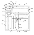
図2において、201は基板(ガラス基板または石英基板を含む)、202は酸化珪素膜でなる下地膜、203は非晶質珪素膜、204はバッファ層となる酸化珪素膜である。また、205はレジストマスクであり、触媒元素を添加する領域のみを除去しておく。レジストマスクの露光はエキシマレーザーを用いた露光法や電子ビームを用いた露光法などを用いることが好ましい。
【0070】
これらの露光法は極めて微細なパターン形成が可能となるので 0.01 〜1.0 μm(代表的には 0.1〜0.35μm)のスリット幅で触媒元素の添加領域を形成することができる。また、電子ビーム等で直接レジストパターンを描画すれば、添加領域の形状の自由度も大幅に広がる。
【0071】
そして、図2の左の図に示す様に、非晶質珪素膜203中にイオンプロファイル207のピーク値がくる様にしてイオンを添加する。そのため、非晶質珪素膜203中には所定の濃度(好ましくは 3×10¹⁹〜 1.5×10²¹atoms/cm3 )で触媒元素が添加された領域206が形成される。
【0072】
なお、イオンの添加方法は、質量分離を行うイオン注入法以外に質量分離を行わないプラズマドーピング法(イオンドーピング等)によることもできるが、触媒元素のみを添加できる点でイオン注入法の方が有利である。
【0073】
また、図2に示す構成ではバッファ層204で非晶質珪素膜203を覆い、バッファ層204を通過した触媒元素のみを利用する。そのため、イオン注入時のイオンの衝突によるダメージが非晶質珪素膜203に対して直接届かないという利点が得られる。
【0074】
また、イオンプロファイル207のピーク値付近のみを利用するので、イオン注入の条件を最適化することで触媒元素の添加量を再現性良く制御できる。即ち、横成長領域の成長距離は添加する触媒元素の濃度によって変化するため、イオン注入法を用いることで横方向への成長距離を容易に制御することができる。
【0075】
この事は、所望の位置に所望の広さで横成長領域を形成することができることを意味している。即ち、TFTサイズ(チャネル形成領域の長さ)を考慮して必要十分な広さの横成長領域を形成することができる。
【0076】
(第2の構成の概要)
上述の手段によれば、図3(A)に示す様に、同一基板上において異なる成長距離の横成長領域を形成することが可能となる。図3(A)において、301は図1に示す様なシステムディスプレイの簡略図であり、302は画素マトリクス回路、303、304はドライバー回路、305はロジック回路である。
【0077】
画素マトリクス回路302を構成するTFT(画素TFT)は高耐圧特性を要求されるため、チャネル長(ゲイト長)を長くする(代表的には2〜20μm)などの工夫が施される。従って、306に示される様に横成長領域の成長距離X1 は画素TFTの活性層307の長さ以上とする様に設計する。この時、添加領域308に添加される触媒元素の濃度n1 は、添加濃度と成長量の関係を実験的に求めて調節すれば良い。
【0078】
一方、ロジック回路305を構成するTFT(ロジックTFT)は高速動作特性を要求されるため、チャネル長を短くする(代表的には0.25〜0.7 μm)などの工夫が施される。従って、309に示される様に横成長領域の成長距離X2 はロジックTFTの活性層310の長さに合わせて調節すれば良い。なお、この時、添加領域311の触媒元素の濃度をn2 とする。
【0079】
以上の様に、図3(A)の場合には異なる成長距離X1 、X2 を有する横成長領域が同一基板上に存在する。この場合、X1 >X2 である。また、成長距離X1 、X2 を有する横成長領域はそれぞれ異なる触媒元素濃度n1 、n2 の添加領域から成長した領域である。この場合、n1 >n2 の関係がある。即ち、この構成は添加領域に存在する触媒元素の濃度が高いほど横成長領域の成長距離が長くなるという現象を利用したものである。
【0080】
この様に、同一形状の添加領域であってもそこに添加される触媒元素の濃度を調節することで所望の幅の横成長領域を形成できる。即ち、回路が要求する特性に応じてチャネル長を変えた場合に、チャネル長に合わせて異なる成長距離を有する横成長領域を形成する点が、本発明の第2の構成の要点である。
【0081】
なお、チャネル長に合わせて成長距離を異ならせるため、チャネル長と横成長領域の成長距離との間には何らかの相関関係がある。例えば、チャネル形成領域が完全に横成長領域内に入る様に、チャネル長(またはチャネル幅)に数μmの固定マージンを加えた距離が成長距離となる様に触媒元素濃度を調節したり、チャネル長(またはチャネル幅)の2倍の距離が成長距離となる様に調節したりすることも考えられる。この相関関係は成長距離の誤差や活性層形成時のパターニング精度によって変わりうるので一概には言えないが、触媒元素の添加濃度を決定する上で重要である。
【0082】
また、発明の第2の構成の利点は、特に微細なTFTを作製する領域において必要以上に横成長領域を大きくしないで済む点にある。
【0083】
例えば、309に示されるロジックTFTの活性層を構成する場合、必要以上に横成長領域の幅を長くしてしまうと、他の異なる機能を有する回路にまで横成長領域が広がってしまい、前述の様にTFT特性のバラツキを招く原因となる。この様にしてTFT特性のバラツキが引き起こされると、非常に高い周波数で駆動する回路や、差動アンプやオペアンプに様に極めてシビアにTFT特性の均一性を求められる構成を含む回路を構成する場合に弊害を生じる。
【0084】
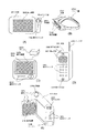
ここでロジック回路の一例としてオペアンプに本発明の第2の構成を適用した例を図4を用いて説明する。図4(A)に示すのはTr1〜Tr8の8つのTFTを用いて構成されるオペアンプ回路の一例であり、図4(B)に示す様な回路図で表される。
【0085】
図4(A)において、401は前述の特異な結晶構造体で構成される活性層であり、Tr1〜Tr8を構成している。402は第1の配線層であり、TFTのゲイト絶縁膜や出力用の引き出し配線として利用している(なお、図中において同じ柄の配線は全て同一の配線層である)。また、403は第2の配線層であり、入力端子、電源端子(VDD端子)、GND端子、バイアス端子とTFTとを接続している。そして、404〜407がイオン注入法により触媒元素が添加された領域である。
【0086】
この時、図4(A)(または図4(B))に示すオペアンプはTr4およびTr8(またはTr6およびTr7)でなる差動増幅回路を基本として構成される。差動増幅回路は温度変化や電源電圧の変化があっても2つのTFTに同時に作用するため出力に影響を及ぼさない特徴がある。しかし、そのためには2つのTFTの特性が揃っていることが前提となる。
【0087】
そのため、例えばTr4とTr8を構成する活性層が触媒元素の添加領域から等しい距離の位置に配置される様に、Tr4には添加領域405、Tr8には添加領域407を配置する様な工夫が施されている。また、Tr6とTr7を構成する活性層に関しても同様の処置が施されている。
【0088】
なお、TFTで構成されるロジック回路は高周波動作を必要とするため、ゲイト長が0.25〜0.7 μm程度にまで微細化される。従って、図4(A)に示すオペアンプの回路寸法は 5〜20μm程度の大きさとなる。
【0089】
ところが、特開平8-78329 号公報記載の技術では触媒元素の添加領域が少なくとも20μmの幅を持つため、TFTとTFTとの隙間に添加領域を形成することは不可能である。また、横成長領域が必要以上に大きくなるため、上述の様なTFT特性を揃える様な工夫は不可能である。即ち、この図4(A)に示す構成は、本発明の第2の構成を用いることで成就することが可能なのである。
【0090】
また、図4(A)に示す様な微細な回路では横成長領域が大きくなりすぎると、周囲の横成長領域にまで干渉するため好ましくない。本発明の第2の構成では触媒元素の濃度を調節することで容易に横成長領域の成長距離を制御することが可能なので、微細な配置構成で添加領域を形成する場合においても、横成長領域の相互干渉を最低限に抑えることができる。
【0091】
勿論、画素マトリクス回路を構成する画素TFTの様にゲイト長が長い場合には、触媒元素の添加量を高くして横成長領域の成長距離を長くすることができる。また、TFT特性のバラツキを問題としない様な微細な回路の場合には、触媒元素の濃度を高くして広い横成長領域を形成し、一括で複数の活性層を構成することも可能である。
【0092】
【実施例2】
実施例1の図1で示した様なシステムディスプレイにおいて、ロジック回路105やドライバー回路103、104を構成する回路は、Nチャネル型TFTとP型チャネルTFTとを相補的に組み合わせたCMOS回路(インバータ回路)を基本構成としている。そして、これらの駆動系回路は 0.1〜2 GHz、場合によっては2GHz以上の極めて高い駆動周波数を必要とすることがあるため、ゲイト長は0.25〜0.7 μmにまで微細化される。
【0093】
また、画素マトリクス回路102は液晶表示装置の場合には高い耐圧特性を要求されるのでゲイト長は 2〜20μm程度の範囲で形成される。なお、場合によっては実質的にTFTを直列に接続した構成のマルチゲイト型TFTを用いることもある。
【0094】
本実施例では、同一基板上において回路が要求する特性に応じて異なるデバイスサイズのTFTを配置するに際し、それぞれのデバイスサイズに対応して異なる成長距離を有する横成長領域を形成し、その領域を利用して特異な結晶構造体でで構成されるTFTを作製する例を示す。ここでは一例として、同一基板上にCMOS回路と画素TFTとを作製する場合の作製工程例を図5〜図7を用いて説明する。
【0095】
図5(A)において、501は石英基板である。石英基板の代わりに表面に0.5 〜5 μmの厚さの絶縁膜を成膜したセラミックス基板、単結晶シリコンウェハーおよび多結晶シリコンウェハーを用いることもできる。なお、ここでいうシリコンウェハーは太陽電池に使用される様な低級グレードのウェハーで十分であり、石英よりも安価であるので反射型表示装置やICチップの様に透過性基板を用いる必要のない用途に用いる場合に有効である。
【0096】
502は非晶質シリコン膜であり、最終的な膜厚(熱酸化後の膜減りを考慮した膜厚)が10〜75nm(好ましくは15〜45nm)となる様に調節する。成膜は減圧熱CVD法またはプラズマCVD法によれば良い。また、503は非晶質シリコン膜502を酸化して得られる 5〜50nm程度の薄い酸化膜である。
【0097】
次に、触媒元素の添加領域を選択するレジストマスク504を形成する。レジストマスク504は、図2に示した様に0.01〜1 μmの幅を有するコンタクトホールを有している。このコンタクトホールは、後にCMOS回路を構成するTFTの活性層となる横成長領域を形成するためのものである。
【0098】
そして、非晶質シリコン膜の結晶化を助長する触媒元素としてニッケル(Ni)をイオン注入法により添加する。なお、触媒元素としてはニッケル以外にも、コバルト(Co)、鉄(Fe)、錫(Sn)、鉛(Pb)、パラジウム(Pd)、白金(Pt)、銅(Cu)、金(Au)等を用いることができる。
【0099】
この時、添加領域505には、後に成長距離X1 の横成長領域を形成できる様に濃度n1 のニッケルが添加される。n1 の値は後の熱結晶化工程の条件によっても異なるので実施者が実験的に決定すれば良い。(図5(A))
【0100】
次に、レジストマスク504を除去した後、再びレジストマスク506を形成する。このレジストマスク506は、後に画素TFTの活性層となる横成長領域を形成するためのものである。そして、再びイオン注入法によりニッケルを添加する。この時、添加領域507には、後に成長距離X2 の横成長領域を形成できる様に濃度n2 のニッケルが添加される。n2 の値は前述と同様に実施者が実験的に決定すれば良い。(図5(B))
【0101】
以上の様に、同一基板上の少なくとも1ヶ所は他の添加領域とは異なる濃度で触媒元素が添加されることになる。
【0102】
次に、触媒元素の添加工程が終了したら、不活性雰囲気または水素を含む雰囲気中において 500〜700 ℃、代表的には 550〜650 ℃の温度で 4〜8 時間の加熱処理を加えて非晶質シリコン膜502の結晶化を行う。結晶化は膜中のニッケル(またはニッケルシリサイド)が核となって進行する。(図5(C))
【0103】
非晶質シリコン膜502の結晶化はニッケルを添加した添加領域505、507から優先的に進行し、基板501と概略平行に成長した横成長領域508、509が形成される。前述の様に、添加領域505はニッケル濃度をn1 とし、添加領域507はニッケル濃度をn2 (n1 >n2 )としているので、横成長領域508(成長距離X1 )と横成長領域509(成長距離X2 )との間にはX1 >X2 の関係がある。即ち、同一基板上の少なくとも1ヶ所は他の横成長領域とは異なる成長距離を有する横成長領域が形成されることになる。
【0104】
本発明ではこの横成長領域508、509のみを結晶シリコン膜として利用する。即ち、添加領域の配置によって横成長領域を形成する位置を自由に設計することができるため、従来のポリシリコン膜の様に結晶粒界がTFT特性に影響する様なことがない。
【0105】
結晶化のための加熱処理が終了したら、パターニングを行い横成長領域のみでなる島状半導体層(活性層)510〜512を形成する。ここで510はCMOS回路を構成するNチャネル型TFTの活性層、511はCMOS回路を構成するPチャネル型TFTの活性層、512は画素TFTを構成するNチャネル型TFTの活性層である。(図5(D))
【0106】
なお、図5(D)に示す状態となっても横成長領域508、509が存在した痕跡が幾つか残る。例えば、添加領域505、507はシリサイド化して優先的に消失するため添加領域の存在した直下の下地(この場合は石英)には凹部が形成される。また、横成長領域の端部(結晶化の終点)にも触媒元素が偏析するので、この領域にも下地に凹部が形成される。さらに、添加領域505、507は触媒元素の添加濃度が異なるので、棒状または偏平棒状結晶の結晶性や形状も添加濃度に応じて異なると考えられる。
【0107】
横成長領域でなる結晶シリコン膜で構成される活性層510〜512を形成したら、活性層510〜512上に酸化珪素膜でなるゲイト絶縁膜513を成膜する。この時、ゲイト絶縁膜513の膜厚はCMOS回路側(514で示される)と画素TFT側(515で示される)とで異なるものとすることが望ましい。
【0108】
なぜならば、CMOS回路は高周波駆動用にゲイト長の短いTFTとなるのでドレイン耐圧が低いことを考慮して動作電圧を低くする必要がある。そのため、ゲイト絶縁膜の膜厚を 2nm以上80nm未満(代表的には50nm)としてしきい値電圧を下げ、動作電圧の低下を図ることが好ましい。また、画素TFTは動作電圧が高いのでゲイト絶縁膜の膜厚を80nm以上250 nm以下(代表的には120 nm)としてドレイン耐圧を高くする工夫を施すことが有効である。
【0109】
同一基板上に異なる膜厚のゲイト絶縁膜を形成するには、マスクを用いて選択的に積層したり、LOCOS 法の如き選択酸化法を用いて特定の活性層に熱酸化膜を形成し、膜厚を厚くするなどの方法を用いれば良い。また、最終的に必要とするゲイト絶縁膜の厚さが50nm以下となる場合、後の熱酸化工程で得られる熱酸化膜のみをゲイト絶縁膜として利用することもできる。
【0110】
次に、図5(E)に示す様に触媒元素(ニッケル)をゲッタリング除去するための加熱処理(触媒元素のゲッタリングプロセス)を行う。この加熱処理はハロゲン元素による金属元素のゲッタリング効果を利用するものである。
【0111】
ハロゲン元素によるゲッタリング効果を十分に得るためには、上記加熱処理を700 ℃を越える温度で行なうことが好ましい。そのため、本実施例ではこの加熱処理を700 ℃を超える温度で行い、好ましくは800 〜1000℃(代表的には950 ℃)とし、処理時間は 0.1〜 6時間、代表的には 0.5〜 1時間とする。
【0112】
なお、ここでは酸素(O2 )雰囲気中に対して塩化水素(HCl)を0.5 〜10体積%(本実施例では3体積%)の濃度で含有させた雰囲気中において、950 ℃、30分の加熱処理を行う例を示す。HCl濃度を上記濃度以上とすると、活性層209の表面に膜厚と同程度の凹凸が生じてしまうため好ましくない。
【0113】
また、上述の酸化性雰囲気中に高濃度の窒素(N2 )を混ぜた雰囲気とすることで結晶シリコン膜の酸化速度を低下させることができる。熱酸化反応を必要以上に進ませずにゲッタリング時間を増やす場合に有効な手段である。
【0114】
また、ハロゲン元素を含む化合物してHClガスを用いる例を示したが、それ以外のガスとして、代表的にはHF、NF3 、HBr、Cl2 、ClF3 、BCl3 、F2 、Br2 等のハロゲンを含む化合物から選ばれた一種または複数種のものを用いることが出来る。
【0115】
この工程においては横成長領域508、509中に添加されたニッケルが塩素の作用によりゲッタリングされ、揮発性の塩化ニッケルとなって大気中へ離脱して除去されると考えられる。なお、シリコン膜上の酸化膜503やゲッタリングプロセス中に形成される熱酸化膜は非常に薄いので塩化ニッケルの離脱を妨げるブロッキング層とはならない。
【0116】
そして、この触媒元素のゲッタリングプロセスにより横成長領域508、509中のニッケルの濃度は 1×10¹⁷atoms/cm3 以下(好ましくはスピン密度以下)にまで低減される。なお、本明細書における不純物濃度はSIMS分析で得られた計測値の最小値で定義される。なお、同様のSIMS分析により横成長領域508、509中にはゲッタリング処理に使用したハロゲン元素が 1×10¹⁵〜 1×10²⁰atoms/cm3 の濃度で残存することも確認されている。
【0117】
また、上記加熱処理により活性層510〜512とゲイト絶縁膜513の界面では熱酸化反応が進行し、形成された熱酸化膜(図示せず)の分だけゲイト絶縁膜513の全膜厚は増加する。そのため、熱酸化膜の形成分に比例して活性層510〜512は薄膜化される。活性層の薄膜化はTFTのオフ電流の低減、電界効果移動度の向上などの効果を促進する。また、その際、活性層510〜512と加熱処理によって形成される熱酸化膜との間に前述のハロゲン元素が高濃度に分布することがSIMS分析によって確かめられている。
【0118】
さらに、上記ハロゲン雰囲気における加熱処理を施した後に、窒素雰囲気中で950 ℃ 1時間程度の加熱処理を行なうことで、ゲイト絶縁膜513の膜質の向上と共に、極めて良好な半導体/絶縁膜界面が実現される。
【0119】
以上の様な工程を経て形成された結晶シリコン膜は実施例1に述べた様な特異な結晶構造体となっている。即ち、実施例1に示した様な極めて優れた電気特性を有するTFTを実現することが可能となる。
【0120】
次に、0.2wt%のスカンジウムを含有したアルミニウム膜(図示せず)を成膜し、後のゲイト電極の原型となる電極パターンを形成する。そして、そのパターンの表面を陽極酸化することで、ゲイト電極516〜518、陽極酸化膜519〜521を形成する。(図6(A))
【0121】
この時、ゲイト電極516〜518の線幅(ゲイト長)は回路が要求する特性を鑑みて決定すれば良い。高周波駆動を要求するロジック回路等であれば0.25〜0.7 μmとすれば良いし、高耐圧特性を要求する画素マトリクス回路等であれば
2〜20μmとすれば良い。
【0122】
次に、ゲイト電極516〜518をマスクとして自己整合的にゲイト絶縁膜513のエッチングを行う。エッチングはCHF3 ガスを用いたドライエッチング法で行えば良い。この工程により、ゲイト電極の直下のみに残存するゲイト絶縁膜522〜524が形成される。
【0123】
次に、Pチャネル型TFTとなる領域を覆ってレジストマスク525を形成した後、N型を付与する不純物イオンの添加を行う。不純物イオンの添加はイオン注入法やプラズマドーピング法によれば良い。また、この時の濃度(n- で表す)は後にLDD領域の濃度( 1×10¹⁸〜 1×10¹⁹atoms/cm3 程度)となるので、予め最適値を実験的に求めて精密な制御を行う必要がある。こうして、n- 領域526〜529が形成される。(図6(B))
【0124】
n- 領域526〜529を形成したら、レジストマスク525を除去して、今度はNチャネル型TFTを覆ってレジストマスク530を形成する。そして、P型を付与する不純物イオンの添加を行い、p- 領域531、532を形成する。このp- 領域531、532も後にLDD領域の濃度( 5×10¹⁸〜 5×10¹⁹atoms/cm3 程度)となるので精密な制御を行う必要がある。(図6(C))
【0125】
以上の様にしてn- 領域526〜529、p- 領域531、532を形成したら、レジストマスク530を除去する。そして、図示しない酸化珪素膜を 0.5〜2 μmの厚さに成膜し、エッチバック法によりサイドウォール533〜535を形成する。(図6(D))
【0126】
次に、再びPチャネル型TFTを覆ってレジストマスク536を形成し、N型を付与する不純物イオンの添加工程を行う。今回は前述の添加濃度であるn- よりも高い濃度(n+ で表す)で添加する。この濃度はソース/ドレイン領域のシート抵抗が500 Ω以下(好ましくは300 Ω以下)となる様に調節する。
【0127】
この工程によりCMOS回路を構成するNチャネル型TFTのソース領域537、ドレイン領域538が形成され、サイドウォールの影になって濃度の変化しなかった領域539が低濃度不純物領域(特にドレイン領域側はLDD領域と呼ばれる)となる。また、ゲイト電極の直下は真性または実質的に真性なチャネル形成領域540となる。また、同時に画素TFTとなるNチャネル型TFTのソース領域541、ドレイン領域542、低濃度不純物領域543、チャネル形成領域544が形成される。(図6(E))
【0128】
次に、レジストマスク536を除去し、Nチャネル型TFTを覆ってレジストマスク545を形成する。そして、P型を付与する不純物イオンを1度目よりも高い濃度(p+ で表す)で添加することにより、CMOS回路を構成するPチャネル型TFTのソース領域546、ドレイン領域547、低濃度不純物領域548、チャネル形成領域549を形成する。(図7(A))
【0129】
以上の様にして全ての活性層が完成する。こうして全ての不純物イオンの添加工程が終了したら、レジストマスク545を除去した後、ファーネスアニール、レーザーアニール、ランプアニール等の加熱処理により不純物イオンの活性化を行う。なお、活性層が受けたイオン注入時のダメージは同時に回復される。
【0130】
次に、チタン(Ti)膜550を20〜50nmの厚さに成膜して、ランプアニールによる加熱処理を行う。この時、チタン膜550と接触していたシリコン膜はシリサイド化し、ソース/ドレイン領域にはチタンシリサイド551〜553が形成される。なお、チタンの代わりにタングステン(W)、タンタル(Ta)、モリブデン(Mo)等を用いることもできる。
【0131】
シリサイド化を終えたら、チタン膜550をパターニングしてソース/ドレイン領域上に島状パターン554〜556を形成する。この島状パターン554〜556は、後にソース/ドレイン領域と配線とを接続するコンタクトホールを形成する際にチタンシリサイド551〜553が無くなってしまうのを防ぐためのパターンである。勿論、コンタクトホールを形成する層間絶縁膜とチタンシリサイドとの選択比が大きければ島状パターン554〜556を省略することは可能である。
【0132】
次に、第1の層間絶縁膜557として酸化珪素膜を 0.3〜1 μmの厚さに成膜し、コンタクトホールを形成してソース配線558〜560、ドレイン配線561、562を形成する。こうして図7(C)に示す状態が得られる。なお、第1の層間絶縁膜557として有機性樹脂膜を用いることもできる。
【0133】
図7(C)に示す状態が得られたら、有機性樹脂膜でなる第2の層間絶縁膜563を 0.5〜3 μmの厚さに形成する。有機性樹脂膜としてはポリイミド、アクリル、ポリアミド、ポリイミドアミド等が用いられる。有機性樹脂膜の利点は、▲1▼成膜方法が簡単である点、▲2▼容易に膜厚を厚くできる点、▲3▼比誘電率が低いので寄生容量を低減できる点、▲4▼平坦性に優れている点などが挙げられる。
【0134】
そして、層間絶縁膜563上の画素TFTの上方に遮光性を有する膜でなるブラックマスク564を 100nmの厚さに形成する。実際には画素マトリクス回路の配線上やTFT上の様に遮光の必要性のある場所に設ける。本実施例ではブラックマスクとしてチタン膜を用いるが、黒色顔料を含む樹脂膜等でも良い。
【0135】
ブラックマスク564を形成したら、第3の層間絶縁膜565として再び有機性樹脂膜を 0.1〜0.3 μmの厚さに形成する。そして、第2の層間絶縁膜563および第3の層間絶縁膜565にコンタクトホールを形成し、画素電極566を
120nmの厚さに形成する。(図7(D))
【0136】
なお、作製する表示装置が透過型表示装置であれば画素電極566として透明導電膜(例えばITO膜)を用いれば良く、反射型表示装置であれば画素電極566として反射性導電膜(例えばアルミニウム膜)を用いれば良い。
【0137】
また、この時ブラックマスク564と画素電極566が重畳する領域では補助容量が形成される。この補助容量は画素電極にかかる電圧を一定に保つための蓄積容量として機能する。そのため、本実施例では補助容量を構成する絶縁体として第3の層間絶縁膜565を用いるが、第3の層間絶縁膜565をさらに比誘電率の高い酸化珪素膜や窒化珪素膜とすれば補助容量のキャパシティを増すことが可能である。
【0138】
最後に、基板全体を水素雰囲気で加熱し、素子全体の水素化を行うことで膜中(特に活性層中)のダングリングボンド(未結合手)を補償する。以上の工程を経て同一基板上にCMOS回路および画素TFTを作製することができる。
【0139】
【実施例3】
本実施例では図1に示す様なシステムディスプレイにおいて画素マトリクス回路を構成する画素領域の構成に関する一例を示す。まず、図14(A)に画素領域の上面図を示す。
【0140】
図14(A)において1401、1402は活性層、1403、1404はゲイト線、1405、1406はソース線である。実際には複数本のソース線とゲイト配線とが直交する様に配置され、ソース線とゲイト線とで囲まれた複数のマトリクス状に配置された領域が図1における画素領域110として機能する。
【0141】
また、活性層1402の上方では3箇所においてゲイト線1404が重畳する。即ち、本実施例の構成では3つの画素TFTを直列に接続したのと同様の構造となるトリプルゲイト型TFTが構成される。
【0142】
また、ゲイト配線1405、1406を活性層1401、1402よりも下層に配置して逆スタガ型TFTの様な構造とすることも可能である。その場合、シリコン薄膜の作製過程で行われる図5(E)の様な加熱処理にも耐えうる様に、ゲイト電極としてはポリシリコン膜の様な耐熱性の高い材料を用いるのが好ましい。
【0143】
次に、1407は活性層1402(ソース領域)とソース線1405とのコンタクト部、1408は活性層1402(ドレイン領域)とドレイン配線1409とのコンタクト部、1410はドレイン配線1409と画素電極1411とのコンタクト部である。
【0144】
1412の斜線で示される領域はブラックマスクであり、活性層1401、1402、ゲイト配線1403、1404、ソース線1405、1406上を遮蔽する様にして形成される。また、ブラックマスク1412は1413で示される領域においてドレイン配線1409と重畳し、ドレイン配線1409との間に補助容量を形成する。
【0145】
また、ブラックマスク1412上には第3の層間絶縁膜を介して画素電極1411が配置されている。画素電極1411はその淵部分が必ずブラックマスク1412によって遮光される構成とし、ブラックマスク1412と重畳しない1414で示される領域が画像を形成する画像表示領域となる。なお、実際には、画素電極1411の上には対向基板、対向電極、液晶層が配置されて図1に示す液晶セル112を構成する。
【0146】
次に、図14(A)をA−A’で切断した断面図を図14(B)に示す。なお、基本的なトランジスタ構造については実施例2で詳細な説明を行ったので、ここでは図14(A)との対応関係についてのみ記載する。
【0147】
図14(B)において、1415は石英基板、1416、1417はそれぞれ図14(A)における活性層1402のソース領域およびドレイン領域である。また、1418はゲイト電極であり、図14(A)におけるゲイト配線1404の相当する。なお、図面上では3つのゲイト電極が並んでいる様に見えるが、実際には図14(A)の様に同一配線で構成されている。
【0148】
次に、第1の層間絶縁膜1419上にソース配線1420(図14(A)の1405に相当する)、ドレイン配線1421(図14(A)の1409の相当する)が配置される。なお、1422はソース線1420と隣接する隣のソース線である。
【0149】
そして、ソース配線1420、ドレイン配線1421を覆って酸化珪素膜または窒化珪素膜あるいはその積層膜でなる第2の層間絶縁膜1423を50〜200nm の厚さに形成し、その上に有機性樹脂膜でなる第3の層間絶縁膜1424を形成する。さらに、第3の層間絶縁膜1424上にはブラックマスク1425(図14(A)の1412の相当する)が配置される。
【0150】
この時、ブラックマスク1425を形成する前に第3の層間絶縁膜1424は1426で示される領域において除去される。従って、1426で示される領域では、ドレイン配線1421と第2の層間絶縁膜1423とブラックマスク1425との積層構造でなる補助容量1427が形成される。この補助容量1427は図14(A)において1411で示される補助容量に相当する。
【0151】
補助容量1427を図14(B)に示す様な構成とすると、補助容量のキャパシタンス(容量)が第2の層間絶縁膜1423で決まるので、比誘電率の高い材料を用いること或いは膜厚を薄くすることで容量を稼ぐことができる。ただし、補助容量1427を形成するには1426で示される領域において第2の層間絶縁膜1423のみを残して第3の層間絶縁膜1424を除去しなくてはならないので、第2、第3の層間絶縁膜はそれぞれエッチングの選択性が採れなくてはならない。その様な意味で、第2の層間絶縁膜1423としては酸化珪素膜または酸化珪素膜と窒化珪素膜との積層膜が有効である。
【0152】
次に、1428は有機性樹脂膜でなる第4の層間絶縁膜であり、その上には画素電極1429が形成される。この時、画素電極1429はドレイン配線1421を介してドレイン領域1417と電気的に接続する。このため、補助容量1427は画素電極1429に対して直列に接続された容量と見なせる。
【0153】
また、1430で示される基板は対向電極1431を成膜した対向基板であって、アクティブマトリクス基板1415と対向基板1430とを貼り合わせることで液晶層1432を挟持し、図1における液晶セル112が形成される。
【0154】
【実施例4】
本実施例では実施例2と異なる構成を有するCMOS回路を構成する場合の例について図15(A)、(B)を用いて説明する。なお、図15(A)、(B)は基本的な部分は全て実施例2で説明したCMOS回路と同一構造であるので、符号は実施例2と同一のものを適宜利用する。
【0155】
まず、図15(A)は実施例2で示したCMOS回路において、ゲイト電極1501、1502として一導電性を付与したシリコン薄膜(ポリシリコン膜)を利用したシリコンゲイト型TFTでCMOS回路を構成する例である。なお、Nチャネル型TFTとPチャネル型TFTとでゲイト電極の導電性を異なるものとする(N型またはP型)デュアルゲイト型TFTとすることもできる。
【0156】
この様なシリコンゲイト構造とすると、チタンシリサイド551、552の形成と同時にゲイト電極1501、1502の上部にもチタンシリサイド1503、1504が形成される。そのため、ゲイト電極とゲイト電極に接続する接続配線とのオーミックコンタクトをより良好なものとすることができる。
【0157】
また、図15(B)は実施例2で示したCMOS回路において、サイドウォール533、534およびチタンでなる島状パターン554、555を形成しない場合の例である。この構成では、ゲイト絶縁膜1505、1506の端部(ゲイト電極516、517よりも外側に延在した部分)の幅で低濃度不純物領域539、548の長さが決定される。また、チタンシリサイド1507、1508とソース配線558、559、561とが直接コンタクトする様な構造となる。
【0158】
実施例2におけるサイドウォール533、534の主だった役割は、低濃度不純物領域539、548の長さおよび添加濃度の決定である。しかし、図15(B)に示す構成では本発明者らによる特開平7-135318号公報記載の技術を利用しているため、サイドウォールを利用しない構成とすることができる。
【0159】
また、実施例2における島状パターン554、555の主だった役割は、ソース/ドレイン領域に形成されたチタンシリサイド551、552と、ソース/ドレイン配線とのオーミックコンタクトを確保することである。この場合、島状パターン554、555は、層間絶縁膜557にコンタクトホールを形成する際にチタンシリサイド551、552が除去されてしまうことを防ぐ保護層としても機能している。
【0160】
本実施例ではコンタクトホール形成をドライエッチング法で行い、層間絶縁膜557とチタンシリサイド551、552との選択比を高めることで、保護層として島状パターン554、555を設ける必要のない構成としている。
【0161】
以上の様にしてサイドウォール533、544および島状パターン554、555を形成する工程を簡略化することで、スループットの向上、歩留りの向上、製造コストの低減が期待できる。
【0162】
【実施例5】
本発明を実施するにあたって、発明の第1の構成で説明したシリコン薄膜が必要であることは既に述べた。本実施例では、実施例2とは異なる手段で結晶化したシリコン薄膜を本発明に用いる場合の例を示す。
【0163】
図5において、図5(C)に示す状態(結晶化のための加熱処理が終了した段階)を得たら、結晶シリコン膜表面の酸化膜503を除去する。酸化膜503を除去したら、KrF(波長248nm )、XeCl(波長308nm )等を励起ガスとして利用したエキシマレーザーによるアニールを行う。なお、このレーザーアニール工程はシリコン薄膜を島状パターンに加工する前でも後でもどちらで行っても構わない。
【0164】
上記レーザーアニールによって、結晶シリコン薄膜に僅かに残存した非晶質成分の結晶化及び結晶シリコンの結晶性の著しい改善が行われる。この様にして得られたシリコン薄膜を用いても、本発明のシステムディスプレイを形成しうる。本実施例の利点は、システムディスプレイを安価なガラス基板上に形成できる点である。即ち、製造コストの低減を図ることができる。
【0165】
ただし、本発明を実施する上で最も望ましい形態は実施例1に示したシリコン薄膜を活用したTFTを用いることであり、本実施例は基板としてガラス基板等の低耐熱性基板を使用する必要性が生じた場合のみに使用するのが好ましい。
【0166】
また、実施例1に示した工程と本実施例の工程とを組み合わせても良い。即ち、レーザーアニール工程の後に触媒元素のゲッタリングプロセスを行う構成としても構わない。その場合、さらに高い結晶性のシリコン薄膜を形成しうる。
【0167】
【実施例6】
本発明は図2を用いて説明した様なイオン注入法だけでなく、他の実施形態としてレジストマスクを使用しないで触媒元素を直接的に非晶質シリコン膜中へと添加することもできる。
【0168】
そのための手段としては、FIB(Focussed Ion Beam )法等の様に微細スポットのみにイオンを照射できる様な技術がある。この様な技術によれば触媒元素を含む集束イオンビームによって直接的にパターンが描画され、所望の位置に所望の形状で触媒元素の添加領域を形成できる。
【0169】
本実施例によればレジストマスクを形成する工程やパターニング工程を簡略化することができるので、製造コストの低減および製造歩留りの向上を図ることが可能である。
【0170】
【実施例7】
本実施例では実施例2に示した層間絶縁膜(第1〜第3まで)の組み合わせについての幾つかの例を説明する。
【0171】
まず、図7(D)においてアルミニウムを主成分とする配線558〜562の下地となる第1の層間絶縁膜557およびチタン膜でなるブラックマスク564の下地となる第2の層間絶縁膜565としてはポリイミドを用いる。そして、画素電極566の下地となる第3の層間絶縁膜565はアクリルを用いる。
【0172】
本発明者らの実験条件では配線558〜562とブラックマスク564の成膜温度( 300℃程度)がアクリルの耐熱温度( 200℃程度)よりも若干高いため、下地としては成膜温度に耐えうるポリイミド(耐熱温度は 350〜400 ℃程度)を用いることが好ましい。また、画素電極566は室温成膜なので下地として耐熱性の低いアクリルを使用することができる。ただしこの構成は、画素電極566がITO等の様に成膜温度の低い材料(アクリルの耐熱温度以下で成膜できる材料)である場合に限る。
【0173】
この様な構成とした時、次の様な利点を得ることができる。
(1)アクリルは感光性であるためレジストマスクを使用しないで直接パターニングできるため、製造工程を簡略化できる。
(2)アクリルはポリイミドよりも安価なので製造コストを低減できる。
(3)ITOとポリイミドとの間の密着性よりもITOとアクリルとの間の密着性の方が良好である。
(4)アクリルの方が平坦性に優れるため、画素電極上にかかる電界を均一なものとすることができる。
【0174】
また、別の例として全ての層間絶縁膜をポリイミドで形成することもできるし、全ての層間絶縁膜をアクリルで形成することもできる。ただし、全ての層間絶縁膜をアクリルで形成する場合、アクリルを成膜した後の工程は全てアクリルの耐熱温度以下で行われることが条件である。
【0175】
【実施例8】
本発明はあらゆる半導体装置に対して適用可能であり、絶縁表面を有する基板上においてTFTを用いて回路を構成した半導体装置であれば全て適用範囲に入る。その様な半導体装置は、ICやVLSIの様にロジック回路のみとして機能する場合もあるし、アクティブマトリクス型電気光学装置の様に表示ディスプレイとして機能する場合もある。
【0176】
特に、アクティブマトリクス型電気光学装置としては、図1に示した様なロジック回路内蔵型のシステムディスプレイを用いてアクティブマトリクス型液晶表示装置、アクティブマトリクス型EL表示装置、アクティブマトリクス型EC表示装置などに適用することができる。
【0177】
また、これらの様なアクティブマトリクス型の表示装置には大別して透過型表示装置と反射型表示装置とがある。例えば、透過型液晶表示装置はアクティブマトリクス基板(TFTを配置する側の基板)の裏側にバックライトを配設し、表示装置を透過する光を見ることで画像を認識するものである。また、反射型液晶表示装置はアクティブマトリクス基板の表面側から入射した光をアクティブマトリクス基板に配置される画素電極で反射し、その反射光を見ることで画像を認識するものである。
【0178】
透過型表示装置と反射型表示装置とでTFT構造に大きな差異がないが、画素電極を形成する材料が異なる点に特徴がある。例えば、透過型表示装置を作製する場合、図14(A)における画素電極1411としてITO等の透明電極を使用すれば良い。また、反射型表示装置とする場合には、画素電極1411として反射効率の高い不透明電極を使用すれば良い。
【0179】
この様に、多少TFT構造を変化させれば、本発明は透過型表示装置にも反射型表示装置にも適用できる。特に、反射型表示装置は開口率を問題としないため、透過型表示装置に比べて設計自由度が広がるという利点を有する。例えば透過型液晶表示装置において画素領域は殆ど画像表示領域1414の様に光を透過する窓部分で構成されているが、反射型液晶表示装置の場合にはその様な画像表示領域の裏側に別の回路を形成することが可能であるため集積度をより高めることができる。
【0180】
【実施例9】
本実施例では、本発明を適用しうる半導体装置の一例として実施例8で示した様な電気光学装置を用いた応用製品について図16を用いて説明する。
【0181】
本発明を利用した半導体装置としては(デジタル)ビデオカメラ、(デジタル)スチルカメラ、ヘッドマウントディスプレイ、カーナビゲーション、パーソナルコンピュータ、携帯情報端末(モバイルコンピュータ、携帯電話等)などが挙げられる。
【0182】
図16(A)はモバイルコンピュータ(モービルコンピュータ)であり、本体2001、カメラ部2002、受像部2003、操作スイッチ2004、表示装置2005で構成される。本発明を表示装置2005に適用して表示コントロール回路や演算回路等を組み込むことでカード型モバイルコンピュータを実現しうる。
【0183】
図16(B)はヘッドマウントディスプレイであり、本体2101、表示装置2102、バンド部2103で構成される。本発明を表示装置2102に適用することで大幅に装置の小型化が図れる。
【0184】
図16(C)はカーナビゲーションシステムであり、本体2201、表示装置2202、操作スイッチ2203、アンテナ2204で構成される。カーナビゲーションシステムには衛星からの情報が送られるため、信号処理には非常に高い駆動周波数の回路が必要となる。本発明を表示装置2202に適用することでカーナビゲーションシステムのさらなる小型化、低価格化が可能となる。
【0185】
図16(D)は携帯電話であり、本体2301、音声出力部2302、音声入力部2303、表示装置2304、操作スイッチ2305、アンテナ2306で構成される。本発明を表示装置2304に適用することでデジタル対応の表示モニタを搭載できる。
【0186】
図16(E)はビデオカメラであり、本体2401、表示装置2402、音声入力部2403、操作スイッチ2404、バッテリー2405、受像部2406で構成される。本発明を表示装置2402に適用することで装置構成が大幅に簡略化されるため、非常に小型な装置を実現しうる。
【0187】
以上の様に、本発明の応用範囲は極めて広く、あらゆる分野の表示媒体に適用することが可能である。また、本発明を適用することでアクティブマトリクス型表示装置自体に様々な機能を持たせることができるため、電気光学装置のサイズが極めて小さくなる。将来的にはシステムディスプレイによってカード化された携帯型電気光学装置となりうる。
【0188】
【発明の効果】
まず、本発明を実施する上で極めて重要な第1の発明の構成は、触媒元素を利用して結晶化した結晶シリコン膜に対してハロゲン元素による触媒元素のゲッタリングプロセスを施すことで、極めて特異な結晶構造体を有するシリコン薄膜を得るものである。
【0189】
実施例2に示した様な作製工程で形成されるシリコン薄膜を用いたTFTは単結晶シリコンを用いたMOSFETに匹敵するサブスレッショルド係数を有し、高い電界効果移動度を有しているという特徴がある。また、棒状または偏平棒状結晶が複数集合してなる結晶構造体でなるシリコン薄膜は、それ自体に短チャネル効果を抑制する効果があり、TFTを微細化してもチャネルドープ法等に頼る必要がなく、高耐圧・高速動作特性を実現することができる。
【0190】
この様な極めて高い性能、即ち駆動周波数域および動作電圧域の幅広いTFTを用いることで、高周波駆動型TFTと高耐圧駆動型TFTとを同一基板上に形成することが可能となる。
【0191】
また、第2の発明の構成は、触媒元素の添加方法としてイオン注入法を用いることで所望の位置に所望の成長距離を有する横成長領域を形成できるというものである。この技術により、チャネル長(ゲイト長)が0.25〜0.7 μmといった極めて微細なTFTで回路を構成する場合においても、回路配置に合わせて適当な大きさの横成長領域を形成できるので容易に素子特性を揃えることができる。
【0192】
以上の様な効果を得られたことで、絶縁表面を有する基板上にTFTでもってロジック回路を形成した半導体装置を作製することができる。また、同一基板上に高周波駆動型TFTと高耐圧駆動型TFTとを混載したロジック回路、ドライバー回路および画素マトリクス回路を配置したロジック回路内蔵型の半導体装置をも実現することができる。
【0193】
本発明の半導体装置は画素マトリクス回路やドライバー回路以外に、表示コントロール回路、メモリ回路、究極的には演算回路をも含みうるロジック回路を搭載するため、極めて多機能性、携帯性に優れたシステムディスプレイとして機能する。また、高周波駆動回路は動作電圧が必要以上に大きくならない様に設計されるので、低消費電力性にも優れたものとなる。
【0194】
さらに、その様な半導体装置を、例えば液晶表示装置やそれを表示モニタとして利用した応用製品に適用することで、極めて小型かつ軽量で、安価な製品を提供することが可能である。
【図面の簡単な説明】
【図1】 システムディスプレイの上面図。
【図2】 イオン注入工程を説明するための図。
【図3】 発明の第2の構成を説明するための図。
【図4】 オペアンプ回路の構造および回路構成を示す図。
【図5】 CMOS回路および画素TFTの作製工程を示す図。
【図6】 CMOS回路および画素TFTの作製工程を示す図。
【図7】 CMOS回路および画素TFTの作製工程を示す図。
【図8】 特異な結晶構造体を説明するための写真。
【図9】 リングオシレータの周波数特性を示す図。
【図10】 リングオシレータの出力スペクトルを示す写真。
【図11】 シフトレジスタの出力パルスを示す写真。
【図12】 周波数とパルス幅の関係を示す図。
【図13】 スケーリング則を説明するための図。
【図14】 画素領域の構成および構造を説明するための図。
【図15】 CMOS回路の構造を示す図。
【図16】 応用製品を例示するための図。
【図17】 結晶粒界の格子状態を説明するための写真。
【符号の説明】
101 基板
102 画素マトリクス回路
103 ソース線ドライバー回路
104 ゲイト線ドライバー回路
105 ロジック回路
106、107 ソース線
108、109 ゲイト線
110 画素領域
111 画素TFT
112 液晶セル
113 補助容量
114 位相比較器
115 LPF
116 電圧制御型発振器
117 分周器
118 水平走査用発振器
119 垂直走査用発振器
120 D/Aコンバータ
121 アナログ信号の入力端子
122 ビット信号の入力端子
123 水平走査用同期信号の入力端子
124 垂直走査用同期信号の入力端子[0001]
[Technical field to which the invention belongs]
The invention disclosed in this specification relates to a semiconductor device including a thin film transistor (TFT) formed over a substrate having an insulating surface, and a manufacturing method thereof. Such semiconductor devices include ICs, LSIs, electro-optical devices, and the like, and it is particularly effective to apply the present invention to electro-optical devices.
[0002]
[Prior art]
In recent years, a semiconductor device constituted by a TFT using a polycrystalline silicon thin film (polysilicon film: p-Si film) instead of a TFT using an amorphous silicon thin film (amorphous silicon film: a-Si film). Research is progressing. In particular, development research on active matrix display devices in which semiconductor devices are integrated on a substrate is remarkable, and this is because demand for display devices such as PC monitors, video cameras, and projections has increased.
[0003]
As such an active matrix display device, the content disclosed in US Pat. No. 5,250,931 (Misawa et al.) Is known. However, recently, additional value is required, and a SOP (system on) in which a logic circuit (a signal processing circuit such as a display control circuit or an arithmetic circuit), which has conventionally relied on an external IC, is mounted on the same substrate with TFTs.・ Panel) concept is proposed.
[0004]
In addition, research for fabricating conventional ICs and VLSIs themselves with TFTs is also underway. This is because a TFT is formed on an insulating substrate and has a feature that the parasitic capacitance is extremely small, and can be said to be more advantageous for high-speed operation than an FET formed on single crystal silicon.
[0005]
However, a technique for forming a TFT capable of realizing the concept has not been established yet. The reason is that it is difficult to obtain a TFT having a performance sufficient to constitute a circuit that requires high-frequency driving with currently used polysilicon films (including so-called high-temperature polysilicon films and low-temperature polysilicon films). It is.
[0006]
Although the improvement of the operating speed of the TFT can be dealt with by reducing the TFT size, the reduction of the channel length (or gate length) causes a short channel effect, which causes problems such as a decrease in drain breakdown voltage. Therefore, in the case of a TFT using a conventional silicon thin film, there is a limit to the improvement of the operation speed by the scaling law, and it is difficult to further increase the operation speed due to the problem of reliability. In addition, the silicon thin film has crystal grains and grain boundaries (grain boundaries) irregularly, and there is a problem that the crystal grain boundaries greatly affect the TFT characteristics and cause variations.
[0007]
[Problems to be solved by the invention]
An object of the present invention is to overcome the above-described problems and provide a semiconductor device including a TFT formed over a substrate having an insulating surface and a method for manufacturing the semiconductor device. In particular, it is an object to provide a functionally systemized electro-optical device (referred to as a system display in the present specification) mounted with a logic circuit formed of TFTs and a manufacturing method thereof.
[0008]
Semiconductor devices refer to all devices that function using semiconductors. Broadly speaking, IGFETs, TFTs, ICs, electro-optical devices, and their application products are all included in the category of semiconductor devices. To do.
[0009]
[Means for Solving the Problems]
The configuration of the invention disclosed in this specification is as follows.
In an electro-optical device configured by arranging a pixel matrix circuit, a driver circuit, and a logic circuit on the same substrate,
The pixel matrix circuit, the driver circuit, and the logic circuit include a plurality of TFTs having a crystalline silicon film as an active layer and a subthreshold coefficient of 60 to 100 mV / decade,
The channel formation regions of the plurality of TFTs included in each of the circuits are characterized by comprising lateral growth regions having different growth distances according to characteristics required by the circuit.
[0010]
In addition, the configuration of other inventions is as follows:
In an electro-optical device configured by arranging a pixel matrix circuit, a driver circuit, and a logic circuit on the same substrate,
The pixel matrix circuit, the driver circuit, and the logic circuit include a plurality of TFTs having a crystalline silicon film as an active layer and a subthreshold coefficient of 60 to 100 mV / decade,
The channel formation regions of the plurality of TFTs included in each of the circuits are composed of lateral growth regions having different growth distances according to characteristics required by the circuit,
The growth distance of the lateral growth region that becomes the channel formation region of the TFT that constitutes the logic circuit and / or driver circuit is shorter than the growth distance of the lateral growth region that becomes the channel formation region of the TFT that constitutes the pixel matrix circuit. It is characterized by.
[0011]
In addition, the configuration of other inventions is as follows:
In an electro-optical device configured by arranging a pixel matrix circuit, a driver circuit, and a logic circuit on the same substrate,
The pixel matrix circuit, the driver circuit, and the logic circuit include a plurality of TFTs having a crystalline silicon film as an active layer and a subthreshold coefficient of 60 to 100 mV / decade,
The channel formation regions of the plurality of TFTs included in each of the circuits are composed of lateral growth regions having different growth distances according to characteristics required by the circuit,
There is a correlation between the channel length of the plurality of TFTs and the growth distance of the lateral growth region.
[0012]
In addition, the configuration of other inventions is as follows:
In a semiconductor device configured by arranging a pixel matrix circuit, a driver circuit, and a logic circuit on the same substrate,
The pixel matrix circuit, the driver circuit, and the logic circuit include a plurality of TFTs having a crystalline silicon film as an active layer and a subthreshold coefficient of 60 to 100 mV / decade,
At least the channel formation region of the plurality of TFTs included in each of the circuits is composed of a plurality of stripe-shaped crystal regions,
The atoms of the plurality of crystal regions are continuously arranged without forming lattice defects in all or substantially all of the boundaries of the adjacent crystal regions in the plurality of stripe-shaped crystal regions. It is characterized by.
[0013]
In addition, the configuration of other inventions is as follows:
Forming an amorphous silicon film over a substrate having an insulating surface;
Adding a catalytic element that promotes crystallization of the silicon film selectively with respect to the amorphous silicon film;
Crystallizing the amorphous silicon film from the addition region of the catalytic element as a starting point by heat treatment, and forming a lateral growth region of the crystalline silicon film;
Forming an active layer in which at least a channel formation region is composed only of the lateral growth region; and
Forming a silicon oxide film on the active layer;
Heat treatment in an atmosphere containing a halogen element, and removing the catalytic element in the active layer and thermally oxidizing the active layer;
In an electro-optical device manufacturing method having at least
The step of adding the catalytic element is performed by an ion implantation method or a plasma doping method, and the catalytic element is added at a concentration different from that of the other addition regions in at least one place on the same substrate.
[0014]
In addition, the configuration of other inventions is as follows:
Forming an amorphous silicon film over a substrate having an insulating surface;
Adding a catalytic element that promotes crystallization of the silicon film selectively with respect to the amorphous silicon film;
Crystallizing the amorphous silicon film from the addition region of the catalytic element as a starting point by heat treatment, and forming a lateral growth region of the crystalline silicon film;
Forming an active layer in which at least a channel formation region is composed only of the lateral growth region; and
Forming a silicon oxide film on the active layer;
Heat treatment in an atmosphere containing a halogen element, and removing the catalytic element in the active layer and thermally oxidizing the active layer;
In an electro-optical device manufacturing method having at least
The step of adding the catalytic element is characterized in that the catalytic element is added at a different concentration according to the channel length of the active layer on the same substrate by an ion implantation method or a plasma doping method.
[0015]
[Example 1]
FIG. 1 shows a block diagram of a system display as an embodiment of a semiconductor device according to the present invention. The system display of the present invention is configured by integrally forming a
[0016]
The circuit configuration shown in this embodiment is merely an example, and the circuit configuration is not limited to this. The main point of the present invention is that the
[0017]
In FIG. 1, a source
[0018]
Note that various circuits included in the source
[0019]
The
[0020]
The plurality of
[0021]
Next, the
[0022]
In the embodiment shown in FIG. 1, the
[0023]
The present inventors have other logic circuits not shown here, such as I / O ports for inputting / outputting signals sent from image sensors and CCDs, amplifier circuits (differential amplifiers, operational amplifiers, comparators, etc.) ), A / D converter, memory for storing data (RAM and ROM), and ultimately the arithmetic circuit are monolithically mounted, and a system display with a function as a CPU (central processing unit) is also realized. I think it is possible.
[0024]
Also, 121 is an input terminal for an analog signal corresponding to the digital gradation signal, 122 is an input terminal for a bit signal for selecting the digital gradation signal, 123 is an input terminal for a synchronization signal for horizontal scanning, and 124 is for vertical scanning. This is an input terminal for synchronization signals. Of course, if an oscillation circuit for forming these analog signals, bit signals, and synchronization signals is also incorporated on the substrate, an input terminal is not necessary.
[0025]
Since such a system display is fabricated with a TFT on a substrate having an insulating surface, there is an advantage that the parasitic capacitance is smaller than that of a conventional FET fabricated on single crystal silicon. This is preferable for increasing the operating speed of the TFT. Further, since the island-shaped semiconductor layer using a silicon thin film is used as an active layer, isolation between elements is easy, and concentration control of phosphorus and boron added to the active layer is simple.
[0026]
[First Configuration of the Invention]
In order to realize the system display shown in FIG. 1, it is indispensable to use a TFT using a crystalline silicon film having a unique crystal structure invented by the present inventors. Therefore, the characteristics of the unique crystal structure and the characteristics of the TFT constructed using the characteristic crystal structure will be described below.
[0027]
(Characteristics of unique crystal structure)
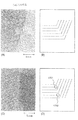
FIG. 8 shows a TEM photograph in which a crystalline silicon film having a unique crystal structure is enlarged 250,000 times. As shown in FIG. 8, the crystalline silicon film invented by the present inventors has the following characteristics.
(1) The structure of the crystal lattice is continuous continuously in a specific direction.
(2) Grows into thin rod-like (or columnar) crystals or thin flat rod-like crystals. (3) A plurality of rod-like or flat rod-like crystals are grown in parallel or substantially parallel to each other and with directivity.
[0028]
When the photograph shown in FIG. 8 is seen, for example, a thin rod-like crystal having a width of about 0.15 μm extends obliquely from the lower left to the upper right, and a clear boundary (crystal grain boundary) can be confirmed at both width edges ( The shades of lines and the like seen in the photos are due to the difference in crystal orientation). In addition, since the plurality of rod-like crystals are grown in directions substantially parallel to each other, it can be confirmed that the plurality of crystal grain boundaries also extend substantially in parallel. Since this crystal grain boundary serves as an energy barrier for carriers (electrons or holes), it is considered that carriers preferentially move only inside the rod-like crystal.
[0029]
As will be described in detail later, the crystal structure is remarkably improved in crystallinity by heat treatment at a temperature exceeding 700 ° C. containing a halogen element, and gettering is removed to such an extent that the catalyst element does not cause a problem. Yes. Therefore, it is considered that the inside of the rod-like crystal is a region in which crystal lattices are continuously connected and can be regarded as a single crystal substantially for carriers. Therefore, it is also characterized by very little impurity scattering that hinders carrier movement.
[0030]
Further, when forming the active layer of the TFT, the carrier mobility is greatly improved by designing the carrier moving direction and the crystal grain boundary extending direction to coincide with each other. This is because the movement direction of carriers is defined in one specific direction by the crystal grain boundary, so that scattering due to collision between carriers is extremely reduced. Thus, when a crystalline silicon film having a unique crystal structure is used as an active layer, it can be said that the active layer has anisotropy with respect to the behavior of carriers.
[0031]
Further, as a characteristic of the unique crystal structure, it can be mentioned that lattices are continuously joined at the grain boundary (boundary) between rod-like or flat rod-like crystals. This will be described with reference to FIG.
[0032]
FIG. 17A is an HRTEM (High Resolution TEM) photograph in which a crystal grain boundary between rod-like or flat rod-like crystals is enlarged in a crystalline silicon film having a unique crystal structure. Analysis by HRTEM is used for observation of crystal lattice images. As a result of observing lattice images at crystal grain boundaries, the present inventors have obtained the following knowledge.
[0033]
In the HRTEM photograph shown in FIG. 17A, it is confirmed that adjacent crystal regions are continuously joined with good consistency at the boundary (grain boundary) seen from the top to the bottom of the center. it can. FIG. 17B schematically shows the structure of FIG. 17A in a simplified manner. As shown in FIG. 17B, lattice images having different orientations collide with each other at the crystal grain boundary, but the atoms constituting different crystal regions at the boundary correspond to each other on a one-to-one basis. This means that lattice defects such as bonds (dangling bonds) are not formed.
[0034]
Note that the crystalline silicon film is a collection of a plurality of rod-like or flat rod-like crystals, and it is considered that the structure as shown in FIG. 17A is formed at all or substantially all of the crystal grain boundaries. . Here, “substantially all” means that even if a dangling bond of a silicon atom exists, the portion is neutralized (terminated) by hydrogen or a halogen element and thus does not become a lattice defect. .
[0035]
On the other hand, FIG. 17C shows an HRTEM photograph of a crystalline silicon film (a so-called high-temperature polysilicon film) made of another crystal structure for reference. A schematic diagram thereof is shown in FIG.
[0036]
In FIG. 17C, it can be confirmed that the lattice image of the left crystal region and the lattice image of the right crystal region are disorderly joined at the crystal grain boundary seen at the center. That is, as shown in FIG. 17D, since the atoms do not correspond one-to-one, surplus bonds exist as
[0037]
As described above, the crystalline silicon film having a unique crystal structure according to the present inventors has a completely different bonding structure from that of the conventional crystalline silicon film, and is a recombination center of carriers while being a crystal grain boundary. It has the characteristic that it must not be.
[0038]
(Characteristics of TFT using unique crystal structure)
The electrical characteristics of the TFT produced by using the crystalline silicon film having the above crystal structure as an active layer were measured with a commercially available transistor characteristic measuring instrument (manufactured by Hewlett Packard: Model No. 4145B), and the following results were obtained. .
(1) Sub-threshold coefficient, which is a parameter indicating TFT switching performance (agility of switching on / off operation), is 60-100 mV / decade for both N-type TFT and P-type TFT (typically 60-85 mV / decade) and small. This data value is almost equivalent to that of an insulated gate field effect transistor (IGFET) using single crystal silicon.
(2) Field effect mobility (μ) which is a parameter indicating the speed of operation of the TFT FE ) 200-650cm for N-type TFT 2 / Vs (typically 250-300cm 2 / Vs), 100-300cm with P-type TFT 2 / Vs (typically 150-200cm 2 / Vs). This means that the operation speed is three times higher than that of the conventional TFT.
(3) The threshold voltage (V th ) Is as low as -0.5 to 1.5 V for N-type TFTs and -1.5 to 0.5 V for P-type TFTs. This means that the power consumption can be reduced by driving with a small power supply voltage.
[0039]
As described above, the TFT composed of the crystal structure has extremely excellent switching characteristics and high-speed operation characteristics. In addition, there is a feature that it is hardly affected by the short channel effect due to a unique crystal structure. This will be described below.
[0040]
Conventionally, in the IC world, the device size has been reduced according to the scaling rule, and the degree of circuit integration and the characteristics of device elements have been improved. However, in the submicron region where the channel length (distance in the direction in which the carrier in the channel formation region moves) is 1 μm or less, the short channel effect becomes apparent, and there is a limit to the improvement of device characteristics by the scaling law. Details on the short channel effect are detailed in “Physics of VLSI Devices; Mitsumasa Koyanagi et al .; Maruzen; 1986”.
[0041]
For example, when the short channel effect occurs, the drain breakdown voltage is lowered and the device is significantly deteriorated. For this reason, the short channel effect has been suppressed by contrivances such as the channel doping method, but the impurities uniformly added to the channel formation region have hindered the movement of carriers and reduced the operation speed of the transistor. .
[0042]
However, a TFT composed of a unique crystal structure has a very high operating speed and a high drain breakdown voltage at the same time even when the channel length is as short as 0.6 μm, and is a highly reliable TFT as evaluated by an accelerated test. It has been confirmed.
[0043]
The present inventors presume that the crystal grain boundary functions effectively as the reason why the drain breakdown voltage of a TFT composed of a unique crystal structure is high. In other words, the energy barrier due to the grain boundary extending almost in parallel with the channel length direction (defined as the direction in which carriers move from the source to the drain) in the channel formation region effectively spreads the depletion layer from the drain region. It was speculated that the decrease in drain breakdown voltage due to punch-through was effectively suppressed.
[0044]
That is, in the case where the influence of the short channel effect becomes obvious with a TFT using a conventional silicon thin film, that is, even when the channel length is extremely small (0.01 to 2 μm), it is a unique crystal structure. Since the spread of the depletion layer can be suppressed, it is considered that the short channel effect can be effectively suppressed.
[0045]
Further, as described above, the short channel effect can be suppressed without adding an artificial device (such as a channel doping technique), so that an intrinsic or substantially intrinsic semiconductor film can be used as a channel formation region. This is one of the most important factors for increasing the operation speed of the TFT.
[0046]
In addition, being intrinsic or substantially intrinsic means that at least one of the following conditions is satisfied.
(1) The activation energy of the silicon film is approximately 1/2 (the Fermi level is located at the approximate center of the forbidden body).
(2) This is a region where the impurity concentration is lower than the spin density.
{Circle around (3)} An undoped or intrinsic region where impurities are not intentionally added.
[0047]
Further, as described above, since the spread of the depletion layer on the drain side is suppressed by the crystal grain boundary, the depletion layer capacitance of the TFT is greatly reduced. Here, the aforementioned subthreshold coefficient (S value) is expressed by the following approximate expression.
ln10 · kT / q [1+ (Cd + Cit) / Cox]
However, k is a Boltzmann constant, T is an absolute temperature, q is a charge amount, Cd is a depletion layer capacitance, Cit is an interface state equivalent capacitance, and Cox is a gate oxide film capacitance.
[0048]
The fact that a TFT composed of a peculiar crystal structure has a very small subthreshold coefficient as described above, and the fact that the interface state is very small (the reason will be explained in Examples) is depletion. This is considered to support the above assumption that the layer capacitance Cd is small.
[0049]
The above is nothing but an inference that combines the electrical characteristics of a crystalline silicon film having a unique crystal structure actually obtained by the present inventors and a TFT actually fabricated using the crystalline silicon film. However, the experimental data is true, and it is also true that it has excellent performance that is totally different from TFTs using conventional silicon thin films.
[0050]
(Characteristics of the circuit composed of the above TFT)
Furthermore, the frequency characteristics of a ring oscillator produced by using the TFT composed of the above unique crystal structure by the present inventors are shown. The ring oscillator is a circuit in which inverter circuits having a CMOS structure are connected in an odd-numbered ring shape, and is used to obtain a delay time per inverter circuit. The structure of the ring oscillator used in the experiment is as follows.
Number of stages: 9 stages
TFT gate insulating film thickness: 30nm and 50nm
TFT gate length: 0.6μm
[0051]
FIG. 9 shows the result of measuring the oscillation frequency of the ring oscillator when the power supply voltage is 5 V with a spectroanalyzer. In FIG. 9, the horizontal axis represents the power supply voltage (V DD ), The vertical axis represents the oscillation frequency (f osc ). As shown in FIG. 9, when a 30 nm TFT with a gate insulating film is used, an oscillation frequency of 1 GHz or more is realized.
[0052]
FIG. 10 shows the state of the output spectrum of the spectroanalyzer when an oscillation frequency of 1.04 GHz is obtained. The horizontal axis is the frequency from 1 to 1.1 GHz, and the vertical axis is the voltage (output amplitude) taken on the log scale. As apparent from FIG. 10, a peak of the output spectrum appears at 1.04 GHz. The output spectrum has a tail due to the resolution of the apparatus, and does not affect the experimental results.
[0053]
In addition, a shift register, which is actually one of the TEGs of the LSI circuit, was manufactured, and output pulses when driven at an operating frequency of 10 to 100 MHz were confirmed, and the operation performance of the shift register was examined. The screen of the oscilloscope shown in FIG. 11 (the upper side shows the clock pulse and the lower side shows the output pulse) is a shift register having a gate insulating film thickness of 30 nm, a gate length of 0.6 μm, an operating frequency of 100 MHz, a power supply voltage of 5 V, and 50 stages. It represents the output pulse of the circuit.
[0054]
As a result of confirmation by the present inventors, as shown in FIG. 12, the reciprocal number (vertical axis) of the output pulse width t and the operating frequency (horizontal axis) are in a proportional relationship, and high frequency driving of 100 MHz is possible independently. In addition, it has been found that the output pulse is a very high-performance shift register that can be obtained in an ideal state with almost no output pulse. In the experiment, two types of shift registers having slightly different circuit configurations were used, so that they were designated as
[0055]
The phenomenal data of ring oscillators and shift registers as described above show that TFTs composed of unique crystal structures have performance comparable to or better than IGFETs using single crystal silicon. ing.
[0056]
There is the following data as evidence to support it. The data shown in FIG. 13 shows the power supply voltage (V DD ), The vertical axis represents the delay time per stage of the inverter with F / O = 1 (fanout ratio is 1) (τ pd (Innovation of logic LSI technology, Kenji Maeguchi et al., P108, Science Forum, Inc., 1995). Various curves (shown by dotted lines) in the figure are data when FETs using single crystal silicon are produced with various design rules, and show so-called scaling laws.
[0057]
When the relationship between the delay time of the inverter obtained by using the above-described ring oscillator and the power supply voltage is applied to this figure, a curve indicated by a solid line in FIG. 13 is obtained. It should be noted that the channel length is 0.5 μm and the gate insulating film thickness (t OX ) Is superior in performance to an inverter manufactured with a TFT having a channel length of 0.6 μm and a gate insulating film thickness of 30 nm, compared to an inverter manufactured with an IGFET of 11 nm.
[0058]
This clearly shows that the TFT composed of the unique crystal structure invented by the present inventors has a performance superior to that of the IGFET. For example, even if the thickness of the gate insulating film constituting the TFT is set to be three times or more that of the IGFET, the gate insulating film having the same or higher performance can be obtained. That is, a TFT composed of a unique crystal structure has a higher withstand voltage than a general IGFET.
[0059]
At the same time, higher performance can be realized if a TFT composed of a unique crystal structure is miniaturized according to the scaling rule. This is possible because it is not easily affected by the short channel effect due to the unique crystal structure as described above. For example, if the ring oscillator shown in FIG. (Because the operating frequency f is inversely proportional to the square of the channel length L).
[0060]
In addition, the curve shown by the solid line (inverter using the configuration of the first invention) has a gentler slope (slope) on the lower voltage side than the curve shown by the other dotted line (inverter using a normal IGFET). It can be said that it has a particular advantage in the characteristics on the low voltage side.
[0061]
As described above, the TFT composed of the unique crystal structure invented by the present inventors has extremely excellent characteristics, and the circuit configured using the TFT realizes a high-speed operation of 10 GHz or more. It is a completely new device element. By obtaining the TFT as described above, it was possible to realize a system display equipped with a logic circuit for the first time.
[0062]
[Second Configuration of the Invention]
The present inventors have further devised to improve the degree of integration of the system display and reduce variations in TFT characteristics. Here, the configuration of the invention will be described below.
[0063]
(About addition method of catalyst element)
The crystalline silicon film having the unique crystal structure described above is formed by adding a metal element that promotes crystallization to the amorphous silicon film. The present inventors have disclosed a technique described in JP-A-8-78329 as means for transforming an amorphous silicon film into a crystalline silicon film. The technology described in the publication discloses a catalyst element (nickel, cobalt, etc.) that promotes crystallization is selectively added to the amorphous silicon film, and crystallizes in a direction substantially parallel to the substrate surface starting from the catalyst element. Only the laterally crystallized region (hereinafter referred to as a lateral growth region) is used as the active layer of the TFT.
[0064]
Note that the above-described structure of the unique crystal structure (structure consisting of an aggregate of rod-like or flat rod-like crystals) is due to such a crystallized form of the lateral growth region. Accordingly, it can be said that the lateral growth region is an aggregate of rod-like or flat rod-like crystals or an aggregate of a plurality of crystal regions arranged in a stripe shape.
[0065]
However, when the system display shown in FIG. 1 is realized, if the technique described in the publication is used as it is, restrictions on circuit design due to the addition region of the catalyst element will become apparent. For example, in the same publication, since the solution is spin-coated, the width of the addition region needs to be at least 20 μm or more. Since the addition region cannot be used as an active layer because the catalyst element is present at a high concentration, the space in the addition region becomes a dead space in circuit design as it is.
[0066]
In addition, (1) the width of the added region is limited, and (2) the same concentration of catalyst element is added to the added region, so that the lateral growth regions formed on the same substrate all have the same growth distance. In the thermal crystallization condition of 600 ° C., a lateral growth region of about 50 to 150 μm is formed. That is, in a region having a fine circuit configuration, a plurality of TFTs are formed in one lateral growth region.
[0067]
This is a major obstacle to realizing the system display shown in FIG. Basically, it is desirable that TFTs that need to be driven at high frequency and TFTs that handle analog signals have uniform characteristics as much as possible. However, even in the same lateral growth region, the crystallinity may be slightly different depending on the position. Therefore, if a plurality of TFTs are manufactured in one lateral growth region, the TFT characteristics will differ depending on the position. is there.
[0068]
In view of the above, the present inventors have proposed that the method of adding a catalytic element is an ion plantation method (ion implantation method) as a means to solve this problem that has become apparent in realizing the system display of the present invention. is doing. Here, a method of adding a catalyst element using an ion implantation method and its advantages will be described with reference to FIG.
[0069]
In FIG. 2, 201 is a substrate (including a glass substrate or a quartz substrate), 202 is a base film made of a silicon oxide film, 203 is an amorphous silicon film, and 204 is a silicon oxide film that becomes a buffer layer.
[0070]
Since these exposure methods enable formation of extremely fine patterns, a catalytic element addition region can be formed with a slit width of 0.01 to 1.0 μm (typically 0.1 to 0.35 μm). Further, if the resist pattern is directly drawn with an electron beam or the like, the degree of freedom of the shape of the added region is greatly expanded.
[0071]
Then, as shown in the left diagram of FIG. 2, ions are added so that the peak value of the
[0072]
The ion addition method may be a plasma doping method (ion doping or the like) in which mass separation is not performed in addition to the ion implantation method in which mass separation is performed, but the ion implantation method is more preferable in that only a catalyst element can be added. It is advantageous.
[0073]
Further, in the configuration shown in FIG. 2, the
[0074]
Further, since only the vicinity of the peak value of the
[0075]
This means that the lateral growth region can be formed at a desired position and with a desired width. That is, a laterally grown region having a necessary and sufficient width can be formed in consideration of the TFT size (the length of the channel formation region).
[0076]
(Outline of the second configuration)
According to the above-mentioned means, as shown in FIG. 3A, it is possible to form lateral growth regions having different growth distances on the same substrate. In FIG. 3A, 301 is a simplified diagram of a system display as shown in FIG. 1, 302 is a pixel matrix circuit, 303 and 304 are driver circuits, and 305 is a logic circuit.
[0077]
Since TFTs (pixel TFTs) constituting the pixel matrix circuit 302 are required to have a high breakdown voltage characteristic, measures such as increasing the channel length (gate length) (typically 2 to 20 μm) are taken. Therefore, as indicated by 306, the growth distance X of the lateral growth region 1 Is designed to be longer than the length of the
[0078]
On the other hand, since TFTs (logic TFTs) constituting the
[0079]
As described above, in the case of FIG. 1 , X 2 A laterally grown region having a exists on the same substrate. In this case, X 1 > X 2 It is. Growth distance X 1 , X 2 The lateral growth regions having different catalytic element concentrations n 1 , N 2 This is a region grown from the added region. In this case, n 1 > N 2 There is a relationship. That is, this configuration utilizes the phenomenon that the growth distance of the lateral growth region becomes longer as the concentration of the catalyst element present in the addition region is higher.
[0080]
In this way, even in the addition region having the same shape, a lateral growth region having a desired width can be formed by adjusting the concentration of the catalyst element added thereto. That is, when the channel length is changed according to the characteristics required by the circuit, the point of forming a lateral growth region having a different growth distance in accordance with the channel length is the main point of the second configuration of the present invention.
[0081]
Since the growth distance varies according to the channel length, there is some correlation between the channel length and the growth distance of the lateral growth region. For example, the concentration of the catalytic element is adjusted so that the distance obtained by adding a fixed margin of several μm to the channel length (or channel width) becomes the growth distance so that the channel formation region completely enters the lateral growth region, It is also possible to adjust the distance so as to be twice the length (or channel width) as the growth distance. Although this correlation can vary depending on the growth distance error and the patterning accuracy during the formation of the active layer, it cannot be said unconditionally, but is important in determining the additive concentration of the catalyst element.
[0082]
The advantage of the second configuration of the invention is that it is not necessary to enlarge the lateral growth region more than necessary particularly in the region where a fine TFT is manufactured.
[0083]
For example, when the active layer of the logic TFT shown in 309 is configured, if the width of the lateral growth region is increased more than necessary, the lateral growth region is extended to other circuits having different functions. As a result, this causes variations in TFT characteristics. When variations in TFT characteristics are caused in this way, a circuit that is driven at a very high frequency or a circuit that includes a structure that requires extremely uniform TFT characteristics, such as a differential amplifier or an operational amplifier, is configured. Cause harmful effects.
[0084]
Here, an example in which the second configuration of the present invention is applied to an operational amplifier as an example of a logic circuit will be described with reference to FIG. FIG. 4A shows an example of an operational amplifier circuit configured using eight TFTs Tr1 to Tr8, which is represented by a circuit diagram as shown in FIG.
[0085]
In FIG. 4A, 401 is an active layer composed of the above-mentioned unique crystal structure, and constitutes Tr1 to Tr8.
[0086]
At this time, the operational amplifier shown in FIG. 4A (or FIG. 4B) is configured based on a differential amplifier circuit composed of Tr4 and Tr8 (or Tr6 and Tr7). The differential amplifier circuit is characterized in that it does not affect the output because it acts on two TFTs simultaneously even if there is a temperature change or a power supply voltage change. However, this requires that the characteristics of the two TFTs are the same.
[0087]
Therefore, for example, such an arrangement that the
[0088]
Since the logic circuit composed of TFTs requires high frequency operation, the gate length is reduced to about 0.25 to 0.7 μm. Therefore, the circuit size of the operational amplifier shown in FIG. 4A is about 5 to 20 μm.
[0089]
However, in the technique described in Japanese Patent Laid-Open No. 8-78329, since the addition region of the catalyst element has a width of at least 20 μm, it is impossible to form the addition region in the gap between the TFTs. Further, since the lateral growth region becomes larger than necessary, it is impossible to devise such a technique as to align the TFT characteristics as described above. That is, the configuration shown in FIG. 4A can be achieved by using the second configuration of the present invention.
[0090]
In a fine circuit as shown in FIG. 4A, if the lateral growth region becomes too large, it interferes with the surrounding lateral growth region, which is not preferable. In the second configuration of the present invention, the growth distance of the lateral growth region can be easily controlled by adjusting the concentration of the catalytic element. Therefore, even when the addition region is formed with a fine arrangement, the lateral growth region Mutual interference can be minimized.
[0091]
Of course, when the gate length is long like the pixel TFT constituting the pixel matrix circuit, the amount of addition of the catalyst element can be increased to increase the growth distance of the lateral growth region. In addition, in the case of a fine circuit that does not cause variations in TFT characteristics, it is possible to increase the concentration of the catalytic element to form a wide lateral growth region and to form a plurality of active layers at once. .
[0092]
[Example 2]
In the system display as shown in FIG. 1 of the first embodiment, the
[0093]
Further, since the
[0094]
In this embodiment, when TFTs having different device sizes are arranged on the same substrate according to the characteristics required by the circuit, lateral growth regions having different growth distances are formed corresponding to the respective device sizes, and the regions are formed. An example is shown in which a TFT composed of a unique crystal structure is used. Here, as an example, a manufacturing process example in the case of manufacturing a CMOS circuit and a pixel TFT on the same substrate will be described with reference to FIGS.
[0095]
In FIG. 5A,
[0096]
[0097]
Next, a resist
[0098]
Then, nickel (Ni) is added by an ion implantation method as a catalyst element for promoting crystallization of the amorphous silicon film. In addition to nickel, the catalytic element is cobalt (Co), iron (Fe), tin (Sn), lead (Pb), palladium (Pd), platinum (Pt), copper (Cu), gold (Au). Etc. can be used.
[0099]
At this time, the added
[0100]
Next, after removing the resist
[0101]
As described above, the catalyst element is added at a concentration different from that of the other addition regions at least at one place on the same substrate.
[0102]
Next, when the catalyst element addition step is completed, a heat treatment is performed for 4 to 8 hours at a temperature of 500 to 700 ° C., typically 550 to 650 ° C. in an inert atmosphere or an atmosphere containing hydrogen, and then amorphous. The
[0103]
Crystallization of the
[0104]
In the present invention, only the
[0105]
When the heat treatment for crystallization is completed, patterning is performed to form island-like semiconductor layers (active layers) 510 to 512 including only a lateral growth region. Here, 510 is an active layer of an N-channel TFT constituting a CMOS circuit, 511 is an active layer of a P-channel TFT constituting a CMOS circuit, and 512 is an active layer of an N-channel TFT constituting a pixel TFT. (Fig. 5 (D))
[0106]
Even in the state shown in FIG. 5D, some traces of the presence of the
[0107]
After the formation of the
[0108]
This is because the CMOS circuit becomes a TFT with a short gate length for high-frequency driving, so that the operating voltage needs to be lowered in consideration of the low drain breakdown voltage. Therefore, it is preferable to reduce the operating voltage by reducing the threshold voltage by setting the thickness of the gate insulating film to 2 nm or more and less than 80 nm (typically 50 nm). In addition, since the pixel TFT has a high operating voltage, it is effective to devise a technique for increasing the drain breakdown voltage by setting the thickness of the gate insulating film to 80 nm to 250 nm (typically 120 nm).
[0109]
In order to form gate insulating films with different thicknesses on the same substrate, they are selectively stacked using a mask, or a thermal oxide film is formed on a specific active layer using a selective oxidation method such as the LOCOS method, A method such as increasing the film thickness may be used. Further, when the finally required gate insulating film thickness is 50 nm or less, only the thermal oxide film obtained in the subsequent thermal oxidation process can be used as the gate insulating film.
[0110]
Next, as shown in FIG. 5E, heat treatment for removing the catalytic element (nickel) by gettering (a catalytic element gettering process) is performed. This heat treatment utilizes the gettering effect of the metal element by the halogen element.
[0111]
In order to sufficiently obtain the gettering effect by the halogen element, it is preferable to perform the above heat treatment at a temperature exceeding 700 ° C. Therefore, in this embodiment, this heat treatment is performed at a temperature exceeding 700 ° C., preferably 800 to 1000 ° C. (typically 950 ° C.), and the treatment time is 0.1 to 6 hours, typically 0.5 to 1 hour. And
[0112]
Here, oxygen (O 2 ) An example in which heat treatment is performed at 950 ° C. for 30 minutes in an atmosphere containing hydrogen chloride (HCl) at a concentration of 0.5 to 10% by volume (3% by volume in this embodiment) with respect to the atmosphere. If the HCl concentration is equal to or higher than the above concentration, the surface of the active layer 209 is not preferable because the surface is uneven as much as the film thickness.
[0113]
In addition, high concentration of nitrogen (N 2 ), The oxidation rate of the crystalline silicon film can be reduced. This is an effective means for increasing the gettering time without causing the thermal oxidation reaction to proceed more than necessary.
[0114]
In addition, an example in which HCl gas is used as a compound containing a halogen element has been shown, but as other gases, typically HF, NF Three , HBr, Cl 2 , ClF Three , BCl Three , F 2 , Br 2 One or more compounds selected from halogen-containing compounds such as the above can be used.
[0115]
In this step, it is considered that nickel added to the
[0116]
The concentration of nickel in the
[0117]
In addition, a thermal oxidation reaction proceeds at the interface between the
[0118]
Furthermore, after the heat treatment in the halogen atmosphere, the heat treatment is performed at 950 ° C. for about 1 hour in a nitrogen atmosphere, thereby improving the film quality of the
[0119]
The crystalline silicon film formed through the above steps has a unique crystal structure as described in the first embodiment. That is, it is possible to realize a TFT having extremely excellent electrical characteristics as shown in the first embodiment.
[0120]
Next, an aluminum film (not shown) containing 0.2 wt% scandium is formed to form an electrode pattern to be a prototype of a later gate electrode. Then,
[0121]
At this time, the line widths (gate lengths) of the
What is necessary is just to set it as 2-20 micrometers.
[0122]
Next, the
[0123]
Next, after a resist
[0124]
n - After the
[0125]
N - Region 526-529, p - After the
[0126]
Next, a resist
[0127]
Through this process, the
[0128]
Next, the resist
[0129]
All active layers are completed as described above. When all the impurity ions are added in this manner, the resist
[0130]
Next, a titanium (Ti)
[0131]
When silicidation is completed, the
[0132]
Next, a silicon oxide film is formed as a first
[0133]
When the state shown in FIG. 7C is obtained, a second
[0134]
Then, a
[0135]
After the
It is formed to a thickness of 120 nm. (Fig. 7 (D))
[0136]
Note that a transparent conductive film (eg, an ITO film) may be used as the
[0137]
At this time, an auxiliary capacitor is formed in a region where the
[0138]
Finally, the entire substrate is heated in a hydrogen atmosphere, and the entire device is hydrogenated to compensate for dangling bonds (unbonded hands) in the film (particularly in the active layer). Through the above steps, a CMOS circuit and a pixel TFT can be manufactured on the same substrate.
[0139]
[Example 3]
In the present embodiment, an example relating to the configuration of the pixel area constituting the pixel matrix circuit in the system display as shown in FIG. 1 will be described. First, FIG. 14A shows a top view of a pixel region.
[0140]
In FIG. 14A, 1401 and 1402 are active layers, 1403 and 1404 are gate lines, and 1405 and 1406 are source lines. In practice, a plurality of source lines and gate wirings are arranged so as to be orthogonal to each other, and a plurality of matrix-arranged regions surrounded by the source lines and gate lines function as the
[0141]
In addition,
[0142]
In addition, the
[0143]
Next, 1407 is a contact portion between the active layer 1402 (source region) and the
[0144]
A region indicated by
[0145]
In addition, a pixel electrode 1411 is disposed over the
[0146]
Next, FIG. 14B shows a cross-sectional view taken along line AA ′ of FIG. Since the basic transistor structure has been described in detail in
[0147]
14B,
[0148]
Next, a source wiring 1420 (corresponding to 1405 in FIG. 14A) and a drain wiring 1421 (corresponding to 1409 in FIG. 14A) are arranged over the first interlayer insulating film 1419.
[0149]
Then, a second
[0150]
At this time, the third
[0151]
When the
[0152]
Next, 1428 is a fourth interlayer insulating film made of an organic resin film, and a
[0153]
A
[0154]
[Example 4]
In this embodiment, an example in which a CMOS circuit having a configuration different from that of
[0155]
First, FIG. 15A shows a CMOS circuit composed of silicon gate TFTs using silicon thin films (polysilicon films) imparted with one conductivity as
[0156]
With such a silicon gate structure,
[0157]
FIG. 15B shows an example in which the
[0158]
The main role of the
[0159]
The main role of the island-
[0160]
In this embodiment, contact holes are formed by a dry etching method, and the selectivity between the interlayer insulating
[0161]
As described above, by simplifying the process of forming the
[0162]
[Example 5]
It has already been described that the silicon thin film described in the first configuration of the invention is necessary to implement the present invention. In this example, an example in which a silicon thin film crystallized by means different from that in Example 2 is used in the present invention will be described.
[0163]
In FIG. 5, after obtaining the state shown in FIG. 5C (the stage where the heat treatment for crystallization is completed), the
[0164]
By the laser annealing, the amorphous component slightly remaining in the crystalline silicon thin film is crystallized and the crystallinity of the crystalline silicon is remarkably improved. The system display of the present invention can also be formed using the silicon thin film thus obtained. The advantage of this embodiment is that the system display can be formed on an inexpensive glass substrate. That is, the manufacturing cost can be reduced.
[0165]
However, the most desirable mode for carrying out the present invention is to use the TFT utilizing the silicon thin film shown in Example 1, and this example requires the use of a low heat resistant substrate such as a glass substrate as the substrate. It is preferable to use only when this occurs.
[0166]
Further, the process shown in the first embodiment and the process of the present embodiment may be combined. In other words, the catalyst element gettering process may be performed after the laser annealing step. In that case, a higher crystalline silicon thin film can be formed.
[0167]
[Example 6]
In the present invention, not only the ion implantation method described with reference to FIG. 2 but also a catalyst element can be directly added to the amorphous silicon film without using a resist mask as another embodiment.
[0168]
As a means for that, there is a technique that can irradiate ions only to a fine spot, such as a FIB (Focussed Ion Beam) method. According to such a technique, a pattern is drawn directly by a focused ion beam containing a catalytic element, and an addition region of the catalytic element can be formed in a desired shape at a desired position.
[0169]
According to this embodiment, the process of forming the resist mask and the patterning process can be simplified, so that the manufacturing cost can be reduced and the manufacturing yield can be improved.
[0170]
[Example 7]
In this example, several examples of combinations of interlayer insulating films (first to third) shown in Example 2 will be described.
[0171]
First, in FIG. 7D, as a first
[0172]
Under the experimental conditions of the present inventors, the film formation temperature (about 300 ° C.) of the
[0173]
With such a configuration, the following advantages can be obtained.
(1) Since acrylic is photosensitive and can be directly patterned without using a resist mask, the manufacturing process can be simplified.
(2) Since acrylic is less expensive than polyimide, manufacturing costs can be reduced.
(3) The adhesion between ITO and acrylic is better than the adhesion between ITO and polyimide.
(4) Since acrylic is superior in flatness, the electric field applied on the pixel electrode can be made uniform.
[0174]
As another example, all interlayer insulating films can be formed of polyimide, or all interlayer insulating films can be formed of acrylic. However, in the case where all the interlayer insulating films are formed of acrylic, it is a condition that all the steps after the acrylic is formed are performed at a temperature lower than the heat resistant temperature of acrylic.
[0175]
[Example 8]
The present invention can be applied to any semiconductor device, and any semiconductor device in which a circuit is configured using a TFT on a substrate having an insulating surface falls within the applicable range. Such a semiconductor device may function only as a logic circuit like an IC or VLSI, or may function as a display display like an active matrix electro-optical device.
[0176]
In particular, as an active matrix type electro-optical device, an active matrix type liquid crystal display device, an active matrix type EL display device, an active matrix type EC display device, and the like using a system display with a built-in logic circuit as shown in FIG. Can be applied.
[0177]
Such active matrix display devices are roughly classified into a transmissive display device and a reflective display device. For example, in a transmissive liquid crystal display device, a backlight is disposed on the back side of an active matrix substrate (substrate on which TFTs are arranged), and an image is recognized by viewing light transmitted through the display device. The reflective liquid crystal display device recognizes an image by reflecting light incident from the surface side of the active matrix substrate by a pixel electrode disposed on the active matrix substrate and viewing the reflected light.
[0178]
Although there is no significant difference in TFT structure between the transmission type display device and the reflection type display device, it is characterized in that the material forming the pixel electrode is different. For example, in the case of manufacturing a transmissive display device, a transparent electrode such as ITO may be used as the pixel electrode 1411 in FIG. In the case of a reflective display device, an opaque electrode with high reflection efficiency may be used as the pixel electrode 1411.
[0179]
As described above, the present invention can be applied to both a transmissive display device and a reflective display device if the TFT structure is slightly changed. In particular, since the reflective display device does not have a problem with the aperture ratio, it has an advantage that the degree of freedom of design is widened compared to the transmissive display device. For example, in the transmissive liquid crystal display device, the pixel region is almost composed of a window portion that transmits light like the
[0180]
[Example 9]
In this embodiment, an application product using an electro-optical device as shown in
[0181]
Examples of semiconductor devices using the present invention include (digital) video cameras, (digital) still cameras, head mounted displays, car navigation systems, personal computers, personal digital assistants (mobile computers, mobile phones, etc.) and the like.
[0182]
FIG. 16A illustrates a mobile computer that includes a main body 2001, a camera unit 2002, an
[0183]
FIG. 16B illustrates a head-mounted display, which includes a
[0184]
FIG. 16C illustrates a car navigation system, which includes a
[0185]
FIG. 16D illustrates a cellular phone, which includes a
[0186]
FIG. 16E illustrates a video camera which includes a main body 2401, a display device 2402, an
[0187]
As described above, the application range of the present invention is extremely wide and can be applied to display media in various fields. In addition, by applying the present invention, the active matrix display device itself can have various functions, so that the size of the electro-optical device becomes extremely small. In the future, it can be a portable electro-optical device carded by a system display.
[0188]
【The invention's effect】
First, the structure of the first invention, which is extremely important for carrying out the present invention, is that a crystalline silicon film crystallized by using a catalytic element is subjected to a catalytic element gettering process by a halogen element. A silicon thin film having a unique crystal structure is obtained.
[0189]
A TFT using a silicon thin film formed by a manufacturing process as shown in Example 2 has a subthreshold coefficient comparable to a MOSFET using single crystal silicon, and has a high field effect mobility. There is. In addition, a silicon thin film having a crystal structure made up of a plurality of rod-like or flat rod-like crystals has an effect of suppressing the short channel effect itself, and there is no need to rely on the channel doping method or the like even if the TFT is miniaturized. High breakdown voltage and high speed operation characteristics can be realized.
[0190]
By using TFTs having such extremely high performance, that is, a wide driving frequency range and operating voltage range, it is possible to form a high frequency driving type TFT and a high breakdown voltage driving type TFT on the same substrate.
[0191]
According to a second aspect of the invention, a lateral growth region having a desired growth distance can be formed at a desired position by using an ion implantation method as a method for adding a catalyst element. With this technology, even when a circuit is composed of extremely fine TFTs with a channel length (gate length) of 0.25 to 0.7 μm, a lateral growth region of an appropriate size can be formed according to the circuit arrangement, so that the device characteristics Can be aligned.
[0192]
With the above effects, a semiconductor device in which a logic circuit is formed using a TFT over a substrate having an insulating surface can be manufactured. Further, a logic circuit built-in type semiconductor device in which a logic circuit, a driver circuit, and a pixel matrix circuit in which a high-frequency driving TFT and a high breakdown voltage driving TFT are mixedly mounted on the same substrate can be realized.
[0193]
Since the semiconductor device of the present invention is equipped with a logic circuit that can include a display control circuit, a memory circuit, and ultimately an arithmetic circuit in addition to the pixel matrix circuit and the driver circuit, the system is extremely multifunctional and highly portable. Functions as a display. In addition, since the high-frequency drive circuit is designed so that the operating voltage does not increase more than necessary, it is excellent in low power consumption.
[0194]
Further, by applying such a semiconductor device to, for example, a liquid crystal display device or an application product using the same as a display monitor, it is possible to provide an extremely small, lightweight, and inexpensive product.
[Brief description of the drawings]
FIG. 1 is a top view of a system display.
FIG. 2 is a view for explaining an ion implantation step.
FIG. 3 is a diagram for explaining a second configuration of the invention.
FIG. 4 is a diagram showing a structure and a circuit configuration of an operational amplifier circuit.
FIGS. 5A and 5B are diagrams illustrating a manufacturing process of a CMOS circuit and a pixel TFT. FIGS.
6A and 6B are diagrams illustrating a manufacturing process of a CMOS circuit and a pixel TFT.
FIGS. 7A and 7B are diagrams illustrating a manufacturing process of a CMOS circuit and a pixel TFT. FIGS.
FIG. 8 is a photograph for explaining a unique crystal structure.
FIG. 9 is a diagram showing frequency characteristics of a ring oscillator.
FIG. 10 is a photograph showing an output spectrum of a ring oscillator.
FIG. 11 is a photograph showing an output pulse of a shift register.
FIG. 12 is a diagram showing the relationship between frequency and pulse width.
FIG. 13 is a diagram for explaining a scaling law.
FIG. 14 is a diagram for explaining a configuration and a structure of a pixel region.
FIG. 15 shows a structure of a CMOS circuit.
FIG. 16 is a diagram for illustrating an application product.
FIG. 17 is a photograph for explaining a lattice state of a crystal grain boundary.
[Explanation of symbols]
101 substrate
102 Pixel matrix circuit
103 Source line driver circuit
104 Gate line driver circuit
105 logic circuit
106, 107 Source line
108, 109 Gate line
110 pixel area
111 pixel TFT
112 Liquid crystal cell
113 Auxiliary capacity
114 phase comparator
115 LPF
116 Voltage controlled oscillator
117 frequency divider
118 Horizontal Scan Oscillator
119 Vertical scanning oscillator
120 D / A converter
121 Analog signal input terminal
122-bit signal input terminal
123 Input terminal for horizontal scanning synchronization signal
124 Input terminal for synchronization signal for vertical scanning
Claims (7)
前記非晶質シリコン膜に対して選択的に複数の領域に非晶質シリコン膜の結晶化を助長する触媒元素を添加し、
加熱処理により前記触媒元素が添加された複数の領域を起点として前記非晶質シリコン膜を結晶化させ、結晶シリコン膜でなる横成長領域を複数形成し、
前記触媒元素はイオン注入法またはプラズマドーピング法により、前記複数の領域のうち少なくとも1ヶ所の領域には他の領域とは異なる濃度で添加されることを特徴とする半導体装置の作製方法。Forming an amorphous silicon film over a substrate having an insulating surface;
A catalytic element for promoting crystallization of the amorphous silicon film is selectively added to the plurality of regions with respect to the amorphous silicon film;
The amorphous silicon film a plurality of realm which the catalyst element has been added by the heat treatment as a starting point to crystallize, the lateral growth region form a plurality made in crystalline silicon film,
The catalyst element by an ion implantation method or a plasma doping method, a method for manufacturing a semiconductor device in realm of at least one place, characterized in that it is added at different concentrations of the other realm of the plurality of regions.
前記非晶質シリコン膜に対して選択的に複数の領域に非晶質シリコン膜の結晶化を助長する触媒元素を添加し、
加熱処理により前記触媒元素が添加された複数の領域を起点として前記非晶質シリコン膜を結晶化させ、結晶シリコン膜でなる横成長領域を複数形成し、
複数の前記横成長領域の端部及び複数の前記触媒元素が添加された領域を除去するようにパターニングを行い、チャネル形成領域が前記横成長領域から構成される活性層を複数形成し、
前記触媒元素はイオン注入法またはプラズマドーピング法により、前記複数の領域のうち少なくとも1ヶ所の領域には他の領域とは異なる濃度で添加されることを特徴とする半導体装置の作製方法。Forming an amorphous silicon film over a substrate having an insulating surface;
A catalytic element for promoting crystallization of the amorphous silicon film is selectively added to the plurality of regions with respect to the amorphous silicon film;
The amorphous silicon film a plurality of realm which the catalyst element has been added by the heat treatment as a starting point to crystallize, the lateral growth region form a plurality made in crystalline silicon film,
In patterning is performed so as to remove a plurality of realm that end and more of the catalyst element is added in the lateral growth region, the channel formation region is forming a plurality constituted active layer from the lateral growth region,
The catalyst element by an ion implantation method or a plasma doping method, a method for manufacturing a semiconductor device in realm of at least one place, characterized in that it is added at different concentrations of the other realm of the plurality of regions.
前記触媒元素が添加される領域の短辺の長さは0.01〜1μmであることを特徴とする半導体装置の作製方法。 In claim 1 or claim 2 ,
A method for manufacturing a semiconductor device, wherein a length of a short side of the region to which the catalyst element is added is 0.01 to 1 μm.
前記触媒元素としてNi、Fe、Co、Sn、Pd、Pb、Pt、Cu、Auから選ばれた一種の元素を用いることを特徴とする半導体装置の作製方法。 In any one of Claims 1 to 3 ,
A method for manufacturing a semiconductor device, wherein one of elements selected from Ni, Fe, Co, Sn, Pd, Pb, Pt, Cu, and Au is used as the catalyst element.
前記複数形成された横成長領域のうち、第1の濃度で前記触媒元素が添加された領域を起点とする前記横成長領域からは、画素マトリクス回路を構成するTFTの活性層が形成され、第2の濃度で前記触媒元素が添加された領域を起点とする前記横成長領域からは、ロジック回路またはドライバー回路を構成するTFTの活性層が形成され、前記第1の濃度は前記第2の濃度よりも高濃度であることを特徴とする半導体装置の作製方法。 In any one of Claims 1 thru | or 4 ,
Wherein among the plurality formed lateral growth region, from the lateral growth region of the realm of the catalyst element is added at a first concentration to the starting point, the active layer of the TFT constituting the pixel matrix circuit is formed, from the lateral growth region originating from the realm of the catalyst element is added at a second concentration, the active layer of the TFT constituting the logic circuit or driver circuit is formed, the first concentration is the second A method for manufacturing a semiconductor device, characterized in that the concentration is higher than the concentration of.
前記結晶シリコン膜をハロゲン元素を含む雰囲気中で加熱処理することで、前記結晶シリコン膜中の前記触媒元素を除去することを特徴とする半導体装置の作製方法。 In any one of Claims 1 thru | or 5 ,
A method for manufacturing a semiconductor device, wherein the catalytic element in the crystalline silicon film is removed by heat-treating the crystalline silicon film in an atmosphere containing a halogen element.
前記ハロゲン元素を含む雰囲気中にはHCl、HF、NF3、HBr、Cl2、ClF3、BCl3、F2、Br2から選ばれた一種または複数種が存在していることを特徴とする半導体装置の作製方法。 In claim 6 ,
One or more kinds selected from HCl, HF, NF 3 , HBr, Cl 2 , ClF 3 , BCl 3 , F 2 and Br 2 are present in the atmosphere containing the halogen element. A method for manufacturing a semiconductor device.
Priority Applications (13)
| Application Number | Priority Date | Filing Date | Title |
|---|---|---|---|
| JP2207797A JP3753827B2 (en) | 1997-01-20 | 1997-01-20 | Method for manufacturing semiconductor device |
| TW087100259A TW386238B (en) | 1997-01-20 | 1998-01-09 | Semiconductor device and method of manufacturing the same |
| US09/006,844 US6380560B1 (en) | 1997-01-20 | 1998-01-14 | Semiconductor device forming a pixel matrix circuit |
| CNB98105837XA CN1173412C (en) | 1997-01-20 | 1998-01-20 | Semiconductor device and mfg. method thereof |
| KR10-1998-0001529A KR100465416B1 (en) | 1997-01-20 | 1998-01-20 | Semiconductor device and method of manufacturing the same |
| CNB2004100642546A CN100377363C (en) | 1997-01-20 | 1998-01-20 | A portable information terminal and a camera |
| CNB2006101007978A CN100470739C (en) | 1997-01-20 | 1998-01-20 | Portal information terminal and vedio camera |
| CNB2006101014083A CN100505309C (en) | 1997-01-20 | 1998-01-20 | A portable information terminal and a camera |
| CN200610101412XA CN1877861B (en) | 1997-01-20 | 1998-01-20 | Semiconductor device and use thereof |
| US10/107,113 US6730932B2 (en) | 1997-01-20 | 2002-03-26 | Semiconductor device and method of manufacturing the same |
| US10/753,524 US20040164300A1 (en) | 1997-01-20 | 2004-01-09 | Semiconductor device and method of manufacturing the same |
| US13/462,032 US8723182B2 (en) | 1997-01-20 | 2012-05-02 | Semiconductor device and method of manufacturing the same |
| US14/274,888 US9389477B2 (en) | 1997-01-20 | 2014-05-12 | Semiconductor device and method of manufacturing the same |
Applications Claiming Priority (1)
| Application Number | Priority Date | Filing Date | Title |
|---|---|---|---|
| JP2207797A JP3753827B2 (en) | 1997-01-20 | 1997-01-20 | Method for manufacturing semiconductor device |
Publications (2)
| Publication Number | Publication Date |
|---|---|
| JPH10209465A JPH10209465A (en) | 1998-08-07 |
| JP3753827B2 true JP3753827B2 (en) | 2006-03-08 |
Family
ID=12072834
Family Applications (1)
| Application Number | Title | Priority Date | Filing Date |
|---|---|---|---|
| JP2207797A Expired - Fee Related JP3753827B2 (en) | 1997-01-20 | 1997-01-20 | Method for manufacturing semiconductor device |
Country Status (2)
| Country | Link |
|---|---|
| JP (1) | JP3753827B2 (en) |
| CN (3) | CN1877861B (en) |
Families Citing this family (12)
| Publication number | Priority date | Publication date | Assignee | Title |
|---|---|---|---|---|
| TW386238B (en) | 1997-01-20 | 2000-04-01 | Semiconductor Energy Lab | Semiconductor device and method of manufacturing the same |
| JP3846057B2 (en) * | 1998-09-03 | 2006-11-15 | セイコーエプソン株式会社 | Electro-optical device drive circuit, electro-optical device, and electronic apparatus |
| JP4476390B2 (en) | 1998-09-04 | 2010-06-09 | 株式会社半導体エネルギー研究所 | Method for manufacturing semiconductor device |
| EP2309482A3 (en) | 1998-10-30 | 2013-04-24 | Semiconductor Energy Laboratory Co, Ltd. | Field sequantial liquid crystal display device and driving method thereof, and head mounted display |
| US6506635B1 (en) | 1999-02-12 | 2003-01-14 | Semiconductor Energy Laboratory Co., Ltd. | Semiconductor device, and method of forming the same |
| JP4731655B2 (en) * | 1999-02-12 | 2011-07-27 | 株式会社半導体エネルギー研究所 | Method for manufacturing semiconductor device |
| US6680487B1 (en) * | 1999-05-14 | 2004-01-20 | Semiconductor Energy Laboratory Co., Ltd. | Semiconductor comprising a TFT provided on a substrate having an insulating surface and method of fabricating the same |
| JP4627843B2 (en) * | 1999-07-22 | 2011-02-09 | 株式会社半導体エネルギー研究所 | Semiconductor device |
| JP4823543B2 (en) * | 2004-03-26 | 2011-11-24 | 株式会社半導体エネルギー研究所 | Method for manufacturing semiconductor device |
| KR102268217B1 (en) | 2010-03-05 | 2021-06-24 | 가부시키가이샤 한도오따이 에네루기 켄큐쇼 | Display device |
| CN105576037B (en) * | 2016-01-08 | 2018-11-13 | 京东方科技集团股份有限公司 | Thin film transistor (TFT) and its making and test method, array substrate and display device |
| US20190229173A1 (en) * | 2018-01-23 | 2019-07-25 | Int Tech Co., Ltd. | Light emitting device and manufacturing method thereof |
Family Cites Families (3)
| Publication number | Priority date | Publication date | Assignee | Title |
|---|---|---|---|---|
| US4728617A (en) * | 1986-11-04 | 1988-03-01 | Intel Corporation | Method of fabricating a MOSFET with graded source and drain regions |
| US5572211A (en) * | 1994-01-18 | 1996-11-05 | Vivid Semiconductor, Inc. | Integrated circuit for driving liquid crystal display using multi-level D/A converter |
| US5539219A (en) * | 1995-05-19 | 1996-07-23 | Ois Optical Imaging Systems, Inc. | Thin film transistor with reduced channel length for liquid crystal displays |
-
1997
- 1997-01-20 JP JP2207797A patent/JP3753827B2/en not_active Expired - Fee Related
-
1998
- 1998-01-20 CN CN200610101412XA patent/CN1877861B/en not_active Expired - Fee Related
- 1998-01-20 CN CNB2006101007978A patent/CN100470739C/en not_active Expired - Fee Related
- 1998-01-20 CN CNB2006101014083A patent/CN100505309C/en not_active Expired - Fee Related
Also Published As
| Publication number | Publication date |
|---|---|
| CN100505309C (en) | 2009-06-24 |
| CN100470739C (en) | 2009-03-18 |
| JPH10209465A (en) | 1998-08-07 |
| CN1877861B (en) | 2010-05-12 |
| CN1921149A (en) | 2007-02-28 |
| CN1877861A (en) | 2006-12-13 |
| CN1897233A (en) | 2007-01-17 |
Similar Documents
| Publication | Publication Date | Title |
|---|---|---|
| US6730932B2 (en) | Semiconductor device and method of manufacturing the same | |
| JP4401448B2 (en) | Method for manufacturing semiconductor device | |
| JP4086925B2 (en) | Active matrix display | |
| JP4068219B2 (en) | Method for manufacturing semiconductor device | |
| JP4115283B2 (en) | Semiconductor device and manufacturing method thereof | |
| JP4566294B2 (en) | Continuous grain boundary crystalline silicon film, semiconductor device | |
| US20030138996A1 (en) | Semiconductor device and method of fabricating the same | |
| JP2000036598A (en) | Semiconductor device provided with semiconductor circuit consisting of semiconductor element, and manufacture thereof | |
| US6452211B1 (en) | Semiconductor thin film and semiconductor device | |
| JP3753827B2 (en) | Method for manufacturing semiconductor device | |
| JPH1140815A (en) | Semiconductor device and manufacture thereof | |
| JP4397439B2 (en) | Semiconductor device | |
| JPH11103068A (en) | Semiconductor device and manufacture thereof | |
| JPH11261076A (en) | Semiconductor device and its manufacture | |
| JPH11354443A (en) | Semiconductor thin film and semiconductor device | |
| JPH10223530A (en) | Manufacturing method for semiconductor device | |
| JPH10301147A (en) | Semiconductor device and its manufacture | |
| KR100955380B1 (en) | Fabrication method of polycrystalline liquid crystal display device | |
| KR100560047B1 (en) | Semiconductor thin film and semiconductor device | |
| JPH10214975A (en) | Semiconductor device and fabrication thereof | |
| JP2000058838A (en) | Semiconductor device provided with semiconductor circuit composed of semiconductor element and its manufacture | |
| JPH11307781A (en) | Thin film transistor and its manufacture |
Legal Events
| Date | Code | Title | Description |
|---|---|---|---|
| A521 | Written amendment |
Free format text: JAPANESE INTERMEDIATE CODE: A523 Effective date: 20040116 |
|
| A621 | Written request for application examination |
Free format text: JAPANESE INTERMEDIATE CODE: A621 Effective date: 20040116 |
|
| A521 | Written amendment |
Free format text: JAPANESE INTERMEDIATE CODE: A523 Effective date: 20040409 |
|
| A521 | Written amendment |
Free format text: JAPANESE INTERMEDIATE CODE: A523 Effective date: 20040409 |
|
| A977 | Report on retrieval |
Free format text: JAPANESE INTERMEDIATE CODE: A971007 Effective date: 20050623 |
|
| A131 | Notification of reasons for refusal |
Free format text: JAPANESE INTERMEDIATE CODE: A131 Effective date: 20050913 |
|
| A521 | Written amendment |
Free format text: JAPANESE INTERMEDIATE CODE: A523 Effective date: 20051020 |
|
| TRDD | Decision of grant or rejection written | ||
| A01 | Written decision to grant a patent or to grant a registration (utility model) |
Free format text: JAPANESE INTERMEDIATE CODE: A01 Effective date: 20051213 |
|
| A61 | First payment of annual fees (during grant procedure) |
Free format text: JAPANESE INTERMEDIATE CODE: A61 Effective date: 20051214 |
|
| R150 | Certificate of patent or registration of utility model |
Free format text: JAPANESE INTERMEDIATE CODE: R150 |
|
| FPAY | Renewal fee payment (event date is renewal date of database) |
Free format text: PAYMENT UNTIL: 20091222 Year of fee payment: 4 |
|
| FPAY | Renewal fee payment (event date is renewal date of database) |
Free format text: PAYMENT UNTIL: 20091222 Year of fee payment: 4 |
|
| FPAY | Renewal fee payment (event date is renewal date of database) |
Free format text: PAYMENT UNTIL: 20091222 Year of fee payment: 4 |
|
| FPAY | Renewal fee payment (event date is renewal date of database) |
Free format text: PAYMENT UNTIL: 20101222 Year of fee payment: 5 |
|
| FPAY | Renewal fee payment (event date is renewal date of database) |
Free format text: PAYMENT UNTIL: 20101222 Year of fee payment: 5 |
|
| FPAY | Renewal fee payment (event date is renewal date of database) |
Free format text: PAYMENT UNTIL: 20111222 Year of fee payment: 6 |
|
| FPAY | Renewal fee payment (event date is renewal date of database) |
Free format text: PAYMENT UNTIL: 20111222 Year of fee payment: 6 |
|
| FPAY | Renewal fee payment (event date is renewal date of database) |
Free format text: PAYMENT UNTIL: 20121222 Year of fee payment: 7 |
|
| FPAY | Renewal fee payment (event date is renewal date of database) |
Free format text: PAYMENT UNTIL: 20121222 Year of fee payment: 7 |
|
| FPAY | Renewal fee payment (event date is renewal date of database) |
Free format text: PAYMENT UNTIL: 20131222 Year of fee payment: 8 |
|
| R250 | Receipt of annual fees |
Free format text: JAPANESE INTERMEDIATE CODE: R250 |
|
| R250 | Receipt of annual fees |
Free format text: JAPANESE INTERMEDIATE CODE: R250 |
|
| LAPS | Cancellation because of no payment of annual fees |