JP6177588B2 - Method for manufacturing metal oxide semiconductor substrate and method for manufacturing light-emitting device - Google Patents
Method for manufacturing metal oxide semiconductor substrate and method for manufacturing light-emitting device Download PDFInfo
- Publication number
- JP6177588B2 JP6177588B2 JP2013113252A JP2013113252A JP6177588B2 JP 6177588 B2 JP6177588 B2 JP 6177588B2 JP 2013113252 A JP2013113252 A JP 2013113252A JP 2013113252 A JP2013113252 A JP 2013113252A JP 6177588 B2 JP6177588 B2 JP 6177588B2
- Authority
- JP
- Japan
- Prior art keywords
- caac
- substrate
- oxide semiconductor
- metal oxide
- semiconductor substrate
- Prior art date
- Legal status (The legal status is an assumption and is not a legal conclusion. Google has not performed a legal analysis and makes no representation as to the accuracy of the status listed.)
- Expired - Fee Related
Links
- 239000000758 substrate Substances 0.000 title claims description 110
- 239000004065 semiconductor Substances 0.000 title claims description 49
- 238000000034 method Methods 0.000 title claims description 34
- 229910044991 metal oxide Inorganic materials 0.000 title claims description 27
- 150000004706 metal oxides Chemical class 0.000 title claims description 27
- 238000004519 manufacturing process Methods 0.000 title claims description 24
- 239000013078 crystal Substances 0.000 claims description 57
- 150000001875 compounds Chemical class 0.000 claims description 46
- 239000000843 powder Substances 0.000 claims description 46
- 229910052733 gallium Inorganic materials 0.000 claims description 18
- 239000011701 zinc Substances 0.000 claims description 18
- 229910052738 indium Inorganic materials 0.000 claims description 17
- GYHNNYVSQQEPJS-UHFFFAOYSA-N Gallium Chemical compound [Ga] GYHNNYVSQQEPJS-UHFFFAOYSA-N 0.000 claims description 14
- APFVFJFRJDLVQX-UHFFFAOYSA-N indium atom Chemical compound [In] APFVFJFRJDLVQX-UHFFFAOYSA-N 0.000 claims description 13
- 229910052725 zinc Inorganic materials 0.000 claims description 10
- 239000002994 raw material Substances 0.000 claims description 8
- HCHKCACWOHOZIP-UHFFFAOYSA-N Zinc Chemical compound [Zn] HCHKCACWOHOZIP-UHFFFAOYSA-N 0.000 claims description 6
- 238000010304 firing Methods 0.000 claims description 5
- 238000003892 spreading Methods 0.000 claims description 4
- 239000010410 layer Substances 0.000 description 78
- 238000010438 heat treatment Methods 0.000 description 18
- 229910002601 GaN Inorganic materials 0.000 description 17
- JMASRVWKEDWRBT-UHFFFAOYSA-N Gallium nitride Chemical compound [Ga]#N JMASRVWKEDWRBT-UHFFFAOYSA-N 0.000 description 16
- XLOMVQKBTHCTTD-UHFFFAOYSA-N Zinc monoxide Chemical compound [Zn]=O XLOMVQKBTHCTTD-UHFFFAOYSA-N 0.000 description 16
- 238000005253 cladding Methods 0.000 description 15
- IJGRMHOSHXDMSA-UHFFFAOYSA-N Atomic nitrogen Chemical compound N#N IJGRMHOSHXDMSA-UHFFFAOYSA-N 0.000 description 13
- 239000012298 atmosphere Substances 0.000 description 12
- 230000015572 biosynthetic process Effects 0.000 description 8
- 229910052751 metal Inorganic materials 0.000 description 8
- 239000011787 zinc oxide Substances 0.000 description 8
- 239000002184 metal Substances 0.000 description 7
- 229910052757 nitrogen Inorganic materials 0.000 description 7
- QGZKDVFQNNGYKY-UHFFFAOYSA-N Ammonia Chemical compound N QGZKDVFQNNGYKY-UHFFFAOYSA-N 0.000 description 6
- 229910007541 Zn O Inorganic materials 0.000 description 6
- 239000012299 nitrogen atmosphere Substances 0.000 description 6
- QVGXLLKOCUKJST-UHFFFAOYSA-N atomic oxygen Chemical compound [O] QVGXLLKOCUKJST-UHFFFAOYSA-N 0.000 description 4
- AJNVQOSZGJRYEI-UHFFFAOYSA-N digallium;oxygen(2-) Chemical compound [O-2].[O-2].[O-2].[Ga+3].[Ga+3] AJNVQOSZGJRYEI-UHFFFAOYSA-N 0.000 description 4
- 229910001195 gallium oxide Inorganic materials 0.000 description 4
- 239000007789 gas Substances 0.000 description 4
- 229910003437 indium oxide Inorganic materials 0.000 description 4
- PJXISJQVUVHSOJ-UHFFFAOYSA-N indium(iii) oxide Chemical compound [O-2].[O-2].[O-2].[In+3].[In+3] PJXISJQVUVHSOJ-UHFFFAOYSA-N 0.000 description 4
- 239000001301 oxygen Substances 0.000 description 4
- 229910052760 oxygen Inorganic materials 0.000 description 4
- 229910001233 yttria-stabilized zirconia Inorganic materials 0.000 description 4
- 229910052782 aluminium Inorganic materials 0.000 description 3
- 229910021529 ammonia Inorganic materials 0.000 description 3
- 239000011261 inert gas Substances 0.000 description 3
- 239000000463 material Substances 0.000 description 3
- 239000000203 mixture Substances 0.000 description 3
- 238000001451 molecular beam epitaxy Methods 0.000 description 3
- 229910052594 sapphire Inorganic materials 0.000 description 3
- 239000010980 sapphire Substances 0.000 description 3
- 238000001947 vapour-phase growth Methods 0.000 description 3
- XKRFYHLGVUSROY-UHFFFAOYSA-N Argon Chemical compound [Ar] XKRFYHLGVUSROY-UHFFFAOYSA-N 0.000 description 2
- OKTJSMMVPCPJKN-UHFFFAOYSA-N Carbon Chemical compound [C] OKTJSMMVPCPJKN-UHFFFAOYSA-N 0.000 description 2
- FYYHWMGAXLPEAU-UHFFFAOYSA-N Magnesium Chemical compound [Mg] FYYHWMGAXLPEAU-UHFFFAOYSA-N 0.000 description 2
- PXHVJJICTQNCMI-UHFFFAOYSA-N Nickel Chemical compound [Ni] PXHVJJICTQNCMI-UHFFFAOYSA-N 0.000 description 2
- VYPSYNLAJGMNEJ-UHFFFAOYSA-N Silicium dioxide Chemical compound O=[Si]=O VYPSYNLAJGMNEJ-UHFFFAOYSA-N 0.000 description 2
- GWEVSGVZZGPLCZ-UHFFFAOYSA-N Titan oxide Chemical compound O=[Ti]=O GWEVSGVZZGPLCZ-UHFFFAOYSA-N 0.000 description 2
- 238000002441 X-ray diffraction Methods 0.000 description 2
- XAGFODPZIPBFFR-UHFFFAOYSA-N aluminium Chemical compound [Al] XAGFODPZIPBFFR-UHFFFAOYSA-N 0.000 description 2
- 238000004458 analytical method Methods 0.000 description 2
- 125000004429 atom Chemical group 0.000 description 2
- 238000000231 atomic layer deposition Methods 0.000 description 2
- 229910052795 boron group element Inorganic materials 0.000 description 2
- 238000006243 chemical reaction Methods 0.000 description 2
- 238000005229 chemical vapour deposition Methods 0.000 description 2
- 239000004020 conductor Substances 0.000 description 2
- 238000002425 crystallisation Methods 0.000 description 2
- 230000008025 crystallization Effects 0.000 description 2
- 230000002349 favourable effect Effects 0.000 description 2
- 229910052735 hafnium Inorganic materials 0.000 description 2
- AMGQUBHHOARCQH-UHFFFAOYSA-N indium;oxotin Chemical compound [In].[Sn]=O AMGQUBHHOARCQH-UHFFFAOYSA-N 0.000 description 2
- 239000011777 magnesium Substances 0.000 description 2
- 229910052749 magnesium Inorganic materials 0.000 description 2
- 238000000465 moulding Methods 0.000 description 2
- 150000004767 nitrides Chemical class 0.000 description 2
- QGLKJKCYBOYXKC-UHFFFAOYSA-N nonaoxidotritungsten Chemical compound O=[W]1(=O)O[W](=O)(=O)O[W](=O)(=O)O1 QGLKJKCYBOYXKC-UHFFFAOYSA-N 0.000 description 2
- BASFCYQUMIYNBI-UHFFFAOYSA-N platinum Chemical compound [Pt] BASFCYQUMIYNBI-UHFFFAOYSA-N 0.000 description 2
- 229910052696 pnictogen Inorganic materials 0.000 description 2
- 230000005855 radiation Effects 0.000 description 2
- 238000004151 rapid thermal annealing Methods 0.000 description 2
- 230000002040 relaxant effect Effects 0.000 description 2
- 239000002356 single layer Substances 0.000 description 2
- 238000004544 sputter deposition Methods 0.000 description 2
- 229910052719 titanium Inorganic materials 0.000 description 2
- 239000010936 titanium Substances 0.000 description 2
- OGIDPMRJRNCKJF-UHFFFAOYSA-N titanium oxide Inorganic materials [Ti]=O OGIDPMRJRNCKJF-UHFFFAOYSA-N 0.000 description 2
- 229910001930 tungsten oxide Inorganic materials 0.000 description 2
- 229910052726 zirconium Inorganic materials 0.000 description 2
- ZOXJGFHDIHLPTG-UHFFFAOYSA-N Boron Chemical compound [B] ZOXJGFHDIHLPTG-UHFFFAOYSA-N 0.000 description 1
- 229910052684 Cerium Inorganic materials 0.000 description 1
- VYZAMTAEIAYCRO-UHFFFAOYSA-N Chromium Chemical compound [Cr] VYZAMTAEIAYCRO-UHFFFAOYSA-N 0.000 description 1
- RYGMFSIKBFXOCR-UHFFFAOYSA-N Copper Chemical compound [Cu] RYGMFSIKBFXOCR-UHFFFAOYSA-N 0.000 description 1
- DGAQECJNVWCQMB-PUAWFVPOSA-M Ilexoside XXIX Chemical compound C[C@@H]1CC[C@@]2(CC[C@@]3(C(=CC[C@H]4[C@]3(CC[C@@H]5[C@@]4(CC[C@@H](C5(C)C)OS(=O)(=O)[O-])C)C)[C@@H]2[C@]1(C)O)C)C(=O)O[C@H]6[C@@H]([C@H]([C@@H]([C@H](O6)CO)O)O)O.[Na+] DGAQECJNVWCQMB-PUAWFVPOSA-M 0.000 description 1
- ZOKXTWBITQBERF-UHFFFAOYSA-N Molybdenum Chemical compound [Mo] ZOKXTWBITQBERF-UHFFFAOYSA-N 0.000 description 1
- 229910052779 Neodymium Inorganic materials 0.000 description 1
- OAICVXFJPJFONN-UHFFFAOYSA-N Phosphorus Chemical compound [P] OAICVXFJPJFONN-UHFFFAOYSA-N 0.000 description 1
- ATJFFYVFTNAWJD-UHFFFAOYSA-N Tin Chemical compound [Sn] ATJFFYVFTNAWJD-UHFFFAOYSA-N 0.000 description 1
- RTAQQCXQSZGOHL-UHFFFAOYSA-N Titanium Chemical compound [Ti] RTAQQCXQSZGOHL-UHFFFAOYSA-N 0.000 description 1
- QCWXUUIWCKQGHC-UHFFFAOYSA-N Zirconium Chemical compound [Zr] QCWXUUIWCKQGHC-UHFFFAOYSA-N 0.000 description 1
- 229910045601 alloy Inorganic materials 0.000 description 1
- 239000000956 alloy Substances 0.000 description 1
- RNQKDQAVIXDKAG-UHFFFAOYSA-N aluminum gallium Chemical compound [Al].[Ga] RNQKDQAVIXDKAG-UHFFFAOYSA-N 0.000 description 1
- 229910052787 antimony Inorganic materials 0.000 description 1
- WATWJIUSRGPENY-UHFFFAOYSA-N antimony atom Chemical compound [Sb] WATWJIUSRGPENY-UHFFFAOYSA-N 0.000 description 1
- 229910052786 argon Inorganic materials 0.000 description 1
- 229910052785 arsenic Inorganic materials 0.000 description 1
- RQNWIZPPADIBDY-UHFFFAOYSA-N arsenic atom Chemical compound [As] RQNWIZPPADIBDY-UHFFFAOYSA-N 0.000 description 1
- NWAIGJYBQQYSPW-UHFFFAOYSA-N azanylidyneindigane Chemical compound [In]#N NWAIGJYBQQYSPW-UHFFFAOYSA-N 0.000 description 1
- 230000005540 biological transmission Effects 0.000 description 1
- 229910052797 bismuth Inorganic materials 0.000 description 1
- JCXGWMGPZLAOME-UHFFFAOYSA-N bismuth atom Chemical compound [Bi] JCXGWMGPZLAOME-UHFFFAOYSA-N 0.000 description 1
- 229910052796 boron Inorganic materials 0.000 description 1
- 238000001354 calcination Methods 0.000 description 1
- 229910052799 carbon Inorganic materials 0.000 description 1
- 229910052804 chromium Inorganic materials 0.000 description 1
- 239000011651 chromium Substances 0.000 description 1
- 229910017052 cobalt Inorganic materials 0.000 description 1
- 239000010941 cobalt Substances 0.000 description 1
- GUTLYIVDDKVIGB-UHFFFAOYSA-N cobalt atom Chemical compound [Co] GUTLYIVDDKVIGB-UHFFFAOYSA-N 0.000 description 1
- 229910052802 copper Inorganic materials 0.000 description 1
- 239000010949 copper Substances 0.000 description 1
- PMHQVHHXPFUNSP-UHFFFAOYSA-M copper(1+);methylsulfanylmethane;bromide Chemical compound Br[Cu].CSC PMHQVHHXPFUNSP-UHFFFAOYSA-M 0.000 description 1
- 238000000151 deposition Methods 0.000 description 1
- 238000011161 development Methods 0.000 description 1
- 238000009826 distribution Methods 0.000 description 1
- 229910021389 graphene Inorganic materials 0.000 description 1
- VBJZVLUMGGDVMO-UHFFFAOYSA-N hafnium atom Chemical compound [Hf] VBJZVLUMGGDVMO-UHFFFAOYSA-N 0.000 description 1
- 229910052736 halogen Inorganic materials 0.000 description 1
- 150000002367 halogens Chemical class 0.000 description 1
- 150000004678 hydrides Chemical class 0.000 description 1
- 239000012535 impurity Substances 0.000 description 1
- 229910052746 lanthanum Inorganic materials 0.000 description 1
- QSHDDOUJBYECFT-UHFFFAOYSA-N mercury Chemical compound [Hg] QSHDDOUJBYECFT-UHFFFAOYSA-N 0.000 description 1
- 229910052753 mercury Inorganic materials 0.000 description 1
- 229910001507 metal halide Inorganic materials 0.000 description 1
- 150000005309 metal halides Chemical class 0.000 description 1
- 150000002739 metals Chemical class 0.000 description 1
- 229910052750 molybdenum Inorganic materials 0.000 description 1
- 239000011733 molybdenum Substances 0.000 description 1
- 229910052759 nickel Inorganic materials 0.000 description 1
- 229910052758 niobium Inorganic materials 0.000 description 1
- 239000010955 niobium Substances 0.000 description 1
- GUCVJGMIXFAOAE-UHFFFAOYSA-N niobium atom Chemical compound [Nb] GUCVJGMIXFAOAE-UHFFFAOYSA-N 0.000 description 1
- QJGQUHMNIGDVPM-UHFFFAOYSA-N nitrogen group Chemical group [N] QJGQUHMNIGDVPM-UHFFFAOYSA-N 0.000 description 1
- -1 organic indium Chemical compound 0.000 description 1
- 230000003647 oxidation Effects 0.000 description 1
- 238000007254 oxidation reaction Methods 0.000 description 1
- 230000001590 oxidative effect Effects 0.000 description 1
- 125000004430 oxygen atom Chemical group O* 0.000 description 1
- 229910052698 phosphorus Inorganic materials 0.000 description 1
- 239000011574 phosphorus Substances 0.000 description 1
- 229910052697 platinum Inorganic materials 0.000 description 1
- 238000005498 polishing Methods 0.000 description 1
- 238000010298 pulverizing process Methods 0.000 description 1
- 238000012827 research and development Methods 0.000 description 1
- 229910052814 silicon oxide Inorganic materials 0.000 description 1
- 229910052709 silver Inorganic materials 0.000 description 1
- 239000004332 silver Substances 0.000 description 1
- 239000011734 sodium Substances 0.000 description 1
- 229910052708 sodium Inorganic materials 0.000 description 1
- 238000005477 sputtering target Methods 0.000 description 1
- 239000000126 substance Substances 0.000 description 1
- 229910052715 tantalum Inorganic materials 0.000 description 1
- GUVRBAGPIYLISA-UHFFFAOYSA-N tantalum atom Chemical compound [Ta] GUVRBAGPIYLISA-UHFFFAOYSA-N 0.000 description 1
- 229910052716 thallium Inorganic materials 0.000 description 1
- BKVIYDNLLOSFOA-UHFFFAOYSA-N thallium Chemical compound [Tl] BKVIYDNLLOSFOA-UHFFFAOYSA-N 0.000 description 1
- 229910052718 tin Inorganic materials 0.000 description 1
- WFKWXMTUELFFGS-UHFFFAOYSA-N tungsten Chemical compound [W] WFKWXMTUELFFGS-UHFFFAOYSA-N 0.000 description 1
- 229910052721 tungsten Inorganic materials 0.000 description 1
- 239000010937 tungsten Substances 0.000 description 1
- 229910052720 vanadium Inorganic materials 0.000 description 1
- GPPXJZIENCGNKB-UHFFFAOYSA-N vanadium Chemical compound [V]#[V] GPPXJZIENCGNKB-UHFFFAOYSA-N 0.000 description 1
- 229910052724 xenon Inorganic materials 0.000 description 1
- FHNFHKCVQCLJFQ-UHFFFAOYSA-N xenon atom Chemical compound [Xe] FHNFHKCVQCLJFQ-UHFFFAOYSA-N 0.000 description 1
- 229910052727 yttrium Inorganic materials 0.000 description 1
- YVTHLONGBIQYBO-UHFFFAOYSA-N zinc indium(3+) oxygen(2-) Chemical compound [O--].[Zn++].[In+3] YVTHLONGBIQYBO-UHFFFAOYSA-N 0.000 description 1
Images


Classifications
-
- H—ELECTRICITY
- H01—ELECTRIC ELEMENTS
- H01L—SEMICONDUCTOR DEVICES NOT COVERED BY CLASS H10
- H01L33/00—Semiconductor devices with at least one potential-jump barrier or surface barrier specially adapted for light emission; Processes or apparatus specially adapted for the manufacture or treatment thereof or of parts thereof; Details thereof
- H01L33/02—Semiconductor devices with at least one potential-jump barrier or surface barrier specially adapted for light emission; Processes or apparatus specially adapted for the manufacture or treatment thereof or of parts thereof; Details thereof characterised by the semiconductor bodies
- H01L33/26—Materials of the light emitting region
- H01L33/30—Materials of the light emitting region containing only elements of group III and group V of the periodic system
-
- H—ELECTRICITY
- H01—ELECTRIC ELEMENTS
- H01L—SEMICONDUCTOR DEVICES NOT COVERED BY CLASS H10
- H01L33/00—Semiconductor devices with at least one potential-jump barrier or surface barrier specially adapted for light emission; Processes or apparatus specially adapted for the manufacture or treatment thereof or of parts thereof; Details thereof
- H01L33/005—Processes
- H01L33/0062—Processes for devices with an active region comprising only III-V compounds
- H01L33/0066—Processes for devices with an active region comprising only III-V compounds with a substrate not being a III-V compound
-
- H—ELECTRICITY
- H01—ELECTRIC ELEMENTS
- H01L—SEMICONDUCTOR DEVICES NOT COVERED BY CLASS H10
- H01L33/00—Semiconductor devices with at least one potential-jump barrier or surface barrier specially adapted for light emission; Processes or apparatus specially adapted for the manufacture or treatment thereof or of parts thereof; Details thereof
- H01L33/02—Semiconductor devices with at least one potential-jump barrier or surface barrier specially adapted for light emission; Processes or apparatus specially adapted for the manufacture or treatment thereof or of parts thereof; Details thereof characterised by the semiconductor bodies
- H01L33/16—Semiconductor devices with at least one potential-jump barrier or surface barrier specially adapted for light emission; Processes or apparatus specially adapted for the manufacture or treatment thereof or of parts thereof; Details thereof characterised by the semiconductor bodies with a particular crystal structure or orientation, e.g. polycrystalline, amorphous or porous
-
- H—ELECTRICITY
- H01—ELECTRIC ELEMENTS
- H01L—SEMICONDUCTOR DEVICES NOT COVERED BY CLASS H10
- H01L33/00—Semiconductor devices with at least one potential-jump barrier or surface barrier specially adapted for light emission; Processes or apparatus specially adapted for the manufacture or treatment thereof or of parts thereof; Details thereof
- H01L33/02—Semiconductor devices with at least one potential-jump barrier or surface barrier specially adapted for light emission; Processes or apparatus specially adapted for the manufacture or treatment thereof or of parts thereof; Details thereof characterised by the semiconductor bodies
- H01L33/26—Materials of the light emitting region
- H01L33/30—Materials of the light emitting region containing only elements of group III and group V of the periodic system
- H01L33/32—Materials of the light emitting region containing only elements of group III and group V of the periodic system containing nitrogen
Landscapes
- Engineering & Computer Science (AREA)
- Manufacturing & Machinery (AREA)
- Computer Hardware Design (AREA)
- Microelectronics & Electronic Packaging (AREA)
- Power Engineering (AREA)
- Thin Film Transistor (AREA)
- Led Devices (AREA)
Description
発光デバイス、及び発光デバイスの作製方法に関する。 The present invention relates to a light emitting device and a method for manufacturing the light emitting device.
窒化ガリウムを用いた発光ダイオード(LED:Light Emitting Diode)の開発が進んでおり、照明デバイス等に広く実用化が進められている。 Development of a light emitting diode (LED) using gallium nitride has been advanced, and its practical application has been promoted widely in lighting devices and the like.
発光効率や耐久寿命などの発光デバイスの特性には、発光層の結晶品質が大きく影響する。発光デバイスを構成する基板として、安価なサファイア基板などが多く使用されているが、発光層の結晶品質は発光層の形成される基板によって左右されるため、該結晶品質の良好な発光層が得られるような発光デバイス用基板として窒化ガリウム単結晶基板が研究されている(例えば、特許文献1参照)。 The crystal quality of the light-emitting layer greatly affects the characteristics of the light-emitting device such as light emission efficiency and durability life. As a substrate constituting a light emitting device, an inexpensive sapphire substrate or the like is often used. However, since the crystal quality of the light emitting layer depends on the substrate on which the light emitting layer is formed, a light emitting layer with good crystal quality is obtained. As such a light emitting device substrate, a gallium nitride single crystal substrate has been studied (for example, see Patent Document 1).
また、単結晶酸化ガリウムからなる主面を有する酸化ガリウム基板を用いた窒化ガリウム系の発光ダイオードについても研究開発が進められている(例えば、特許文献2参照)。 Research and development is also underway for gallium nitride-based light-emitting diodes using a gallium oxide substrate having a main surface made of single-crystal gallium oxide (see, for example, Patent Document 2).
発光デバイスを作製するための基板として用いられる窒化ガリウム基板や酸化ガリウム基板は、エピタキシャル成長させた結晶表面を形成するために、単結晶膜を成長させるプロセスが必要であった。 A gallium nitride substrate or a gallium oxide substrate used as a substrate for manufacturing a light-emitting device requires a process of growing a single crystal film in order to form an epitaxially grown crystal surface.
本発明はこのような状況に鑑みなされたものであり、生産性に優れた新規の発光デバイスを提供することを課題の一とする。 The present invention has been made in view of such a situation, and an object thereof is to provide a novel light-emitting device with excellent productivity.
本発明の一形態は、発光デバイスの支持基板としてc軸配向した結晶領域を含む金属酸化物半導体(CAAC−OS(C Axis Aligned Crystalline Oxide Semiconductor))基板を用いる。c軸配向した結晶領域は、c軸が金属酸化物半導体の支持基板の表面に対して略垂直に配向したものである。本明細書においては、c軸が表面に概略垂直である結晶部を含む酸化物半導体基板をCAAC−OS基板という。なお、本明細書においては、CAAC−OS基板とは、CAAC−OS膜(層)も含む。 In one embodiment of the present invention, a metal oxide semiconductor (CAAC-OS (C Axis Crystalline Oxide Semiconductor)) substrate including a c-axis aligned crystal region is used as a supporting substrate of a light-emitting device. The c-axis oriented crystal region is one in which the c-axis is oriented substantially perpendicular to the surface of the metal oxide semiconductor support substrate. In this specification, an oxide semiconductor substrate including a crystal part whose c-axis is substantially perpendicular to the surface is referred to as a CAAC-OS substrate. Note that in this specification, a CAAC-OS substrate includes a CAAC-OS film (layer).
例えば、CAAC−OSとして、ガリウムを含むCAAC−OS、インジウム及びガリウムを含むCAAC−OS、又はインジウム、ガリウム、及び亜鉛を含むCAAC−OS等を用いることができる。 For example, as the CAAC-OS, a CAAC-OS containing gallium, a CAAC-OS containing indium and gallium, a CAAC-OS containing indium, gallium, and zinc, or the like can be used.
発光デバイスにおいて基板は、CAAC−OS基板単層でもよいし、サファイア基板、又はイットリア安定化ジルコニア(YSZ)基板などの基底基板上に薄膜のCAAC−OS基板が積層された構造でもよい。 In the light-emitting device, the substrate may be a single layer of a CAAC-OS substrate, or a structure in which a thin CAAC-OS substrate is stacked over a base substrate such as a sapphire substrate or a yttria-stabilized zirconia (YSZ) substrate.
CAAC−OS基板は作製時に、700℃〜1500℃程度の高温における加熱処理を行う。該加熱処理は、窒素雰囲気下、又は窒素及びアンモニア雰囲気下で行うことができる。また、窒素雰囲気下、及び酸素雰囲気下両方において加熱処理を行ってもよい。 The CAAC-OS substrate is subjected to heat treatment at a high temperature of about 700 ° C. to 1500 ° C. at the time of manufacturing. The heat treatment can be performed in a nitrogen atmosphere or in a nitrogen and ammonia atmosphere. Further, heat treatment may be performed in both a nitrogen atmosphere and an oxygen atmosphere.
従って、CAAC−OS基板は、比較的簡便な作製工程で形成することが可能であり、かつ良好な結晶品質を有する。 Therefore, the CAAC-OS substrate can be formed through a relatively simple manufacturing process and has favorable crystal quality.
発光ダイオード(LED)層には13族−15族化合物半導体(III−V族化合物半導体)を用いることができる。LED層は、発光層を挟持する一対のクラッド層を含み、CAAC−OS基板との間にバッファ層を有することが好ましい。また、LED層は、第1の電極層及び第2の電極層によって間に挟持される。バッファ層は、CAAC−OS基板及び発光ダイオード層(クラッド層)において格子定数が異なる場合、格子不整合を緩和させる機能を有する膜である。バッファ層はLED層と同種の13族−15族化合物半導体を用いることができる。 A 13-15 group compound semiconductor (III-V compound semiconductor) can be used for a light emitting diode (LED) layer. The LED layer preferably includes a pair of clad layers that sandwich the light-emitting layer, and has a buffer layer between the LED layer and the CAAC-OS substrate. The LED layer is sandwiched between the first electrode layer and the second electrode layer. The buffer layer is a film having a function of relaxing lattice mismatch when lattice constants are different between the CAAC-OS substrate and the light-emitting diode layer (cladding layer). For the buffer layer, the same group 13-15 compound semiconductor as the LED layer can be used.
本明細書で開示する発明の構成の一形態は、金属酸化物半導体基板上に発光ダイオード層が設けられ、金属酸化物半導体基板はc軸が金属酸化物半導体基板の表面に概略垂直である結晶部を含む発光デバイスである。 One embodiment of the structure of the invention disclosed in this specification is a crystal in which a light-emitting diode layer is provided over a metal oxide semiconductor substrate, and the c-axis of the metal oxide semiconductor substrate is substantially perpendicular to the surface of the metal oxide semiconductor substrate. A light emitting device including a portion.
本明細書で開示する発明の構成の他の一形態は、上記構成において、金属酸化物半導体基板と発光ダイオード層との間にバッファ層を有する発光デバイスである。 Another embodiment of the structure of the invention disclosed in this specification is a light-emitting device having a buffer layer between a metal oxide semiconductor substrate and a light-emitting diode layer in the above structure.
本明細書で開示する発明の構成の他の一形態は、上記構成において、金属酸化物半導体基板は、基底基板上に設けられている発光デバイスである。 Another embodiment of the structure of the invention disclosed in this specification is a light-emitting device in which the metal oxide semiconductor substrate is provided over a base substrate in the above structure.
本明細書で開示する発明の構成の他の一形態は、上記構成において、発光ダイオード層は、順に積層する第1のクラッド層、発光層、及び第2のクラッド層を含み、第1のクラッド層、発光層、及び第2のクラッド層は13族−15族化合物半導体である発光デバイスである。 Another embodiment of the structure of the invention disclosed in this specification is that, in the above structure, the light-emitting diode layer includes a first clad layer, a light-emitting layer, and a second clad layer that are sequentially stacked, and the first clad The layer, the light emitting layer, and the second cladding layer are a light emitting device that is a group 13-15 compound semiconductor.
本明細書で開示する発明の構成の他の一形態は、上記構成において、発光ダイオード層は、金属酸化物半導体基板側から、順に積層する第1のクラッド層、発光層、及び第2のクラッド層を含み、第1のクラッド層は、n型13族−15族化合物半導体、発光層は13族−15族化合物半導体、第2のクラッド層はp型13族−15族化合物半導体である発光デバイスである。 Another embodiment of the structure of the invention disclosed in this specification is the above structure, in which the light-emitting diode layer includes a first clad layer, a light-emitting layer, and a second clad that are sequentially stacked from the metal oxide semiconductor substrate side. The first clad layer is an n-type group 13-15 compound semiconductor, the light emitting layer is a group 13-15 compound semiconductor, and the second clad layer is a p-type group 13-15 compound semiconductor. It is a device.
本明細書で開示する発明の構成の他の一形態は、上記発光デバイスを用いる電子機器を提供するものである。 Another embodiment of the structure of the invention disclosed in this specification provides an electronic device using the light-emitting device.
LED層が設けられるCAAC−OS基板は、比較的簡便な作製工程で形成することが可能であり、かつ良好な結晶品質を有する。 A CAAC-OS substrate provided with an LED layer can be formed by a relatively simple manufacturing process and has good crystal quality.
従って、生産性に優れた新規発光デバイスの提供することができる。 Therefore, a novel light-emitting device with excellent productivity can be provided.
実施の形態について、図面を用いて詳細に説明する。但し、以下の説明に限定されず、趣旨及びその範囲から逸脱することなくその形態及び詳細を様々に変更し得ることは当業者であれば容易に理解される。従って、以下に示す実施の形態の記載内容に限定して解釈されるものではない。なお、以下に説明する構成において、同一部分又は同様な機能を有する部分には同一の符号を異なる図面間で共通して用い、その繰り返しの説明は省略する。 Embodiments will be described in detail with reference to the drawings. However, it is not limited to the following description, and it will be easily understood by those skilled in the art that modes and details can be variously changed without departing from the spirit and scope of the invention. Therefore, the present invention is not construed as being limited to the description of the embodiments below. Note that in the structures described below, the same portions or portions having similar functions are denoted by the same reference numerals in different drawings, and description thereof is not repeated.
なお、第1、第2、又は第3として付される序数詞は便宜上用いるものであり、工程順又は積層順を示すものではない。また、本明細書において発明を特定するための事項として固有の名称を示すものではない。 In addition, the ordinal numbers attached as the first, second, or third are used for convenience, and do not indicate the process order or the stacking order. In addition, a specific name is not shown as a matter for specifying the invention in this specification.
(実施の形態1)
本発明の一に係る発光デバイスについて、図1及び図2を用いて説明する。
(Embodiment 1)
A light-emitting device according to an embodiment of the present invention will be described with reference to FIGS.
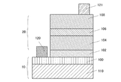
図1は、発光デバイスの基板10であるCAAC−OS基板100上に、バッファ層102を介して、第1クラッド層104、発光層106、及び第2クラッド層108が順に積層されるLED層20が設けられた発光デバイスである。
FIG. 1 shows an
また、図2は、発光デバイスの基板10である基底基板110及びCAAC−OS基板100上に、バッファ層102を介して、第1クラッド層104、発光層106、及び第2クラッド層108が順に積層されるLED層20が設けられ、基底基板110上に第1の電極層120、第2クラッド層108上に第2の電極層121が設けられた発光デバイスである。
In FIG. 2, the
基板は、図1のようにCAAC−OS基板単層でもよいし、図2のように、サファイア基板、又はイットリア安定化ジルコニア(YSZ)基板などの基底基板110上にCAAC−OS基板100が積層された構造でもよい。
The substrate may be a single layer of a CAAC-OS substrate as shown in FIG. 1, or a CAAC-
CAAC−OS基板100として、ガリウムを含むCAAC−OS、インジウム及びガリウムを含むCAAC−OS、又はインジウム、ガリウム、及び亜鉛を含むCAAC−OS等を用いることができる。
As the CAAC-
また、CAAC−OS基板100は、作製時に、700℃〜1500℃程度の高温における加熱処理を行う。該加熱処理により、インジウムや亜鉛などが基板外部へ蒸発(放出)してしまう場合があり、結果、形成されるCAAC−OS基板100は、ガリウムと比較して、インジウム、亜鉛の含有量が微量である場合がある。
In addition, the CAAC-
LED層20に含まれる層には13族−15族化合物半導体を用いることができる。
For the layer included in the
バッファ層102は、CAAC−OS基板100及びLED層20(第1クラッド層104)において格子定数が異なる場合、格子不整合を緩和させる機能を有する膜である。バッファ層102はLED層20と同種の13族−15族化合物半導体を用いることができる。
The
13族−15族化合物半導体(III−V族化合物半導体)は13族元素と15族元素を組み合わせた半導体である。13族元素としてはアルミニウム、ガリウム、インジウムなど、15族元素としては窒素、リン、ヒ素、アンチモンなどを用いることができる。また、ボロン、タリウム、ビスマスもその13族−15族化合物半導体を構成する元素として用いることができる。また、窒素を用いた窒化ガリウム、窒化アルミニウム、窒化インジウム等は窒化物半導体ともいう。 A group 13-15 group compound semiconductor (III-V compound semiconductor) is a semiconductor in which a group 13 element and a group 15 element are combined. Aluminum, gallium, indium, etc. can be used as the group 13 element, and nitrogen, phosphorus, arsenic, antimony, etc. can be used as the group 15 element. Boron, thallium, and bismuth can also be used as elements constituting the group 13-15 group compound semiconductor. In addition, gallium nitride, aluminum nitride, indium nitride, or the like using nitrogen is also referred to as a nitride semiconductor.
本実施の形態では、13族−15族化合物半導体として窒化ガリウムを用いる。バッファ層102として窒化ガリウム膜、第1クラッド層104としてn型窒化ガリウム膜、発光層106として窒化ガリウム膜、第2クラッド層としてp型窒化ガリウム膜をそれぞれ用いる。
In this embodiment, gallium nitride is used as the group 13-15 group compound semiconductor. A gallium nitride film is used as the
例えば、バッファ層102として窒化ガリウム膜、第1クラッド層104としてn型窒化ガリウム膜(シリコンを添加した窒化ガリウム膜)、発光層106とし窒化インジウムガリウム膜、第2クラッド層としてp型窒化ガリウム膜(マグネシウムを添加した窒化ガリウム膜)をそれぞれ用いることができる。また、第2クラッド層としてマグネシウムを添加した窒化アルミニウムガリウム膜を用いてもよい。
For example, a gallium nitride film as the
13族−15族化合物半導体膜は、有機金属化学的気相堆積(MOCVD)法、ハイドライド(hydride)気相成長(VPE)法や分子線エピタキシャル(MBE)法等の気相成長手段を用いて形成することができる。 The group 13-15 compound semiconductor film is formed using vapor phase growth means such as metal organic chemical vapor deposition (MOCVD) method, hydride vapor phase growth (VPE) method, molecular beam epitaxy (MBE) method or the like. Can be formed.
また、図2においては、第1の電極層120は陰極、第2の電極層121は陽極として機能する。第1の電極層120、第2の電極層121としては、酸化物導電膜や金属膜を用いることができる。例えば、インジウム錫酸化物、酸化インジウムに酸化亜鉛を混合した導電材料、酸化インジウムに酸化シリコンを混合した導電材料、有機インジウム、有機スズ、酸化タングステンを含むインジウム酸化物、酸化タングステンを含むインジウム亜鉛酸化物、酸化チタンを含むインジウム酸化物、酸化チタンを含むインジウム錫酸化物、グラフェン、又はタングステン、モリブデン、ジルコニウム、ハフニウム、バナジウム、ニオブ、タンタル、クロム、コバルト、ニッケル、チタン、白金、アルミニウム、銅、銀等の金属、又はその合金、若しくはその金属窒化物から一つ、又は複数種を用いて形成することができる。
In FIG. 2, the
CAAC−OS基板100に用いることのできるCAAC−OSは、複数の結晶部を有し、その結晶粒界が不明確である。なお、CAAC−OS中の当該結晶部は、一辺が100nm未満の立方体内に収まる大きさであることが多い。また、透過型電子顕微鏡(TEM:Transmission Electron Microscope)による観察像では、CAAC−OSに含まれる結晶部と結晶部との境界は明確ではない。また、TEMによってCAAC−OSには粒界(グレインバウンダリーともいう。)は確認できない。そのため、CAAC−OSは、粒界に起因する電子移動度の低下が抑制される。
A CAAC-OS that can be used for the CAAC-
CAAC−OSは、例えば、複数の結晶部を有し、当該複数の結晶部においてc軸が被形成面の法線ベクトルまたは表面の法線ベクトルに平行な方向に揃っている場合がある。そのため、CAAC−OSは、例えば、X線回折(XRD:X−Ray Diffraction)装置を用い、out−of−plane法による分析を行うと、2θが31°近傍のピークが現れる場合がある。2θが31°近傍のピークは、InGaZnO4の結晶であれば、(009)面に配向していることを示す。また、CAAC−OSは、例えば、2θが36°近傍のピークが現れる場合がある。2θが36°近傍のピークは、Ga2ZnO4の結晶であれば、(222)面に配向していることを示す。CAAC−OSは、好ましくは、2θが31°近傍にピークが現れ、2θが36°近傍にピークが現れない。 For example, the CAAC-OS includes a plurality of crystal parts, and the c-axis is aligned in a direction parallel to the normal vector of the surface to be formed or the normal vector of the surface of the plurality of crystal parts. Therefore, when CAAC-OS is analyzed by an out-of-plane method using, for example, an X-ray diffraction (XRD) apparatus, a peak at 2θ of around 31 ° may appear. The peak at 2θ of around 31 ° indicates that it is oriented in the (009) plane in the case of InGaZnO 4 crystal. In the CAAC-OS, for example, a peak where 2θ is around 36 ° may appear. The peak at 2θ of around 36 ° indicates that the crystal is oriented to the (222) plane if it is a Ga 2 ZnO 4 crystal. The CAAC-OS preferably has a peak at 2θ of around 31 ° and no peak at 2θ of around 36 °.
また、CAAC−OSは、例えば、異なる結晶部間で、それぞれa軸およびb軸の向きが揃っていない場合がある。例えば、InGaZnO4の結晶を有するCAAC−OSであれば、XRD装置を用い、c軸に垂直な方向からX線を入射させるin−plane法による分析を行うと、2θが56°近傍のピークが現れる場合がある。2θが56°近傍のピークは、InGaZnO4の結晶の(110)面からの回折ピークである。ここで、2θを56°近傍で固定し、表面の法線ベクトルを軸(φ軸)として試料を回転させて分析(φスキャン)を行うと、a軸およびb軸の向きが揃っている単結晶酸化物半導体の場合は6つの対称性のピークが現れるが、CAAC−OSの場合は明瞭なピークが現れない。 In the CAAC-OS, for example, the directions of the a-axis and the b-axis may not be uniform between different crystal parts. For example, in the case of a CAAC-OS including an InGaZnO 4 crystal, when an analysis is performed by an in-plane method in which X-rays are incident from a direction perpendicular to the c-axis using an XRD apparatus, a peak at 2θ of around 56 ° is obtained. May appear. The peak at 2θ of around 56 ° is a diffraction peak from the (110) plane of the InGaZnO 4 crystal. Here, when 2θ is fixed in the vicinity of 56 ° and the sample is rotated with the surface normal vector as the axis (φ axis) and the analysis (φ scan) is performed, the directions of the a axis and the b axis are aligned. In the case of a crystalline oxide semiconductor, six symmetry peaks appear, but in the case of a CAAC-OS, a clear peak does not appear.
このように、CAAC−OSは、例えば、c軸配向し、a軸または/およびb軸はマクロに揃っていない場合がある。 Thus, for example, the CAAC-OS may be c-axis oriented and the a-axis and / or b-axis may not be aligned in a macro manner.
CAAC−OS含まれる結晶部は、c軸がCAAC−OSの被形成面の法線ベクトルまたは表面の法線ベクトルに平行な方向に揃い、かつa−b面に垂直な方向から見て三角形状または六角形状の原子配列を有し、c軸に垂直な方向から見て金属原子が層状または金属原子と酸素原子とが層状に配列している。なお、異なる結晶部間で、それぞれa軸およびb軸の向きが異なっていてもよい。本明細書において、単に垂直と記載する場合、85°以上95°以下の範囲も含まれることとする。また、単に平行と記載する場合、−5°以上5°以下の範囲も含まれることとする。 The crystal part included in the CAAC-OS has a triangular shape when the c-axis is aligned in a direction parallel to the normal vector of the CAAC-OS formation surface or the normal vector of the surface and viewed from the direction perpendicular to the ab plane. Alternatively, it has a hexagonal atomic arrangement, and metal atoms are arranged in layers or metal atoms and oxygen atoms are arranged in layers as viewed from the direction perpendicular to the c-axis. Note that the directions of the a-axis and the b-axis may be different between different crystal parts. In this specification, a simple term “perpendicular” includes a range from 85 ° to 95 °. In addition, a simple term “parallel” includes a range from −5 ° to 5 °.
CAAC−OSには複数の結晶部が含まれるが、CAAC−OSに含まれる結晶部のc軸は、それぞれCAAC−OSの被形成面の法線ベクトルまたは表面の法線ベクトルに平行な方向に揃うため、CAAC−OSの形状(被形成面の断面形状または表面の断面形状)によっては、結晶部のc軸は互いに異なる方向を向くことがある。なお、結晶部のc軸の方向は、CAAC−OSが形成されたときの被形成面の法線ベクトルまたは表面の法線ベクトルに平行な方向となる。結晶部は、成膜することにより、または成膜後に熱処理などの結晶化処理を行うことにより形成される。 The CAAC-OS includes a plurality of crystal parts. The c-axis of the crystal part included in the CAAC-OS is in a direction parallel to the normal vector of the surface to be formed of the CAAC-OS or the normal vector of the surface, respectively. Therefore, depending on the shape of the CAAC-OS (the cross-sectional shape of the surface to be formed or the cross-sectional shape of the surface), the c-axis of the crystal part may face different directions. Note that the c-axis direction of the crystal part is parallel to the normal vector of the surface where the CAAC-OS is formed or the normal vector of the surface. The crystal part is formed by film formation or by performing crystallization treatment such as heat treatment after film formation.
なお、CAAC−OSにおいて、結晶部の分布が一様でなくてもよい。例えば、CAAC−OSの形成過程において、酸化物半導体膜の表面側から結晶成長させる場合、被形成面の近傍に対し表面の近傍では結晶部の占める割合が高くなることがある。 Note that in the CAAC-OS, the distribution of crystal parts may not be uniform. For example, in the formation process of the CAAC-OS, in the case where crystal growth is performed from the surface side of the oxide semiconductor film, the ratio of crystal parts in the vicinity of the surface is higher in the vicinity of the formation surface.
CAAC−OSに用いる酸化物半導体としては、酸化ガリウム、In−Ga系酸化物、In−Ga−Zn系酸化物(IGZOとも表記する)などを用いることができる。 As an oxide semiconductor used for the CAAC-OS, gallium oxide, an In—Ga-based oxide, an In—Ga—Zn-based oxide (also referred to as IGZO), or the like can be used.
なお、ここで、例えば、In−Ga−Zn系酸化物とは、InとGaとZnを主成分として有する酸化物という意味であり、InとGaとZnの比率は問わない。また、InとGaとZn以外の金属元素が入っていてもよい。 Note that here, for example, an In—Ga—Zn-based oxide means an oxide containing In, Ga, and Zn as its main components, and there is no limitation on the ratio of In, Ga, and Zn. Moreover, metal elements other than In, Ga, and Zn may be contained.
例えば、In:Ga:Zn=1:1:1(=1/3:1/3:1/3)、In:Ga:Zn=2:2:1(=2/5:2/5:1/5)、あるいはIn:Ga:Zn=3:1:2(=1/2:1/6:1/3)の原子数比のIn−Ga−Zn系酸化物やその組成の近傍の酸化物を用いることができる。 For example, In: Ga: Zn = 1: 1: 1 (= 1/3: 1/3: 1/3), In: Ga: Zn = 2: 2: 1 (= 2/5: 2/5: 1) / 5), or an In—Ga—Zn-based oxide having an atomic ratio of In: Ga: Zn = 3: 1: 2 (= 1/2: 1/6: 1/3) and oxidation in the vicinity of the composition. Can be used.
なお、例えば、In、Ga、Znの原子数比がIn:Ga:Zn=a:b:c(a+b+c=1)である酸化物の組成が、原子数比がIn:Ga:Zn=A:B:C(A+B+C=1)の酸化物の組成の近傍であるとは、a、b、cが、(a−A)2+(b−B)2+(c−C)2≦r2を満たすことをいい、rは、例えば、0.05とすればよい。他の酸化物でも同様である。 Note that for example, the composition of an oxide in which the atomic ratio of In, Ga, and Zn is In: Ga: Zn = a: b: c (a + b + c = 1) has an atomic ratio of In: Ga: Zn = A: B: C (A + B + C = 1) is in the vicinity of the oxide composition, a, b, c are (a−A) 2 + (b−B) 2 + (c−C) 2 ≦ r 2 R may be 0.05, for example. The same applies to other oxides.
なお、酸化物半導体を構成する酸素の一部は窒素で置換されてもよい。 Note that part of oxygen included in the oxide semiconductor may be replaced with nitrogen.
本明細書で開示する発明に係るCAAC−OS基板100は、スパッタリング法、MBE(Molecular Beam Epitaxy)法、CVD法、パルスレーザ堆積法、ALD(Atomic Layer Deposition)法等を用いて形成することができる。また、CAAC−OS基板100は、スパッタリングターゲット表面に対し、概略垂直に複数の基板表面がセットされた状態で成膜を行うスパッタ装置を用いて形成してもよい。また、作製方法として、成膜時に加熱しながら表面に概略垂直にc軸配向した結晶部を形成する方法や、成膜後に熱処理などの結晶化処理を行うことにより表面に概略垂直にc軸配向した結晶部を形成する方法、CAAC−OS膜上に成膜することにより表面に概略垂直にc軸配向した結晶部を有するCAAC−OS基板100を形成する方法などを用いることができる。
The CAAC-
CAAC−OS基板100はCAAC−OS膜を成膜し、その後700℃〜1500℃程度の高温における加熱処理を行うことによって形成することもできる。該加熱処理は、窒素雰囲気下、又は窒素及びアンモニア雰囲気下で行うことができる。また、窒素雰囲気下、及び酸素雰囲気下両方において加熱処理を行ってもよい。
The CAAC-
なお、加熱処理装置は電気炉、抵抗発熱体などの発熱体からの熱伝導または熱輻射によって、被処理物を加熱する装置を用いることができる。例えば、GRTA(Gas Rapid Thermal Anneal)装置、LRTA(Lamp Rapid Thermal Anneal)装置等のRTA(Rapid Thermal Anneal)装置を用いることができる。LRTA装置は、ハロゲンランプ、メタルハライドランプ、キセノンアークランプ、カーボンアークランプ、高圧ナトリウムランプ、高圧水銀ランプなどのランプから発する光(電磁波)の輻射により、被処理物を加熱する装置である。GRTA装置は、高温のガスを用いて加熱処理を行う装置である。高温のガスには、アルゴンなどの希ガス、または窒素のような、加熱処理によって被処理物と反応しない不活性気体が用いられる。 Note that a device for heating an object to be processed by heat conduction or heat radiation from a heating element such as an electric furnace or a resistance heating element can be used as the heat treatment apparatus. For example, a rapid thermal annealing (RTA) device such as a GRTA (Gas Rapid Thermal Anneal) device or an LRTA (Lamp Rapid Thermal Anneal) device can be used. The LRTA apparatus is an apparatus that heats an object to be processed by radiation of light (electromagnetic waves) emitted from a lamp such as a halogen lamp, a metal halide lamp, a xenon arc lamp, a carbon arc lamp, a high pressure sodium lamp, or a high pressure mercury lamp. The GRTA apparatus is an apparatus that performs heat treatment using a high-temperature gas. As the high-temperature gas, an inert gas that does not react with an object to be processed by heat treatment, such as nitrogen or a rare gas such as argon, is used.
例えば、加熱処理として、高温に加熱した不活性ガス中に基板を入れ、数分間加熱した後、基板を不活性ガス中から出すGRTAを行ってもよい。 For example, as the heat treatment, GRTA may be performed in which the substrate is placed in an inert gas heated to a high temperature, heated for several minutes, and then the substrate is taken out of the inert gas.
以上のように、CAAC−OS基板100は、比較的簡便な作製工程で形成することが可能であり、かつ良好な結晶品質を有する。
As described above, the CAAC-
従って、生産性に優れた新規発光デバイスの提供することができる。 Therefore, a novel light-emitting device with excellent productivity can be provided.
(実施の形態2)
本実施の形態では、実施の形態1に示すCAAC−OS基板100の作製方法の例について説明する。
(Embodiment 2)
In this embodiment, an example of a method for manufacturing the CAAC-
以下に、CAAC−OS基板の作製方法について図3および図4を用いて説明する。 A method for manufacturing a CAAC-OS substrate will be described below with reference to FIGS.
まずは、粉末を秤量する(図3、工程S101)。 First, the powder is weighed (FIG. 3, step S101).
ここでは、CAAC−OS基板の原料として、InOX粉末、GaOY粉末およびZnOZ粉末を用意する。なお、X、YおよびZは任意の正数であり、例えばXは1.5、Yは1.5、Zは1とすればよい。もちろん、上記の原料は一例であり、所望の化合物を得るために原料を適宜選択すればよい。本実施の形態では三種の原料を用いた例を示すが、これに限定されない。例えば、本実施の形態を四種以上の原料を用いた場合に適用しても構わないし、一種または二種の原料を用いた場合に適用しても構わない。 Here, InO X powder, GaO Y powder, and ZnO Z powder are prepared as raw materials for the CAAC-OS substrate. X, Y, and Z are arbitrary positive numbers. For example, X may be 1.5, Y may be 1.5, and Z may be 1. Of course, the above raw materials are merely examples, and the raw materials may be appropriately selected in order to obtain a desired compound. Although an example using three kinds of raw materials is shown in this embodiment mode, the present invention is not limited to this. For example, this embodiment may be applied when four or more kinds of raw materials are used, or may be applied when one or two kinds of raw materials are used.
次に、InOX粉末、GaOY粉末およびZnOZ粉末を所定のmol数比で混合する。 Next, InO X powder, GaO Y powder, and ZnO Z powder are mixed in a predetermined mol number ratio.
所定のmol数比としては、例えば、InOX粉末、GaOY粉末およびZnOZ粉末が、2:2:1、8:4:3、3:1:1、1:1:1、4:2:3、1:1:2、3:1:4または3:1:2のmol数比とする。このようなmol数比を有する混合材料を用いることで、CAAC−OSを得やすくなる。なお、GaOY粉末に代えて、MOY粉末(MはAl、Ti、Y、Zr、La、Ce、NdまたはHf)を用いた場合も、InOX粉末、MOY粉末およびZnOZ粉末は、2:2:1、8:4:3、3:1:1、1:1:1、4:2:3、1:1:2、3:1:4または3:1:2のmol数比とすればよい。ただし、ZnOZ粉末は焼成時に揮発しやすいため、あらかじめ所定のmol数比よりも多い割合で混合しても構わない。 As the predetermined mole number ratio, for example, InO X powder, GaO Y powder and ZnO Z powder are 2: 2: 1, 8: 4: 3, 3: 1: 1, 1: 1: 1, 4: 2. : 3, 1: 1: 2, 3: 1: 4 or 3: 1: 2 mol number ratio. By using a mixed material having such a mol number ratio, a CAAC-OS can be easily obtained. Instead of GaO Y powder, MO Y powder (M is Al, Ti, Y, Zr, La, Ce, Nd or Hf) also using, InO X powder, MO Y powder and ZnO Z powder, 2: 2: 1, 8: 4: 3, 3: 1: 1, 1: 1: 1, 4: 2: 3, 1: 1: 2, 3: 1: 4 or 3: 1: 2 moles. The ratio may be used. However, since ZnO Z powder is easily volatilized at the time of firing, it may be mixed in advance at a ratio higher than a predetermined mol number ratio.
所定のmol数比で混合したInOX粉末、GaOY粉末およびZnOZ粉末に対し第1の焼成を行うことでIn−Ga−Zn−O化合物を得る(図3、工程S102)。 An In—Ga—Zn—O compound is obtained by first firing the InO X powder, GaO Y powder, and ZnO Z powder mixed at a predetermined mole ratio (FIG. 3, step S102).
次に、前述の化合物を粉砕することでIn−Ga−Zn−O化合物粉末を得る(図3、工程S103)。 Next, an In—Ga—Zn—O compound powder is obtained by pulverizing the above-described compound (FIG. 3, step S103).
In−Ga−Zn−O化合物粉末は、c軸に垂直な方向から見て層状の結晶構造を多く含む。そのため、In−Ga−Zn−O化合物粉末は、a−b面に平行な表面を有する平板状の結晶粒を多く含む。 The In—Ga—Zn—O compound powder contains many layered crystal structures as viewed from the direction perpendicular to the c-axis. Therefore, the In—Ga—Zn—O compound powder contains a large number of flat crystal grains having a surface parallel to the ab plane.
第1の焼成は、不活性雰囲気、酸化性雰囲気または減圧雰囲気で行い、温度は400℃以上1700℃以下、好ましくは900℃以上1500℃以下とする。第1の焼成の時間は、例えば3分以上24時間以下、好ましくは30分以上17時間以下、さらに好ましくは30分以上5時間以下で行えばよい。第1の焼成を前述の条件で行うことで、主たる反応以外の余分な反応を抑制でき、化合物粉末51a中に含まれる不純物濃度が少なくなり、後にCAAC−OSを得やすくなる。
The first baking is performed in an inert atmosphere, an oxidizing atmosphere, or a reduced pressure atmosphere, and the temperature is set to 400 ° C. to 1700 ° C., preferably 900 ° C. to 1500 ° C. The first baking time may be, for example, 3 minutes to 24 hours, preferably 30 minutes to 17 hours, and more preferably 30 minutes to 5 hours. By performing the first baking under the above-described conditions, unnecessary reactions other than the main reaction can be suppressed, the concentration of impurities contained in the
また、第1の焼成は、温度または/および雰囲気を変えて、複数回行ってもよい。例えば、第1の雰囲気にて第1の温度で混合材料を保持した後、第2の雰囲気にて第2の温度で保持しても構わない。 Further, the first baking may be performed a plurality of times by changing the temperature or / and the atmosphere. For example, the mixed material may be held at the first temperature in the first atmosphere and then held at the second temperature in the second atmosphere.
該焼成は、窒素雰囲気下、又は窒素及びアンモニア雰囲気下で行うことができる。また、窒素雰囲気下、及び酸素雰囲気下両方において焼成を行ってもよい。 The calcination can be performed in a nitrogen atmosphere or in a nitrogen and ammonia atmosphere. Further, firing may be performed in both a nitrogen atmosphere and an oxygen atmosphere.
次に、図4(A)に示すように、上述したIn−Ga−Zn−O化合物粉末である化合物粉末51aを型50に入れて成形する(図3、工程S104)。なお、成形とは、型に均一に敷き詰めることをいう。例えば、型に化合物粉末を入れ、外部から振動を与えることで成形すればよい。または、型に化合物粉末を入れ、ローラーなどを用いて均一な厚さに成形すればよい。
Next, as shown in FIG. 4A, the
平板状の結晶粒を多く含む化合物粉末51aを型50に敷き詰めて成形することで、結晶粒のa−b面と平行な表面が上または下を向いて並べられる。したがって、得られた化合物粉末を敷き詰めて成形することで、さらにc軸に垂直な方向から見て層状の結晶構造の割合を増加させることができる。
The
型50は、金属製または酸化物製の部材を用いればよく、矩形または円形の上面形状を有する。
The
次に、化合物粉末51aに対し第2の焼成を行う(図3、工程S105)。その後、第2の焼成が行われた化合物粉末51aに対し第1の加圧処理を行い(図3、工程S106)、CAAC−OS基板100aを得る(図4(B)参照。)。第2の焼成は第1の焼成と同様の条件および方法で行えばよい。第2の焼成を行うことで、化合物粉末51aの結晶性を高めることができる。
Next, the second baking is performed on the
なお、第1の加圧処理は、化合物粉末51aを押し固めることができればよく、例えば、型50と同種の材料で設けられたおもりなどを用いて行えばよい。または、圧縮空気などを用いて高圧で押し固めてもよい。そのほか、公知の技術を用いて第1の加圧処理を行うことができる。なお、第1の加圧処理は、第2の焼成と同時に行っても構わない。
Note that the first pressure treatment may be performed as long as the
第1の加圧処理の後に平坦化処理を行ってもよい。平坦化処理は、化学機械研磨(CMP:Chemical Mechanical Polishing)処理などを用いればよい。 A planarization treatment may be performed after the first pressure treatment. The planarization treatment may be performed using a chemical mechanical polishing (CMP) treatment or the like.
こうして得られたCAAC−OS基板100aは、高い割合でc軸が上面の法線ベクトルに平行である結晶領域を有する。
The CAAC-
次に、得られたCAAC−OS基板100aの厚さを確認する(図3、工程S107)。CAAC−OS基板100aが所望の厚さである場合、工程を終了し、CAAC−OS基板100が得られる。
Next, the thickness of the obtained CAAC-
CAAC−OS基板100aが所望の厚さより薄い場合は、図4(C)に示すように、上述したIn−Ga−Zn−O化合物粉末である化合物粉末51bをCAAC−OS基板100aの上に入れて成形する(図3、工程S104)。以下は、CAAC−OS基板100aが所望の厚さより薄い場合について説明する。
In the case where the CAAC-
まずは、化合物粉末51bおよびCAAC−OS基板100aに対し第3の焼成を行う(図3、工程S105)。その後、第3の焼成が行われた化合物粉末51bおよびCAAC−OS基板100aに対し第2の加圧処理を行い(図3、工程S106)、CAAC−OS基板100aよりも厚いCAAC−OS基板100bを得る(図4(D)参照。)。CAAC−OS基板100bは、CAAC−OS基板100aを種結晶として結晶成長させて得られるため、高い割合でc軸が上面の法線ベクトルに平行である結晶領域を有する。
First, third baking is performed on the
第3の焼成を行うことで、化合物粉末51bおよびCAAC−OS基板100aの結晶性を高めることができる。第3の焼成は第1の焼成と同様の条件および方法で行えばよい。
By performing the third baking, the crystallinity of the
第2の加圧処理は第1の加圧処理と同様の条件および方法で行えばよい。第2の加圧処理を行うことで、CAAC−OS基板100bは、CAAC−OS基板100aと比べて結晶の配向性が高まっていく。即ち、さらに高い割合でc軸が上面の法線ベクトルに平行である結晶領域を有するようになる。これは、加圧処理によって平板状の結晶粒のa−b面と平行な表面が上または下を向いて並べられるためである。なお、第2の加圧処理は、第3の焼成と同時に行っても構わない。
The second pressure treatment may be performed under the same conditions and method as the first pressure treatment. By performing the second pressure treatment, the crystal orientation of the CAAC-
次に、CAAC−OS基板100bの厚さを確認する(図3、工程S107)。
Next, the thickness of the CAAC-
以上に示したように、結晶の配向性を高めつつ徐々にCAAC−OSを厚くすることができる。 As described above, the CAAC-OS can be gradually thickened while improving the crystal orientation.
この化合物膜を厚くする工程をn回(nは自然数)繰り返すことで、所望の厚さ(t)、例えば0.1mm以上2mm以下、好ましくは0.3mm以上1.1mm以下のCAAC−OS基板100を得ることができる(図4(E)参照。)。 The CAAC-OS substrate having a desired thickness (t), for example, 0.1 mm or more and 2 mm or less, preferably 0.3 mm or more and 1.1 mm or less, is repeated n times (n is a natural number). 100 can be obtained (see FIG. 4E).
得られたCAAC−OS基板100に対し、第4の焼成を行ってもよい。第4の焼成を行うことで、CAAC−OS基板100の結晶性を高めることができる。第4の焼成は第1の焼成と同様の条件および方法で行えばよい。
Fourth baking may be performed on the obtained CAAC-
また、得られたCAAC−OS基板100に対し、平坦化処理を行ってもよい。
Further, planarization treatment may be performed on the obtained CAAC-
上記CAAC−OS基板100を用いて実施の形態1において図1に示す発光デバイスを作製することができる。
A light-emitting device illustrated in FIG. 1 in Embodiment 1 can be manufactured using the CAAC-
本実施の形態は、他の実施の形態に記載した構成と適宜組み合わせて実施することが可能である。 This embodiment can be implemented in appropriate combination with the structures described in the other embodiments.
10 基板
20 LED層
50 型
51a 化合物粉末
51b 化合物粉末
100 CAAC−OS基板
100a CAAC−OS基板
100b CAAC−OS基板
102 バッファ層
104 クラッド層
106 発光層
108 クラッド層
110 基底基板
120 電極層
121 電極層
10
Claims (8)
前記化合物を粉砕することで化合物粉末を形成し、
前記化合物粉末を型に敷き詰め第2の焼成及び加圧処理を行うことで金属酸化物半導体基板を形成する金属酸化物半導体基板の作製方法であって、
前記金属酸化物半導体基板は複数の結晶部を有し、
前記結晶部は、c軸が前記金属酸化物半導体基板の表面に概略垂直であることを特徴とする金属酸化物半導体基板の作製方法。 Forming a compound by first firing the raw material powder,
Compound powder is formed by grinding the compound,
A method for producing a metal oxide semiconductor substrate, wherein a metal oxide semiconductor substrate is formed by spreading the compound powder in a mold and performing a second baking and pressure treatment.
The metal oxide semiconductor substrate has a plurality of crystal parts,
The method for manufacturing a metal oxide semiconductor substrate, wherein the crystal part has a c-axis substantially perpendicular to a surface of the metal oxide semiconductor substrate .
前記金属酸化物半導体基板はガリウムを含む金属酸化物半導体基板の作製方法。The metal oxide semiconductor substrate is a method for manufacturing a metal oxide semiconductor substrate containing gallium.
前記金属酸化物半導体基板はインジウム及びガリウムを含む金属酸化物半導体基板の作製方法。The metal oxide semiconductor substrate is a method for manufacturing a metal oxide semiconductor substrate containing indium and gallium.
前記金属酸化物半導体基板はインジウム、ガリウム、及び亜鉛を含む金属酸化物半導体基板の作製方法。The metal oxide semiconductor substrate is a method for manufacturing a metal oxide semiconductor substrate containing indium, gallium, and zinc.
前記化合物を粉砕することで化合物粉末を形成し、
前記化合物粉末を型に敷き詰め第2の焼成及び加圧処理を行うことで金属酸化物半導体基板を形成し、
前記金属酸化物半導体基板上に発光ダイオード層を形成する発光デバイスの作製方法であって、
前記金属酸化物半導体基板は複数の結晶部を有し、
前記結晶部は、c軸が前記金属酸化物半導体基板の表面に概略垂直であることを特徴とする発光デバイスの作製方法。 Forming a compound by first firing the raw material powder,
Compound powder is formed by grinding the compound,
A metal oxide semiconductor substrate is formed by spreading the compound powder in a mold and performing a second baking and pressure treatment.
A method for producing a light emitting device, wherein a light emitting diode layer is formed on the metal oxide semiconductor substrate ,
The metal oxide semiconductor substrate has a plurality of crystal parts ,
The method for manufacturing a light-emitting device , wherein the crystal part has a c-axis substantially perpendicular to a surface of the metal oxide semiconductor substrate.
前記金属酸化物半導体基板はガリウムを含む発光デバイスの作製方法。 In claim 5 ,
The metal oxide semiconductor substrate is a method for manufacturing a light-emitting device containing gallium.
前記金属酸化物半導体基板はインジウム及びガリウムを含む発光デバイスの作製方法。 In claim 5 ,
The metal oxide semiconductor substrate is a method for manufacturing a light-emitting device containing indium and gallium.
前記金属酸化物半導体基板はインジウム、ガリウム、及び亜鉛を含む発光デバイスの作製方法。 In claim 5 ,
The metal oxide semiconductor substrate is a method for manufacturing a light-emitting device containing indium, gallium, and zinc.
Priority Applications (1)
| Application Number | Priority Date | Filing Date | Title |
|---|---|---|---|
| JP2013113252A JP6177588B2 (en) | 2012-06-01 | 2013-05-29 | Method for manufacturing metal oxide semiconductor substrate and method for manufacturing light-emitting device |
Applications Claiming Priority (3)
| Application Number | Priority Date | Filing Date | Title |
|---|---|---|---|
| JP2012126592 | 2012-06-01 | ||
| JP2012126592 | 2012-06-01 | ||
| JP2013113252A JP6177588B2 (en) | 2012-06-01 | 2013-05-29 | Method for manufacturing metal oxide semiconductor substrate and method for manufacturing light-emitting device |
Publications (3)
| Publication Number | Publication Date |
|---|---|
| JP2014007395A JP2014007395A (en) | 2014-01-16 |
| JP2014007395A5 JP2014007395A5 (en) | 2016-06-09 |
| JP6177588B2 true JP6177588B2 (en) | 2017-08-09 |
Family
ID=49669119
Family Applications (1)
| Application Number | Title | Priority Date | Filing Date |
|---|---|---|---|
| JP2013113252A Expired - Fee Related JP6177588B2 (en) | 2012-06-01 | 2013-05-29 | Method for manufacturing metal oxide semiconductor substrate and method for manufacturing light-emitting device |
Country Status (2)
| Country | Link |
|---|---|
| US (1) | US8872174B2 (en) |
| JP (1) | JP6177588B2 (en) |
Families Citing this family (2)
| Publication number | Priority date | Publication date | Assignee | Title |
|---|---|---|---|---|
| US9856578B2 (en) | 2013-09-18 | 2018-01-02 | Solar-Tectic, Llc | Methods of producing large grain or single crystal films |
| WO2017033082A1 (en) * | 2015-08-21 | 2017-03-02 | 株式会社半導体エネルギー研究所 | Semiconductor device and electronic device provided with said semiconductor device |
Family Cites Families (112)
| Publication number | Priority date | Publication date | Assignee | Title |
|---|---|---|---|---|
| US4243697A (en) * | 1979-03-14 | 1981-01-06 | The United States Of America As Represented By The Secretary Of The Air Force | Self biased ferrite resonators |
| JPS60198861A (en) | 1984-03-23 | 1985-10-08 | Fujitsu Ltd | Thin film transistor |
| JPH0244256B2 (en) | 1987-01-28 | 1990-10-03 | Kagaku Gijutsucho Mukizaishitsu Kenkyushocho | INGAZN2O5DESHIMESARERUROTSUHOSHOKEINOSOJOKOZOOJUSURUKAGOBUTSUOYOBISONOSEIZOHO |
| JPS63210023A (en) | 1987-02-24 | 1988-08-31 | Natl Inst For Res In Inorg Mater | Compound having laminar structure of hexagonal crystal system expressed by ingazn4o7 and its production |
| JPH0244258B2 (en) | 1987-02-24 | 1990-10-03 | Kagaku Gijutsucho Mukizaishitsu Kenkyushocho | INGAZN3O6DESHIMESARERUROTSUHOSHOKEINOSOJOKOZOOJUSURUKAGOBUTSUOYOBISONOSEIZOHO |
| JPH0244260B2 (en) | 1987-02-24 | 1990-10-03 | Kagaku Gijutsucho Mukizaishitsu Kenkyushocho | INGAZN5O8DESHIMESARERUROTSUHOSHOKEINOSOJOKOZOOJUSURUKAGOBUTSUOYOBISONOSEIZOHO |
| JPH0244262B2 (en) | 1987-02-27 | 1990-10-03 | Kagaku Gijutsucho Mukizaishitsu Kenkyushocho | INGAZN6O9DESHIMESARERUROTSUHOSHOKEINOSOJOKOZOOJUSURUKAGOBUTSUOYOBISONOSEIZOHO |
| JPH0244263B2 (en) | 1987-04-22 | 1990-10-03 | Kagaku Gijutsucho Mukizaishitsu Kenkyushocho | INGAZN7O10DESHIMESARERUROTSUHOSHOKEINOSOJOKOZOOJUSURUKAGOBUTSUOYOBISONOSEIZOHO |
| JPH0563325A (en) * | 1991-09-05 | 1993-03-12 | Hitachi Ltd | Manufacture of particle dispersed ceramic substrate |
| JPH05251705A (en) | 1992-03-04 | 1993-09-28 | Fuji Xerox Co Ltd | Thin-film transistor |
| US5679152A (en) | 1994-01-27 | 1997-10-21 | Advanced Technology Materials, Inc. | Method of making a single crystals Ga*N article |
| JP3479375B2 (en) | 1995-03-27 | 2003-12-15 | 科学技術振興事業団 | Metal oxide semiconductor device in which a pn junction is formed with a thin film transistor made of a metal oxide semiconductor such as cuprous oxide, and methods for manufacturing the same |
| JP2795226B2 (en) * | 1995-07-27 | 1998-09-10 | 日本電気株式会社 | Semiconductor light emitting device and method of manufacturing the same |
| DE69635107D1 (en) | 1995-08-03 | 2005-09-29 | Koninkl Philips Electronics Nv | SEMICONDUCTOR ARRANGEMENT WITH A TRANSPARENT CIRCUIT ELEMENT |
| JP3625598B2 (en) | 1995-12-30 | 2005-03-02 | 三星電子株式会社 | Manufacturing method of liquid crystal display device |
| JP4170454B2 (en) | 1998-07-24 | 2008-10-22 | Hoya株式会社 | Article having transparent conductive oxide thin film and method for producing the same |
| JP2000150861A (en) | 1998-11-16 | 2000-05-30 | Tdk Corp | Oxide thin film |
| JP3276930B2 (en) | 1998-11-17 | 2002-04-22 | 科学技術振興事業団 | Transistor and semiconductor device |
| TW460731B (en) | 1999-09-03 | 2001-10-21 | Ind Tech Res Inst | Electrode structure and production method of wide viewing angle LCD |
| JP4089858B2 (en) | 2000-09-01 | 2008-05-28 | 国立大学法人東北大学 | Semiconductor device |
| KR20020038482A (en) | 2000-11-15 | 2002-05-23 | 모리시타 요이찌 | Thin film transistor array, method for producing the same, and display panel using the same |
| JP3997731B2 (en) | 2001-03-19 | 2007-10-24 | 富士ゼロックス株式会社 | Method for forming a crystalline semiconductor thin film on a substrate |
| JP2002289859A (en) | 2001-03-23 | 2002-10-04 | Minolta Co Ltd | Thin-film transistor |
| JP4090716B2 (en) | 2001-09-10 | 2008-05-28 | 雅司 川崎 | Thin film transistor and matrix display device |
| JP3925839B2 (en) | 2001-09-10 | 2007-06-06 | シャープ株式会社 | Semiconductor memory device and test method thereof |
| JP4164562B2 (en) | 2002-09-11 | 2008-10-15 | 独立行政法人科学技術振興機構 | Transparent thin film field effect transistor using homologous thin film as active layer |
| US7061014B2 (en) | 2001-11-05 | 2006-06-13 | Japan Science And Technology Agency | Natural-superlattice homologous single crystal thin film, method for preparation thereof, and device using said single crystal thin film |
| JP4083486B2 (en) | 2002-02-21 | 2008-04-30 | 独立行政法人科学技術振興機構 | Method for producing LnCuO (S, Se, Te) single crystal thin film |
| CN1445821A (en) | 2002-03-15 | 2003-10-01 | 三洋电机株式会社 | Forming method of ZnO film and ZnO semiconductor layer, semiconductor element and manufacturing method thereof |
| JP3933591B2 (en) | 2002-03-26 | 2007-06-20 | 淳二 城戸 | Organic electroluminescent device |
| US7339187B2 (en) | 2002-05-21 | 2008-03-04 | State Of Oregon Acting By And Through The Oregon State Board Of Higher Education On Behalf Of Oregon State University | Transistor structures |
| JP2004022625A (en) | 2002-06-13 | 2004-01-22 | Murata Mfg Co Ltd | Manufacturing method of semiconductor device and its manufacturing method |
| US7105868B2 (en) | 2002-06-24 | 2006-09-12 | Cermet, Inc. | High-electron mobility transistor with zinc oxide |
| JP3772816B2 (en) | 2002-09-24 | 2006-05-10 | 昭和電工株式会社 | Gallium nitride crystal substrate, method for manufacturing the same, gallium nitride semiconductor device, and light emitting diode |
| US7067843B2 (en) | 2002-10-11 | 2006-06-27 | E. I. Du Pont De Nemours And Company | Transparent oxide semiconductor thin film transistors |
| JP4036073B2 (en) * | 2002-10-21 | 2008-01-23 | 住友金属工業株式会社 | Quartz substrate with thin film |
| JP4166105B2 (en) | 2003-03-06 | 2008-10-15 | シャープ株式会社 | Semiconductor device and manufacturing method thereof |
| JP2004273732A (en) | 2003-03-07 | 2004-09-30 | Sharp Corp | Active matrix substrate and its producing process |
| JP4108633B2 (en) | 2003-06-20 | 2008-06-25 | シャープ株式会社 | THIN FILM TRANSISTOR, MANUFACTURING METHOD THEREOF, AND ELECTRONIC DEVICE |
| US7262463B2 (en) | 2003-07-25 | 2007-08-28 | Hewlett-Packard Development Company, L.P. | Transistor including a deposited channel region having a doped portion |
| US7297977B2 (en) | 2004-03-12 | 2007-11-20 | Hewlett-Packard Development Company, L.P. | Semiconductor device |
| US7282782B2 (en) | 2004-03-12 | 2007-10-16 | Hewlett-Packard Development Company, L.P. | Combined binary oxide semiconductor device |
| CN102856390B (en) | 2004-03-12 | 2015-11-25 | 独立行政法人科学技术振兴机构 | Comprise the LCD of thin-film transistor or the transition components of OLED display |
| US7145174B2 (en) | 2004-03-12 | 2006-12-05 | Hewlett-Packard Development Company, Lp. | Semiconductor device |
| US7211825B2 (en) | 2004-06-14 | 2007-05-01 | Yi-Chi Shih | Indium oxide-based thin film transistors and circuits |
| JP2006100760A (en) | 2004-09-02 | 2006-04-13 | Casio Comput Co Ltd | Thin-film transistor and its manufacturing method |
| US7285501B2 (en) | 2004-09-17 | 2007-10-23 | Hewlett-Packard Development Company, L.P. | Method of forming a solution processed device |
| US7298084B2 (en) | 2004-11-02 | 2007-11-20 | 3M Innovative Properties Company | Methods and displays utilizing integrated zinc oxide row and column drivers in conjunction with organic light emitting diodes |
| US7829444B2 (en) | 2004-11-10 | 2010-11-09 | Canon Kabushiki Kaisha | Field effect transistor manufacturing method |
| US7791072B2 (en) | 2004-11-10 | 2010-09-07 | Canon Kabushiki Kaisha | Display |
| US7863611B2 (en) | 2004-11-10 | 2011-01-04 | Canon Kabushiki Kaisha | Integrated circuits utilizing amorphous oxides |
| WO2006051994A2 (en) | 2004-11-10 | 2006-05-18 | Canon Kabushiki Kaisha | Light-emitting device |
| EP1812969B1 (en) | 2004-11-10 | 2015-05-06 | Canon Kabushiki Kaisha | Field effect transistor comprising an amorphous oxide |
| US7453065B2 (en) | 2004-11-10 | 2008-11-18 | Canon Kabushiki Kaisha | Sensor and image pickup device |
| BRPI0517560B8 (en) | 2004-11-10 | 2018-12-11 | Canon Kk | field effect transistor |
| US7579224B2 (en) | 2005-01-21 | 2009-08-25 | Semiconductor Energy Laboratory Co., Ltd. | Method for manufacturing a thin film semiconductor device |
| TWI472037B (en) | 2005-01-28 | 2015-02-01 | Semiconductor Energy Lab | Semiconductor device, electronic device, and method of manufacturing semiconductor device |
| TWI569441B (en) | 2005-01-28 | 2017-02-01 | 半導體能源研究所股份有限公司 | Semiconductor device, electronic device, and method of manufacturing semiconductor device |
| US7858451B2 (en) | 2005-02-03 | 2010-12-28 | Semiconductor Energy Laboratory Co., Ltd. | Electronic device, semiconductor device and manufacturing method thereof |
| US7948171B2 (en) | 2005-02-18 | 2011-05-24 | Semiconductor Energy Laboratory Co., Ltd. | Light emitting device |
| US20060197092A1 (en) | 2005-03-03 | 2006-09-07 | Randy Hoffman | System and method for forming conductive material on a substrate |
| US8681077B2 (en) | 2005-03-18 | 2014-03-25 | Semiconductor Energy Laboratory Co., Ltd. | Semiconductor device, and display device, driving method and electronic apparatus thereof |
| US7544967B2 (en) | 2005-03-28 | 2009-06-09 | Massachusetts Institute Of Technology | Low voltage flexible organic/transparent transistor for selective gas sensing, photodetecting and CMOS device applications |
| US7645478B2 (en) | 2005-03-31 | 2010-01-12 | 3M Innovative Properties Company | Methods of making displays |
| US8300031B2 (en) | 2005-04-20 | 2012-10-30 | Semiconductor Energy Laboratory Co., Ltd. | Semiconductor device comprising transistor having gate and drain connected through a current-voltage conversion element |
| JP2006344849A (en) | 2005-06-10 | 2006-12-21 | Casio Comput Co Ltd | Thin film transistor |
| US7402506B2 (en) | 2005-06-16 | 2008-07-22 | Eastman Kodak Company | Methods of making thin film transistors comprising zinc-oxide-based semiconductor materials and transistors made thereby |
| US7691666B2 (en) | 2005-06-16 | 2010-04-06 | Eastman Kodak Company | Methods of making thin film transistors comprising zinc-oxide-based semiconductor materials and transistors made thereby |
| US7507618B2 (en) | 2005-06-27 | 2009-03-24 | 3M Innovative Properties Company | Method for making electronic devices using metal oxide nanoparticles |
| KR100711890B1 (en) | 2005-07-28 | 2007-04-25 | 삼성에스디아이 주식회사 | Organic Light Emitting Display and Fabrication Method for the same |
| JP2007059128A (en) | 2005-08-23 | 2007-03-08 | Canon Inc | Organic electroluminescent display device and manufacturing method thereof |
| JP5116225B2 (en) | 2005-09-06 | 2013-01-09 | キヤノン株式会社 | Manufacturing method of oxide semiconductor device |
| JP4280736B2 (en) | 2005-09-06 | 2009-06-17 | キヤノン株式会社 | Semiconductor element |
| JP2007073705A (en) | 2005-09-06 | 2007-03-22 | Canon Inc | Oxide-semiconductor channel film transistor and its method of manufacturing same |
| JP4850457B2 (en) | 2005-09-06 | 2012-01-11 | キヤノン株式会社 | Thin film transistor and thin film diode |
| EP1770788A3 (en) | 2005-09-29 | 2011-09-21 | Semiconductor Energy Laboratory Co., Ltd. | Semiconductor device having oxide semiconductor layer and manufacturing method thereof |
| JP5037808B2 (en) | 2005-10-20 | 2012-10-03 | キヤノン株式会社 | Field effect transistor using amorphous oxide, and display device using the transistor |
| KR101112655B1 (en) | 2005-11-15 | 2012-02-16 | 가부시키가이샤 한도오따이 에네루기 켄큐쇼 | Active Matrix Display Device and a Television Receiver Including the Same |
| US20070134833A1 (en) * | 2005-12-14 | 2007-06-14 | Toyoda Gosei Co., Ltd. | Semiconductor element and method of making same |
| TWI292281B (en) | 2005-12-29 | 2008-01-01 | Ind Tech Res Inst | Pixel structure of active organic light emitting diode and method of fabricating the same |
| US7867636B2 (en) | 2006-01-11 | 2011-01-11 | Murata Manufacturing Co., Ltd. | Transparent conductive film and method for manufacturing the same |
| JP4977478B2 (en) | 2006-01-21 | 2012-07-18 | 三星電子株式会社 | ZnO film and method of manufacturing TFT using the same |
| US7576394B2 (en) | 2006-02-02 | 2009-08-18 | Kochi Industrial Promotion Center | Thin film transistor including low resistance conductive thin films and manufacturing method thereof |
| US7977169B2 (en) | 2006-02-15 | 2011-07-12 | Kochi Industrial Promotion Center | Semiconductor device including active layer made of zinc oxide with controlled orientations and manufacturing method thereof |
| KR20070101595A (en) | 2006-04-11 | 2007-10-17 | 삼성전자주식회사 | Zno thin film transistor |
| JP2007305975A (en) * | 2006-04-13 | 2007-11-22 | National Institute Of Advanced Industrial & Technology | Semiconductor device containing group iii oxide semiconductor |
| US20070252928A1 (en) | 2006-04-28 | 2007-11-01 | Toppan Printing Co., Ltd. | Structure, transmission type liquid crystal display, reflection type display and manufacturing method thereof |
| JP5028033B2 (en) | 2006-06-13 | 2012-09-19 | キヤノン株式会社 | Oxide semiconductor film dry etching method |
| JP4609797B2 (en) | 2006-08-09 | 2011-01-12 | Nec液晶テクノロジー株式会社 | Thin film device and manufacturing method thereof |
| JP4999400B2 (en) | 2006-08-09 | 2012-08-15 | キヤノン株式会社 | Oxide semiconductor film dry etching method |
| JP4332545B2 (en) | 2006-09-15 | 2009-09-16 | キヤノン株式会社 | Field effect transistor and manufacturing method thereof |
| JP4274219B2 (en) | 2006-09-27 | 2009-06-03 | セイコーエプソン株式会社 | Electronic devices, organic electroluminescence devices, organic thin film semiconductor devices |
| JP5164357B2 (en) | 2006-09-27 | 2013-03-21 | キヤノン株式会社 | Semiconductor device and manufacturing method of semiconductor device |
| US7622371B2 (en) | 2006-10-10 | 2009-11-24 | Hewlett-Packard Development Company, L.P. | Fused nanocrystal thin film semiconductor and method |
| US7772021B2 (en) | 2006-11-29 | 2010-08-10 | Samsung Electronics Co., Ltd. | Flat panel displays comprising a thin-film transistor having a semiconductive oxide in its channel and methods of fabricating the same for use in flat panel displays |
| JP2008140684A (en) | 2006-12-04 | 2008-06-19 | Toppan Printing Co Ltd | Color el display, and its manufacturing method |
| KR101303578B1 (en) | 2007-01-05 | 2013-09-09 | 삼성전자주식회사 | Etching method of thin film |
| US8207063B2 (en) | 2007-01-26 | 2012-06-26 | Eastman Kodak Company | Process for atomic layer deposition |
| KR100851215B1 (en) | 2007-03-14 | 2008-08-07 | 삼성에스디아이 주식회사 | Thin film transistor and organic light-emitting dislplay device having the thin film transistor |
| US7795613B2 (en) | 2007-04-17 | 2010-09-14 | Toppan Printing Co., Ltd. | Structure with transistor |
| KR101325053B1 (en) | 2007-04-18 | 2013-11-05 | 삼성디스플레이 주식회사 | Thin film transistor substrate and manufacturing method thereof |
| KR20080094300A (en) | 2007-04-19 | 2008-10-23 | 삼성전자주식회사 | Thin film transistor and method of manufacturing the same and flat panel display comprising the same |
| KR101334181B1 (en) | 2007-04-20 | 2013-11-28 | 삼성전자주식회사 | Thin Film Transistor having selectively crystallized channel layer and method of manufacturing the same |
| WO2008133345A1 (en) | 2007-04-25 | 2008-11-06 | Canon Kabushiki Kaisha | Oxynitride semiconductor |
| KR101345376B1 (en) | 2007-05-29 | 2013-12-24 | 삼성전자주식회사 | Fabrication method of ZnO family Thin film transistor |
| JP5215158B2 (en) | 2007-12-17 | 2013-06-19 | 富士フイルム株式会社 | Inorganic crystalline alignment film, method for manufacturing the same, and semiconductor device |
| JP4623179B2 (en) | 2008-09-18 | 2011-02-02 | ソニー株式会社 | Thin film transistor and manufacturing method thereof |
| JP5451280B2 (en) | 2008-10-09 | 2014-03-26 | キヤノン株式会社 | Wurtzite crystal growth substrate, manufacturing method thereof, and semiconductor device |
| JP5529420B2 (en) * | 2009-02-09 | 2014-06-25 | 住友電気工業株式会社 | Epitaxial wafer, method for producing gallium nitride semiconductor device, gallium nitride semiconductor device, and gallium oxide wafer |
| WO2010113399A1 (en) * | 2009-04-02 | 2010-10-07 | パナソニック株式会社 | Nitride semiconductor element and method for producing the same |
| KR101436120B1 (en) * | 2009-12-28 | 2014-09-01 | 가부시키가이샤 한도오따이 에네루기 켄큐쇼 | Method for manufacturing semiconductor device |
| WO2012035975A1 (en) * | 2010-09-15 | 2012-03-22 | Semiconductor Energy Laboratory Co., Ltd. | Liquid crystal display device and manufacturing method thereof |
-
2013
- 2013-05-20 US US13/897,501 patent/US8872174B2/en active Active
- 2013-05-29 JP JP2013113252A patent/JP6177588B2/en not_active Expired - Fee Related
Also Published As
| Publication number | Publication date |
|---|---|
| US20130320331A1 (en) | 2013-12-05 |
| US8872174B2 (en) | 2014-10-28 |
| JP2014007395A (en) | 2014-01-16 |
Similar Documents
| Publication | Publication Date | Title |
|---|---|---|
| JP5770905B1 (en) | Gallium nitride free-standing substrate, light emitting device, and manufacturing method thereof | |
| US8268153B2 (en) | Substrate and method for fabricating the same | |
| TWI505498B (en) | A film forming method, a vacuum processing apparatus, a manufacturing method of a semiconductor light emitting element, a semiconductor light emitting element, a lighting device | |
| TWI270220B (en) | Group III nitride semiconductor light emitting device | |
| US20220209062A1 (en) | Composite Substrate, Light Emitting Element, and Methods for Manufacturing Composite Substrate and Light Emitting Element | |
| WO2014192911A1 (en) | Free-standing gallium nitride substrate, light emitting element, method for producing free-standing gallium nitride substrate, and method for manufacturing light emitting element | |
| JP6502193B2 (en) | Silicon microcrystalline composite film, thermoelectric material and method for producing them | |
| KR102172356B1 (en) | Gallium nitride self-supported substrate, light-emitting device and manufacturing method therefor | |
| JP6177588B2 (en) | Method for manufacturing metal oxide semiconductor substrate and method for manufacturing light-emitting device | |
| JPWO2017145802A1 (en) | Polycrystalline gallium nitride free-standing substrate and light emitting device using the same | |
| TWI531083B (en) | Light emitting device and manufacturing method thereof | |
| JP6686183B2 (en) | Substrate for epitaxial growth, method for manufacturing substrate for epitaxial growth, epitaxial substrate and semiconductor element | |
| CN1823400A (en) | Nitride semiconductor element and method for manufacturing thereof | |
| JP2004189541A (en) | ZnO-BASED p-TYPE SEMICONDUCTOR CRYSTAL, SEMICONDUCTOR COMPOSITE BODY OBTAINED BY USING THE SAME, LIGHT EMITTING ELEMENT OBTAINED BY USING THE SAME AND ITS MANUFACTURING METHOD | |
| JP6017243B2 (en) | ZnO-based semiconductor device and method for manufacturing ZnO-based semiconductor device | |
| WO2007123262A1 (en) | Method for manufacturing group iii nitride semiconductor light emitting element | |
| CN111733456B (en) | Composite seed crystal for AlN single crystal growth and preparation method thereof | |
| JP6155118B2 (en) | P-type ZnO-based semiconductor layer manufacturing method, ZnO-based semiconductor element manufacturing method, and n-type ZnO-based semiconductor multilayer structure | |
| WO2009128434A1 (en) | Method of growing aln crystals, and aln laminate | |
| WO2014192904A1 (en) | Method for growing gallium nitride crystal, composite substrate, method for manufacturing light emitting element, and dissolution preventing jig | |
| JP6100591B2 (en) | P-type ZnO-based semiconductor layer manufacturing method, ZnO-based semiconductor element manufacturing method, and n-type ZnO-based semiconductor multilayer structure | |
| JP6934473B2 (en) | Group III nitride semiconductor light emitting device | |
| Cho et al. | Effects of Mg doping concentration on the band gap of ZnO/Mg x Zn 1− x O multilayer thin films prepared using pulsed laser deposition method | |
| JP2019172488A (en) | Gallium nitride substrate, free-standing substrate and functional element | |
| JP2005340370A (en) | Method for manufacturing compound semiconductor element |
Legal Events
| Date | Code | Title | Description |
|---|---|---|---|
| A521 | Request for written amendment filed |
Free format text: JAPANESE INTERMEDIATE CODE: A523 Effective date: 20160419 |
|
| A621 | Written request for application examination |
Free format text: JAPANESE INTERMEDIATE CODE: A621 Effective date: 20160419 |
|
| A977 | Report on retrieval |
Free format text: JAPANESE INTERMEDIATE CODE: A971007 Effective date: 20170123 |
|
| A131 | Notification of reasons for refusal |
Free format text: JAPANESE INTERMEDIATE CODE: A131 Effective date: 20170228 |
|
| A521 | Request for written amendment filed |
Free format text: JAPANESE INTERMEDIATE CODE: A523 Effective date: 20170412 |
|
| TRDD | Decision of grant or rejection written | ||
| A01 | Written decision to grant a patent or to grant a registration (utility model) |
Free format text: JAPANESE INTERMEDIATE CODE: A01 Effective date: 20170704 |
|
| A61 | First payment of annual fees (during grant procedure) |
Free format text: JAPANESE INTERMEDIATE CODE: A61 Effective date: 20170712 |
|
| R150 | Certificate of patent or registration of utility model |
Ref document number: 6177588 Country of ref document: JP Free format text: JAPANESE INTERMEDIATE CODE: R150 |
|
| R250 | Receipt of annual fees |
Free format text: JAPANESE INTERMEDIATE CODE: R250 |
|
| R250 | Receipt of annual fees |
Free format text: JAPANESE INTERMEDIATE CODE: R250 |
|
| R250 | Receipt of annual fees |
Free format text: JAPANESE INTERMEDIATE CODE: R250 |
|
| LAPS | Cancellation because of no payment of annual fees |