JP6165754B2 - 電子部品用接着剤 - Google Patents
電子部品用接着剤 Download PDFInfo
- Publication number
- JP6165754B2 JP6165754B2 JP2014539967A JP2014539967A JP6165754B2 JP 6165754 B2 JP6165754 B2 JP 6165754B2 JP 2014539967 A JP2014539967 A JP 2014539967A JP 2014539967 A JP2014539967 A JP 2014539967A JP 6165754 B2 JP6165754 B2 JP 6165754B2
- Authority
- JP
- Japan
- Prior art keywords
- group
- adhesive composition
- adhesive
- wafer
- polymer
- Prior art date
- Legal status (The legal status is an assumption and is not a legal conclusion. Google has not performed a legal analysis and makes no representation as to the accuracy of the status listed.)
- Active
Links
Images


Classifications
-
- H—ELECTRICITY
- H01—ELECTRIC ELEMENTS
- H01L—SEMICONDUCTOR DEVICES NOT COVERED BY CLASS H10
- H01L24/00—Arrangements for connecting or disconnecting semiconductor or solid-state bodies; Methods or apparatus related thereto
- H01L24/80—Methods for connecting semiconductor or other solid state bodies using means for bonding being attached to, or being formed on, the surface to be connected
- H01L24/83—Methods for connecting semiconductor or other solid state bodies using means for bonding being attached to, or being formed on, the surface to be connected using a layer connector
-
- C—CHEMISTRY; METALLURGY
- C09—DYES; PAINTS; POLISHES; NATURAL RESINS; ADHESIVES; COMPOSITIONS NOT OTHERWISE PROVIDED FOR; APPLICATIONS OF MATERIALS NOT OTHERWISE PROVIDED FOR
- C09J—ADHESIVES; NON-MECHANICAL ASPECTS OF ADHESIVE PROCESSES IN GENERAL; ADHESIVE PROCESSES NOT PROVIDED FOR ELSEWHERE; USE OF MATERIALS AS ADHESIVES
- C09J133/00—Adhesives based on homopolymers or copolymers of compounds having one or more unsaturated aliphatic radicals, each having only one carbon-to-carbon double bond, and at least one being terminated by only one carboxyl radical, or of salts, anhydrides, esters, amides, imides, or nitriles thereof; Adhesives based on derivatives of such polymers
- C09J133/04—Homopolymers or copolymers of esters
- C09J133/06—Homopolymers or copolymers of esters of esters containing only carbon, hydrogen and oxygen, the oxygen atom being present only as part of the carboxyl radical
- C09J133/08—Homopolymers or copolymers of acrylic acid esters
-
- C—CHEMISTRY; METALLURGY
- C09—DYES; PAINTS; POLISHES; NATURAL RESINS; ADHESIVES; COMPOSITIONS NOT OTHERWISE PROVIDED FOR; APPLICATIONS OF MATERIALS NOT OTHERWISE PROVIDED FOR
- C09J—ADHESIVES; NON-MECHANICAL ASPECTS OF ADHESIVE PROCESSES IN GENERAL; ADHESIVE PROCESSES NOT PROVIDED FOR ELSEWHERE; USE OF MATERIALS AS ADHESIVES
- C09J151/00—Adhesives based on graft polymers in which the grafted component is obtained by reactions only involving carbon-to-carbon unsaturated bonds; Adhesives based on derivatives of such polymers
- C09J151/003—Adhesives based on graft polymers in which the grafted component is obtained by reactions only involving carbon-to-carbon unsaturated bonds; Adhesives based on derivatives of such polymers grafted on to macromolecular compounds obtained by reactions only involving unsaturated carbon-to-carbon bonds
-
- C—CHEMISTRY; METALLURGY
- C09—DYES; PAINTS; POLISHES; NATURAL RESINS; ADHESIVES; COMPOSITIONS NOT OTHERWISE PROVIDED FOR; APPLICATIONS OF MATERIALS NOT OTHERWISE PROVIDED FOR
- C09J—ADHESIVES; NON-MECHANICAL ASPECTS OF ADHESIVE PROCESSES IN GENERAL; ADHESIVE PROCESSES NOT PROVIDED FOR ELSEWHERE; USE OF MATERIALS AS ADHESIVES
- C09J201/00—Adhesives based on unspecified macromolecular compounds
- C09J201/02—Adhesives based on unspecified macromolecular compounds characterised by the presence of specified groups, e.g. terminal or pendant functional groups
-
- C—CHEMISTRY; METALLURGY
- C09—DYES; PAINTS; POLISHES; NATURAL RESINS; ADHESIVES; COMPOSITIONS NOT OTHERWISE PROVIDED FOR; APPLICATIONS OF MATERIALS NOT OTHERWISE PROVIDED FOR
- C09J—ADHESIVES; NON-MECHANICAL ASPECTS OF ADHESIVE PROCESSES IN GENERAL; ADHESIVE PROCESSES NOT PROVIDED FOR ELSEWHERE; USE OF MATERIALS AS ADHESIVES
- C09J4/00—Adhesives based on organic non-macromolecular compounds having at least one polymerisable carbon-to-carbon unsaturated bond ; adhesives, based on monomers of macromolecular compounds of groups C09J183/00 - C09J183/16
- C09J4/06—Organic non-macromolecular compounds having at least one polymerisable carbon-to-carbon unsaturated bond in combination with a macromolecular compound other than an unsaturated polymer of groups C09J159/00 - C09J187/00
-
- H—ELECTRICITY
- H01—ELECTRIC ELEMENTS
- H01L—SEMICONDUCTOR DEVICES NOT COVERED BY CLASS H10
- H01L21/00—Processes or apparatus adapted for the manufacture or treatment of semiconductor or solid state devices or of parts thereof
- H01L21/70—Manufacture or treatment of devices consisting of a plurality of solid state components formed in or on a common substrate or of parts thereof; Manufacture of integrated circuit devices or of parts thereof
- H01L21/77—Manufacture or treatment of devices consisting of a plurality of solid state components or integrated circuits formed in, or on, a common substrate
- H01L21/78—Manufacture or treatment of devices consisting of a plurality of solid state components or integrated circuits formed in, or on, a common substrate with subsequent division of the substrate into plural individual devices
-
- H—ELECTRICITY
- H01—ELECTRIC ELEMENTS
- H01L—SEMICONDUCTOR DEVICES NOT COVERED BY CLASS H10
- H01L24/00—Arrangements for connecting or disconnecting semiconductor or solid-state bodies; Methods or apparatus related thereto
- H01L24/01—Means for bonding being attached to, or being formed on, the surface to be connected, e.g. chip-to-package, die-attach, "first-level" interconnects; Manufacturing methods related thereto
- H01L24/26—Layer connectors, e.g. plate connectors, solder or adhesive layers; Manufacturing methods related thereto
- H01L24/28—Structure, shape, material or disposition of the layer connectors prior to the connecting process
- H01L24/29—Structure, shape, material or disposition of the layer connectors prior to the connecting process of an individual layer connector
-
- H—ELECTRICITY
- H05—ELECTRIC TECHNIQUES NOT OTHERWISE PROVIDED FOR
- H05K—PRINTED CIRCUITS; CASINGS OR CONSTRUCTIONAL DETAILS OF ELECTRIC APPARATUS; MANUFACTURE OF ASSEMBLAGES OF ELECTRICAL COMPONENTS
- H05K1/00—Printed circuits
- H05K1/02—Details
- H05K1/03—Use of materials for the substrate
- H05K1/0313—Organic insulating material
- H05K1/0353—Organic insulating material consisting of two or more materials, e.g. two or more polymers, polymer + filler, + reinforcement
- H05K1/0373—Organic insulating material consisting of two or more materials, e.g. two or more polymers, polymer + filler, + reinforcement containing additives, e.g. fillers
-
- H—ELECTRICITY
- H01—ELECTRIC ELEMENTS
- H01L—SEMICONDUCTOR DEVICES NOT COVERED BY CLASS H10
- H01L2224/00—Indexing scheme for arrangements for connecting or disconnecting semiconductor or solid-state bodies and methods related thereto as covered by H01L24/00
- H01L2224/01—Means for bonding being attached to, or being formed on, the surface to be connected, e.g. chip-to-package, die-attach, "first-level" interconnects; Manufacturing methods related thereto
- H01L2224/26—Layer connectors, e.g. plate connectors, solder or adhesive layers; Manufacturing methods related thereto
- H01L2224/28—Structure, shape, material or disposition of the layer connectors prior to the connecting process
- H01L2224/29—Structure, shape, material or disposition of the layer connectors prior to the connecting process of an individual layer connector
- H01L2224/29001—Core members of the layer connector
- H01L2224/29099—Material
- H01L2224/29198—Material with a principal constituent of the material being a combination of two or more materials in the form of a matrix with a filler, i.e. being a hybrid material, e.g. segmented structures, foams
- H01L2224/29199—Material of the matrix
- H01L2224/2929—Material of the matrix with a principal constituent of the material being a polymer, e.g. polyester, phenolic based polymer, epoxy
-
- H—ELECTRICITY
- H01—ELECTRIC ELEMENTS
- H01L—SEMICONDUCTOR DEVICES NOT COVERED BY CLASS H10
- H01L2224/00—Indexing scheme for arrangements for connecting or disconnecting semiconductor or solid-state bodies and methods related thereto as covered by H01L24/00
- H01L2224/73—Means for bonding being of different types provided for in two or more of groups H01L2224/10, H01L2224/18, H01L2224/26, H01L2224/34, H01L2224/42, H01L2224/50, H01L2224/63, H01L2224/71
- H01L2224/731—Location prior to the connecting process
- H01L2224/73101—Location prior to the connecting process on the same surface
- H01L2224/73103—Bump and layer connectors
- H01L2224/73104—Bump and layer connectors the bump connector being embedded into the layer connector
-
- H—ELECTRICITY
- H01—ELECTRIC ELEMENTS
- H01L—SEMICONDUCTOR DEVICES NOT COVERED BY CLASS H10
- H01L2224/00—Indexing scheme for arrangements for connecting or disconnecting semiconductor or solid-state bodies and methods related thereto as covered by H01L24/00
- H01L2224/73—Means for bonding being of different types provided for in two or more of groups H01L2224/10, H01L2224/18, H01L2224/26, H01L2224/34, H01L2224/42, H01L2224/50, H01L2224/63, H01L2224/71
- H01L2224/732—Location after the connecting process
- H01L2224/73201—Location after the connecting process on the same surface
- H01L2224/73203—Bump and layer connectors
- H01L2224/73204—Bump and layer connectors the bump connector being embedded into the layer connector
-
- H—ELECTRICITY
- H01—ELECTRIC ELEMENTS
- H01L—SEMICONDUCTOR DEVICES NOT COVERED BY CLASS H10
- H01L2224/00—Indexing scheme for arrangements for connecting or disconnecting semiconductor or solid-state bodies and methods related thereto as covered by H01L24/00
- H01L2224/80—Methods for connecting semiconductor or other solid state bodies using means for bonding being attached to, or being formed on, the surface to be connected
- H01L2224/83—Methods for connecting semiconductor or other solid state bodies using means for bonding being attached to, or being formed on, the surface to be connected using a layer connector
- H01L2224/8319—Arrangement of the layer connectors prior to mounting
- H01L2224/83191—Arrangement of the layer connectors prior to mounting wherein the layer connectors are disposed only on the semiconductor or solid-state body
-
- H—ELECTRICITY
- H01—ELECTRIC ELEMENTS
- H01L—SEMICONDUCTOR DEVICES NOT COVERED BY CLASS H10
- H01L2224/00—Indexing scheme for arrangements for connecting or disconnecting semiconductor or solid-state bodies and methods related thereto as covered by H01L24/00
- H01L2224/80—Methods for connecting semiconductor or other solid state bodies using means for bonding being attached to, or being formed on, the surface to be connected
- H01L2224/83—Methods for connecting semiconductor or other solid state bodies using means for bonding being attached to, or being formed on, the surface to be connected using a layer connector
- H01L2224/832—Applying energy for connecting
- H01L2224/83201—Compression bonding
- H01L2224/83203—Thermocompression bonding, e.g. diffusion bonding, pressure joining, thermocompression welding or solid-state welding
-
- H—ELECTRICITY
- H01—ELECTRIC ELEMENTS
- H01L—SEMICONDUCTOR DEVICES NOT COVERED BY CLASS H10
- H01L2224/00—Indexing scheme for arrangements for connecting or disconnecting semiconductor or solid-state bodies and methods related thereto as covered by H01L24/00
- H01L2224/80—Methods for connecting semiconductor or other solid state bodies using means for bonding being attached to, or being formed on, the surface to be connected
- H01L2224/83—Methods for connecting semiconductor or other solid state bodies using means for bonding being attached to, or being formed on, the surface to be connected using a layer connector
- H01L2224/838—Bonding techniques
- H01L2224/8385—Bonding techniques using a polymer adhesive, e.g. an adhesive based on silicone, epoxy, polyimide, polyester
-
- H—ELECTRICITY
- H01—ELECTRIC ELEMENTS
- H01L—SEMICONDUCTOR DEVICES NOT COVERED BY CLASS H10
- H01L2924/00—Indexing scheme for arrangements or methods for connecting or disconnecting semiconductor or solid-state bodies as covered by H01L24/00
- H01L2924/10—Details of semiconductor or other solid state devices to be connected
- H01L2924/11—Device type
- H01L2924/12—Passive devices, e.g. 2 terminal devices
- H01L2924/1204—Optical Diode
- H01L2924/12042—LASER
-
- Y—GENERAL TAGGING OF NEW TECHNOLOGICAL DEVELOPMENTS; GENERAL TAGGING OF CROSS-SECTIONAL TECHNOLOGIES SPANNING OVER SEVERAL SECTIONS OF THE IPC; TECHNICAL SUBJECTS COVERED BY FORMER USPC CROSS-REFERENCE ART COLLECTIONS [XRACs] AND DIGESTS
- Y10—TECHNICAL SUBJECTS COVERED BY FORMER USPC
- Y10T—TECHNICAL SUBJECTS COVERED BY FORMER US CLASSIFICATION
- Y10T428/00—Stock material or miscellaneous articles
- Y10T428/28—Web or sheet containing structurally defined element or component and having an adhesive outermost layer
- Y10T428/2848—Three or more layers
-
- Y—GENERAL TAGGING OF NEW TECHNOLOGICAL DEVELOPMENTS; GENERAL TAGGING OF CROSS-SECTIONAL TECHNOLOGIES SPANNING OVER SEVERAL SECTIONS OF THE IPC; TECHNICAL SUBJECTS COVERED BY FORMER USPC CROSS-REFERENCE ART COLLECTIONS [XRACs] AND DIGESTS
- Y10—TECHNICAL SUBJECTS COVERED BY FORMER USPC
- Y10T—TECHNICAL SUBJECTS COVERED BY FORMER US CLASSIFICATION
- Y10T428/00—Stock material or miscellaneous articles
- Y10T428/28—Web or sheet containing structurally defined element or component and having an adhesive outermost layer
- Y10T428/2852—Adhesive compositions
Description
本出願は、2011年11月2日に出願した米国特許仮出願第61/554,698号の利益を主張し、その内容が参照により本明細書中に組み込まれる。

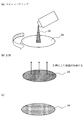
12 支持基材
13 ウエハー
14 接着剤層付きウエハー
21 ウエハー
22 液状接着剤組成物
23 接着剤組成物が塗布されたウエハー
24 接着剤層付きウエハー
31 ウエハー
32 半田バンプ
33 接着剤層
34 接着剤層付きウエハー
35 ダイシングマシン
36 接着剤層付きチップ
37 配線基板
38 電極
39 加熱ステージ
40 電子デバイス
41 配線基板
42 塗布された接着剤組成物
43 Bステージ化された接着剤組成物
44 接着剤付き配線基板
Claims (13)
- (a)ビニル基、マレイミド基、アクリロイル基、メタクリロイル基およびアリル基からなる群から選ばれる1以上の官能基を有するラジカル重合性モノマーと、
(b)極性基を有するポリマーであって、該極性基が、水酸基、カルボキシル基、(メタ)アクリロイル基、およびエポキシ基からなる群より選ばれ、該ポリマーが、10,000ないし1,000,000の範囲内の重量平均分子量を有する、極性基を有するポリマーと、
(c)平均粒径が1μm未満であるフィラーと、
(d)熱ラジカル開始剤と、
を含み、5μm以上100μm以下の厚みを有するフィルム状である、プリアプライドアンダーフィル材用の接着剤組成物。 - (a)ビニル基、マレイミド基、アクリロイル基、メタクリロイル基およびアリル基からなる群から選ばれる1以上の官能基を有するラジカル重合性モノマーと、
(b)極性基を有するポリマーであって、該極性基が、水酸基、カルボキシル基、(メタ)アクリロイル基、およびエポキシ基からなる群より選ばれ、該ポリマーが、10,000ないし1,000,000の範囲内の重量平均分子量を有する、極性基を有するポリマーと、
(c)10ないし80重量%の平均粒径が1μm未満であるフィラーと、
(d)熱ラジカル開始剤と、
を含み、5μm以上100μm以下の厚みを有し、Bステージ化されたフィルム状である、プリアプライドアンダーフィル材用の接着剤組成物。 - 前記(d)熱ラジカル開始剤が有機過酸化物である、請求項1または2に記載の接着剤組成物。
- 支持テープ上に積層された、請求項1ないし3のいずれか一項に記載の接着剤組成物。
- 支持基材上に請求項1または2に記載の接着剤組成物を塗布し、該塗布された接着剤組成物をBステージ化する工程を含む、フィルム状接着剤組成物の製造方法。
- Bステージ化された状態で、ウエハーの素子形成面上に積層された請求項1ないし3のいずれか1項に記載の接着剤組成物を含む、接着剤層付きウエハー。
- さらに、接着剤層上に積層された支持テープを含む、請求項6に記載の接着剤層付きウエハー。
- 請求項1または2に記載の接着剤組成物を、ウエハーの素子形成面上に塗布し、塗布された接着剤組成物をBステージ化する工程を含む、接着剤層付きウエハーの製造方法。
- 請求項1または2に記載のフィルム状接着剤組成物を、ウエハーの素子形成面上に積層する工程を含む、接着剤層付きウエハーの製造方法。
- Bステージ化された状態で配線基板上に積層された請求項1または2に記載の接着剤組成物を含む、接着剤付き配線基板。
- 請求項1に記載の接着剤組成物を配線基板上に塗布し、該塗布された接着剤組成物をBステージ化する工程を含む、接着剤付き配線基板の製造方法。
- 請求項1ないし4のいずれか一項に記載の接着剤組成物を用いて製造された電子デバイス。
- (a)ビニル基、マレイミド基、アクリロイル基、メタクリロイル基およびアリル基からなる群から選ばれる1以上の官能基を有するラジカル重合性モノマーと、
(b)極性基を有するポリマーであって、該極性基が、水酸基、カルボキシル基、(メタ)アクリロイル基、およびエポキシ基からなる群より選ばれ、該ポリマーが、10,000ないし1,000,000の範囲内の重量平均分子量を有する、極性基を有するポリマーと、
(c)平均粒径が1μm未満であるフィラーと、
(d)熱ラジカル開始剤と、
を含み、5μm以上100μm以下の厚みを有し、Bステージ化されたフィルム状である、アンダーフィルフィルムである製品。
Applications Claiming Priority (3)
| Application Number | Priority Date | Filing Date | Title |
|---|---|---|---|
| US201161554698P | 2011-11-02 | 2011-11-02 | |
| US61/554,698 | 2011-11-02 | ||
| PCT/US2012/059961 WO2013066597A1 (en) | 2011-11-02 | 2012-10-12 | Adhesive for electronic component |
Publications (3)
| Publication Number | Publication Date |
|---|---|
| JP2015503220A JP2015503220A (ja) | 2015-01-29 |
| JP2015503220A5 JP2015503220A5 (ja) | 2016-07-14 |
| JP6165754B2 true JP6165754B2 (ja) | 2017-07-19 |
Family
ID=48192591
Family Applications (1)
| Application Number | Title | Priority Date | Filing Date |
|---|---|---|---|
| JP2014539967A Active JP6165754B2 (ja) | 2011-11-02 | 2012-10-12 | 電子部品用接着剤 |
Country Status (6)
| Country | Link |
|---|---|
| US (2) | US9305892B2 (ja) |
| JP (1) | JP6165754B2 (ja) |
| KR (1) | KR101924049B1 (ja) |
| CN (1) | CN104039913B (ja) |
| TW (1) | TWI565778B (ja) |
| WO (1) | WO2013066597A1 (ja) |
Families Citing this family (49)
| Publication number | Priority date | Publication date | Assignee | Title |
|---|---|---|---|---|
| WO2013035205A1 (ja) * | 2011-09-09 | 2013-03-14 | ヘンケル・アクチェンゲゼルシャフト・ウント・コムパニー・コマンディットゲゼルシャフト・アウフ・アクチェン | アンダーフィル用組成物 |
| WO2013035204A1 (ja) * | 2011-09-09 | 2013-03-14 | ヘンケル・アクチェンゲゼルシャフト・ウント・コムパニー・コマンディットゲゼルシャフト・アウフ・アクチェン | 電子装置用組成物 |
| JP5435520B1 (ja) * | 2013-03-29 | 2014-03-05 | 古河電気工業株式会社 | 有機電子デバイス用素子封止用樹脂組成物、有機電子デバイス用素子封止用樹脂シート、有機エレクトロルミネッセンス素子、及び画像表示装置 |
| CN105934478B (zh) | 2014-01-29 | 2020-01-14 | 日立化成株式会社 | 树脂组合物、使用了树脂组合物的半导体装置的制造方法、以及固体摄像元件 |
| TWI660022B (zh) | 2014-01-29 | 2019-05-21 | 日立化成股份有限公司 | 黏著劑組成物、使用黏著劑組成物之半導體裝置的製造方法、及固態成像元件 |
| JP6547632B2 (ja) * | 2014-01-29 | 2019-07-24 | 日立化成株式会社 | 接着剤組成物、接着剤組成物から得られる樹脂硬化物、接着剤組成物を用いた半導体装置の製造方法、及び固体撮像素子 |
| CN106062075B (zh) * | 2014-02-19 | 2019-11-01 | 汉高股份有限及两合公司 | 用于密封液晶的可固化树脂组合物 |
| KR101828644B1 (ko) * | 2014-03-25 | 2018-02-14 | 주식회사 엘지화학 | 방열 점착 테이프용 점착제 조성물 및 방열 점착 테이프 |
| CN104134615A (zh) * | 2014-07-31 | 2014-11-05 | 华进半导体封装先导技术研发中心有限公司 | 铜铜键合的方法 |
| MY179390A (en) * | 2014-08-29 | 2020-11-05 | Furukawa Electric Co Ltd | Maleimide film |
| CN104232014B (zh) * | 2014-09-15 | 2016-02-03 | 东莞市新懿电子材料技术有限公司 | 一种底部填充胶 |
| JP6459402B2 (ja) * | 2014-10-31 | 2019-01-30 | 日立化成株式会社 | 先供給型アンダーフィル材、電子部品装置及び電子部品装置の製造方法 |
| JP6398619B2 (ja) * | 2014-10-31 | 2018-10-03 | 日立化成株式会社 | 先供給型アンダーフィル材、電子部品装置及び電子部品装置の製造方法 |
| DE102015000120A1 (de) * | 2015-01-07 | 2016-07-07 | Merck Patent Gmbh | Elektronisches Bauelement |
| JP6517588B2 (ja) * | 2015-05-27 | 2019-05-22 | デクセリアルズ株式会社 | 熱硬化性接着シート、及び半導体装置の製造方法 |
| JP2017103289A (ja) * | 2015-11-30 | 2017-06-08 | 日立化成株式会社 | 半導体用接着剤、半導体装置、及び半導体装置の製造方法 |
| JP6791626B2 (ja) * | 2015-12-14 | 2020-11-25 | デクセリアルズ株式会社 | 熱硬化性接着シート、及び半導体装置の製造方法 |
| JP6631238B2 (ja) * | 2015-12-22 | 2020-01-15 | 日立化成株式会社 | 先供給型アンダーフィル材、先供給型アンダーフィル材の硬化物、電子部品装置及び電子部品装置の製造方法 |
| JP6707856B2 (ja) * | 2015-12-22 | 2020-06-10 | 日立化成株式会社 | 先供給型アンダーフィル材、電子部品装置の製造方法、及び電子部品装置 |
| JP6638380B2 (ja) * | 2015-12-22 | 2020-01-29 | 日立化成株式会社 | 先供給型アンダーフィル材及びその硬化物、並びに電子部品装置及びその製造方法 |
| JP2017179176A (ja) * | 2016-03-31 | 2017-10-05 | ナミックス株式会社 | フィルム状半導体封止剤、および半導体装置 |
| WO2017209044A1 (ja) | 2016-05-31 | 2017-12-07 | 三菱瓦斯化学株式会社 | 樹脂組成物、積層体、樹脂組成物層付き半導体ウェハ、樹脂組成物層付き半導体搭載用基板及び半導体装置 |
| KR102320303B1 (ko) | 2016-05-31 | 2021-11-02 | 미츠비시 가스 가가쿠 가부시키가이샤 | 수지 조성물, 적층체, 수지 조성물층 부착 반도체 웨이퍼, 수지 조성물층 부착 반도체 탑재용 기판 및 반도체 장치 |
| JP6706995B2 (ja) * | 2016-08-05 | 2020-06-10 | 三井化学東セロ株式会社 | アンダーフィル用絶縁フィルム |
| CN106590502A (zh) * | 2016-12-02 | 2017-04-26 | 陈佩珊 | 用于粘结不同材料的粘合剂组合物 |
| CN110191922A (zh) * | 2017-01-12 | 2019-08-30 | 汉高股份有限及两合公司 | 辐射固化性密封剂组合物 |
| KR101872375B1 (ko) * | 2017-02-13 | 2018-06-29 | 주식회사 로보스타 | 파티클 제거 방법 및 그 장치 |
| US10444101B2 (en) * | 2017-03-06 | 2019-10-15 | Seiko Epson Corporation | Sensor device, force detection device, and robot |
| US11195769B2 (en) | 2017-03-07 | 2021-12-07 | Panasonic Intellectual Property Management Co., Ltd. | Thermosetting composition for use as underfill material, and semiconductor device |
| JP7154037B2 (ja) | 2017-05-16 | 2022-10-17 | デクセリアルズ株式会社 | アンダーフィル材、アンダーフィルフィルム、及びこれを用いた半導体装置の製造方法 |
| JP6920723B2 (ja) | 2017-07-14 | 2021-08-18 | ナミックス株式会社 | 加圧実装用ncf |
| JP7066350B2 (ja) * | 2017-08-03 | 2022-05-13 | 三井化学東セロ株式会社 | 生産性に優れたギャングボンディングプロセス用アンダーフィル絶縁フィルム |
| EP3786233A4 (en) | 2018-04-26 | 2021-12-29 | Mitsubishi Gas Chemical Company, Inc. | Resin composition, laminate, resin composition layer-attached semiconductor wafer, substrate for mounting resin composition layer-attached semiconductor, and semiconductor device |
| TWI808159B (zh) | 2018-04-26 | 2023-07-11 | 日商三菱瓦斯化學股份有限公司 | 樹脂組成物、疊層體、附樹脂組成物層之半導體晶圓、附樹脂組成物層之半導體搭載用基板、以及半導體裝置 |
| EP3790039A4 (en) | 2018-04-26 | 2022-01-19 | Mitsubishi Gas Chemical Company, Inc. | RESIN COMPOSITION, LAMINATE, SEMICONDUCTOR WAFER WITH RESIN COMPOSITION LAYER, SUBSTRATE FOR MOUNTING SEMICONDUCTOR WITH RESIN COMPOSITION LAYER, AND SEMICONDUCTOR DEVICE |
| JP6597845B2 (ja) * | 2018-06-25 | 2019-10-30 | 日立化成株式会社 | 先供給型アンダーフィル材、電子部品装置及び電子部品装置の製造方法 |
| CN112437797A (zh) * | 2018-07-24 | 2021-03-02 | 汉高股份有限及两合公司 | 阻燃粘合剂组合物 |
| EP3992221A4 (en) | 2019-06-28 | 2023-06-21 | Mitsubishi Gas Chemical Company, Inc. | RESIN COMPOSITION, RESIN SHEET, LAMINATE, SEMICONDUCTOR WAFER WITH RESIN COMPOSITION LAYER, SUBSTRATE WITH RESIN COMPOSITION LAYER FOR SEMICONDUCTOR MOUNTING, AND SEMICONDUCTOR DEVICE |
| US20220344227A1 (en) | 2019-06-28 | 2022-10-27 | Mitsubishi Gas Chemical Company, Inc. | Film, laminate, semiconductor wafer with film layer, substrate for mounting a semiconductor with film layer, and semiconductor device |
| EP3991969A4 (en) | 2019-06-28 | 2023-07-19 | Mitsubishi Gas Chemical Company, Inc. | FILM, MULTILAYERY BODY, SEMICONDUCTOR WAFER WITH FILM, SUBSTRATE FOR MOUNTING OF SEMICONDUCTOR WITH FILM AND SEMICONDUCTOR DEVICE |
| EP3992231A4 (en) | 2019-06-28 | 2023-07-05 | Mitsubishi Gas Chemical Company, Inc. | FILM, LAMINATE, SEMICONDUCTOR WAFER WITH FILM LAYER, SEMICONDUCTOR MOUNTING SUBSTRATE WITH FILM LAYER, AND SEMICONDUCTOR DEVICE |
| JP7406336B2 (ja) * | 2019-10-11 | 2023-12-27 | 三星電子株式会社 | 半導体装置の製造方法 |
| JP6844680B2 (ja) * | 2019-12-12 | 2021-03-17 | 昭和電工マテリアルズ株式会社 | 先供給型アンダーフィル材、先供給型アンダーフィル材の硬化物、電子部品装置及び電子部品装置の製造方法 |
| JP6844685B2 (ja) * | 2019-12-26 | 2021-03-17 | 昭和電工マテリアルズ株式会社 | 先供給型アンダーフィル材及びその硬化物、並びに電子部品装置及びその製造方法 |
| WO2021152934A1 (ja) * | 2020-01-29 | 2021-08-05 | 株式会社村田製作所 | 電極付き受動部品及び電極付き受動部品の集合体 |
| GB2593754B (en) | 2020-04-01 | 2022-12-28 | Henkel Ag & Co Kgaa | Redox curable compositions and methods of manufacture thereof |
| FR3113771B1 (fr) * | 2020-08-27 | 2022-10-21 | Commissariat Energie Atomique | Procédé de fabrication d'un substrat-poignée destiné au collage temporaire d'un substrat. |
| CN114316872B (zh) * | 2020-09-29 | 2023-09-05 | 上海飞凯材料科技股份有限公司 | 一种临时粘合剂及其应用和应用方法 |
| CN113427839A (zh) * | 2021-08-26 | 2021-09-24 | 金石(天津)科技发展有限公司 | 复合膜袋及其制备方法 |
Family Cites Families (9)
| Publication number | Priority date | Publication date | Assignee | Title |
|---|---|---|---|---|
| JP3825506B2 (ja) * | 1996-09-02 | 2006-09-27 | Jsr株式会社 | 液状硬化性樹脂組成物 |
| US7144956B2 (en) * | 1998-11-02 | 2006-12-05 | Henkel Corporation | Polymerizable compositions in non-flowable forms |
| JP4883749B2 (ja) * | 2005-02-08 | 2012-02-22 | 日東電工株式会社 | 光学部材用粘着剤組成物、光学部材用粘着剤層およびその製造方法、粘着剤付光学部材、ならびに画像表示装置 |
| KR20120007556A (ko) * | 2007-10-09 | 2012-01-20 | 히다치 가세고교 가부시끼가이샤 | 접착 필름이 부착된 반도체칩의 제조 방법, 이 제조 방법에 사용되는 반도체용 접착 필름, 및 반도체 장치의 제조 방법 |
| JPWO2009128530A1 (ja) * | 2008-04-17 | 2011-08-04 | 日立化成工業株式会社 | 接着剤組成物、回路接続用接着剤、接続体、及び半導体装置 |
| JP6085076B2 (ja) * | 2009-03-16 | 2017-02-22 | リンテック株式会社 | 粘着シートおよび半導体ウエハの加工方法、半導体チップの製造方法 |
| KR20120125491A (ko) * | 2010-01-21 | 2012-11-15 | 세키스이가가쿠 고교가부시키가이샤 | 열경화성 수지 조성물, 플립 칩 실장용 접착제, 반도체 장치의 제조 방법, 및 반도체 장치 |
| KR20120068751A (ko) * | 2010-07-26 | 2012-06-27 | 히다치 가세고교 가부시끼가이샤 | 접착제 조성물, 접속 구조체, 접속 구조체의 제조 방법 및 접착제 조성물의 용도 |
| US9623660B2 (en) * | 2013-05-14 | 2017-04-18 | Xerox Corporation | B-stage film adhesive compatible with aqueous ink for printhead structures interstitial bonding in high density piezo printheads fabrication for aqueous inkjet |
-
2012
- 2012-10-12 WO PCT/US2012/059961 patent/WO2013066597A1/en active Application Filing
- 2012-10-12 KR KR1020147011750A patent/KR101924049B1/ko active IP Right Grant
- 2012-10-12 CN CN201280053590.3A patent/CN104039913B/zh active Active
- 2012-10-12 JP JP2014539967A patent/JP6165754B2/ja active Active
- 2012-10-31 TW TW101140402A patent/TWI565778B/zh active
-
2014
- 2014-05-01 US US14/267,511 patent/US9305892B2/en active Active
-
2016
- 2016-03-10 US US15/066,181 patent/US9780068B2/en active Active
Also Published As
| Publication number | Publication date |
|---|---|
| TW201323558A (zh) | 2013-06-16 |
| US20140242757A1 (en) | 2014-08-28 |
| TWI565778B (zh) | 2017-01-11 |
| CN104039913A (zh) | 2014-09-10 |
| KR20140088543A (ko) | 2014-07-10 |
| US9305892B2 (en) | 2016-04-05 |
| CN104039913B (zh) | 2017-08-22 |
| WO2013066597A1 (en) | 2013-05-10 |
| KR101924049B1 (ko) | 2018-12-03 |
| JP2015503220A (ja) | 2015-01-29 |
| US9780068B2 (en) | 2017-10-03 |
| US20160190094A1 (en) | 2016-06-30 |
Similar Documents
| Publication | Publication Date | Title |
|---|---|---|
| JP6165754B2 (ja) | 電子部品用接着剤 | |
| JP5477144B2 (ja) | 回路部材接続用接着剤シート及び半導体装置の製造方法 | |
| TWI488937B (zh) | Followed by a method of assembling a semiconductor wafer and a semiconductor wafer | |
| JP6429802B2 (ja) | 接着フィルム | |
| TW201134903A (en) | Adhesive composition for a semiconductor device, adhesive film, and dicing die-bonding film | |
| JP5908306B2 (ja) | 半導体接合用接着剤及び半導体接合用接着フィルム | |
| TWI585176B (zh) | 電子裝置用組成物 | |
| JP6514564B2 (ja) | 樹脂組成物、裏面研削用テープ一体型シート状樹脂組成物、ダイシングテープ一体型シート状樹脂組成物、半導体装置の製造方法、及び、半導体装置 | |
| JP6530213B2 (ja) | シート状樹脂組成物、裏面研削用テープ一体型シート状樹脂組成物、及び、半導体装置の製造方法 | |
| JP6084567B2 (ja) | 電子装置用シール剤組成物 | |
| TWI605111B (zh) | 底膠用組成物 | |
| JP7384168B2 (ja) | 半導体装置の製造方法及び半導体ウエハ加工用接着フィルム |
Legal Events
| Date | Code | Title | Description |
|---|---|---|---|
| A621 | Written request for application examination |
Free format text: JAPANESE INTERMEDIATE CODE: A621 Effective date: 20151009 |
|
| A521 | Request for written amendment filed |
Free format text: JAPANESE INTERMEDIATE CODE: A523 Effective date: 20160525 |
|
| A871 | Explanation of circumstances concerning accelerated examination |
Free format text: JAPANESE INTERMEDIATE CODE: A871 Effective date: 20160525 |
|
| A711 | Notification of change in applicant |
Free format text: JAPANESE INTERMEDIATE CODE: A711 Effective date: 20160815 |
|
| A521 | Request for written amendment filed |
Free format text: JAPANESE INTERMEDIATE CODE: A821 Effective date: 20160815 |
|
| A975 | Report on accelerated examination |
Free format text: JAPANESE INTERMEDIATE CODE: A971005 Effective date: 20160901 |
|
| A131 | Notification of reasons for refusal |
Free format text: JAPANESE INTERMEDIATE CODE: A131 Effective date: 20160920 |
|
| A601 | Written request for extension of time |
Free format text: JAPANESE INTERMEDIATE CODE: A601 Effective date: 20161219 |
|
| A521 | Request for written amendment filed |
Free format text: JAPANESE INTERMEDIATE CODE: A523 Effective date: 20170220 |
|
| TRDD | Decision of grant or rejection written | ||
| A01 | Written decision to grant a patent or to grant a registration (utility model) |
Free format text: JAPANESE INTERMEDIATE CODE: A01 Effective date: 20170523 |
|
| A61 | First payment of annual fees (during grant procedure) |
Free format text: JAPANESE INTERMEDIATE CODE: A61 Effective date: 20170621 |
|
| R150 | Certificate of patent or registration of utility model |
Ref document number: 6165754 Country of ref document: JP Free format text: JAPANESE INTERMEDIATE CODE: R150 |
|
| R157 | Certificate of patent or utility model (correction) |
Free format text: JAPANESE INTERMEDIATE CODE: R157 |
|
| R250 | Receipt of annual fees |
Free format text: JAPANESE INTERMEDIATE CODE: R250 |
|
| R250 | Receipt of annual fees |
Free format text: JAPANESE INTERMEDIATE CODE: R250 |
|
| R250 | Receipt of annual fees |
Free format text: JAPANESE INTERMEDIATE CODE: R250 |
|
| S111 | Request for change of ownership or part of ownership |
Free format text: JAPANESE INTERMEDIATE CODE: R313117 |
|
| R350 | Written notification of registration of transfer |
Free format text: JAPANESE INTERMEDIATE CODE: R350 |
|
| R250 | Receipt of annual fees |
Free format text: JAPANESE INTERMEDIATE CODE: R250 |