JP6130199B2 - 半導体装置の駆動方法、プログラム - Google Patents
半導体装置の駆動方法、プログラム Download PDFInfo
- Publication number
- JP6130199B2 JP6130199B2 JP2013091890A JP2013091890A JP6130199B2 JP 6130199 B2 JP6130199 B2 JP 6130199B2 JP 2013091890 A JP2013091890 A JP 2013091890A JP 2013091890 A JP2013091890 A JP 2013091890A JP 6130199 B2 JP6130199 B2 JP 6130199B2
- Authority
- JP
- Japan
- Prior art keywords
- terminal
- transistor
- data
- memory
- error
- Prior art date
- Legal status (The legal status is an assumption and is not a legal conclusion. Google has not performed a legal analysis and makes no representation as to the accuracy of the status listed.)
- Expired - Fee Related
Links
Images


Classifications
-
- G—PHYSICS
- G06—COMPUTING OR CALCULATING; COUNTING
- G06F—ELECTRIC DIGITAL DATA PROCESSING
- G06F11/00—Error detection; Error correction; Monitoring
- G06F11/07—Responding to the occurrence of a fault, e.g. fault tolerance
- G06F11/08—Error detection or correction by redundancy in data representation, e.g. by using checking codes
- G06F11/10—Adding special bits or symbols to the coded information, e.g. parity check, casting out 9's or 11's
- G06F11/1004—Adding special bits or symbols to the coded information, e.g. parity check, casting out 9's or 11's to protect a block of data words, e.g. CRC or checksum
-
- G—PHYSICS
- G06—COMPUTING OR CALCULATING; COUNTING
- G06F—ELECTRIC DIGITAL DATA PROCESSING
- G06F3/00—Input arrangements for transferring data to be processed into a form capable of being handled by the computer; Output arrangements for transferring data from processing unit to output unit, e.g. interface arrangements
- G06F3/06—Digital input from, or digital output to, record carriers, e.g. RAID, emulated record carriers or networked record carriers
- G06F3/0601—Interfaces specially adapted for storage systems
- G06F3/0602—Interfaces specially adapted for storage systems specifically adapted to achieve a particular effect
- G06F3/0614—Improving the reliability of storage systems
- G06F3/0619—Improving the reliability of storage systems in relation to data integrity, e.g. data losses, bit errors
-
- G—PHYSICS
- G06—COMPUTING OR CALCULATING; COUNTING
- G06F—ELECTRIC DIGITAL DATA PROCESSING
- G06F3/00—Input arrangements for transferring data to be processed into a form capable of being handled by the computer; Output arrangements for transferring data from processing unit to output unit, e.g. interface arrangements
- G06F3/06—Digital input from, or digital output to, record carriers, e.g. RAID, emulated record carriers or networked record carriers
- G06F3/0601—Interfaces specially adapted for storage systems
- G06F3/0628—Interfaces specially adapted for storage systems making use of a particular technique
- G06F3/0638—Organizing or formatting or addressing of data
- G06F3/064—Management of blocks
-
- G—PHYSICS
- G06—COMPUTING OR CALCULATING; COUNTING
- G06F—ELECTRIC DIGITAL DATA PROCESSING
- G06F3/00—Input arrangements for transferring data to be processed into a form capable of being handled by the computer; Output arrangements for transferring data from processing unit to output unit, e.g. interface arrangements
- G06F3/06—Digital input from, or digital output to, record carriers, e.g. RAID, emulated record carriers or networked record carriers
- G06F3/0601—Interfaces specially adapted for storage systems
- G06F3/0668—Interfaces specially adapted for storage systems adopting a particular infrastructure
- G06F3/0671—In-line storage system
- G06F3/0673—Single storage device
- G06F3/0679—Non-volatile semiconductor memory device, e.g. flash memory, one time programmable memory [OTP]
-
- G—PHYSICS
- G11—INFORMATION STORAGE
- G11C—STATIC STORES
- G11C11/00—Digital stores characterised by the use of particular electric or magnetic storage elements; Storage elements therefor
- G11C11/21—Digital stores characterised by the use of particular electric or magnetic storage elements; Storage elements therefor using electric elements
- G11C11/34—Digital stores characterised by the use of particular electric or magnetic storage elements; Storage elements therefor using electric elements using semiconductor devices
- G11C11/40—Digital stores characterised by the use of particular electric or magnetic storage elements; Storage elements therefor using electric elements using semiconductor devices using transistors
- G11C11/401—Digital stores characterised by the use of particular electric or magnetic storage elements; Storage elements therefor using electric elements using semiconductor devices using transistors forming cells needing refreshing or charge regeneration, i.e. dynamic cells
- G11C11/403—Digital stores characterised by the use of particular electric or magnetic storage elements; Storage elements therefor using electric elements using semiconductor devices using transistors forming cells needing refreshing or charge regeneration, i.e. dynamic cells with charge regeneration common to a multiplicity of memory cells, i.e. external refresh
- G11C11/405—Digital stores characterised by the use of particular electric or magnetic storage elements; Storage elements therefor using electric elements using semiconductor devices using transistors forming cells needing refreshing or charge regeneration, i.e. dynamic cells with charge regeneration common to a multiplicity of memory cells, i.e. external refresh with three charge-transfer gates, e.g. MOS transistors, per cell
-
- G—PHYSICS
- G11—INFORMATION STORAGE
- G11C—STATIC STORES
- G11C16/00—Erasable programmable read-only memories
- G11C16/02—Erasable programmable read-only memories electrically programmable
- G11C16/04—Erasable programmable read-only memories electrically programmable using variable threshold transistors, e.g. FAMOS
- G11C16/0408—Erasable programmable read-only memories electrically programmable using variable threshold transistors, e.g. FAMOS comprising cells containing floating gate transistors
- G11C16/0416—Erasable programmable read-only memories electrically programmable using variable threshold transistors, e.g. FAMOS comprising cells containing floating gate transistors comprising cells containing a single floating gate transistor and no select transistor, e.g. UV EPROM
-
- G—PHYSICS
- G11—INFORMATION STORAGE
- G11C—STATIC STORES
- G11C16/00—Erasable programmable read-only memories
- G11C16/02—Erasable programmable read-only memories electrically programmable
- G11C16/04—Erasable programmable read-only memories electrically programmable using variable threshold transistors, e.g. FAMOS
- G11C16/0408—Erasable programmable read-only memories electrically programmable using variable threshold transistors, e.g. FAMOS comprising cells containing floating gate transistors
- G11C16/0433—Erasable programmable read-only memories electrically programmable using variable threshold transistors, e.g. FAMOS comprising cells containing floating gate transistors comprising cells containing a single floating gate transistor and one or more separate select transistors
-
- G—PHYSICS
- G11—INFORMATION STORAGE
- G11C—STATIC STORES
- G11C29/00—Checking stores for correct operation ; Subsequent repair; Testing stores during standby or offline operation
- G11C29/04—Detection or location of defective memory elements, e.g. cell constructio details, timing of test signals
-
- G—PHYSICS
- G11—INFORMATION STORAGE
- G11C—STATIC STORES
- G11C29/00—Checking stores for correct operation ; Subsequent repair; Testing stores during standby or offline operation
- G11C29/52—Protection of memory contents; Detection of errors in memory contents
-
- H—ELECTRICITY
- H10—SEMICONDUCTOR DEVICES; ELECTRIC SOLID-STATE DEVICES NOT OTHERWISE PROVIDED FOR
- H10D—INORGANIC ELECTRIC SEMICONDUCTOR DEVICES
- H10D86/00—Integrated devices formed in or on insulating or conducting substrates, e.g. formed in silicon-on-insulator [SOI] substrates or on stainless steel or glass substrates
- H10D86/40—Integrated devices formed in or on insulating or conducting substrates, e.g. formed in silicon-on-insulator [SOI] substrates or on stainless steel or glass substrates characterised by multiple TFTs
- H10D86/60—Integrated devices formed in or on insulating or conducting substrates, e.g. formed in silicon-on-insulator [SOI] substrates or on stainless steel or glass substrates characterised by multiple TFTs wherein the TFTs are in active matrices
-
- G—PHYSICS
- G11—INFORMATION STORAGE
- G11C—STATIC STORES
- G11C16/00—Erasable programmable read-only memories
- G11C16/02—Erasable programmable read-only memories electrically programmable
- G11C16/04—Erasable programmable read-only memories electrically programmable using variable threshold transistors, e.g. FAMOS
- G11C16/0408—Erasable programmable read-only memories electrically programmable using variable threshold transistors, e.g. FAMOS comprising cells containing floating gate transistors
- G11C16/0441—Erasable programmable read-only memories electrically programmable using variable threshold transistors, e.g. FAMOS comprising cells containing floating gate transistors comprising cells containing multiple floating gate devices, e.g. separate read-and-write FAMOS transistors with connected floating gates
- G11C16/045—Floating gate memory cells with both P and N channel memory transistors, usually sharing a common floating gate
-
- G—PHYSICS
- G11—INFORMATION STORAGE
- G11C—STATIC STORES
- G11C29/00—Checking stores for correct operation ; Subsequent repair; Testing stores during standby or offline operation
- G11C29/04—Detection or location of defective memory elements, e.g. cell constructio details, timing of test signals
- G11C2029/0409—Online test
-
- G—PHYSICS
- G11—INFORMATION STORAGE
- G11C—STATIC STORES
- G11C29/00—Checking stores for correct operation ; Subsequent repair; Testing stores during standby or offline operation
- G11C29/04—Detection or location of defective memory elements, e.g. cell constructio details, timing of test signals
- G11C2029/0411—Online error correction
Landscapes
- Engineering & Computer Science (AREA)
- Microelectronics & Electronic Packaging (AREA)
- Theoretical Computer Science (AREA)
- General Engineering & Computer Science (AREA)
- Physics & Mathematics (AREA)
- General Physics & Mathematics (AREA)
- Computer Security & Cryptography (AREA)
- Human Computer Interaction (AREA)
- Quality & Reliability (AREA)
- Computer Hardware Design (AREA)
- Dram (AREA)
- For Increasing The Reliability Of Semiconductor Memories (AREA)
- Semiconductor Memories (AREA)
- Logic Circuits (AREA)
Description
本発明の一態様である半導体装置に適用可能なメモリ素子の構成とその動作を説明する。
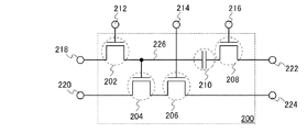
図2には、本発明の一態様である半導体装置に適用可能なメモリ素子の一構成例であって、図1(A)及び(B)とは異なる形態を示す。図2に示すメモリ素子200は、第1のトランジスタ202と、第2のトランジスタ204と、第3のトランジスタ206と、第4のトランジスタ208と、容量素子210と、データ保持部226と、を有し、第1の端子212、第2の端子214、第3の端子216、第4の端子218、第5の端子220、第6の端子222及び第7の端子224に電気的に接続されている。
実施の形態1で説明したメモリ素子100、メモリ素子150及び実施の形態2で説明したメモリ素子200では、データを読み出す前に、少なくとも2つの端子間で電位を異なるものとしておくこと(プリチャージ動作)が必要である。例えば、図1(A)のメモリ素子100では、第4の端子114と第5の端子116の電位を互いに異なるものとすることが必要である。
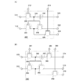
次に、本発明の一態様であるCRCを行う半導体装置の駆動方法について説明する。図4(A)には、本発明の一態様である半導体装置の駆動方法に用いるコンフィギュレーションメモリ400とCRC用メモリ402を示している。図4(A)によれば、コンフィギュレーションメモリのそれぞれの行には、対応するCRC用メモリを有する。CRC用メモリ402は、行数×CRCのビット数の容量を要する。すなわち、図4(A)に示す構成ではCRCのビット数が8ビットであるため、CRC用メモリには、256×8=2048ビットの容量が必要である。なお、CRCのビット数は8ビットに限定されるものではないことを注記する。
102 第1のトランジスタ
104 第2のトランジスタ
106 容量素子
108 第1の端子
110 第2の端子
112 第3の端子
114 第4の端子
116 第5の端子
118 データ保持部
150 メモリ素子
152 第1のトランジスタ
154 第2のトランジスタ
156 第3のトランジスタ
158 容量素子
160 第1の端子
162 第2の端子
164 第3の端子
166 第4の端子
168 第5の端子
170 第6の端子
172 データ保持部
200 メモリ素子
202 第1のトランジスタ
204 第2のトランジスタ
206 第3のトランジスタ
208 第4のトランジスタ
210 容量素子
212 第1の端子
214 第2の端子
216 第3の端子
218 第4の端子
220 第5の端子
222 第6の端子
224 第7の端子
226 データ保持部
300 メモリ素子
302 第1のトランジスタ
304 第2のトランジスタ
306 第3のトランジスタ
308 第4のトランジスタ
310 容量素子
312 第1の端子
314 第2の端子
316 第3の端子
318 第4の端子
320 第5の端子
322 第6の端子
324 第7の端子
326 データ保持部
350 メモリ素子
352 第1のトランジスタ
354 第2のトランジスタ
356 第3のトランジスタ
358 第4のトランジスタ
360 第5のトランジスタ
362 容量素子
364 第1の端子
366 第2の端子
368 第3の端子
370 第4の端子
372 第5の端子
374 第6の端子
376 第7の端子
378 第8の端子
380 データ保持部
400 コンフィギュレーションメモリ
402 CRC用メモリ
404 データ入出力回路
406 CRC演算回路
408 ブートメモリ
410 入力レジスタ
412 除数レジスタ
414 演算回路
416 桁数カウンタ
500 開始
502 ループ開始
504 第i行の剰余値計算
506 第i行のデータ書き込み
508 第i行のエラー判定
510 ループ終了
512 処理の移行
600 ユーザーモードの開始
602 ループ開始
604 「k=1」
606 第i行のエラー判定
608 第i行のデータ書き込み
610 「k+1」
612 「k=mの判定」
614 第i行の剰余値計算
616 第i行のデータ書き込み
618 第i行のエラー判定
620 ループ終了
622 終了
Claims (2)
- 巡回冗長検査によりエラー判定を行うに際し、コンフィギュレーションメモリと剰余値が記憶されたメモリを用いる半導体装置の駆動方法であって、
予め算出された前記剰余値を用いて第i行のエラー判定を行い、
前記第i行にエラーがない場合には第i+1行の処理に移行し、
前記第i行にエラーがある場合にはコンフィギュレーションメモリに記憶された第i行に入力すべきデータの書き込みを行い、
前記エラー判定と前記データの書き込みを前記エラー判定によりエラーが検出されなくなるまで繰り返し、
前記巡回冗長検査に用いる前記剰余値は、前記コンフィギュレーションメモリよりもエラー率の低いメモリ素子に記憶されていることを特徴とする半導体装置の駆動方法。 - 請求項1に記載の半導体装置の駆動方法を実行させるプログラム。
Priority Applications (1)
| Application Number | Priority Date | Filing Date | Title |
|---|---|---|---|
| JP2013091890A JP6130199B2 (ja) | 2012-04-25 | 2013-04-25 | 半導体装置の駆動方法、プログラム |
Applications Claiming Priority (3)
| Application Number | Priority Date | Filing Date | Title |
|---|---|---|---|
| JP2012100190 | 2012-04-25 | ||
| JP2012100190 | 2012-04-25 | ||
| JP2013091890A JP6130199B2 (ja) | 2012-04-25 | 2013-04-25 | 半導体装置の駆動方法、プログラム |
Publications (3)
| Publication Number | Publication Date |
|---|---|
| JP2013242956A JP2013242956A (ja) | 2013-12-05 |
| JP2013242956A5 JP2013242956A5 (ja) | 2016-06-16 |
| JP6130199B2 true JP6130199B2 (ja) | 2017-05-17 |
Family
ID=49477150
Family Applications (1)
| Application Number | Title | Priority Date | Filing Date |
|---|---|---|---|
| JP2013091890A Expired - Fee Related JP6130199B2 (ja) | 2012-04-25 | 2013-04-25 | 半導体装置の駆動方法、プログラム |
Country Status (3)
| Country | Link |
|---|---|
| US (2) | US9230683B2 (ja) |
| JP (1) | JP6130199B2 (ja) |
| KR (1) | KR102103607B1 (ja) |
Cited By (1)
| Publication number | Priority date | Publication date | Assignee | Title |
|---|---|---|---|---|
| US10018735B2 (en) | 2013-07-17 | 2018-07-10 | Koninklijke Philips N.V. | CE3+ activated luminescent compositions for application in imaging systems |
Families Citing this family (25)
| Publication number | Priority date | Publication date | Assignee | Title |
|---|---|---|---|---|
| CN104321967B (zh) | 2012-05-25 | 2018-01-09 | 株式会社半导体能源研究所 | 可编程逻辑装置及半导体装置 |
| JP6377317B2 (ja) | 2012-05-30 | 2018-08-22 | 株式会社半導体エネルギー研究所 | プログラマブルロジックデバイス |
| TWI621337B (zh) | 2013-05-14 | 2018-04-11 | 半導體能源研究所股份有限公司 | 信號處理裝置 |
| TWI641112B (zh) | 2013-06-13 | 2018-11-11 | 半導體能源研究所股份有限公司 | 半導體裝置 |
| JP6368155B2 (ja) | 2013-06-18 | 2018-08-01 | 株式会社半導体エネルギー研究所 | プログラマブルロジックデバイス |
| JP6483402B2 (ja) | 2013-11-01 | 2019-03-13 | 株式会社半導体エネルギー研究所 | 記憶装置、及び記憶装置を有する電子機器 |
| JP6478562B2 (ja) | 2013-11-07 | 2019-03-06 | 株式会社半導体エネルギー研究所 | 半導体装置 |
| JP6393590B2 (ja) | 2013-11-22 | 2018-09-19 | 株式会社半導体エネルギー研究所 | 半導体装置 |
| JP6444723B2 (ja) | 2014-01-09 | 2018-12-26 | 株式会社半導体エネルギー研究所 | 装置 |
| US9379713B2 (en) | 2014-01-17 | 2016-06-28 | Semiconductor Energy Laboratory Co., Ltd. | Data processing device and driving method thereof |
| JP6521643B2 (ja) | 2014-01-24 | 2019-05-29 | 株式会社半導体エネルギー研究所 | 半導体装置 |
| US9721968B2 (en) | 2014-02-06 | 2017-08-01 | Semiconductor Energy Laboratory Co., Ltd. | Semiconductor device, electronic component, and electronic appliance |
| US9869716B2 (en) | 2014-02-07 | 2018-01-16 | Semiconductor Energy Laboratory Co., Ltd. | Device comprising programmable logic element |
| JP2015165226A (ja) | 2014-02-07 | 2015-09-17 | 株式会社半導体エネルギー研究所 | 装置 |
| WO2015118436A1 (en) | 2014-02-07 | 2015-08-13 | Semiconductor Energy Laboratory Co., Ltd. | Semiconductor device, device, and electronic device |
| JP6442321B2 (ja) | 2014-03-07 | 2018-12-19 | 株式会社半導体エネルギー研究所 | 半導体装置及びその駆動方法、並びに電子機器 |
| US9419622B2 (en) | 2014-03-07 | 2016-08-16 | Semiconductor Energy Laboratory Co., Ltd. | Semiconductor device |
| JP6541376B2 (ja) | 2014-03-13 | 2019-07-10 | 株式会社半導体エネルギー研究所 | プログラマブルロジックデバイスの動作方法 |
| JP6423858B2 (ja) * | 2014-03-14 | 2018-11-14 | 株式会社半導体エネルギー研究所 | 半導体装置、電子部品、及び電子機器 |
| TWI643457B (zh) * | 2014-04-25 | 2018-12-01 | 日商半導體能源研究所股份有限公司 | 半導體裝置 |
| KR102643895B1 (ko) | 2015-10-30 | 2024-03-05 | 가부시키가이샤 한도오따이 에네루기 켄큐쇼 | 반도체 장치, 전자 부품, 및 전자 기기 |
| US9998119B2 (en) | 2016-05-20 | 2018-06-12 | Semiconductor Energy Laboratory Co., Ltd. | Semiconductor device, electronic component, and electronic device |
| US10552258B2 (en) | 2016-09-16 | 2020-02-04 | Semiconductor Energy Laboratory Co., Ltd. | Semiconductor device, electronic device, and driving method thereof |
| DE102017221343A1 (de) | 2017-11-28 | 2019-05-29 | Sirona Dental Systems Gmbh | Zahnersatzformblock und Verfahren zur Herstellung eines Zahnersatzteils aus dem Zahnersatzformblock |
| US11081203B2 (en) * | 2019-11-14 | 2021-08-03 | Micron Technology, Inc. | Leakage source detection by scanning access lines |
Family Cites Families (121)
| Publication number | Priority date | Publication date | Assignee | Title |
|---|---|---|---|---|
| JPS60198861A (ja) | 1984-03-23 | 1985-10-08 | Fujitsu Ltd | 薄膜トランジスタ |
| JPH0244256B2 (ja) | 1987-01-28 | 1990-10-03 | Kagaku Gijutsucho Mukizaishitsu Kenkyushocho | Ingazn2o5deshimesarerurotsuhoshokeinosojokozoojusurukagobutsuoyobisonoseizoho |
| JPH0244258B2 (ja) | 1987-02-24 | 1990-10-03 | Kagaku Gijutsucho Mukizaishitsu Kenkyushocho | Ingazn3o6deshimesarerurotsuhoshokeinosojokozoojusurukagobutsuoyobisonoseizoho |
| JPS63210023A (ja) | 1987-02-24 | 1988-08-31 | Natl Inst For Res In Inorg Mater | InGaZn↓4O↓7で示される六方晶系の層状構造を有する化合物およびその製造法 |
| JPH0244260B2 (ja) | 1987-02-24 | 1990-10-03 | Kagaku Gijutsucho Mukizaishitsu Kenkyushocho | Ingazn5o8deshimesarerurotsuhoshokeinosojokozoojusurukagobutsuoyobisonoseizoho |
| JPH0244262B2 (ja) | 1987-02-27 | 1990-10-03 | Kagaku Gijutsucho Mukizaishitsu Kenkyushocho | Ingazn6o9deshimesarerurotsuhoshokeinosojokozoojusurukagobutsuoyobisonoseizoho |
| JPH0244263B2 (ja) | 1987-04-22 | 1990-10-03 | Kagaku Gijutsucho Mukizaishitsu Kenkyushocho | Ingazn7o10deshimesarerurotsuhoshokeinosojokozoojusurukagobutsuoyobisonoseizoho |
| JPH05251705A (ja) | 1992-03-04 | 1993-09-28 | Fuji Xerox Co Ltd | 薄膜トランジスタ |
| JP3479375B2 (ja) | 1995-03-27 | 2003-12-15 | 科学技術振興事業団 | 亜酸化銅等の金属酸化物半導体による薄膜トランジスタとpn接合を形成した金属酸化物半導体装置およびそれらの製造方法 |
| JPH11505377A (ja) | 1995-08-03 | 1999-05-18 | フィリップス エレクトロニクス ネムローゼ フェンノートシャップ | 半導体装置 |
| JP3625598B2 (ja) | 1995-12-30 | 2005-03-02 | 三星電子株式会社 | 液晶表示装置の製造方法 |
| US6237124B1 (en) * | 1998-03-16 | 2001-05-22 | Actel Corporation | Methods for errors checking the configuration SRAM and user assignable SRAM data in a field programmable gate array |
| JP4170454B2 (ja) | 1998-07-24 | 2008-10-22 | Hoya株式会社 | 透明導電性酸化物薄膜を有する物品及びその製造方法 |
| JP2000150861A (ja) | 1998-11-16 | 2000-05-30 | Tdk Corp | 酸化物薄膜 |
| JP3276930B2 (ja) | 1998-11-17 | 2002-04-22 | 科学技術振興事業団 | トランジスタ及び半導体装置 |
| TW460731B (en) | 1999-09-03 | 2001-10-21 | Ind Tech Res Inst | Electrode structure and production method of wide viewing angle LCD |
| JP4089858B2 (ja) | 2000-09-01 | 2008-05-28 | 国立大学法人東北大学 | 半導体デバイス |
| KR20020038482A (ko) | 2000-11-15 | 2002-05-23 | 모리시타 요이찌 | 박막 트랜지스터 어레이, 그 제조방법 및 그것을 이용한표시패널 |
| US6700827B2 (en) * | 2001-02-08 | 2004-03-02 | Integrated Device Technology, Inc. | Cam circuit with error correction |
| JP3997731B2 (ja) | 2001-03-19 | 2007-10-24 | 富士ゼロックス株式会社 | 基材上に結晶性半導体薄膜を形成する方法 |
| JP2002289859A (ja) | 2001-03-23 | 2002-10-04 | Minolta Co Ltd | 薄膜トランジスタ |
| JP4090716B2 (ja) | 2001-09-10 | 2008-05-28 | 雅司 川崎 | 薄膜トランジスタおよびマトリクス表示装置 |
| JP3925839B2 (ja) | 2001-09-10 | 2007-06-06 | シャープ株式会社 | 半導体記憶装置およびその試験方法 |
| CN100489797C (zh) | 2001-10-11 | 2009-05-20 | 阿尔特拉公司 | 可编程逻辑设备上的错误检测 |
| JP4164562B2 (ja) | 2002-09-11 | 2008-10-15 | 独立行政法人科学技術振興機構 | ホモロガス薄膜を活性層として用いる透明薄膜電界効果型トランジスタ |
| EP1443130B1 (en) | 2001-11-05 | 2011-09-28 | Japan Science and Technology Agency | Natural superlattice homologous single crystal thin film, method for preparation thereof, and device using said single crystal thin film |
| JP4083486B2 (ja) | 2002-02-21 | 2008-04-30 | 独立行政法人科学技術振興機構 | LnCuO(S,Se,Te)単結晶薄膜の製造方法 |
| US7049190B2 (en) | 2002-03-15 | 2006-05-23 | Sanyo Electric Co., Ltd. | Method for forming ZnO film, method for forming ZnO semiconductor layer, method for fabricating semiconductor device, and semiconductor device |
| JP3933591B2 (ja) | 2002-03-26 | 2007-06-20 | 淳二 城戸 | 有機エレクトロルミネッセント素子 |
| US6735110B1 (en) | 2002-04-17 | 2004-05-11 | Xilinx, Inc. | Memory cells enhanced for resistance to single event upset |
| US7339187B2 (en) | 2002-05-21 | 2008-03-04 | State Of Oregon Acting By And Through The Oregon State Board Of Higher Education On Behalf Of Oregon State University | Transistor structures |
| JP2004022625A (ja) | 2002-06-13 | 2004-01-22 | Murata Mfg Co Ltd | 半導体デバイス及び該半導体デバイスの製造方法 |
| US7105868B2 (en) | 2002-06-24 | 2006-09-12 | Cermet, Inc. | High-electron mobility transistor with zinc oxide |
| US7067843B2 (en) | 2002-10-11 | 2006-06-27 | E. I. Du Pont De Nemours And Company | Transparent oxide semiconductor thin film transistors |
| JP4166105B2 (ja) | 2003-03-06 | 2008-10-15 | シャープ株式会社 | 半導体装置およびその製造方法 |
| JP2004273732A (ja) | 2003-03-07 | 2004-09-30 | Sharp Corp | アクティブマトリクス基板およびその製造方法 |
| US6876572B2 (en) | 2003-05-21 | 2005-04-05 | Altera Corporation | Programmable logic devices with stabilized configuration cells for reduced soft error rates |
| JP4108633B2 (ja) | 2003-06-20 | 2008-06-25 | シャープ株式会社 | 薄膜トランジスタおよびその製造方法ならびに電子デバイス |
| US7262463B2 (en) | 2003-07-25 | 2007-08-28 | Hewlett-Packard Development Company, L.P. | Transistor including a deposited channel region having a doped portion |
| US7023744B1 (en) * | 2003-11-18 | 2006-04-04 | Xilinx, Inc. | Reconfigurable SRAM-ROM cell |
| US7254800B1 (en) * | 2004-02-26 | 2007-08-07 | Xilinx, Inc. | Methods of providing error correction in configuration bitstreams for programmable logic devices |
| US7088606B2 (en) * | 2004-03-10 | 2006-08-08 | Altera Corporation | Dynamic RAM storage techniques |
| US7145174B2 (en) | 2004-03-12 | 2006-12-05 | Hewlett-Packard Development Company, Lp. | Semiconductor device |
| EP1737044B1 (en) | 2004-03-12 | 2014-12-10 | Japan Science and Technology Agency | Amorphous oxide and thin film transistor |
| US7297977B2 (en) | 2004-03-12 | 2007-11-20 | Hewlett-Packard Development Company, L.P. | Semiconductor device |
| US7282782B2 (en) | 2004-03-12 | 2007-10-16 | Hewlett-Packard Development Company, L.P. | Combined binary oxide semiconductor device |
| US7211825B2 (en) | 2004-06-14 | 2007-05-01 | Yi-Chi Shih | Indium oxide-based thin film transistors and circuits |
| US7319253B2 (en) | 2004-07-01 | 2008-01-15 | Altera Corporation | Integrated circuit structures for increasing resistance to single event upset |
| JP2006100760A (ja) | 2004-09-02 | 2006-04-13 | Casio Comput Co Ltd | 薄膜トランジスタおよびその製造方法 |
| US7285501B2 (en) | 2004-09-17 | 2007-10-23 | Hewlett-Packard Development Company, L.P. | Method of forming a solution processed device |
| US7298084B2 (en) | 2004-11-02 | 2007-11-20 | 3M Innovative Properties Company | Methods and displays utilizing integrated zinc oxide row and column drivers in conjunction with organic light emitting diodes |
| EP1815530B1 (en) | 2004-11-10 | 2021-02-17 | Canon Kabushiki Kaisha | Field effect transistor employing an amorphous oxide |
| KR100998527B1 (ko) | 2004-11-10 | 2010-12-07 | 고쿠리츠다이가쿠호진 토쿄고교 다이가꾸 | 비정질 산화물 및 전계 효과 트랜지스터 |
| US7863611B2 (en) | 2004-11-10 | 2011-01-04 | Canon Kabushiki Kaisha | Integrated circuits utilizing amorphous oxides |
| US7791072B2 (en) | 2004-11-10 | 2010-09-07 | Canon Kabushiki Kaisha | Display |
| US7453065B2 (en) | 2004-11-10 | 2008-11-18 | Canon Kabushiki Kaisha | Sensor and image pickup device |
| RU2358354C2 (ru) | 2004-11-10 | 2009-06-10 | Кэнон Кабусики Кайся | Светоизлучающее устройство |
| US7829444B2 (en) | 2004-11-10 | 2010-11-09 | Canon Kabushiki Kaisha | Field effect transistor manufacturing method |
| US7579224B2 (en) | 2005-01-21 | 2009-08-25 | Semiconductor Energy Laboratory Co., Ltd. | Method for manufacturing a thin film semiconductor device |
| TWI481024B (zh) | 2005-01-28 | 2015-04-11 | 半導體能源研究所股份有限公司 | 半導體裝置,電子裝置,和半導體裝置的製造方法 |
| TWI505473B (zh) | 2005-01-28 | 2015-10-21 | 半導體能源研究所股份有限公司 | 半導體裝置,電子裝置,和半導體裝置的製造方法 |
| US7858451B2 (en) | 2005-02-03 | 2010-12-28 | Semiconductor Energy Laboratory Co., Ltd. | Electronic device, semiconductor device and manufacturing method thereof |
| US7948171B2 (en) | 2005-02-18 | 2011-05-24 | Semiconductor Energy Laboratory Co., Ltd. | Light emitting device |
| US20060197092A1 (en) | 2005-03-03 | 2006-09-07 | Randy Hoffman | System and method for forming conductive material on a substrate |
| US8681077B2 (en) | 2005-03-18 | 2014-03-25 | Semiconductor Energy Laboratory Co., Ltd. | Semiconductor device, and display device, driving method and electronic apparatus thereof |
| US7544967B2 (en) | 2005-03-28 | 2009-06-09 | Massachusetts Institute Of Technology | Low voltage flexible organic/transparent transistor for selective gas sensing, photodetecting and CMOS device applications |
| US7645478B2 (en) | 2005-03-31 | 2010-01-12 | 3M Innovative Properties Company | Methods of making displays |
| US8300031B2 (en) | 2005-04-20 | 2012-10-30 | Semiconductor Energy Laboratory Co., Ltd. | Semiconductor device comprising transistor having gate and drain connected through a current-voltage conversion element |
| US7620876B2 (en) | 2005-06-08 | 2009-11-17 | Altera Corporation | Reducing false positives in configuration error detection for programmable devices |
| JP2006344849A (ja) | 2005-06-10 | 2006-12-21 | Casio Comput Co Ltd | 薄膜トランジスタ |
| US7691666B2 (en) | 2005-06-16 | 2010-04-06 | Eastman Kodak Company | Methods of making thin film transistors comprising zinc-oxide-based semiconductor materials and transistors made thereby |
| US7402506B2 (en) | 2005-06-16 | 2008-07-22 | Eastman Kodak Company | Methods of making thin film transistors comprising zinc-oxide-based semiconductor materials and transistors made thereby |
| US7507618B2 (en) | 2005-06-27 | 2009-03-24 | 3M Innovative Properties Company | Method for making electronic devices using metal oxide nanoparticles |
| KR100711890B1 (ko) | 2005-07-28 | 2007-04-25 | 삼성에스디아이 주식회사 | 유기 발광표시장치 및 그의 제조방법 |
| JP2007059128A (ja) | 2005-08-23 | 2007-03-08 | Canon Inc | 有機el表示装置およびその製造方法 |
| JP2007073705A (ja) | 2005-09-06 | 2007-03-22 | Canon Inc | 酸化物半導体チャネル薄膜トランジスタおよびその製造方法 |
| JP4280736B2 (ja) | 2005-09-06 | 2009-06-17 | キヤノン株式会社 | 半導体素子 |
| JP4850457B2 (ja) | 2005-09-06 | 2012-01-11 | キヤノン株式会社 | 薄膜トランジスタ及び薄膜ダイオード |
| JP5116225B2 (ja) | 2005-09-06 | 2013-01-09 | キヤノン株式会社 | 酸化物半導体デバイスの製造方法 |
| EP1998373A3 (en) | 2005-09-29 | 2012-10-31 | Semiconductor Energy Laboratory Co, Ltd. | Semiconductor device having oxide semiconductor layer and manufacturing method thereof |
| JP5037808B2 (ja) | 2005-10-20 | 2012-10-03 | キヤノン株式会社 | アモルファス酸化物を用いた電界効果型トランジスタ、及び該トランジスタを用いた表示装置 |
| CN101577231B (zh) | 2005-11-15 | 2013-01-02 | 株式会社半导体能源研究所 | 半导体器件及其制造方法 |
| TWI292281B (en) | 2005-12-29 | 2008-01-01 | Ind Tech Res Inst | Pixel structure of active organic light emitting diode and method of fabricating the same |
| US7867636B2 (en) | 2006-01-11 | 2011-01-11 | Murata Manufacturing Co., Ltd. | Transparent conductive film and method for manufacturing the same |
| JP4977478B2 (ja) | 2006-01-21 | 2012-07-18 | 三星電子株式会社 | ZnOフィルム及びこれを用いたTFTの製造方法 |
| US7576394B2 (en) | 2006-02-02 | 2009-08-18 | Kochi Industrial Promotion Center | Thin film transistor including low resistance conductive thin films and manufacturing method thereof |
| US7977169B2 (en) | 2006-02-15 | 2011-07-12 | Kochi Industrial Promotion Center | Semiconductor device including active layer made of zinc oxide with controlled orientations and manufacturing method thereof |
| KR20070101595A (ko) | 2006-04-11 | 2007-10-17 | 삼성전자주식회사 | ZnO TFT |
| US7702978B2 (en) * | 2006-04-21 | 2010-04-20 | Altera Corporation | Soft error location and sensitivity detection for programmable devices |
| US20070252928A1 (en) | 2006-04-28 | 2007-11-01 | Toppan Printing Co., Ltd. | Structure, transmission type liquid crystal display, reflection type display and manufacturing method thereof |
| JP5028033B2 (ja) | 2006-06-13 | 2012-09-19 | キヤノン株式会社 | 酸化物半導体膜のドライエッチング方法 |
| JP4999400B2 (ja) | 2006-08-09 | 2012-08-15 | キヤノン株式会社 | 酸化物半導体膜のドライエッチング方法 |
| JP4609797B2 (ja) | 2006-08-09 | 2011-01-12 | Nec液晶テクノロジー株式会社 | 薄膜デバイス及びその製造方法 |
| JP4332545B2 (ja) | 2006-09-15 | 2009-09-16 | キヤノン株式会社 | 電界効果型トランジスタ及びその製造方法 |
| JP4274219B2 (ja) | 2006-09-27 | 2009-06-03 | セイコーエプソン株式会社 | 電子デバイス、有機エレクトロルミネッセンス装置、有機薄膜半導体装置 |
| JP5164357B2 (ja) | 2006-09-27 | 2013-03-21 | キヤノン株式会社 | 半導体装置及び半導体装置の製造方法 |
| US7622371B2 (en) | 2006-10-10 | 2009-11-24 | Hewlett-Packard Development Company, L.P. | Fused nanocrystal thin film semiconductor and method |
| US7772021B2 (en) | 2006-11-29 | 2010-08-10 | Samsung Electronics Co., Ltd. | Flat panel displays comprising a thin-film transistor having a semiconductive oxide in its channel and methods of fabricating the same for use in flat panel displays |
| JP2008140684A (ja) | 2006-12-04 | 2008-06-19 | Toppan Printing Co Ltd | カラーelディスプレイおよびその製造方法 |
| KR101303578B1 (ko) | 2007-01-05 | 2013-09-09 | 삼성전자주식회사 | 박막 식각 방법 |
| US8207063B2 (en) | 2007-01-26 | 2012-06-26 | Eastman Kodak Company | Process for atomic layer deposition |
| KR100851215B1 (ko) | 2007-03-14 | 2008-08-07 | 삼성에스디아이 주식회사 | 박막 트랜지스터 및 이를 이용한 유기 전계 발광표시장치 |
| US7795613B2 (en) | 2007-04-17 | 2010-09-14 | Toppan Printing Co., Ltd. | Structure with transistor |
| KR101325053B1 (ko) | 2007-04-18 | 2013-11-05 | 삼성디스플레이 주식회사 | 박막 트랜지스터 기판 및 이의 제조 방법 |
| KR20080094300A (ko) | 2007-04-19 | 2008-10-23 | 삼성전자주식회사 | 박막 트랜지스터 및 그 제조 방법과 박막 트랜지스터를포함하는 평판 디스플레이 |
| KR101334181B1 (ko) | 2007-04-20 | 2013-11-28 | 삼성전자주식회사 | 선택적으로 결정화된 채널층을 갖는 박막 트랜지스터 및 그제조 방법 |
| WO2008133345A1 (en) | 2007-04-25 | 2008-11-06 | Canon Kabushiki Kaisha | Oxynitride semiconductor |
| KR101345376B1 (ko) | 2007-05-29 | 2013-12-24 | 삼성전자주식회사 | ZnO 계 박막 트랜지스터 및 그 제조방법 |
| US8202365B2 (en) | 2007-12-17 | 2012-06-19 | Fujifilm Corporation | Process for producing oriented inorganic crystalline film, and semiconductor device using the oriented inorganic crystalline film |
| JP5166074B2 (ja) * | 2008-02-29 | 2013-03-21 | 株式会社東芝 | 半導体記憶装置、その制御方法、および誤り訂正システム |
| JP5462453B2 (ja) * | 2008-06-19 | 2014-04-02 | 富士通セミコンダクター株式会社 | 半導体装置 |
| JP4623179B2 (ja) | 2008-09-18 | 2011-02-02 | ソニー株式会社 | 薄膜トランジスタおよびその製造方法 |
| JP5451280B2 (ja) | 2008-10-09 | 2014-03-26 | キヤノン株式会社 | ウルツ鉱型結晶成長用基板およびその製造方法ならびに半導体装置 |
| CN102044569B (zh) * | 2009-10-23 | 2013-09-11 | 中芯国际集成电路制造(上海)有限公司 | 电容器及其制造方法 |
| MY187143A (en) * | 2010-01-20 | 2021-09-03 | Semiconductor Energy Lab | Semiconductor device |
| US8593858B2 (en) | 2010-08-31 | 2013-11-26 | Semiconductor Energy Laboratory Co., Ltd. | Driving method of semiconductor device |
| US8514761B2 (en) * | 2010-09-21 | 2013-08-20 | Qualcomm Incorporated | Method and apparatus for saving power in ATSC-M/H mobile devices |
| US8411491B1 (en) * | 2011-01-03 | 2013-04-02 | Altera Corporation | Memory array with distributed clear transistors and variable memory element power supply |
| US8631294B2 (en) * | 2011-02-02 | 2014-01-14 | Seagate Technology Llc | Methods and devices to increase memory device data reliability |
| US8729545B2 (en) * | 2011-04-28 | 2014-05-20 | Semiconductor Energy Laboratory Co., Ltd. | Semiconductor memory device |
| TWI571058B (zh) * | 2011-05-18 | 2017-02-11 | 半導體能源研究所股份有限公司 | 半導體裝置與驅動半導體裝置之方法 |
-
2013
- 2013-04-17 US US13/864,476 patent/US9230683B2/en not_active Expired - Fee Related
- 2013-04-24 KR KR1020130045241A patent/KR102103607B1/ko not_active Expired - Fee Related
- 2013-04-25 JP JP2013091890A patent/JP6130199B2/ja not_active Expired - Fee Related
-
2015
- 2015-12-29 US US14/982,049 patent/US9778976B2/en not_active Expired - Fee Related
Cited By (1)
| Publication number | Priority date | Publication date | Assignee | Title |
|---|---|---|---|---|
| US10018735B2 (en) | 2013-07-17 | 2018-07-10 | Koninklijke Philips N.V. | CE3+ activated luminescent compositions for application in imaging systems |
Also Published As
| Publication number | Publication date |
|---|---|
| JP2013242956A (ja) | 2013-12-05 |
| US9778976B2 (en) | 2017-10-03 |
| US20130286757A1 (en) | 2013-10-31 |
| KR20130120404A (ko) | 2013-11-04 |
| KR102103607B1 (ko) | 2020-04-22 |
| US9230683B2 (en) | 2016-01-05 |
| US20160132386A1 (en) | 2016-05-12 |
Similar Documents
| Publication | Publication Date | Title |
|---|---|---|
| JP6130199B2 (ja) | 半導体装置の駆動方法、プログラム | |
| CN101540196B (zh) | 半导体装置 | |
| US9429618B2 (en) | Semiconductor integrated circuit device having function for detecting degradation of semiconductor device and method of driving the same | |
| CN104718613B (zh) | 非易失性半导体存储装置 | |
| US10885972B2 (en) | SRAM with error correction in retention mode | |
| JP6230224B2 (ja) | 半導体メモリ装置 | |
| US8670265B2 (en) | Reducing power in SRAM using supply voltage control | |
| US20180090501A1 (en) | Semiconductor device | |
| US20250126773A1 (en) | Memory device including calibration operation and transistor having adjustable threshold voltage | |
| US9143118B2 (en) | Semiconductor memory device with power interruption detection and reset circuit | |
| US20130114330A1 (en) | Semiconductor memory device and driving method thereof | |
| US10559350B2 (en) | Memory circuit and electronic device | |
| US7123501B2 (en) | Semiconductor memory device using ferroelectric capacitor, and semiconductor device with the same | |
| US11720458B2 (en) | Memory block age detection | |
| US7079444B2 (en) | Memory system using simultaneous bi-directional input/output circuit on an address bus line | |
| JP4748224B2 (ja) | 半導体集積回路 | |
| US8633731B1 (en) | Programmable integrated circuit with thin-oxide passgates | |
| TWI854518B (zh) | 抗輻射記憶胞的電路結構與相關方法 | |
| CN105336364A (zh) | Sram存储单元、存储阵列及存储器 | |
| KR20170050054A (ko) | 두께가 다른 게이트 절연막들을 갖는 지연 회로를 포함하는 메모리 장치 | |
| JP2013020677A (ja) | 半導体装置 | |
| JPH0498689A (ja) | 半導体集積回路装置 | |
| JP2008016120A (ja) | 強誘電体メモリ装置 | |
| JP2004326962A (ja) | 不揮発性半導体メモリ | |
| JPS59220974A (ja) | 不揮発性半導体記憶装置 |
Legal Events
| Date | Code | Title | Description |
|---|---|---|---|
| A521 | Request for written amendment filed |
Free format text: JAPANESE INTERMEDIATE CODE: A523 Effective date: 20160421 |
|
| A621 | Written request for application examination |
Free format text: JAPANESE INTERMEDIATE CODE: A621 Effective date: 20160421 |
|
| A977 | Report on retrieval |
Free format text: JAPANESE INTERMEDIATE CODE: A971007 Effective date: 20161216 |
|
| A131 | Notification of reasons for refusal |
Free format text: JAPANESE INTERMEDIATE CODE: A131 Effective date: 20170110 |
|
| A521 | Request for written amendment filed |
Free format text: JAPANESE INTERMEDIATE CODE: A523 Effective date: 20170221 |
|
| TRDD | Decision of grant or rejection written | ||
| A01 | Written decision to grant a patent or to grant a registration (utility model) |
Free format text: JAPANESE INTERMEDIATE CODE: A01 Effective date: 20170328 |
|
| A61 | First payment of annual fees (during grant procedure) |
Free format text: JAPANESE INTERMEDIATE CODE: A61 Effective date: 20170413 |
|
| R150 | Certificate of patent or registration of utility model |
Ref document number: 6130199 Country of ref document: JP Free format text: JAPANESE INTERMEDIATE CODE: R150 |
|
| R250 | Receipt of annual fees |
Free format text: JAPANESE INTERMEDIATE CODE: R250 |
|
| R250 | Receipt of annual fees |
Free format text: JAPANESE INTERMEDIATE CODE: R250 |
|
| R250 | Receipt of annual fees |
Free format text: JAPANESE INTERMEDIATE CODE: R250 |
|
| LAPS | Cancellation because of no payment of annual fees |