JP6013677B2 - 液晶表示装置 - Google Patents
液晶表示装置 Download PDFInfo
- Publication number
- JP6013677B2 JP6013677B2 JP2011274245A JP2011274245A JP6013677B2 JP 6013677 B2 JP6013677 B2 JP 6013677B2 JP 2011274245 A JP2011274245 A JP 2011274245A JP 2011274245 A JP2011274245 A JP 2011274245A JP 6013677 B2 JP6013677 B2 JP 6013677B2
- Authority
- JP
- Japan
- Prior art keywords
- display area
- light
- liquid crystal
- pixel
- pixels
- Prior art date
- Legal status (The legal status is an assumption and is not a legal conclusion. Google has not performed a legal analysis and makes no representation as to the accuracy of the status listed.)
- Expired - Fee Related
Links
Images


Classifications
-
- G—PHYSICS
- G09—EDUCATION; CRYPTOGRAPHY; DISPLAY; ADVERTISING; SEALS
- G09G—ARRANGEMENTS OR CIRCUITS FOR CONTROL OF INDICATING DEVICES USING STATIC MEANS TO PRESENT VARIABLE INFORMATION
- G09G3/00—Control arrangements or circuits, of interest only in connection with visual indicators other than cathode-ray tubes
- G09G3/001—Control arrangements or circuits, of interest only in connection with visual indicators other than cathode-ray tubes using specific devices not provided for in groups G09G3/02 - G09G3/36, e.g. using an intermediate record carrier such as a film slide; Projection systems; Display of non-alphanumerical information, solely or in combination with alphanumerical information, e.g. digital display on projected diapositive as background
- G09G3/003—Control arrangements or circuits, of interest only in connection with visual indicators other than cathode-ray tubes using specific devices not provided for in groups G09G3/02 - G09G3/36, e.g. using an intermediate record carrier such as a film slide; Projection systems; Display of non-alphanumerical information, solely or in combination with alphanumerical information, e.g. digital display on projected diapositive as background to produce spatial visual effects
-
- G—PHYSICS
- G02—OPTICS
- G02B—OPTICAL ELEMENTS, SYSTEMS OR APPARATUS
- G02B30/00—Optical systems or apparatus for producing three-dimensional [3D] effects, e.g. stereoscopic images
- G02B30/20—Optical systems or apparatus for producing three-dimensional [3D] effects, e.g. stereoscopic images by providing first and second parallax images to an observer's left and right eyes
- G02B30/26—Optical systems or apparatus for producing three-dimensional [3D] effects, e.g. stereoscopic images by providing first and second parallax images to an observer's left and right eyes of the autostereoscopic type
- G02B30/27—Optical systems or apparatus for producing three-dimensional [3D] effects, e.g. stereoscopic images by providing first and second parallax images to an observer's left and right eyes of the autostereoscopic type involving lenticular arrays
-
- G—PHYSICS
- G02—OPTICS
- G02B—OPTICAL ELEMENTS, SYSTEMS OR APPARATUS
- G02B30/00—Optical systems or apparatus for producing three-dimensional [3D] effects, e.g. stereoscopic images
- G02B30/20—Optical systems or apparatus for producing three-dimensional [3D] effects, e.g. stereoscopic images by providing first and second parallax images to an observer's left and right eyes
- G02B30/26—Optical systems or apparatus for producing three-dimensional [3D] effects, e.g. stereoscopic images by providing first and second parallax images to an observer's left and right eyes of the autostereoscopic type
- G02B30/30—Optical systems or apparatus for producing three-dimensional [3D] effects, e.g. stereoscopic images by providing first and second parallax images to an observer's left and right eyes of the autostereoscopic type involving parallax barriers
-
- G—PHYSICS
- G02—OPTICS
- G02F—OPTICAL DEVICES OR ARRANGEMENTS FOR THE CONTROL OF LIGHT BY MODIFICATION OF THE OPTICAL PROPERTIES OF THE MEDIA OF THE ELEMENTS INVOLVED THEREIN; NON-LINEAR OPTICS; FREQUENCY-CHANGING OF LIGHT; OPTICAL LOGIC ELEMENTS; OPTICAL ANALOGUE/DIGITAL CONVERTERS
- G02F1/00—Devices or arrangements for the control of the intensity, colour, phase, polarisation or direction of light arriving from an independent light source, e.g. switching, gating or modulating; Non-linear optics
- G02F1/01—Devices or arrangements for the control of the intensity, colour, phase, polarisation or direction of light arriving from an independent light source, e.g. switching, gating or modulating; Non-linear optics for the control of the intensity, phase, polarisation or colour
- G02F1/13—Devices or arrangements for the control of the intensity, colour, phase, polarisation or direction of light arriving from an independent light source, e.g. switching, gating or modulating; Non-linear optics for the control of the intensity, phase, polarisation or colour based on liquid crystals, e.g. single liquid crystal display cells
- G02F1/1323—Arrangements for providing a switchable viewing angle
-
- G—PHYSICS
- G02—OPTICS
- G02F—OPTICAL DEVICES OR ARRANGEMENTS FOR THE CONTROL OF LIGHT BY MODIFICATION OF THE OPTICAL PROPERTIES OF THE MEDIA OF THE ELEMENTS INVOLVED THEREIN; NON-LINEAR OPTICS; FREQUENCY-CHANGING OF LIGHT; OPTICAL LOGIC ELEMENTS; OPTICAL ANALOGUE/DIGITAL CONVERTERS
- G02F1/00—Devices or arrangements for the control of the intensity, colour, phase, polarisation or direction of light arriving from an independent light source, e.g. switching, gating or modulating; Non-linear optics
- G02F1/01—Devices or arrangements for the control of the intensity, colour, phase, polarisation or direction of light arriving from an independent light source, e.g. switching, gating or modulating; Non-linear optics for the control of the intensity, phase, polarisation or colour
- G02F1/13—Devices or arrangements for the control of the intensity, colour, phase, polarisation or direction of light arriving from an independent light source, e.g. switching, gating or modulating; Non-linear optics for the control of the intensity, phase, polarisation or colour based on liquid crystals, e.g. single liquid crystal display cells
- G02F1/133—Constructional arrangements; Operation of liquid crystal cells; Circuit arrangements
- G02F1/1333—Constructional arrangements; Manufacturing methods
- G02F1/1335—Structural association of cells with optical devices, e.g. polarisers or reflectors
- G02F1/1336—Illuminating devices
- G02F1/133621—Illuminating devices providing coloured light
-
- G—PHYSICS
- G09—EDUCATION; CRYPTOGRAPHY; DISPLAY; ADVERTISING; SEALS
- G09G—ARRANGEMENTS OR CIRCUITS FOR CONTROL OF INDICATING DEVICES USING STATIC MEANS TO PRESENT VARIABLE INFORMATION
- G09G3/00—Control arrangements or circuits, of interest only in connection with visual indicators other than cathode-ray tubes
- G09G3/20—Control arrangements or circuits, of interest only in connection with visual indicators other than cathode-ray tubes for presentation of an assembly of a number of characters, e.g. a page, by composing the assembly by combination of individual elements arranged in a matrix no fixed position being assigned to or needed to be assigned to the individual characters or partial characters
- G09G3/34—Control arrangements or circuits, of interest only in connection with visual indicators other than cathode-ray tubes for presentation of an assembly of a number of characters, e.g. a page, by composing the assembly by combination of individual elements arranged in a matrix no fixed position being assigned to or needed to be assigned to the individual characters or partial characters by control of light from an independent source
- G09G3/36—Control arrangements or circuits, of interest only in connection with visual indicators other than cathode-ray tubes for presentation of an assembly of a number of characters, e.g. a page, by composing the assembly by combination of individual elements arranged in a matrix no fixed position being assigned to or needed to be assigned to the individual characters or partial characters by control of light from an independent source using liquid crystals
- G09G3/3611—Control of matrices with row and column drivers
- G09G3/3648—Control of matrices with row and column drivers using an active matrix
-
- H—ELECTRICITY
- H04—ELECTRIC COMMUNICATION TECHNIQUE
- H04N—PICTORIAL COMMUNICATION, e.g. TELEVISION
- H04N13/00—Stereoscopic video systems; Multi-view video systems; Details thereof
- H04N13/30—Image reproducers
- H04N13/302—Image reproducers for viewing without the aid of special glasses, i.e. using autostereoscopic displays
-
- H—ELECTRICITY
- H04—ELECTRIC COMMUNICATION TECHNIQUE
- H04N—PICTORIAL COMMUNICATION, e.g. TELEVISION
- H04N13/00—Stereoscopic video systems; Multi-view video systems; Details thereof
- H04N13/30—Image reproducers
- H04N13/324—Colour aspects
-
- G—PHYSICS
- G02—OPTICS
- G02F—OPTICAL DEVICES OR ARRANGEMENTS FOR THE CONTROL OF LIGHT BY MODIFICATION OF THE OPTICAL PROPERTIES OF THE MEDIA OF THE ELEMENTS INVOLVED THEREIN; NON-LINEAR OPTICS; FREQUENCY-CHANGING OF LIGHT; OPTICAL LOGIC ELEMENTS; OPTICAL ANALOGUE/DIGITAL CONVERTERS
- G02F1/00—Devices or arrangements for the control of the intensity, colour, phase, polarisation or direction of light arriving from an independent light source, e.g. switching, gating or modulating; Non-linear optics
- G02F1/01—Devices or arrangements for the control of the intensity, colour, phase, polarisation or direction of light arriving from an independent light source, e.g. switching, gating or modulating; Non-linear optics for the control of the intensity, phase, polarisation or colour
- G02F1/13—Devices or arrangements for the control of the intensity, colour, phase, polarisation or direction of light arriving from an independent light source, e.g. switching, gating or modulating; Non-linear optics for the control of the intensity, phase, polarisation or colour based on liquid crystals, e.g. single liquid crystal display cells
- G02F1/133—Constructional arrangements; Operation of liquid crystal cells; Circuit arrangements
- G02F1/1333—Constructional arrangements; Manufacturing methods
- G02F1/1335—Structural association of cells with optical devices, e.g. polarisers or reflectors
- G02F1/1336—Illuminating devices
- G02F1/133621—Illuminating devices providing coloured light
- G02F1/133622—Colour sequential illumination
-
- G—PHYSICS
- G02—OPTICS
- G02F—OPTICAL DEVICES OR ARRANGEMENTS FOR THE CONTROL OF LIGHT BY MODIFICATION OF THE OPTICAL PROPERTIES OF THE MEDIA OF THE ELEMENTS INVOLVED THEREIN; NON-LINEAR OPTICS; FREQUENCY-CHANGING OF LIGHT; OPTICAL LOGIC ELEMENTS; OPTICAL ANALOGUE/DIGITAL CONVERTERS
- G02F1/00—Devices or arrangements for the control of the intensity, colour, phase, polarisation or direction of light arriving from an independent light source, e.g. switching, gating or modulating; Non-linear optics
- G02F1/01—Devices or arrangements for the control of the intensity, colour, phase, polarisation or direction of light arriving from an independent light source, e.g. switching, gating or modulating; Non-linear optics for the control of the intensity, phase, polarisation or colour
- G02F1/13—Devices or arrangements for the control of the intensity, colour, phase, polarisation or direction of light arriving from an independent light source, e.g. switching, gating or modulating; Non-linear optics for the control of the intensity, phase, polarisation or colour based on liquid crystals, e.g. single liquid crystal display cells
- G02F1/137—Devices or arrangements for the control of the intensity, colour, phase, polarisation or direction of light arriving from an independent light source, e.g. switching, gating or modulating; Non-linear optics for the control of the intensity, phase, polarisation or colour based on liquid crystals, e.g. single liquid crystal display cells characterised by the electro-optical or magneto-optical effect, e.g. field-induced phase transition, orientation effect, guest-host interaction or dynamic scattering
- G02F1/13793—Blue phases
-
- G—PHYSICS
- G09—EDUCATION; CRYPTOGRAPHY; DISPLAY; ADVERTISING; SEALS
- G09G—ARRANGEMENTS OR CIRCUITS FOR CONTROL OF INDICATING DEVICES USING STATIC MEANS TO PRESENT VARIABLE INFORMATION
- G09G2310/00—Command of the display device
- G09G2310/02—Addressing, scanning or driving the display screen or processing steps related thereto
- G09G2310/0224—Details of interlacing
-
- G—PHYSICS
- G09—EDUCATION; CRYPTOGRAPHY; DISPLAY; ADVERTISING; SEALS
- G09G—ARRANGEMENTS OR CIRCUITS FOR CONTROL OF INDICATING DEVICES USING STATIC MEANS TO PRESENT VARIABLE INFORMATION
- G09G2310/00—Command of the display device
- G09G2310/02—Addressing, scanning or driving the display screen or processing steps related thereto
- G09G2310/0235—Field-sequential colour display
Description
<液晶表示装置100の構成例>
図1(A)は、本発明の一態様に係る液晶表示装置の一形態を示すブロック図である。液晶表示装置100は、画像の表示を行う画素部101と、画素部101から出る光の進行方向を制御する光学系102と、画素部101への光の供給を行う光供給部103とを有する。
次いで、画素部101の具体的な構成について説明する。図2に、画素部101の回路図と、画素部101の動作を制御する駆動回路の構成を、一例として示す。
次いで、図2に示す画素部101の動作の一例について説明する。
次いで、図1に示した液晶表示装置100が有する、光供給部103の動作について説明する。
本発明の一態様では、画素部101から出る光の進行方向を、光学系102により制御する。光学系102には、上述したように、パララックスバリア、レンチキュラーレンズ、マイクロレンズアレイなどの、光の進行方向を制御する光学素子や、液晶パネルなどを用いることができる。
本明細書において液晶表示装置とは、コントローラなどの外付け回路を含んでいても良い。本実施の形態では、本発明の一態様に係る液晶表示装置が有する、外付け回路の構成と、画素部の動作を制御する駆動回路の構成について、例を挙げて説明する。
本実施の形態では、図2に示す画素104の、具体的な構成について説明する。
図14は、液晶表示装置の構造を示す、斜視図の一例である。図14に示す液晶表示装置は、光学系1630と、画素部を有する液晶パネル1601と、第1の拡散板1602と、プリズムシート1603と、第2の拡散板1604と、導光板1605と、バックライトパネル1607と、回路基板1608と、信号線駆動回路の形成された基板1611とを有している。
101 画素部
102 光学系
103 光供給部
104 画素
106 液晶素子
107 トランジスタ
108 容量素子
109 信号線駆動回路
110 走査線駆動回路
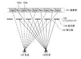
120 パララックスバリア
122 右目
123 左目
124 遮光部
125 開口部
130 レンチキュラーレンズ
140 マイクロレンズアレイ
400 液晶表示装置
401 画像メモリ
402 画像処理回路
403 コントローラ
404 液晶パネル
405 光供給部
406 光供給部制御回路
407 光学系
408 画素部
409 信号線駆動回路
410 走査線駆動回路
411 フルカラー画像データ
420 表示領域
421 表示領域
422 表示領域
450 シフトレジスタ
451 レベルシフタ
452 デジタルバッファ
453 記憶回路
454 記憶回路
455 アナログバッファ
460 シフトレジスタ
461 セレクタ
462 レベルシフタ
463 デジタルバッファ
500 基板
501 導電膜
502 導電膜
503 導電膜
504 導電膜
505 画素電極
506 ゲート絶縁膜
507 活性層
510 スペーサ
512 絶縁膜
513 絶縁膜
514 基板
515 対向電極
516 液晶層
517 遮蔽膜
520 半導体膜
521 導電膜
523 半導体膜
600 基板
601 導電膜
602 導電膜
603 導電膜
604 導電膜
605 画素電極
606 ゲート絶縁膜
607 活性層
608 共通電極
609 絶縁膜
610 スペーサ
612 絶縁膜
613 絶縁膜
614 基板
616 液晶層
104a 右目用画素
104b 左目用画素
105a 表示領域
105b 表示領域
105c 表示領域
1601 液晶パネル
1602 拡散板
1603 プリズムシート
1604 拡散板
1605 導光板
1607 バックライトパネル
1608 回路基板
1609 COFテープ
1610 FPC
1611 基板
1612 バックライト
1620 バックライト
1630 光学系
5001 筐体
5002 筐体
5003 表示部
5004 表示部
5005 マイクロホン
5006 スピーカー
5007 操作キー
5008 スタイラス
5201 筐体
5202 表示部
5203 キーボード
5204 ポインティングデバイス
5401 筐体
5402 表示部
5403 操作キー
Claims (8)
- 第1表示領域及び第2表示領域を有する画素部と、
互いに異なる色相を有する複数の光を順に前記第1表示領域に供給し、前記複数の光を順に前記第2表示領域に供給する光供給部と、
光学系と、
第1の走査線駆動回路と、第2の走査線駆動回路とを有し、
前記複数の光のうち、前記第1表示領域及び前記第2表示領域に並行して供給される2つの光の色相は、互いに異なり、
前記第1表示領域及び前記第2表示領域のそれぞれは、単数または複数行の画素を有し、
前記単数または複数行の画素は、右目に対応した画素と左目に対応した画素とを複数組有し、
前記複数の光を前記第1表示領域及び前記第2表示領域に供給することで、前記右目に対応した画素から第1の光が得られ、なおかつ、前記左目に対応した画素から第2の光が得られ、
前記光学系によって、前記第1の光の進行方向及び前記第2の光の進行方向は、互いに異なる向きにそれぞれ制御され、
前記第1の走査線駆動回路によって、前記第1の表示領域が有する走査線の電位が制御され、
前記第2の走査線駆動回路によって、前記第2の表示領域が有する走査線の電位が制御されることを特徴とする液晶表示装置。 - 第1表示領域及び第2表示領域を有する画素部と、
互いに異なる色相を有する複数の光を順に前記第1表示領域に供給し、前記複数の光を順に前記第2表示領域に供給する光供給部と、
光学系と、
第1の走査線駆動回路と、第2の走査線駆動回路とを有し、
前記複数の光のうち、前記第1表示領域及び前記第2表示領域に並行して供給される2つの光の色相は、互いに異なり、
前記第1表示領域及び前記第2表示領域のそれぞれは、単数または複数行の画素を有し、
前記単数または複数行の画素は、隣接した一対の画素を複数組有し、
前記複数の光を前記第1表示領域及び前記第2表示領域に供給することで、前記一対の画素の一方から第1の光が得られ、なおかつ、前記一対の画素の他方から第2の光が得られ、
前記光学系によって、前記第1の光の進行方向は観察者の右目に向けられるように、前記第2の光の進行方向は観察者の左目に向けられるように、それぞれ制御され、
前記第1の走査線駆動回路によって、前記第1の表示領域が有する走査線の電位が制御され、
前記第2の走査線駆動回路によって、前記第2の表示領域が有する走査線の電位が制御されることを特徴とする液晶表示装置。 - 請求項1または請求項2において、
第3の表示領域を有し、
前記第3の表示領域は、単数または複数行の画素を有し、
前記第1の表示領域が有する一の走査線が選択された直後に、前記第2の表示領域が有する一の走査線が選択され、
前記第2の表示領域が有する前記一の走査線が選択された直後に、前記第3の表示領域が有する一の走査線が選択されることを特徴とする液晶表示装置。 - 第1表示領域乃至第3表示領域を有する画素部と、
互いに異なる色相を有する複数の光を順に前記第1表示領域に供給し、前記複数の光を順に前記第2表示領域に供給する光供給部と、
光学系とを有し、
前記複数の光のうち、前記第1表示領域及び前記第2表示領域に並行して供給される2つの光の色相は、互いに異なり、
前記第1表示領域乃至前記第3表示領域のそれぞれは、単数または複数行の画素を有し、
前記単数または複数行の画素は、右目に対応した画素と左目に対応した画素とを複数組有し、
前記第1の表示領域が有する一の走査線が選択された直後に、前記第2の表示領域が有する一の走査線が選択され、
前記第2の表示領域が有する前記一の走査線が選択された直後に、前記第3の表示領域が有する一の走査線が選択され、
前記複数の光を前記第1表示領域及び前記第2表示領域に供給することで、前記右目に対応した画素から第1の光が得られ、なおかつ、前記左目に対応した画素から第2の光が得られ、
前記光学系によって、前記第1の光の進行方向及び前記第2の光の進行方向は、互いに異なる向きにそれぞれ制御されることを特徴とする液晶表示装置。 - 第1表示領域乃至第3表示領域を有する画素部と、
互いに異なる色相を有する複数の光を順に前記第1表示領域に供給し、前記複数の光を順に前記第2表示領域に供給する光供給部と、
光学系とを有し、
前記複数の光のうち、前記第1表示領域及び前記第2表示領域に並行して供給される2つの光の色相は、互いに異なり、
前記第1表示領域乃至前記第3表示領域のそれぞれは、単数または複数行の画素を有し、
前記単数または複数行の画素は、隣接した一対の画素を複数組有し、
前記第1の表示領域が有する一の走査線が選択された直後に、前記第2の表示領域が有する一の走査線が選択され、
前記第2の表示領域が有する前記一の走査線が選択された直後に、前記第3の表示領域が有する一の走査線が選択され、
前記複数の光を前記第1表示領域及び前記第2表示領域に供給することで、前記一対の画素の一方から第1の光が得られ、なおかつ、前記一対の画素の他方から第2の光が得られ、
前記光学系によって、前記第1の光の進行方向は観察者の右目に向けられるように、前記第2の光の進行方向は観察者の左目に向けられるように、それぞれ制御されることを特徴とする液晶表示装置。 - 請求項1乃至請求項5のいずれか一において、
前記画素は、トランジスタと、前記トランジスタを介して画像信号が与えられる液晶素子とを有し、
前記トランジスタは、活性層に酸化物半導体を含むことを特徴とする液晶表示装置。 - 請求項6において、
前記酸化物半導体は、In、Ga、Zn及びOを有することを特徴とする液晶表示装置。 - 請求項7において、前記酸化物半導体の水素濃度は、5×10¹⁹/cm3以下であることを特徴とする液晶表示装置。
Priority Applications (1)
| Application Number | Priority Date | Filing Date | Title |
|---|---|---|---|
| JP2011274245A JP6013677B2 (ja) | 2010-12-17 | 2011-12-15 | 液晶表示装置 |
Applications Claiming Priority (3)
| Application Number | Priority Date | Filing Date | Title |
|---|---|---|---|
| JP2010281177 | 2010-12-17 | ||
| JP2010281177 | 2010-12-17 | ||
| JP2011274245A JP6013677B2 (ja) | 2010-12-17 | 2011-12-15 | 液晶表示装置 |
Related Child Applications (1)
| Application Number | Title | Priority Date | Filing Date |
|---|---|---|---|
| JP2016184923A Division JP6313831B2 (ja) | 2010-12-17 | 2016-09-22 | 液晶表示装置 |
Publications (3)
| Publication Number | Publication Date |
|---|---|
| JP2012141602A JP2012141602A (ja) | 2012-07-26 |
| JP2012141602A5 JP2012141602A5 (ja) | 2015-02-05 |
| JP6013677B2 true JP6013677B2 (ja) | 2016-10-25 |
Family
ID=46233952
Family Applications (2)
| Application Number | Title | Priority Date | Filing Date |
|---|---|---|---|
| JP2011274245A Expired - Fee Related JP6013677B2 (ja) | 2010-12-17 | 2011-12-15 | 液晶表示装置 |
| JP2016184923A Active JP6313831B2 (ja) | 2010-12-17 | 2016-09-22 | 液晶表示装置 |
Family Applications After (1)
| Application Number | Title | Priority Date | Filing Date |
|---|---|---|---|
| JP2016184923A Active JP6313831B2 (ja) | 2010-12-17 | 2016-09-22 | 液晶表示装置 |
Country Status (3)
| Country | Link |
|---|---|
| US (1) | US8730416B2 (ja) |
| JP (2) | JP6013677B2 (ja) |
| KR (1) | KR20120068715A (ja) |
Families Citing this family (16)
| Publication number | Priority date | Publication date | Assignee | Title |
|---|---|---|---|---|
| US9167234B2 (en) | 2011-02-14 | 2015-10-20 | Semiconductor Energy Laboratory Co., Ltd. | Display device |
| US9035860B2 (en) | 2011-02-16 | 2015-05-19 | Semiconductor Energy Laboratory Co., Ltd. | Display device |
| US9443455B2 (en) | 2011-02-25 | 2016-09-13 | Semiconductor Energy Laboratory Co., Ltd. | Display device having a plurality of pixels |
| TW201250999A (en) * | 2011-06-13 | 2012-12-16 | Wintek Corp | Organic electroluminescent display device |
| US8988411B2 (en) | 2011-07-08 | 2015-03-24 | Semiconductor Energy Laboratory Co., Ltd. | Display device |
| KR101931331B1 (ko) * | 2012-01-09 | 2018-12-21 | 삼성디스플레이 주식회사 | 입체 영상 표시 장치 |
| JP2014032399A (ja) | 2012-07-13 | 2014-02-20 | Semiconductor Energy Lab Co Ltd | 液晶表示装置 |
| JP6098064B2 (ja) * | 2012-08-08 | 2017-03-22 | ソニー株式会社 | 表示装置および照明装置 |
| CN103578392B (zh) * | 2012-08-09 | 2016-07-27 | 瀚宇彩晶股份有限公司 | 裸眼式立体显示器及其驱动方法 |
| KR101501016B1 (ko) * | 2013-05-02 | 2015-03-10 | 주식회사 루멘스 | 3d 디스플레이 장치 |
| KR102069178B1 (ko) | 2013-08-07 | 2020-01-23 | 삼성디스플레이 주식회사 | 영상 표시 방법 및 이를 수행하기 위한 표시 장치 |
| JP6411025B2 (ja) * | 2013-12-27 | 2018-10-24 | 国立大学法人 筑波大学 | 時分割型パララックスバリア式裸眼立体映像表示装置 |
| CN104102043B (zh) * | 2014-07-08 | 2017-03-22 | 京东方科技集团股份有限公司 | 一种双视场显示器及其驱动方法 |
| CN104090417B (zh) | 2014-07-10 | 2016-11-23 | 京东方科技集团股份有限公司 | 一种显示装置及其驱动方法 |
| CN104320651A (zh) * | 2014-11-14 | 2015-01-28 | 深圳市华星光电技术有限公司 | 3d快门眼镜以及3d显示系统 |
| CN106226915B (zh) | 2016-08-03 | 2018-12-21 | 京东方科技集团股份有限公司 | 一种显示模组及显示装置 |
Family Cites Families (122)
| Publication number | Priority date | Publication date | Assignee | Title |
|---|---|---|---|---|
| US5302987A (en) * | 1991-05-15 | 1994-04-12 | Sharp Kabushiki Kaisha | Active matrix substrate including connecting electrode with extended portion |
| US5247194A (en) * | 1991-05-24 | 1993-09-21 | Samsung Electronics Co., Ltd. | Thin film transistor with an increased switching rate |
| JP3224829B2 (ja) * | 1991-08-15 | 2001-11-05 | 株式会社東芝 | 有機電界効果型素子 |
| WO1997006554A2 (en) | 1995-08-03 | 1997-02-20 | Philips Electronics N.V. | Semiconductor device provided with transparent switching element |
| JP3625598B2 (ja) | 1995-12-30 | 2005-03-02 | 三星電子株式会社 | 液晶表示装置の製造方法 |
| US6108029A (en) * | 1997-08-22 | 2000-08-22 | Lo; Allen Kwok Wah | Dual-mode 2D/3D display system |
| JP4170454B2 (ja) | 1998-07-24 | 2008-10-22 | Hoya株式会社 | 透明導電性酸化物薄膜を有する物品及びその製造方法 |
| EP0997868B1 (en) | 1998-10-30 | 2012-03-14 | Semiconductor Energy Laboratory Co., Ltd. | Field sequential liquid crystal display device and driving method thereof, and head mounted display |
| JP2000150861A (ja) | 1998-11-16 | 2000-05-30 | Tdk Corp | 酸化物薄膜 |
| JP3276930B2 (ja) | 1998-11-17 | 2002-04-22 | 科学技術振興事業団 | トランジスタ及び半導体装置 |
| US6597348B1 (en) | 1998-12-28 | 2003-07-22 | Semiconductor Energy Laboratory Co., Ltd. | Information-processing device |
| US7145536B1 (en) | 1999-03-26 | 2006-12-05 | Semiconductor Energy Laboratory Co., Ltd. | Liquid crystal display device |
| TW460731B (en) | 1999-09-03 | 2001-10-21 | Ind Tech Res Inst | Electrode structure and production method of wide viewing angle LCD |
| JP2001154205A (ja) * | 1999-11-24 | 2001-06-08 | Toshiba Corp | アクティブマトリクス型の液晶表示装置 |
| US6882012B2 (en) | 2000-02-28 | 2005-04-19 | Semiconductor Energy Laboratory Co., Ltd. | Semiconductor device and a method of manufacturing the same |
| TW518552B (en) | 2000-08-18 | 2003-01-21 | Semiconductor Energy Lab | Liquid crystal display device, method of driving the same, and method of driving a portable information device having the liquid crystal display device |
| JP4089858B2 (ja) | 2000-09-01 | 2008-05-28 | 国立大学法人東北大学 | 半導体デバイス |
| US7385579B2 (en) | 2000-09-29 | 2008-06-10 | Semiconductor Energy Laboratory Co., Ltd. | Liquid crystal display device and method of driving the same |
| KR20020038482A (ko) | 2000-11-15 | 2002-05-23 | 모리시타 요이찌 | 박막 트랜지스터 어레이, 그 제조방법 및 그것을 이용한표시패널 |
| JP3997731B2 (ja) | 2001-03-19 | 2007-10-24 | 富士ゼロックス株式会社 | 基材上に結晶性半導体薄膜を形成する方法 |
| JP2002289859A (ja) | 2001-03-23 | 2002-10-04 | Minolta Co Ltd | 薄膜トランジスタ |
| JP3925839B2 (ja) | 2001-09-10 | 2007-06-06 | シャープ株式会社 | 半導体記憶装置およびその試験方法 |
| JP4090716B2 (ja) | 2001-09-10 | 2008-05-28 | 雅司 川崎 | 薄膜トランジスタおよびマトリクス表示装置 |
| JP4164562B2 (ja) | 2002-09-11 | 2008-10-15 | 独立行政法人科学技術振興機構 | ホモロガス薄膜を活性層として用いる透明薄膜電界効果型トランジスタ |
| US7061014B2 (en) | 2001-11-05 | 2006-06-13 | Japan Science And Technology Agency | Natural-superlattice homologous single crystal thin film, method for preparation thereof, and device using said single crystal thin film |
| JP4083486B2 (ja) | 2002-02-21 | 2008-04-30 | 独立行政法人科学技術振興機構 | LnCuO(S,Se,Te)単結晶薄膜の製造方法 |
| JP2003259395A (ja) | 2002-03-06 | 2003-09-12 | Matsushita Electric Ind Co Ltd | 立体表示方法及び立体表示装置 |
| US7049190B2 (en) | 2002-03-15 | 2006-05-23 | Sanyo Electric Co., Ltd. | Method for forming ZnO film, method for forming ZnO semiconductor layer, method for fabricating semiconductor device, and semiconductor device |
| JP3933591B2 (ja) | 2002-03-26 | 2007-06-20 | 淳二 城戸 | 有機エレクトロルミネッセント素子 |
| US7339187B2 (en) | 2002-05-21 | 2008-03-04 | State Of Oregon Acting By And Through The Oregon State Board Of Higher Education On Behalf Of Oregon State University | Transistor structures |
| JP2004022625A (ja) | 2002-06-13 | 2004-01-22 | Murata Mfg Co Ltd | 半導体デバイス及び該半導体デバイスの製造方法 |
| US7105868B2 (en) | 2002-06-24 | 2006-09-12 | Cermet, Inc. | High-electron mobility transistor with zinc oxide |
| JP2004077567A (ja) | 2002-08-09 | 2004-03-11 | Semiconductor Energy Lab Co Ltd | 表示装置及びその駆動方法 |
| JP2004094058A (ja) | 2002-09-02 | 2004-03-25 | Semiconductor Energy Lab Co Ltd | 液晶表示装置および液晶表示装置の駆動方法 |
| US7193593B2 (en) | 2002-09-02 | 2007-03-20 | Semiconductor Energy Laboratory Co., Ltd. | Liquid crystal display device and method of driving a liquid crystal display device |
| US7067843B2 (en) | 2002-10-11 | 2006-06-27 | E. I. Du Pont De Nemours And Company | Transparent oxide semiconductor thin film transistors |
| JP4166105B2 (ja) | 2003-03-06 | 2008-10-15 | シャープ株式会社 | 半導体装置およびその製造方法 |
| JP2004273732A (ja) | 2003-03-07 | 2004-09-30 | Sharp Corp | アクティブマトリクス基板およびその製造方法 |
| JP4108633B2 (ja) | 2003-06-20 | 2008-06-25 | シャープ株式会社 | 薄膜トランジスタおよびその製造方法ならびに電子デバイス |
| TWI399580B (zh) | 2003-07-14 | 2013-06-21 | Semiconductor Energy Lab | 半導體裝置及顯示裝置 |
| US7262463B2 (en) | 2003-07-25 | 2007-08-28 | Hewlett-Packard Development Company, L.P. | Transistor including a deposited channel region having a doped portion |
| CN102867855B (zh) | 2004-03-12 | 2015-07-15 | 独立行政法人科学技术振兴机构 | 薄膜晶体管及其制造方法 |
| US7145174B2 (en) | 2004-03-12 | 2006-12-05 | Hewlett-Packard Development Company, Lp. | Semiconductor device |
| US7282782B2 (en) | 2004-03-12 | 2007-10-16 | Hewlett-Packard Development Company, L.P. | Combined binary oxide semiconductor device |
| US7297977B2 (en) | 2004-03-12 | 2007-11-20 | Hewlett-Packard Development Company, L.P. | Semiconductor device |
| CN100557667C (zh) | 2004-04-22 | 2009-11-04 | 株式会社半导体能源研究所 | 发光装置及其驱动方法 |
| US7211825B2 (en) | 2004-06-14 | 2007-05-01 | Yi-Chi Shih | Indium oxide-based thin film transistors and circuits |
| JP2006100760A (ja) | 2004-09-02 | 2006-04-13 | Casio Comput Co Ltd | 薄膜トランジスタおよびその製造方法 |
| KR100637530B1 (ko) * | 2004-09-08 | 2006-10-23 | 삼성에스디아이 주식회사 | 2d/3d 겸용 영상 표시 장치 및 액정 표시 패널 |
| US7285501B2 (en) | 2004-09-17 | 2007-10-23 | Hewlett-Packard Development Company, L.P. | Method of forming a solution processed device |
| US7298084B2 (en) | 2004-11-02 | 2007-11-20 | 3M Innovative Properties Company | Methods and displays utilizing integrated zinc oxide row and column drivers in conjunction with organic light emitting diodes |
| WO2006051994A2 (en) | 2004-11-10 | 2006-05-18 | Canon Kabushiki Kaisha | Light-emitting device |
| US7829444B2 (en) | 2004-11-10 | 2010-11-09 | Canon Kabushiki Kaisha | Field effect transistor manufacturing method |
| CA2585071A1 (en) | 2004-11-10 | 2006-05-18 | Canon Kabushiki Kaisha | Field effect transistor employing an amorphous oxide |
| US7863611B2 (en) | 2004-11-10 | 2011-01-04 | Canon Kabushiki Kaisha | Integrated circuits utilizing amorphous oxides |
| CN102945857B (zh) | 2004-11-10 | 2015-06-03 | 佳能株式会社 | 无定形氧化物和场效应晶体管 |
| US7791072B2 (en) | 2004-11-10 | 2010-09-07 | Canon Kabushiki Kaisha | Display |
| US7453065B2 (en) | 2004-11-10 | 2008-11-18 | Canon Kabushiki Kaisha | Sensor and image pickup device |
| US7675582B2 (en) * | 2004-12-03 | 2010-03-09 | Au Optronics Corporation | Stacked storage capacitor structure for a thin film transistor liquid crystal display |
| US7579224B2 (en) | 2005-01-21 | 2009-08-25 | Semiconductor Energy Laboratory Co., Ltd. | Method for manufacturing a thin film semiconductor device |
| TWI390735B (zh) | 2005-01-28 | 2013-03-21 | Semiconductor Energy Lab | 半導體裝置,電子裝置,和半導體裝置的製造方法 |
| TWI412138B (zh) | 2005-01-28 | 2013-10-11 | Semiconductor Energy Lab | 半導體裝置,電子裝置,和半導體裝置的製造方法 |
| US7858451B2 (en) | 2005-02-03 | 2010-12-28 | Semiconductor Energy Laboratory Co., Ltd. | Electronic device, semiconductor device and manufacturing method thereof |
| JP4138759B2 (ja) * | 2005-02-03 | 2008-08-27 | セイコーエプソン株式会社 | 液晶表示装置および電子機器 |
| US7948171B2 (en) | 2005-02-18 | 2011-05-24 | Semiconductor Energy Laboratory Co., Ltd. | Light emitting device |
| US20060197092A1 (en) | 2005-03-03 | 2006-09-07 | Randy Hoffman | System and method for forming conductive material on a substrate |
| US8681077B2 (en) | 2005-03-18 | 2014-03-25 | Semiconductor Energy Laboratory Co., Ltd. | Semiconductor device, and display device, driving method and electronic apparatus thereof |
| US7544967B2 (en) | 2005-03-28 | 2009-06-09 | Massachusetts Institute Of Technology | Low voltage flexible organic/transparent transistor for selective gas sensing, photodetecting and CMOS device applications |
| US7645478B2 (en) | 2005-03-31 | 2010-01-12 | 3M Innovative Properties Company | Methods of making displays |
| US8300031B2 (en) | 2005-04-20 | 2012-10-30 | Semiconductor Energy Laboratory Co., Ltd. | Semiconductor device comprising transistor having gate and drain connected through a current-voltage conversion element |
| JP2006344849A (ja) | 2005-06-10 | 2006-12-21 | Casio Comput Co Ltd | 薄膜トランジスタ |
| US7402506B2 (en) | 2005-06-16 | 2008-07-22 | Eastman Kodak Company | Methods of making thin film transistors comprising zinc-oxide-based semiconductor materials and transistors made thereby |
| US7691666B2 (en) | 2005-06-16 | 2010-04-06 | Eastman Kodak Company | Methods of making thin film transistors comprising zinc-oxide-based semiconductor materials and transistors made thereby |
| US7507618B2 (en) | 2005-06-27 | 2009-03-24 | 3M Innovative Properties Company | Method for making electronic devices using metal oxide nanoparticles |
| KR100711890B1 (ko) | 2005-07-28 | 2007-04-25 | 삼성에스디아이 주식회사 | 유기 발광표시장치 및 그의 제조방법 |
| JP2007059128A (ja) | 2005-08-23 | 2007-03-08 | Canon Inc | 有機el表示装置およびその製造方法 |
| JP4280736B2 (ja) | 2005-09-06 | 2009-06-17 | キヤノン株式会社 | 半導体素子 |
| JP4850457B2 (ja) | 2005-09-06 | 2012-01-11 | キヤノン株式会社 | 薄膜トランジスタ及び薄膜ダイオード |
| JP5116225B2 (ja) | 2005-09-06 | 2013-01-09 | キヤノン株式会社 | 酸化物半導体デバイスの製造方法 |
| JP4560502B2 (ja) * | 2005-09-06 | 2010-10-13 | キヤノン株式会社 | 電界効果型トランジスタ |
| JP2007073705A (ja) | 2005-09-06 | 2007-03-22 | Canon Inc | 酸化物半導体チャネル薄膜トランジスタおよびその製造方法 |
| EP3614442A3 (en) | 2005-09-29 | 2020-03-25 | Semiconductor Energy Laboratory Co., Ltd. | Semiconductor device having oxide semiconductor layer and manufactoring method thereof |
| JP5037808B2 (ja) | 2005-10-20 | 2012-10-03 | キヤノン株式会社 | アモルファス酸化物を用いた電界効果型トランジスタ、及び該トランジスタを用いた表示装置 |
| WO2007058329A1 (en) | 2005-11-15 | 2007-05-24 | Semiconductor Energy Laboratory Co., Ltd. | Semiconductor device and manufacturing method thereof |
| TWI292281B (en) | 2005-12-29 | 2008-01-01 | Ind Tech Res Inst | Pixel structure of active organic light emitting diode and method of fabricating the same |
| US7867636B2 (en) | 2006-01-11 | 2011-01-11 | Murata Manufacturing Co., Ltd. | Transparent conductive film and method for manufacturing the same |
| JP4977478B2 (ja) | 2006-01-21 | 2012-07-18 | 三星電子株式会社 | ZnOフィルム及びこれを用いたTFTの製造方法 |
| US7576394B2 (en) | 2006-02-02 | 2009-08-18 | Kochi Industrial Promotion Center | Thin film transistor including low resistance conductive thin films and manufacturing method thereof |
| US7977169B2 (en) | 2006-02-15 | 2011-07-12 | Kochi Industrial Promotion Center | Semiconductor device including active layer made of zinc oxide with controlled orientations and manufacturing method thereof |
| KR20070101595A (ko) | 2006-04-11 | 2007-10-17 | 삼성전자주식회사 | ZnO TFT |
| US20070252928A1 (en) | 2006-04-28 | 2007-11-01 | Toppan Printing Co., Ltd. | Structure, transmission type liquid crystal display, reflection type display and manufacturing method thereof |
| US8106865B2 (en) | 2006-06-02 | 2012-01-31 | Semiconductor Energy Laboratory Co., Ltd. | Display device and driving method thereof |
| US8154493B2 (en) | 2006-06-02 | 2012-04-10 | Semiconductor Energy Laboratory Co., Ltd. | Liquid crystal display device, driving method of the same, and electronic device using the same |
| JP5028033B2 (ja) | 2006-06-13 | 2012-09-19 | キヤノン株式会社 | 酸化物半導体膜のドライエッチング方法 |
| JP4609797B2 (ja) | 2006-08-09 | 2011-01-12 | Nec液晶テクノロジー株式会社 | 薄膜デバイス及びその製造方法 |
| JP4999400B2 (ja) | 2006-08-09 | 2012-08-15 | キヤノン株式会社 | 酸化物半導体膜のドライエッチング方法 |
| JP4332545B2 (ja) | 2006-09-15 | 2009-09-16 | キヤノン株式会社 | 電界効果型トランジスタ及びその製造方法 |
| JP5164357B2 (ja) | 2006-09-27 | 2013-03-21 | キヤノン株式会社 | 半導体装置及び半導体装置の製造方法 |
| JP4274219B2 (ja) | 2006-09-27 | 2009-06-03 | セイコーエプソン株式会社 | 電子デバイス、有機エレクトロルミネッセンス装置、有機薄膜半導体装置 |
| US7622371B2 (en) | 2006-10-10 | 2009-11-24 | Hewlett-Packard Development Company, L.P. | Fused nanocrystal thin film semiconductor and method |
| US7772021B2 (en) | 2006-11-29 | 2010-08-10 | Samsung Electronics Co., Ltd. | Flat panel displays comprising a thin-film transistor having a semiconductive oxide in its channel and methods of fabricating the same for use in flat panel displays |
| JP2008140684A (ja) | 2006-12-04 | 2008-06-19 | Toppan Printing Co Ltd | カラーelディスプレイおよびその製造方法 |
| KR101303578B1 (ko) | 2007-01-05 | 2013-09-09 | 삼성전자주식회사 | 박막 식각 방법 |
| US8207063B2 (en) | 2007-01-26 | 2012-06-26 | Eastman Kodak Company | Process for atomic layer deposition |
| KR100851215B1 (ko) | 2007-03-14 | 2008-08-07 | 삼성에스디아이 주식회사 | 박막 트랜지스터 및 이를 이용한 유기 전계 발광표시장치 |
| US7795613B2 (en) | 2007-04-17 | 2010-09-14 | Toppan Printing Co., Ltd. | Structure with transistor |
| KR101325053B1 (ko) | 2007-04-18 | 2013-11-05 | 삼성디스플레이 주식회사 | 박막 트랜지스터 기판 및 이의 제조 방법 |
| KR20080094300A (ko) | 2007-04-19 | 2008-10-23 | 삼성전자주식회사 | 박막 트랜지스터 및 그 제조 방법과 박막 트랜지스터를포함하는 평판 디스플레이 |
| KR101334181B1 (ko) | 2007-04-20 | 2013-11-28 | 삼성전자주식회사 | 선택적으로 결정화된 채널층을 갖는 박막 트랜지스터 및 그제조 방법 |
| WO2008133345A1 (en) | 2007-04-25 | 2008-11-06 | Canon Kabushiki Kaisha | Oxynitride semiconductor |
| KR101345376B1 (ko) | 2007-05-29 | 2013-12-24 | 삼성전자주식회사 | ZnO 계 박막 트랜지스터 및 그 제조방법 |
| JP5215158B2 (ja) | 2007-12-17 | 2013-06-19 | 富士フイルム株式会社 | 無機結晶性配向膜及びその製造方法、半導体デバイス |
| US9041202B2 (en) * | 2008-05-16 | 2015-05-26 | Semiconductor Energy Laboratory Co., Ltd. | Semiconductor device and manufacturing method of the same |
| KR101703511B1 (ko) | 2008-06-27 | 2017-02-07 | 가부시키가이샤 한도오따이 에네루기 켄큐쇼 | 박막 트랜지스터 |
| JP4623179B2 (ja) | 2008-09-18 | 2011-02-02 | ソニー株式会社 | 薄膜トランジスタおよびその製造方法 |
| JP5451280B2 (ja) | 2008-10-09 | 2014-03-26 | キヤノン株式会社 | ウルツ鉱型結晶成長用基板およびその製造方法ならびに半導体装置 |
| JP5590868B2 (ja) | 2008-12-11 | 2014-09-17 | 株式会社半導体エネルギー研究所 | 半導体装置 |
| KR101719350B1 (ko) * | 2008-12-25 | 2017-03-23 | 가부시키가이샤 한도오따이 에네루기 켄큐쇼 | 반도체 장치 및 그 제작 방법 |
| JP5100670B2 (ja) | 2009-01-21 | 2012-12-19 | 株式会社半導体エネルギー研究所 | タッチパネル、電子機器 |
| US8461582B2 (en) * | 2009-03-05 | 2013-06-11 | Semiconductor Energy Laboratory Co., Ltd. | Semiconductor device and method for manufacturing the same |
| KR101759585B1 (ko) * | 2009-03-17 | 2017-07-19 | 코닌클리케 필립스 엔.브이. | 컬러 순차적 디스플레이들을 구동하는 방법들 |
| US8427591B2 (en) * | 2010-03-17 | 2013-04-23 | 3Dv Co. Ltd. | 3D liquid crystal display system |
-
2011
- 2011-12-01 US US13/308,601 patent/US8730416B2/en not_active Expired - Fee Related
- 2011-12-15 KR KR1020110135123A patent/KR20120068715A/ko not_active Application Discontinuation
- 2011-12-15 JP JP2011274245A patent/JP6013677B2/ja not_active Expired - Fee Related
-
2016
- 2016-09-22 JP JP2016184923A patent/JP6313831B2/ja active Active
Also Published As
| Publication number | Publication date |
|---|---|
| JP2012141602A (ja) | 2012-07-26 |
| JP2017033006A (ja) | 2017-02-09 |
| JP6313831B2 (ja) | 2018-04-18 |
| US20120154696A1 (en) | 2012-06-21 |
| KR20120068715A (ko) | 2012-06-27 |
| US8730416B2 (en) | 2014-05-20 |
Similar Documents
| Publication | Publication Date | Title |
|---|---|---|
| JP6313831B2 (ja) | 液晶表示装置 | |
| JP6914311B2 (ja) | 液晶表示装置 | |
| US20170140719A1 (en) | Liquid crystal display device and driving method thereof | |
| JP2023162301A (ja) | 液晶表示装置 | |
| JP6487503B2 (ja) | 液晶表示装置 | |
| TWI549474B (zh) | 顯示裝置 | |
| JP6750077B2 (ja) | 表示装置 | |
| TW201104871A (en) | Semiconductor device and method for manufacturing the same | |
| CN102714023A (zh) | 液晶显示设备的驱动方法 | |
| JP2021107923A (ja) | 半導体装置 | |
| JP2012129988A (ja) | 立体映像表示装置の駆動方法 | |
| JP5832204B2 (ja) | 表示システム | |
| JP5832872B2 (ja) | 液晶表示装置の駆動方法 | |
| US20130235093A1 (en) | Method for driving display device, display device, and electronic device | |
| KR20120056210A (ko) | 입체 영상 표시 장치의 구동 방법 |
Legal Events
| Date | Code | Title | Description |
|---|---|---|---|
| A521 | Request for written amendment filed |
Free format text: JAPANESE INTERMEDIATE CODE: A523 Effective date: 20141212 |
|
| A621 | Written request for application examination |
Free format text: JAPANESE INTERMEDIATE CODE: A621 Effective date: 20141212 |
|
| A977 | Report on retrieval |
Free format text: JAPANESE INTERMEDIATE CODE: A971007 Effective date: 20150817 |
|
| A131 | Notification of reasons for refusal |
Free format text: JAPANESE INTERMEDIATE CODE: A131 Effective date: 20150901 |
|
| A521 | Request for written amendment filed |
Free format text: JAPANESE INTERMEDIATE CODE: A523 Effective date: 20151007 |
|
| A131 | Notification of reasons for refusal |
Free format text: JAPANESE INTERMEDIATE CODE: A131 Effective date: 20160329 |
|
| A521 | Request for written amendment filed |
Free format text: JAPANESE INTERMEDIATE CODE: A523 Effective date: 20160418 |
|
| TRDD | Decision of grant or rejection written | ||
| A01 | Written decision to grant a patent or to grant a registration (utility model) |
Free format text: JAPANESE INTERMEDIATE CODE: A01 Effective date: 20160906 |
|
| A61 | First payment of annual fees (during grant procedure) |
Free format text: JAPANESE INTERMEDIATE CODE: A61 Effective date: 20160922 |
|
| R150 | Certificate of patent or registration of utility model |
Ref document number: 6013677 Country of ref document: JP Free format text: JAPANESE INTERMEDIATE CODE: R150 |
|
| R250 | Receipt of annual fees |
Free format text: JAPANESE INTERMEDIATE CODE: R250 |
|
| LAPS | Cancellation because of no payment of annual fees |