JP6013677B2 - Liquid crystal display - Google Patents
Liquid crystal display Download PDFInfo
- Publication number
- JP6013677B2 JP6013677B2 JP2011274245A JP2011274245A JP6013677B2 JP 6013677 B2 JP6013677 B2 JP 6013677B2 JP 2011274245 A JP2011274245 A JP 2011274245A JP 2011274245 A JP2011274245 A JP 2011274245A JP 6013677 B2 JP6013677 B2 JP 6013677B2
- Authority
- JP
- Japan
- Prior art keywords
- display area
- light
- liquid crystal
- pixel
- pixels
- Prior art date
- Legal status (The legal status is an assumption and is not a legal conclusion. Google has not performed a legal analysis and makes no representation as to the accuracy of the status listed.)
- Expired - Fee Related
Links
Images


Classifications
-
- G—PHYSICS
- G09—EDUCATION; CRYPTOGRAPHY; DISPLAY; ADVERTISING; SEALS
- G09G—ARRANGEMENTS OR CIRCUITS FOR CONTROL OF INDICATING DEVICES USING STATIC MEANS TO PRESENT VARIABLE INFORMATION
- G09G3/00—Control arrangements or circuits, of interest only in connection with visual indicators other than cathode-ray tubes
- G09G3/001—Control arrangements or circuits, of interest only in connection with visual indicators other than cathode-ray tubes using specific devices not provided for in groups G09G3/02 - G09G3/36, e.g. using an intermediate record carrier such as a film slide; Projection systems; Display of non-alphanumerical information, solely or in combination with alphanumerical information, e.g. digital display on projected diapositive as background
- G09G3/003—Control arrangements or circuits, of interest only in connection with visual indicators other than cathode-ray tubes using specific devices not provided for in groups G09G3/02 - G09G3/36, e.g. using an intermediate record carrier such as a film slide; Projection systems; Display of non-alphanumerical information, solely or in combination with alphanumerical information, e.g. digital display on projected diapositive as background to produce spatial visual effects
-
- G—PHYSICS
- G02—OPTICS
- G02B—OPTICAL ELEMENTS, SYSTEMS OR APPARATUS
- G02B30/00—Optical systems or apparatus for producing three-dimensional [3D] effects, e.g. stereoscopic images
- G02B30/20—Optical systems or apparatus for producing three-dimensional [3D] effects, e.g. stereoscopic images by providing first and second parallax images to an observer's left and right eyes
- G02B30/26—Optical systems or apparatus for producing three-dimensional [3D] effects, e.g. stereoscopic images by providing first and second parallax images to an observer's left and right eyes of the autostereoscopic type
- G02B30/27—Optical systems or apparatus for producing three-dimensional [3D] effects, e.g. stereoscopic images by providing first and second parallax images to an observer's left and right eyes of the autostereoscopic type involving lenticular arrays
-
- G—PHYSICS
- G02—OPTICS
- G02B—OPTICAL ELEMENTS, SYSTEMS OR APPARATUS
- G02B30/00—Optical systems or apparatus for producing three-dimensional [3D] effects, e.g. stereoscopic images
- G02B30/20—Optical systems or apparatus for producing three-dimensional [3D] effects, e.g. stereoscopic images by providing first and second parallax images to an observer's left and right eyes
- G02B30/26—Optical systems or apparatus for producing three-dimensional [3D] effects, e.g. stereoscopic images by providing first and second parallax images to an observer's left and right eyes of the autostereoscopic type
- G02B30/30—Optical systems or apparatus for producing three-dimensional [3D] effects, e.g. stereoscopic images by providing first and second parallax images to an observer's left and right eyes of the autostereoscopic type involving parallax barriers
-
- G—PHYSICS
- G02—OPTICS
- G02F—OPTICAL DEVICES OR ARRANGEMENTS FOR THE CONTROL OF LIGHT BY MODIFICATION OF THE OPTICAL PROPERTIES OF THE MEDIA OF THE ELEMENTS INVOLVED THEREIN; NON-LINEAR OPTICS; FREQUENCY-CHANGING OF LIGHT; OPTICAL LOGIC ELEMENTS; OPTICAL ANALOGUE/DIGITAL CONVERTERS
- G02F1/00—Devices or arrangements for the control of the intensity, colour, phase, polarisation or direction of light arriving from an independent light source, e.g. switching, gating or modulating; Non-linear optics
- G02F1/01—Devices or arrangements for the control of the intensity, colour, phase, polarisation or direction of light arriving from an independent light source, e.g. switching, gating or modulating; Non-linear optics for the control of the intensity, phase, polarisation or colour
- G02F1/13—Devices or arrangements for the control of the intensity, colour, phase, polarisation or direction of light arriving from an independent light source, e.g. switching, gating or modulating; Non-linear optics for the control of the intensity, phase, polarisation or colour based on liquid crystals, e.g. single liquid crystal display cells
- G02F1/1323—Arrangements for providing a switchable viewing angle
-
- G—PHYSICS
- G02—OPTICS
- G02F—OPTICAL DEVICES OR ARRANGEMENTS FOR THE CONTROL OF LIGHT BY MODIFICATION OF THE OPTICAL PROPERTIES OF THE MEDIA OF THE ELEMENTS INVOLVED THEREIN; NON-LINEAR OPTICS; FREQUENCY-CHANGING OF LIGHT; OPTICAL LOGIC ELEMENTS; OPTICAL ANALOGUE/DIGITAL CONVERTERS
- G02F1/00—Devices or arrangements for the control of the intensity, colour, phase, polarisation or direction of light arriving from an independent light source, e.g. switching, gating or modulating; Non-linear optics
- G02F1/01—Devices or arrangements for the control of the intensity, colour, phase, polarisation or direction of light arriving from an independent light source, e.g. switching, gating or modulating; Non-linear optics for the control of the intensity, phase, polarisation or colour
- G02F1/13—Devices or arrangements for the control of the intensity, colour, phase, polarisation or direction of light arriving from an independent light source, e.g. switching, gating or modulating; Non-linear optics for the control of the intensity, phase, polarisation or colour based on liquid crystals, e.g. single liquid crystal display cells
- G02F1/133—Constructional arrangements; Operation of liquid crystal cells; Circuit arrangements
- G02F1/1333—Constructional arrangements; Manufacturing methods
- G02F1/1335—Structural association of cells with optical devices, e.g. polarisers or reflectors
- G02F1/1336—Illuminating devices
- G02F1/133621—Illuminating devices providing coloured light
-
- G—PHYSICS
- G09—EDUCATION; CRYPTOGRAPHY; DISPLAY; ADVERTISING; SEALS
- G09G—ARRANGEMENTS OR CIRCUITS FOR CONTROL OF INDICATING DEVICES USING STATIC MEANS TO PRESENT VARIABLE INFORMATION
- G09G3/00—Control arrangements or circuits, of interest only in connection with visual indicators other than cathode-ray tubes
- G09G3/20—Control arrangements or circuits, of interest only in connection with visual indicators other than cathode-ray tubes for presentation of an assembly of a number of characters, e.g. a page, by composing the assembly by combination of individual elements arranged in a matrix no fixed position being assigned to or needed to be assigned to the individual characters or partial characters
- G09G3/34—Control arrangements or circuits, of interest only in connection with visual indicators other than cathode-ray tubes for presentation of an assembly of a number of characters, e.g. a page, by composing the assembly by combination of individual elements arranged in a matrix no fixed position being assigned to or needed to be assigned to the individual characters or partial characters by control of light from an independent source
- G09G3/36—Control arrangements or circuits, of interest only in connection with visual indicators other than cathode-ray tubes for presentation of an assembly of a number of characters, e.g. a page, by composing the assembly by combination of individual elements arranged in a matrix no fixed position being assigned to or needed to be assigned to the individual characters or partial characters by control of light from an independent source using liquid crystals
- G09G3/3611—Control of matrices with row and column drivers
- G09G3/3648—Control of matrices with row and column drivers using an active matrix
-
- H—ELECTRICITY
- H04—ELECTRIC COMMUNICATION TECHNIQUE
- H04N—PICTORIAL COMMUNICATION, e.g. TELEVISION
- H04N13/00—Stereoscopic video systems; Multi-view video systems; Details thereof
- H04N13/30—Image reproducers
- H04N13/302—Image reproducers for viewing without the aid of special glasses, i.e. using autostereoscopic displays
-
- H—ELECTRICITY
- H04—ELECTRIC COMMUNICATION TECHNIQUE
- H04N—PICTORIAL COMMUNICATION, e.g. TELEVISION
- H04N13/00—Stereoscopic video systems; Multi-view video systems; Details thereof
- H04N13/30—Image reproducers
- H04N13/324—Colour aspects
-
- G—PHYSICS
- G02—OPTICS
- G02F—OPTICAL DEVICES OR ARRANGEMENTS FOR THE CONTROL OF LIGHT BY MODIFICATION OF THE OPTICAL PROPERTIES OF THE MEDIA OF THE ELEMENTS INVOLVED THEREIN; NON-LINEAR OPTICS; FREQUENCY-CHANGING OF LIGHT; OPTICAL LOGIC ELEMENTS; OPTICAL ANALOGUE/DIGITAL CONVERTERS
- G02F1/00—Devices or arrangements for the control of the intensity, colour, phase, polarisation or direction of light arriving from an independent light source, e.g. switching, gating or modulating; Non-linear optics
- G02F1/01—Devices or arrangements for the control of the intensity, colour, phase, polarisation or direction of light arriving from an independent light source, e.g. switching, gating or modulating; Non-linear optics for the control of the intensity, phase, polarisation or colour
- G02F1/13—Devices or arrangements for the control of the intensity, colour, phase, polarisation or direction of light arriving from an independent light source, e.g. switching, gating or modulating; Non-linear optics for the control of the intensity, phase, polarisation or colour based on liquid crystals, e.g. single liquid crystal display cells
- G02F1/133—Constructional arrangements; Operation of liquid crystal cells; Circuit arrangements
- G02F1/1333—Constructional arrangements; Manufacturing methods
- G02F1/1335—Structural association of cells with optical devices, e.g. polarisers or reflectors
- G02F1/1336—Illuminating devices
- G02F1/133621—Illuminating devices providing coloured light
- G02F1/133622—Colour sequential illumination
-
- G—PHYSICS
- G02—OPTICS
- G02F—OPTICAL DEVICES OR ARRANGEMENTS FOR THE CONTROL OF LIGHT BY MODIFICATION OF THE OPTICAL PROPERTIES OF THE MEDIA OF THE ELEMENTS INVOLVED THEREIN; NON-LINEAR OPTICS; FREQUENCY-CHANGING OF LIGHT; OPTICAL LOGIC ELEMENTS; OPTICAL ANALOGUE/DIGITAL CONVERTERS
- G02F1/00—Devices or arrangements for the control of the intensity, colour, phase, polarisation or direction of light arriving from an independent light source, e.g. switching, gating or modulating; Non-linear optics
- G02F1/01—Devices or arrangements for the control of the intensity, colour, phase, polarisation or direction of light arriving from an independent light source, e.g. switching, gating or modulating; Non-linear optics for the control of the intensity, phase, polarisation or colour
- G02F1/13—Devices or arrangements for the control of the intensity, colour, phase, polarisation or direction of light arriving from an independent light source, e.g. switching, gating or modulating; Non-linear optics for the control of the intensity, phase, polarisation or colour based on liquid crystals, e.g. single liquid crystal display cells
- G02F1/137—Devices or arrangements for the control of the intensity, colour, phase, polarisation or direction of light arriving from an independent light source, e.g. switching, gating or modulating; Non-linear optics for the control of the intensity, phase, polarisation or colour based on liquid crystals, e.g. single liquid crystal display cells characterised by the electro-optical or magneto-optical effect, e.g. field-induced phase transition, orientation effect, guest-host interaction or dynamic scattering
- G02F1/13793—Blue phases
-
- G—PHYSICS
- G09—EDUCATION; CRYPTOGRAPHY; DISPLAY; ADVERTISING; SEALS
- G09G—ARRANGEMENTS OR CIRCUITS FOR CONTROL OF INDICATING DEVICES USING STATIC MEANS TO PRESENT VARIABLE INFORMATION
- G09G2310/00—Command of the display device
- G09G2310/02—Addressing, scanning or driving the display screen or processing steps related thereto
- G09G2310/0224—Details of interlacing
-
- G—PHYSICS
- G09—EDUCATION; CRYPTOGRAPHY; DISPLAY; ADVERTISING; SEALS
- G09G—ARRANGEMENTS OR CIRCUITS FOR CONTROL OF INDICATING DEVICES USING STATIC MEANS TO PRESENT VARIABLE INFORMATION
- G09G2310/00—Command of the display device
- G09G2310/02—Addressing, scanning or driving the display screen or processing steps related thereto
- G09G2310/0235—Field-sequential colour display
Description
三次元画像の表示を行う液晶表示装置に関する。 The present invention relates to a liquid crystal display device that displays a three-dimensional image.
三次元画像に対応した表示装置の市場が拡大傾向にある。三次元画像の表示は、両眼で立体の対象物を見たときに生ずるであろう、両眼間の網膜像の差異(両眼視差)を表示装置において作為的に作り出すことで、行うことができる。上記両眼視差を利用した三次元画像用の表示装置は、各種の表示方式が開発され商品化されているが、携帯情報端末や携帯型ゲーム機などの小型の表示装置では、パララックスバリア、レンチキュラーレンズ、マイクロレンズアレイなどの光学系を利用した直視タイプの表示方式が、主に採用されている。 The market for display devices that support 3D images is on the rise. 3D image display is performed by creating a difference in the retinal image (binocular parallax) between the eyes, which would occur when viewing a stereoscopic object with both eyes, on the display device. Can do. Various display methods have been developed and commercialized for the above three-dimensional image display devices using binocular parallax, but in small display devices such as portable information terminals and portable game machines, parallax barriers, A direct-view type display method using an optical system such as a lenticular lens or a microlens array is mainly employed.
ところで、三次元画像の表示を行う液晶表示装置も、二次元画像の表示を行う液晶表示装置と同様に、バックライトやフロントライトなどの光供給部における消費電力が、液晶表示装置全体の消費電力に大きく影響を及ぼす。特に、携帯情報端末や携帯型ゲーム機などの、電力の供給を常時受けることが困難な携帯用電子機器の場合、光供給部における消費電力が低いほど、長い連続使用時間を確保することができるので好ましい。光供給部における消費電力を低く抑える方法の一つとして、フィールドシーケンシャル駆動(FS駆動)が有効である。FS駆動は、異なる色相の光を発する複数の光源を順次点灯させることでカラーの画像を表示する駆動方法である。FS駆動ではカラーフィルタを用いる必要がないため、パネルの内部における光の損失を低減することができる。よって、光供給部からの光の利用効率を高めることができ、液晶表示装置全体の消費電力を低減させることができる。また、FS駆動では、1つの画素で各色に対応する画像の表示を行うことができるため、高精細な画像の表示を行うことができる。 By the way, in the liquid crystal display device that displays a three-dimensional image, as in the liquid crystal display device that displays a two-dimensional image, the power consumption in the light supply unit such as the backlight and the front light is the power consumption of the entire liquid crystal display device. Greatly affects In particular, in the case of a portable electronic device that is difficult to constantly receive power supply, such as a portable information terminal or a portable game machine, a longer continuous use time can be ensured as the power consumption in the light supply unit is lower. Therefore, it is preferable. Field sequential driving (FS driving) is effective as one method for reducing power consumption in the light supply unit. The FS driving is a driving method for displaying a color image by sequentially lighting a plurality of light sources that emit light of different hues. Since it is not necessary to use a color filter in FS driving, light loss inside the panel can be reduced. Therefore, the utilization efficiency of light from the light supply unit can be increased, and the power consumption of the entire liquid crystal display device can be reduced. Further, in the FS driving, since an image corresponding to each color can be displayed with one pixel, a high-definition image can be displayed.
下記の特許文献1には、パララックスバリアを用いることで、右目には右目用の画像が、左目には左目用の画像が映るようにし、三次元画像を表示する技術について開示されている。また、下記の特許文献2には、三次元画像の表示を行うことができる、FS駆動の液晶表示装置について記載されている。
しかし、FS駆動では、各色の画像が合成されずに個別に視認される、カラーブレイクと呼ばれる現象が起こりやすい。特に、カラーブレイクは動画を表示する際に顕著に起こりやすい。 However, in FS driving, a phenomenon called color break, in which images of the respective colors are individually viewed without being synthesized, is likely to occur. In particular, a color break is likely to occur when displaying a moving image.
また、パララックスバリア、レンチキュラーレンズ、マイクロレンズアレイなどの光学系を利用した三次元画像の表示方式では、右目に対応した画素からの光を右目に、左目に対応した画素からの光を左目に入射させる。よって、各行において、画像の表示に寄与する画素数が実際の画素数の半分となるため、高精細な画像の表示が妨げられる。 In a 3D image display method using an optical system such as a parallax barrier, lenticular lens, or microlens array, light from a pixel corresponding to the right eye is emitted from the right eye, and light from a pixel corresponding to the left eye is emitted from the left eye. Make it incident. Therefore, in each row, the number of pixels contributing to the display of the image is half of the actual number of pixels, thereby preventing the display of a high-definition image.
上述の課題に鑑み、本発明は、消費電力を低く抑え、カラーブレイクの発生を防ぎ、高精細なカラーの三次元画像の表示を行うことができる液晶表示装置の提案を課題の一つとする。 In view of the above problems, an object of the present invention is to propose a liquid crystal display device that can suppress power consumption, prevent color breaks, and display a high-definition color three-dimensional image.
上記課題を解決するために、本発明の一態様では、第1表示領域及び第2表示領域を少なくとも有する画素部と、互いに異なる色相を有する複数の光を第1表示領域及び第2表示領域のそれぞれに順に供給する光供給部と、光学系とを有する。そして、上記複数の光のうち、第1表示領域及び第2表示領域に並行して供給される2つの光の色相は、互いに異なるものとする。また、上記第1表示領域及び第2表示領域のそれぞれには、右目及び左目に対応した一対の画素が複数組配置されている。上記複数の光を第1表示領域及び第2表示領域に供給することで、右目に対応した画素から第1の光が得られ、なおかつ、左目に対応した画素から第2の光が得られる。すなわち、上記第1の光が右目用の画像情報を含んでおり、上記第2の光が左目用の画像情報を含んでいる。 In order to solve the above problems, according to one embodiment of the present invention, a plurality of lights having different hues from a pixel portion having at least a first display area and a second display area are emitted from the first display area and the second display area. A light supply unit that supplies the light to each of them and an optical system are provided. Of the plurality of lights, the hues of two lights supplied in parallel to the first display area and the second display area are different from each other. A plurality of pairs of pixels corresponding to the right eye and the left eye are arranged in each of the first display area and the second display area. By supplying the plurality of lights to the first display area and the second display area, the first light can be obtained from the pixel corresponding to the right eye, and the second light can be obtained from the pixel corresponding to the left eye. That is, the first light includes image information for the right eye, and the second light includes image information for the left eye.
さらに、上記第1の光と上記第2の光の進行方向は、上記光学系によって、互いに異なる方向に制御される。具体的に、第1の光の進行方向は、観察者の右目に向かうように、第2の光の進行方向は、観察者の左目に向かうように、それぞれ制御される。なお、上記光学系は、パララックスバリア、レンチキュラーレンズ、マイクロレンズアレイなどの、光の進行方向を制御する光学素子を意味する。光学系は、上記光学素子を幾つか組み合わせたものであっても良い。 Further, the traveling directions of the first light and the second light are controlled in different directions by the optical system. Specifically, the traveling direction of the first light is controlled so as to be directed to the right eye of the observer, and the traveling direction of the second light is controlled to be directed to the left eye of the observer. In addition, the said optical system means the optical elements which control the advancing direction of light, such as a parallax barrier, a lenticular lens, and a micro lens array. The optical system may be a combination of some of the above optical elements.
本発明の一態様に係る液晶表示装置は、画素部を複数の表示領域に分割し、表示領域ごとに異なる色相の光を順次供給することで、フルカラー画像の表示を行う。よって、特定の時刻に着目すると、隣接する表示領域に供給される光の色相を、互いに異ならせることができる。よって、各色の画像が合成されずに個別に視認されるのを防ぐことができ、FS駆動の場合とは異なり、動画の表示を行う際に起きやすかったカラーブレイクの発生を防ぐことができる。また、本発明の一態様に係る液晶表示装置は、カラーフィルタを用いる必要がないため、光供給部から発せられる光の利用効率を高めることができ、液晶表示装置全体の消費電力を低減させることができる。すなわち、本発明の一態様では、消費電力を低減できるというFS駆動のメリットを享受しつつ、カラーブレイクの発生というFS駆動のデメリットを防ぐことができる。 In a liquid crystal display device according to one embodiment of the present invention, a pixel portion is divided into a plurality of display regions, and light of different hues is sequentially supplied to each display region to display a full color image. Therefore, when focusing on a specific time, the hues of light supplied to adjacent display areas can be made different from each other. Therefore, it is possible to prevent the images of the respective colors from being individually viewed without being combined, and unlike the FS drive, it is possible to prevent the occurrence of a color break that is likely to occur when displaying a moving image. In addition, since the liquid crystal display device according to one embodiment of the present invention does not need to use a color filter, use efficiency of light emitted from the light supply portion can be increased and power consumption of the entire liquid crystal display device can be reduced. Can do. That is, according to one embodiment of the present invention, it is possible to prevent the demerit of FS driving such as occurrence of a color break while enjoying the merit of FS driving that power consumption can be reduced.
さらに、本発明の一態様では、1つの画素で各色に対応する画像の表示を行うことができるため、カラーフィルタ―方式に比べて高精細な画像の表示を行うことができる。よって、光学系を利用した三次元画像の表示方式を採用した場合であっても、各行において、画像の表示に寄与する画素数が低減するのを抑え、高精細な三次元画像の表示を行うことができる。 Further, according to one embodiment of the present invention, an image corresponding to each color can be displayed with one pixel, and thus a higher-definition image can be displayed compared to a color filter method. Therefore, even when a 3D image display method using an optical system is adopted, a reduction in the number of pixels contributing to image display in each row is suppressed, and a high-definition 3D image is displayed. be able to.
以下では、本発明の実施の形態について図面を用いて詳細に説明する。ただし、本発明は以下の説明に限定されず、本発明の趣旨及びその範囲から逸脱することなくその形態及び詳細を様々に変更し得ることは、当業者であれば容易に理解される。したがって、本発明は、以下に示す実施の形態の記載内容に限定して解釈されるものではない。 Hereinafter, embodiments of the present invention will be described in detail with reference to the drawings. However, the present invention is not limited to the following description, and it will be easily understood by those skilled in the art that modes and details can be variously changed without departing from the spirit and scope of the present invention. Therefore, the present invention should not be construed as being limited to the description of the embodiments below.
(実施の形態1)
<液晶表示装置100の構成例>
図1(A)は、本発明の一態様に係る液晶表示装置の一形態を示すブロック図である。液晶表示装置100は、画像の表示を行う画素部101と、画素部101から出る光の進行方向を制御する光学系102と、画素部101への光の供給を行う光供給部103とを有する。
(Embodiment 1)
<Configuration Example of Liquid Crystal Display Device 100>
FIG. 1A is a block diagram illustrating one embodiment of a liquid crystal display device according to one embodiment of the present invention. The liquid crystal display device 100 includes a
画素部101は複数の画素104を有する。画素104は、液晶素子を有しており、画像信号に従って上記液晶素子が階調を表示することで、画素部101に画像を表示することができる。
The
また、画素部101は、複数の表示領域に分けられる。具体的に、図1(A)では、画素部101が第1表示領域105aと、第2表示領域105bと、第3表示領域105cとに分けられている場合を例示している。さらに、上記各表示領域は、複数の画素104を有している。そして、複数の画素104は、右目に対応した右目用画素104a(Rpix)と、左目に対応した左目用画素104b(Lpix)とを含んでいる。
The
図1(B)に、画素104の配列の一形態を、模式的に示す。図1(B)において、右目用画素104a(Rpix)が右目に対応した画素104に相当し、左目用画素104b(Lpix)が左目に対応した画素104に相当する。右目用画素104aと左目用画素104bは、矢印で示した走査線が伸びている方向に沿って、交互に並んでいる。右目用画素104a(Rpix)に右目用画像が表示され、左目用画素104b(Lpix)に左目用画像が表示されることで、三次元画像の表示を行うことができる。
FIG. 1B schematically shows one mode of the arrangement of the
光学系102には、例えばパララックスバリア、レンチキュラーレンズ、マイクロレンズアレイなどの光学素子を、1つ、または複数組み合わせて用いることができる。なお、光学系102は上記光学素子に限定されず、右目用画素104a(Rpix)から出る光の進行方向と、左目用画素104b(Lpix)から出る光の進行方向とを、個別に制御できる光学素子であれば、本発明の一態様に係る液晶表示装置に用いることができる。また、液晶パネルをパララックスバリアの代わりとして用いることも可能である。
For the optical system 102, for example, optical elements such as a parallax barrier, a lenticular lens, and a microlens array can be used singly or in combination. The optical system 102 is not limited to the above-described optical element, and the optical direction in which the light traveling direction from the right-
上記光学系102により、観察者は、右目用画素104a(Rpix)に表示された右目用画像を右目で選択的に見ることができ、左目用画素104b(Lpix)に表示された左目用画像を左目で選択的に見ることができる。その結果、観察者は三次元画像を認識することができる。
The optical system 102 allows the observer to selectively view the right-eye image displayed on the right-
また、光供給部103は、異なる色相の光を発する複数の光源を有する。そして、上記光源を順に、または同時に発光させることで、複数の色相に対応した光を画素部101に順に供給することができる。光供給部103の光源としては、冷陰極蛍光ランプ、発光ダイオード(LED)、電場を加えることでルミネッセンス(Electroluminescence)が発生するOLED素子などを用いることができる。
The light supply unit 103 includes a plurality of light sources that emit light of different hues. Then, light corresponding to a plurality of hues can be sequentially supplied to the
<画素部101の構成例>
次いで、画素部101の具体的な構成について説明する。図2に、画素部101の回路図と、画素部101の動作を制御する駆動回路の構成を、一例として示す。
<Configuration Example of
Next, a specific configuration of the
図2において、画素部101は、画素104を選択するための複数の走査線と、選択された画素104に画像信号を供給するための複数の信号線とを有している。
In FIG. 2, the
なお、図2では、画素部101が、第1表示領域105aと、第2表示領域105bと、第3表示領域105cとに分けられている場合を例示している。そして、第1表示領域105a、第2表示領域105b、及び第3表示領域105cが有する各画素104は、信号線S1から信号線Sxの少なくとも1つに接続されている。また、第1表示領域105aが有する各画素104は、走査線G1から走査線Gyのうち、走査線G1から走査線Gjの少なくとも1つに接続されている。また、第2表示領域105bが有する各画素104は、走査線G1から走査線Gyのうち、走査線Gj+1から走査線G2jの少なくとも1つに接続されている。また、第3表示領域105cが有する各画素104は、走査線G1から走査線Gyのうち、走査線G2j+1から走査線Gy(走査線G3j)の少なくとも1つに接続されている。
2 illustrates a case where the
なお、信号線への画像信号の供給は信号線駆動回路109によって制御され、走査線の電位は走査線駆動回路110によって制御されている。なお、図2では、3つの走査線駆動回路110によって、第1表示領域105aが有する走査線G1から走査線Gjの電位と、第2表示領域105bが有する走査線Gj+1から走査線G2jの電位と、第3表示領域105cが有する走査線G2j+1から走査線Gyの電位とが、それぞれ制御されている場合を例示している。しかし、本発明の一態様ではこの構成に限定されず、一の走査線駆動回路110によって、全ての表示領域が有する走査線の電位を制御するようにしても良い。
Note that supply of an image signal to the signal line is controlled by the signal line driver circuit 109, and the potential of the scanning line is controlled by the scanning
また、各画素104は、液晶素子106と、当該液晶素子106への画像信号の供給を制御するトランジスタ107と、液晶素子106の画素電極と共通電極間の電圧を保持するための容量素子108とを有する。液晶素子106は、画素電極と、共通電極と、画素電極と共通電極の間の電圧が印加される液晶を含んだ液晶層とを有している。
Each
トランジスタ107は、液晶素子106の画素電極に、信号線の電位を与えるか否かを制御する。液晶素子106の共通電極には、所定の基準電位が与えられている。
The
液晶層には、例えば、サーモトロピック液晶またはリオトロピック液晶に分類される液晶材料を用いることができる。或いは、液晶層には、例えば、ネマチック液晶、スメクチック液晶、コレステリック液晶、または、ディスコチック液晶に分類される液晶材料を用いることができる。或いは、液晶層には、例えば、強誘電性液晶、または反強誘電性液晶に分類される液晶材料を用いることができる。或いは、液晶層には、例えば、主鎖型高分子液晶、側鎖型高分子液晶、或いは、複合型高分子液晶などの高分子液晶、または低分子液晶に分類される液晶材料を用いることができる。或いは、液晶層には、例えば、高分子分散型液晶(PDLC)に分類される液晶材料を用いることができる。 For the liquid crystal layer, for example, a liquid crystal material classified into a thermotropic liquid crystal or a lyotropic liquid crystal can be used. Alternatively, for example, a liquid crystal material classified into a nematic liquid crystal, a smectic liquid crystal, a cholesteric liquid crystal, or a discotic liquid crystal can be used for the liquid crystal layer. Alternatively, for example, a liquid crystal material classified into a ferroelectric liquid crystal or an antiferroelectric liquid crystal can be used for the liquid crystal layer. Alternatively, for the liquid crystal layer, for example, a liquid crystal material classified into a polymer liquid crystal such as a main chain polymer liquid crystal, a side chain polymer liquid crystal, or a composite polymer liquid crystal, or a low molecular liquid crystal is used. it can. Alternatively, for the liquid crystal layer, for example, a liquid crystal material classified as a polymer dispersed liquid crystal (PDLC) can be used.
また、配向膜を用いないブルー相を示す液晶を液晶層に用いてもよい。ブルー相は液晶相の一つであり、コレステリック液晶を昇温していくと、コレステリック相から等方相へ転移する直前に発現する相である。ブルー相は狭い温度範囲でしか発現しないため、カイラル剤や紫外線硬化樹脂を添加して温度範囲を改善する。ブルー相を示す液晶とカイラル剤とを含む液晶組成物は、応答速度が1msec以下と短く、光学的等方性であるため配向処理が不要であり、視野角依存性が小さいため好ましい。 Alternatively, liquid crystal exhibiting a blue phase for which an alignment film is unnecessary may be used for the liquid crystal layer. The blue phase is one of the liquid crystal phases. When the temperature of the cholesteric liquid crystal is increased, the blue phase appears immediately before the transition from the cholesteric phase to the isotropic phase. Since the blue phase appears only in a narrow temperature range, the temperature range is improved by adding a chiral agent or an ultraviolet curable resin. A liquid crystal composition containing a liquid crystal exhibiting a blue phase and a chiral agent is preferable because it has a response speed as short as 1 msec or less, is optically isotropic, does not require alignment treatment, and has a small viewing angle dependency.
また液晶の駆動方法としては、TN(Twisted Nematic)モード、STN(Super Twisted Nematic)モード、VA(Vertical Alignment)モード、IPS(In−Plane Switching)モード、OCB(Optically Compensated Birefringence)モード、FFS(Fringe Field Switching)モード、ブルー相モード、TBA(Transverse Bend Alignment)モード、VA−IPSモード、ECB(Electrically Controlled Birefringence)モード、FLC(Ferroelectric Liquid Crystal)モード、AFLC(AntiFerroelectric Liquid Crystal)モードなどを適用することが可能である。 Further, the liquid crystal is driven by a TN (Twisted Nematic) mode, an STN (Super Twisted Nematic) mode, a VA (Vertical Alignment) mode, an IPS (In-Plane Switching) mode, an OCB (Optically Compensating Bending mode), and an OCB (Optically Filling Bending mode). Field Switching mode, Blue phase mode, TBA (Transverse Bend Alignment) mode, VA-IPS mode, ECB (Electrically Controlled Birefringence) mode, FLC (Ferroelectric LiquidAcryst Crystal LC mode) Ferroelectric Liquid Crystal) mode it is possible to apply the like.
なお、トランジスタが有するソース端子とドレイン端子は、トランジスタの極性及び各電極に与えられる電位の高低差によって、その呼び方が入れ替わる。一般的に、nチャネル型トランジスタでは、低い電位が与えられる電極がソース端子と呼ばれ、高い電位が与えられる電極がドレイン端子と呼ばれる。また、pチャネル型トランジスタでは、低い電位が与えられる電極がドレイン端子と呼ばれ、高い電位が与えられる電極がソース端子と呼ばれる。以下、ソース電極とドレイン電極のいずれか一方を第1端子、他方を第2端子とし、トランジスタ107と液晶素子106の具体的な接続関係について説明する。
Note that the terms “source terminal” and “drain terminal” included in a transistor interchange with each other depending on the polarity of the transistor and the difference in potential applied to each electrode. In general, in an n-channel transistor, an electrode to which a low potential is applied is called a source terminal, and an electrode to which a high potential is applied is called a drain terminal. In a p-channel transistor, an electrode to which a low potential is applied is called a drain terminal, and an electrode to which a high potential is applied is called a source terminal. Hereinafter, a specific connection relationship between the
また、トランジスタのソース端子とは、活性層の一部であるソース領域、或いは活性層に接続されたソース電極を意味する。同様に、トランジスタのドレイン端子とは、活性層の一部であるドレイン領域、或いは活性層に接続されたドレイン電極を意味する。 The source terminal of the transistor means a source region that is a part of the active layer or a source electrode connected to the active layer. Similarly, the drain terminal of a transistor means a drain region that is part of an active layer or a drain electrode connected to the active layer.
具体的に、トランジスタ107のゲート電極は、第1表示領域105a、第2表示領域105b、第3表示領域105cのいずれに含まれている画素104のトランジスタ107なのかによって異なるが、走査線G1から走査線Gyのうちいずれか1つに接続されている。トランジスタ107の第1端子は信号線S1から信号線Sxのいずれか1つに接続され、トランジスタ107の第2端子は、液晶素子106の画素電極に接続されている。
Specifically, the gate electrode of the
なお、画素104は、必要に応じて、トランジスタ、ダイオード、抵抗素子、容量素子、インダクタなどのその他の回路素子を、さらに有していても良い。
Note that the
図2では、画素104において、一のトランジスタ107をスイッチング素子として用いている場合について示しているが、本発明はこの構成に限定されない。一のスイッチング素子として機能する複数のトランジスタを用いていても良い。複数のトランジスタが一のスイッチング素子として機能する場合、上記複数のトランジスタは並列に接続されていても良いし、直列に接続されていても良いし、直列と並列が組み合わされて接続されていても良い。
FIG. 2 illustrates the case where one
本明細書において、トランジスタが直列に接続されている状態とは、例えば、第1のトランジスタの第1端子と第2端子のいずれか一方のみが、第2のトランジスタの第1端子と第2端子のいずれか一方のみに接続されている状態を意味する。また、トランジスタが並列に接続されている状態とは、第1のトランジスタの第1端子が第2のトランジスタの第1端子に接続され、第1のトランジスタの第2端子が第2のトランジスタの第2端子に接続されている状態を意味する。 In this specification, the state in which the transistors are connected in series means, for example, that only one of the first terminal and the second terminal of the first transistor is the first terminal and the second terminal of the second transistor. It means that it is connected to only one of these. The state in which the transistors are connected in parallel means that the first terminal of the first transistor is connected to the first terminal of the second transistor, and the second terminal of the first transistor is the second terminal of the second transistor. It means the state connected to 2 terminals.
なお、本明細書において接続とは電気的な接続を意味しており、電流、電圧または電位が、供給可能、或いは伝送可能な状態に相当する。従って、接続している状態とは、直接接続している状態を必ずしも指すわけではなく、電流、電圧または電位が、供給可能、或いは伝送可能であるように、配線、抵抗、ダイオード、トランジスタなどの回路素子を介して間接的に接続している状態も、その範疇に含む。 Note that in this specification, connection means electrical connection and corresponds to a state where current, voltage, or a potential can be supplied or transmitted. Therefore, the connected state does not necessarily indicate a directly connected state, and a wiring, a resistor, a diode, a transistor, or the like is provided so that current, voltage, or potential can be supplied or transmitted. The state of being indirectly connected through a circuit element is also included in the category.
また、回路図上は独立している構成要素どうしが接続されている場合であっても、実際には、例えば配線の一部が電極として機能する場合など、一の導電膜が、複数の構成要素の機能を併せ持っている場合もある。本明細書において接続とは、このような、一の導電膜が、複数の構成要素の機能を併せ持っている場合も、その範疇に含める。 In addition, even when independent components on the circuit diagram are connected to each other, in practice, for example, when a part of the wiring functions as an electrode, one conductive film has a plurality of components. In some cases, it also has the function of an element. In this specification, the term “connection” includes a case where one conductive film has functions of a plurality of components.
そして、本発明の一態様では、信号線S1から信号線Sxのうち、信号線S1、信号線S3、、、、などの奇数番目の信号線に接続された画素104が、右目用画素に相当し、信号線S2、信号線S4、、、、などの偶数番目の信号線に接続された画素104が、左目用画素に相当するものとする。或いは、逆に、奇数番目の信号線に接続された画素104が左目用画素に相当し、偶数番目の信号線に接続された画素104が右目用画素に相当していても良い。
In one embodiment of the present invention, the
<画素部101の動作例>
次いで、図2に示す画素部101の動作の一例について説明する。
<Operation Example of
Next, an example of the operation of the
まず、走査線G1にパルスを有する信号が入力されることで、走査線G1が選択される。選択された走査線G1に接続された複数の各画素104において、トランジスタ107がオンになる。そして、トランジスタ107がオンの状態の時に、信号線S1から信号線Sxに画像信号の電位が与えられる。具体的には、奇数番目の信号線S1、信号線S3、、、には右目用画像に対応した画像信号の電位が、偶数番目の信号線S2、信号線S4、、、には左目用画像に対応した画像信号の電位が、それぞれ与えられる。そして、信号線S1から信号線Sxに与えられた画像信号の電位に従い、オンのトランジスタ107を介して、容量素子108に電荷が蓄積される。また、上記画像信号の電位は、オンのトランジスタ107を介して、液晶素子106の画素電極に与えられる。
First, the scanning line G1 is selected by inputting a signal having a pulse to the scanning line G1. In each of the plurality of
液晶素子106では、画素電極と共通電極の間に与えられる電圧の値に従って、液晶分子の配向が変化し、透過率が変化する。よって、液晶素子106は、画像信号の電位によってその透過率が制御されることで、階調を表示することができる。
In the
信号線S1から信号線Sxへの画像信号の入力が終了すると、走査線G1の選択は終了する。走査線G1の選択が終了すると、該走査線G1を有する画素104において、トランジスタ107がオフになる。すると、液晶素子106は、画素電極と共通電極の間に与えられた電圧を保持することで、階調の表示を維持する。
When the input of the image signal from the signal line S1 to the signal line Sx is completed, the selection of the scanning line G1 is completed. When the selection of the scan line G1 is completed, the
そして、同様に、走査線G2から走査線Gyが順に選択され、走査線G1が選択されていた期間と同様の動作が、走査線G2から走査線Gyの各走査線に接続された画素104において順次繰り返される。上記動作により、第1表示領域105a、第2表示領域105b、第3表示領域105cのそれぞれにおいて、奇数番目の信号線に接続された画素104が右目用画像を表示し、偶数番目の信号線に接続された画素104が左目用画像を表示することができる。
Similarly, the scanning line G2 to the scanning line Gy are sequentially selected, and the operation similar to the period in which the scanning line G1 is selected is performed in the
なお、本発明の一態様では、必ずしも走査線G1乃至走査線Gyを順に選択する必要はない。例えば、複数の各表示領域から順に一つずつ走査線を選択しても良い。具体的には、例えば、第1の表示領域105aが有する走査線G1を選択して画素104への画像信号の書き込みを行った後、第2の表示領域105bが有する走査線Gj+1を選択して画素104への画像信号の書き込みを行い、次いで、第3の表示領域105cが有する走査線G2j+1を選択して画素104への画像信号の書き込みを行う。そして、次に、第1の表示領域105aが有する走査線G2を選択して画素104への画像信号の書き込みを行った後、第2の表示領域105bが有する走査線Gj+2を選択して画素104への画像信号の書き込みを行い、次いで、第3の表示領域105cが有する走査線G2j+2を選択して画素104への画像信号の書き込みを行う。上記動作を繰り返していくことで、全ての画素に画像信号の書き込みを行うことができる。
Note that in one embodiment of the present invention, the scan lines G1 to Gy are not necessarily selected in order. For example, scanning lines may be selected one by one from a plurality of display areas. Specifically, for example, after the scanning line G1 included in the
<光供給部103の動作例>
次いで、図1に示した液晶表示装置100が有する、光供給部103の動作について説明する。
<Operation Example of Light Supply Unit 103>
Next, the operation of the light supply unit 103 included in the liquid crystal display device 100 illustrated in FIG. 1 will be described.
本発明の一態様に係る液晶表示装置では、複数のサブフレーム期間により1フレーム期間が構成されるように、駆動を行う。画素部101では、サブフレーム期間ごとに各色相に対応する画像信号が、各表示領域に書き込まれる。そして、1フレーム期間内に全ての色相に対応した画像信号が順に各表示領域に書き込まれることで、1画像が形成される。
In the liquid crystal display device according to one embodiment of the present invention, driving is performed so that one frame period includes a plurality of subframe periods. In the
一方、光供給部103では、各表示領域に供給する光の色相を、サブフレーム期間ごとに切り換える。すなわち、画素部101における上記画像信号の書き込みに同期するように、1フレーム期間内に全ての色相に対応した光が、順に各表示領域に供給される。また、1つのサブフレーム期間に着目すると、隣接する少なくとも2つの表示領域には、互いに異なる色相を有する光が、それぞれ並行して供給される。
On the other hand, the light supply unit 103 switches the hue of light supplied to each display region for each subframe period. That is, light corresponding to all hues is sequentially supplied to each display area within one frame period so as to synchronize with the writing of the image signal in the
図3に、画素部101における画像信号の書き込みのタイミングと、光供給部103における光の供給のタイミングとを示す。なお、図3において横方向は時間を表している。また、図3において縦方向は、第1表示領域105a、第2表示領域105b、及び第3表示領域105cにおける、走査線の位置を示している。ただし、図3では、各表示領域が有する走査線を、4つのグループに分割した場合を例示している。すなわち、第1表示領域105aが有する走査線G1乃至Gjを、GL1−1乃至GL1−4までの4つのグループに分割し、第2表示領域105bが有する走査線Gj+1乃至G2jを、GL2−1乃至GL2−4までの4つのグループに分割し、第3表示領域105cが有する走査線G2j+1乃至G3jを、GL3−1乃至GL3−4までの4つのグループに分割している。
FIG. 3 shows the timing of writing an image signal in the
まず、第1サブフレーム期間SF1において、第1表示領域105aに赤色に対応した画像信号の書き込みが行われ、第2表示領域105bに緑色に対応した画像信号の書き込みが行われ、第3表示領域105cに青色に対応した画像信号の書き込みが行われる。
First, in the first subframe period SF1, the image signal corresponding to red is written in the
具体的に図3では、第1サブフレーム期間SF1において、GL1−1に属する走査線G1に接続された画素104に、赤色に対応した画像信号を書き込む。次いで、GL2−1に属する走査線Gj+1に接続された画素104に、緑色に対応した画像信号を書き込む。次いで、GL3−1に属する走査線G2j+1に接続された画素104に、青色に対応した画像信号を書き込む。次いで、GL1−1に属する走査線G2に接続された画素104に、赤色に対応した画像信号を書き込む。
Specifically, in FIG. 3, in the first subframe period SF1, an image signal corresponding to red is written to the
以下、同様の動作が、GL1−1に属する走査線に接続された画素104と、GL2−1に属する走査線に接続された画素104と、GL3−1に属する走査線に接続された画素104において、順に行われる。
Hereinafter, similar operations are performed by the
そして、GL1−1に属する走査線に接続された全ての画素104に、赤色に対応した画像信号が書き込まれたら、次にGL1−2に属する走査線に接続された全ての画素104に、GL1−1の場合と同様に、赤色に対応した画像信号を順に書き込む。また、GL2−1に属する走査線に接続された全ての画素104に、緑色に対応した画像信号が書き込まれたら、次にGL2−2に属する走査線に接続された全ての画素104に、GL2−1の場合と同様に、緑色に対応した画像信号を順に書き込む。また、GL3−1に属する走査線に接続された全ての画素104に、青色に対応した画像信号が書き込まれたら、次にGL3−2に属する走査線に接続された全ての画素104に、GL3−1の場合と同様に、青色に対応した画像信号を順に書き込む。
When an image signal corresponding to red is written to all the
上記動作を順次繰り返すことで、最終的には、第1サブフレーム期間SF1において、第1表示領域105aが有する全ての画素104に、赤色に対応した画像信号が書き込まれる。また、第2表示領域105bが有する全ての画素104に、緑色に対応した画像信号が書き込まれる。また、第3表示領域105cが有する全ての画素104に、青色に対応した画像信号が書き込まれる。
By sequentially repeating the above operation, finally, an image signal corresponding to red is written to all the
一方、GL1−1に属する走査線に接続された全ての画素104に、赤色に対応した画像信号が書き込まれた後、光供給部103から上記画素104に赤色の光が供給される。図3では、赤色に対応した画像信号が画素104に書き込まれる期間を、書き込み期間Ta_Rとし、光供給部103から画素104に赤色の光が供給される期間を、表示期間Tr_Rとして示す。なお、GL1−1に属する走査線に接続された画素104への光の供給は、GL1−1以外の走査線に接続された画素104への画像信号の書き込みと、並行して行うことができる。
On the other hand, after an image signal corresponding to red is written to all the
また、同様に、GL2−1に属する走査線に接続された全ての画素104に、緑色に対応した画像信号が書き込まれた後、光供給部103から上記画素104に緑色の光が供給される。図3では、緑色に対応した画像信号が画素104に書き込まれる期間を、書き込み期間Ta_Gとし、光供給部103から画素104に緑色の光が供給される期間を、表示期間Tr_Gとして示す。そして、GL2−1に属する走査線に接続された画素104への光の供給は、GL2−1以外の走査線に接続された画素104への画像信号の書き込みと、並行して行うことができる。
Similarly, after an image signal corresponding to green is written to all the
また、同様に、GL3−1に属する走査線に接続された全ての画素104に、青色に対応した画像信号が書き込まれた後、光供給部103から上記画素104に青色の光が供給される。図3では、青色に対応した画像信号が画素104に書き込まれる期間を、書き込み期間Ta_Bとし、光供給部103から画素104に青色の光が供給される期間を、表示期間Tr_Bとして示す。そして、GL3−1に属する走査線に接続された画素104への光の供給は、GL3−1以外の走査線に接続された画素104への画像信号の書き込みと、並行して行うことができる。
Similarly, after an image signal corresponding to blue is written to all the
そして、GL1−1の場合と同様に、GL1−2乃至GL1−4に属する走査線に接続された全ての画素104に対しても、光供給部103から順に赤色の光が供給される。その結果、最終的には、第1サブフレーム期間SF1において、第1表示領域105aに、赤色に対応した画像の一部が表示される。また、GL2−1の場合と同様に、GL2−2乃至GL2−4に属する走査線に接続された全ての画素104に対しても、光供給部103から順に緑色の光が供給される。その結果、最終的には、第1サブフレーム期間SF1において、第2表示領域105bに、緑色に対応した画像の一部が表示される。また、GL3−1の場合と同様に、GL3−2乃至GL3−4に属する走査線に接続された全ての画素104に対しても、光供給部103から順に青色の光が供給される。その結果、最終的には、第1サブフレーム期間SF1において、第3表示領域105cに、青色に対応した画像の一部が表示される。
Similarly to the case of GL1-1, red light is sequentially supplied from the light supply unit 103 to all the
なお、図3では、画像信号が書き込まれた後、上記画像信号の電位に従って液晶層に含まれる液晶分子の配向の変化が収束するのを待ってから、画素104への光の供給を行う場合を例示している。そのため、例えば、書き込み期間Ta_Rが終了してから、表示期間Tr_Rが開始されるまで、所定の時間が設けられている。上記所定の時間は、液晶の応答速度に合わせて定めることができる。
In FIG. 3, after the image signal is written, the
また、図3では、複数の各表示領域から順に一走査線ずつ選択し、選択された走査線に接続された画素に画像信号を書き込む場合を例に挙げている。しかし、本発明の一態様では、走査線G1乃至走査線Gyを順に選択し、選択された走査線に接続された画素に画像信号を書き込むようにしても良い。 FIG. 3 shows an example in which one scanning line is sequentially selected from each of the plurality of display areas, and an image signal is written to a pixel connected to the selected scanning line. However, in one embodiment of the present invention, the scan lines G1 to Gy may be selected in order, and the image signal may be written to the pixels connected to the selected scan line.
次いで、第2のサブフレーム期間SF2及び第3のサブフレーム期間SF3においても、第1のサブフレーム期間SF1と同様の動作を繰り返す。ただし、第2のサブフレーム期間SF2では、第1表示領域105aにおいて、青色に対応した画像信号の書き込み及び青色の光の供給を行い、第2表示領域105bにおいて、赤色に対応した画像信号の書き込み及び赤色の光の供給を行い、第3表示領域105cにおいて、緑色に対応した画像信号の書き込み及び緑色の光の供給を行うようにする。また、第3のサブフレーム期間SF3では、第1表示領域105aにおいて、緑色に対応した画像信号の書き込み及び緑色の光の供給を行い、第2表示領域105bにおいて、青色に対応した画像信号の書き込み及び青色の光の供給を行い、第3表示領域105cにおいて、赤色に対応した画像信号の書き込み及び赤色の光の供給を行うようにする。
Next, in the second subframe period SF2 and the third subframe period SF3, the same operation as in the first subframe period SF1 is repeated. However, in the second subframe period SF2, writing of an image signal corresponding to blue and supply of blue light are performed in the
そして、第1表示領域105a、第2表示領域105b、第3表示領域105cの全てにおいて、第1のサブフレーム期間SF1乃至第3のサブフレーム期間SF3が終了する、すなわち1フレーム期間が終了することで、フルカラーの画像を画素部101に表示することができる。なお、フルカラーの画像とは、異なる色相の色を複数用い、各色の階調により表示される画像を意味する。
Then, in all of the
また、図3では、各表示領域が有する走査線を、それぞれ4つのグループに分割した場合を例示している。しかし、各表示領域が有する走査線は必ずしも4つのグループに分割する必要は無く、4以外の数のグループで分割しても良いし、分割しなくとも良い。 FIG. 3 illustrates a case where the scanning lines of each display area are divided into four groups. However, the scanning lines included in each display area do not necessarily need to be divided into four groups, and may be divided into groups other than four or may not be divided.
また、図3では、上記グループごとに画像信号の書き込みが終了した時点で、光供給部からの光の供給を順次開始している。上記構成により、画素部の全ての画素において画像信号の書き込みが終了した時点で、光供給部からの光の供給を開始する場合よりも、表示期間を長く確保することができる、或いは1フレーム期間を短くすることができる。 In FIG. 3, the supply of light from the light supply unit is sequentially started when the writing of the image signal is completed for each group. With the above structure, the display period can be secured longer than the case where the supply of light from the light supply unit is started when the writing of the image signal is completed in all the pixels of the pixel unit, or one frame period Can be shortened.
また、図3では、書き込み期間において、光供給部103から画素104への光の供給は行われていない。しかし、書き込み期間が開始された直後は、液晶層における液晶分子の配向の変化は小さい。よって、書き込み期間が開始されてから液晶分子の配向の変化が観察者に視認されるまでの間は、光供給部103から画素104への光の供給を行うようにしても良い。ただし、書き込み期間の当初に画素104に供給される光の色相は、上記書き込み期間の前に設けられた表示期間における光の色相と同じとする。
In FIG. 3, light is not supplied from the light supply unit 103 to the
また、上述したように、各表示領域は、右目用画素及び左目用画素を有しており、右目用画素には右目用画像の画像情報を有する画像信号が、左目用画素には左目用画像の画像情報を有する画像信号が、それぞれ入力される。図4に、図2に示した第1表示領域105aと、第2表示領域105bと、第3表示領域105cとを構成する画素104の配列と、各画素104に入力される画像信号の画像情報とを、一例として模式的に示す。
In addition, as described above, each display area has a right-eye pixel and a left-eye pixel, the right-eye pixel has an image signal having image information of a right-eye image, and the left-eye pixel has a left-eye image. Each of the image signals having the image information is input. 4 shows the arrangement of the
図4では、第1表示領域105aを構成する走査線G1乃至走査線Gjに接続された画素104のうち、奇数番目の信号線S1、信号線S3、信号線S5、、、に接続された右目用画素104aに、赤色に対応した右目用画像の画像情報を有する画像信号(右R)が、書き込まれている。また、第1表示領域105aを構成する走査線G1乃至走査線Gjに接続された画素104のうち、偶数番目の信号線S2、信号線S4、信号線S6、、、に接続された左目用画素104bに、赤色に対応した左目用画像の画像情報を有する画像信号(左R)が、書き込まれている。
In FIG. 4, the right eye connected to the odd-numbered signal line S1, the signal line S3, and the signal line S5 among the
さらに、図4では、第2表示領域105bを構成する走査線Gj+1乃至走査線G2jに接続された画素104のうち、奇数番目の信号線S1、信号線S3、信号線S5、、、に接続された右目用画素104aに、緑色に対応した右目用画像の画像情報を有する画像信号(右G)が、書き込まれている。また、第2表示領域105bを構成する走査線Gj+1乃至走査線G2jに接続された画素104のうち、偶数番目の信号線S2、信号線S4、信号線S6、、、に接続された左目用画素104bに、緑色に対応した左目用画像の画像情報を有する画像信号(左G)が、書き込まれている。
Further, in FIG. 4, among the
さらに、図4では、第3表示領域105cを構成する走査線G2j+1乃至走査線G3jに接続された画素104のうち、奇数番目の信号線S1、信号線S3、信号線S5、、、に接続された右目用画素104aに、青色に対応した右目用画像の画像情報を有する画像信号(右B)が、書き込まれている。また、第3表示領域105cを構成する走査線G2j+1乃至走査線G3jに接続された左目用画素104bのうち、偶数番目の信号線S2、信号線S4、信号線S6、、、に接続された画素104に、青色に対応した左目用画像の画像情報を有する画像信号(左B)が、書き込まれている。
Further, in FIG. 4, among the
このように、各色相に対応した右目用画像の画像情報を有する画像信号が、右目用画素104aに書き込まれ、各色相に対応した左目用画像の画像情報を有する画像信号が、左目用画素104bに書き込まれることで、フルカラーの三次元画像の表示を行うことができる。
Thus, the image signal having the image information of the right eye image corresponding to each hue is written to the
なお、上記駆動では、光供給部103として、赤(R)、緑(G)、青(B)の3色に対応する光源を用いる構成について示したが、本発明の一態様では、当該構成に限定されない。本発明の一態様では、光供給部103に、任意の色の光を供給する光源を用いることが可能である。例えば、光供給部103に、赤(R)、緑(G)、青(B)、白(W)、若しくは赤(R)、緑(G)、青(B)、黄(Y)の4色に対応した光源を組み合わせて用いること、又はシアン(C)、マゼンタ(M)、イエロー(Y)の3色に対応した光源を組み合わせて用いることなどが可能である。 Note that in the above driving, a structure in which light sources corresponding to three colors of red (R), green (G), and blue (B) are used as the light supply unit 103 is described. It is not limited to. In one embodiment of the present invention, a light source that supplies light of any color can be used for the light supply unit 103. For example, red (R), green (G), blue (B), white (W) or red (R), green (G), blue (B), yellow (Y) 4 It is possible to use a combination of light sources corresponding to colors, or a combination of light sources corresponding to three colors of cyan (C), magenta (M), and yellow (Y).
また、白(W)の光を混色により形成するのではなく、白(W)の光を発する光源をさらに光供給部103に設けるようにしても良い。白(W)の光を発する光源は、発光効率が高いため、当該光源を用いて光供給部103を構成することで、消費電力を低減することが可能である。また、光供給部103が補色の関係にある2色の光を発する光源を有する場合(例えば、青(B)と黄(Y)の2色を有する場合)、当該2色の光を混色することで白(W)の光を形成することも可能である。さらに、淡色の赤(R)、緑(G)、及び青(B)、並びに濃色の赤(R)、緑(G)、及び青(B)の6色を組み合わせて用いること、又は赤(R)、緑(G)、青(B)、シアン(C)、マゼンタ(M)、イエロー(Y)の6色を組み合わせて用いることなども可能である。 Further, instead of forming white (W) light by color mixing, a light source that emits white (W) light may be further provided in the light supply unit 103. Since a light source that emits white (W) light has high light emission efficiency, power consumption can be reduced by configuring the light supply unit 103 using the light source. In addition, when the light supply unit 103 has a light source that emits two colors of light having complementary colors (for example, two colors of blue (B) and yellow (Y)), the two colors of light are mixed. Thus, it is possible to form white (W) light. Furthermore, a combination of six colors of light red (R), green (G), and blue (B) and dark red (R), green (G), and blue (B), or red It is also possible to use a combination of six colors (R), green (G), blue (B), cyan (C), magenta (M), and yellow (Y).
なお、例えば、赤(R)、緑(G)、及び青(B)の光源を用いて表現できる色は、色度図上のそれぞれの発光色に対応する3点が描く三角形の内側に示される色に限られる。従って、赤(R)、緑(G)、青(B)、黄(Y)の光源を用いた場合のように、色度図上の該三角形の外側に発光色が存在する光源を別途加えることで、当該液晶表示装置において表現できる色域を拡大し、色再現性を豊かにすることができる。 For example, colors that can be expressed using light sources of red (R), green (G), and blue (B) are shown inside a triangle drawn by three points corresponding to the respective emission colors on the chromaticity diagram. The color is limited. Therefore, as in the case where red (R), green (G), blue (B), and yellow (Y) light sources are used, a light source having a luminescent color outside the triangle on the chromaticity diagram is added separately. Thus, the color gamut that can be expressed in the liquid crystal display device can be expanded, and the color reproducibility can be enhanced.
例えば、色度図の中心から、色度図上の青色の光源Bに対応する点に向かって概ね外側に位置する点で表される深い青色(Deep Blue:DB)や、色度図の中心から、赤(R)に対応する色度図上の点に向かって概ね外側に位置する点で表されるより深い赤色(Deep Red:DR)を発する光源を、赤(R)、緑(G)、及び青(B)の光源を有する光供給部に加えて使用することができる。 For example, from the center of the chromaticity diagram, deep blue (Deep Blue: DB) represented by a point located substantially outward toward the point corresponding to the blue light source B on the chromaticity diagram, or the center of the chromaticity diagram To a light source that emits a deeper red (Deep Red: DR) represented by a point that is located generally outward toward a point on the chromaticity diagram corresponding to red (R), red (R), green (G ), And a light supply unit having a blue (B) light source.
なお、異なる色相を有する複数の光源を用いてフルカラー画像の表示を行う場合、単色の光源とカラーフィルタを組み合わせる場合とは異なり、上記複数の光源を順次切り換えて発光させる必要がある。そして、上記光源の切り換えが行われる周波数は、単色の光源を用いた場合のフレーム周波数よりも高い値に設定する必要がある。例えば、単色の光源を用いた場合のフレーム周波数を60Hzとすると、赤、緑、青の各色に対応する光源を用いて駆動を行う場合、光源の切り替えを行う周波数は、3倍の180Hzとなる。よって、駆動回路も上記光源の周波数に合わせて動作させるので、非常に高い周波数で動作を行うことになる。しかし、上述したように、ブルー相を示す液晶は、応答速度が1msec以下と短い。そのため、ブルー相を示す液晶を液晶層に用いることで、画像信号の画素への書き込みを高速で行うことができ、フレーム周波数を高めることができる。特に、本発明の一態様のように、1フレーム期間が複数のサブフレーム期間で構成される場合、画素部への画像信号の書き込み回数がカラーフィルタ方式の場合よりも増えるため、フレーム周波数が低くなりやすい。しかし、本発明の一態様に係る液晶表示装置において、液晶素子が有する液晶層にブルー相を示す液晶を用いることで、フレーム周波数が低くなるのを防ぎ、カラーブレイクやフリッカの発生を防ぐことができる。 Note that when displaying a full color image using a plurality of light sources having different hues, it is necessary to sequentially switch the plurality of light sources to emit light, unlike when combining a single color light source and a color filter. The frequency at which the light source is switched needs to be set to a value higher than the frame frequency when a monochromatic light source is used. For example, assuming that the frame frequency when using a monochromatic light source is 60 Hz, when driving using a light source corresponding to each color of red, green, and blue, the frequency for switching the light source is three times 180 Hz. . Therefore, since the drive circuit is also operated in accordance with the frequency of the light source, the operation is performed at a very high frequency. However, as described above, a liquid crystal exhibiting a blue phase has a response speed as short as 1 msec or less. Therefore, when a liquid crystal exhibiting a blue phase is used for the liquid crystal layer, image signals can be written to the pixels at high speed, and the frame frequency can be increased. In particular, when one frame period includes a plurality of subframe periods as in one embodiment of the present invention, the number of times of writing an image signal to the pixel portion is larger than in the case of the color filter method, and thus the frame frequency is low. Prone. However, in the liquid crystal display device according to one embodiment of the present invention, the use of liquid crystal exhibiting a blue phase for the liquid crystal layer included in the liquid crystal element can prevent a decrease in frame frequency and occurrence of color breaks and flicker. it can.
<光学系102の構成例>
本発明の一態様では、画素部101から出る光の進行方向を、光学系102により制御する。光学系102には、上述したように、パララックスバリア、レンチキュラーレンズ、マイクロレンズアレイなどの、光の進行方向を制御する光学素子や、液晶パネルなどを用いることができる。
<Configuration Example of Optical System 102>
In one embodiment of the present invention, the traveling direction of light emitted from the
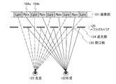
図5に、画素部101と、パララックスバリア120と、観察者の右目122と左目123の位置関係を示す。
FIG. 5 shows a positional relationship between the
図5では、画素部101が有する複数の画素のうち、任意の一走査線に接続された1行の画素を示している。上記1行の画素は、交互に配置された右目用画素104a(Rpix)と左目用画素104b(Lpix)とを含んでいる。
FIG. 5 illustrates one row of pixels connected to an arbitrary scanning line among a plurality of pixels included in the
また、図5では、光学系にパララックスバリア120を用いた例を示しており、パララックスバリア120には、光を遮る遮光部124と、光を通過させる開口部125とが交互に複数設けられている。そして、パララックスバリア120は、観察者の右目122及び左目123と画素部101とを結ぶ光の経路上に設けられている。
FIG. 5 shows an example in which a
画素部101の右目用画素104a(Rpix)と左目用画素104b(Lpix)とから発せられた光の一部は、パララックスバリア120の開口部125を通過し、観察者の右目122または左目123に入射する。そして、開口部125の形状または大きさと、画素部101のサイズと、右目122と左目123の距離とを最適化することで、右目用画素104a(Rpix)からの光を右目122に、左目用画素104b(Lpix)からの光を左目123に、選択的に入射させることができる。その結果、右目用画像と左目用画像とから構成される三次元画像を観察者に認識させることができる。
Part of the light emitted from the right-
なお、パララックスバリア120は、画素部101を有する液晶パネル内に形成されていても良い。
Note that the
次いで、光学系にレンチキュラーレンズを用いた場合について説明する。図6に、画素部101と、レンチキュラーレンズ130と、観察者の右目122と左目123の位置関係を示す。
Next, a case where a lenticular lens is used in the optical system will be described. FIG. 6 shows the positional relationship between the
図6では、図5と同様に、画素部101が有する複数の画素のうち、任意の一走査線に接続された1行の画素を示している。上記1行の画素は、交互に配置された右目用画素104a(Rpix)と左目用画素104b(Lpix)とを含んでいる。
In FIG. 6, similarly to FIG. 5, one row of pixels connected to one arbitrary scanning line among a plurality of pixels included in the
図7(A)にレンチキュラーレンズ130の斜視図を示す。レンチキュラーレンズ130は、蒲鉾型のレンズを複数連ねたような形状を有しており、半円形状の凸部において光が集光され、その進行方向が制御される。
FIG. 7A shows a perspective view of the
図6において、レンチキュラーレンズ130が有する凸部の長手方向は、一走査線が伸びている方向、すなわち右目用画素104a(Rpix)と左目用画素104b(Lpix)の配列方向と、交差している。そして、レンチキュラーレンズ130は、観察者の右目122及び左目123と画素部101とを結ぶ光の経路上に設けられている。
In FIG. 6, the longitudinal direction of the convex portion of the
画素部101の右目用画素104a(Rpix)と左目用画素104b(Lpix)とから発せられた光の一部は、レンチキュラーレンズ130によって集光され、観察者の右目122または左目123に入射する。そして、レンチキュラーレンズ130の焦点深度を最適化することで、右目用画素104a(Rpix)からの光を右目122に、左目用画素104b(Lpix)からの光を左目123に、選択的に入射させることができる。その結果、右目用画像と左目用画像とから構成される三次元画像を観察者に認識させることができる。
Part of the light emitted from the right-
なお、光学系にマイクロレンズアレイを用いる場合も、レンチキュラーレンズを用いる場合と同様に、レンズの各凸部において光が集光されることで、左目用画素104b(Lpix)からの光を左目123に、選択的に入射させることができる。
In the case where a microlens array is used in the optical system, similarly to the case where a lenticular lens is used, the light from the left-
図7(B)に、マイクロレンズアレイ140の斜視図を示す。マイクロレンズアレイ140は、複数の平凸レンズがマトリックス状に連なるように設けられている。
FIG. 7B shows a perspective view of the
レンチキュラーレンズやマイクロレンズアレイのように、光を遮蔽せずに有効に活用することができる光学系を用いることで、3次元画像の輝度が2次元画像の輝度よりも著しく低くなるのを防ぐことができる。 By using an optical system that can be used effectively without shielding light, such as a lenticular lens or a microlens array, the luminance of the three-dimensional image is prevented from becoming significantly lower than the luminance of the two-dimensional image. Can do.
一方、パララックスバリアは、上記レンチキュラーレンズやマイクロレンズアレイよりも画素に対する位置合わせが容易であり、また作製が容易である。 On the other hand, the parallax barrier is easier to align with the pixel and easier to manufacture than the lenticular lens and microlens array.
本発明の一態様に係る液晶表示装置は、画素部を複数の領域に分割し、領域ごとに異なる色相の光を順次供給することで、フルカラー画像の表示を行う。よって、特定の時刻に着目すると、隣接する領域に供給される光の色相を、互いに異ならせることができる。よって、各色の画像が合成されずに個別に視認されるのを防ぐことができ、FS駆動の場合とは異なり、動画の表示を行う際に起きやすかったカラーブレイクの発生を防ぐことができる。また、本発明の一態様に係る液晶表示装置は、カラーフィルタを用いる必要がないため、光供給部から発せられる光の利用効率を高めることができ、液晶表示装置全体の消費電力を低減させることができる。すなわち、本発明の一態様では、消費電力を低減できるというFS駆動のメリットを享受しつつ、カラーブレイクの発生というFS駆動のデメリットを防ぐことができる。 In a liquid crystal display device according to one embodiment of the present invention, a pixel portion is divided into a plurality of regions, and light of different hues is sequentially supplied to each region to display a full color image. Therefore, when paying attention to a specific time, the hue of light supplied to adjacent regions can be made different from each other. Therefore, it is possible to prevent the images of the respective colors from being individually viewed without being combined, and unlike the FS drive, it is possible to prevent the occurrence of a color break that is likely to occur when displaying a moving image. In addition, since the liquid crystal display device according to one embodiment of the present invention does not need to use a color filter, use efficiency of light emitted from the light supply portion can be increased and power consumption of the entire liquid crystal display device can be reduced. Can do. That is, according to one embodiment of the present invention, it is possible to prevent the demerit of FS driving such as occurrence of a color break while enjoying the merit of FS driving that power consumption can be reduced.
さらに、本発明の一態様では、1つの画素で各色に対応する画像の表示を行うことができるため、カラーフィルタ―方式に比べて高精細な画像の表示を行うことができる。よって、光学系を利用した三次元画像の表示方式を採用した場合であっても、各行において、画像の表示に寄与する画素数が低減するのを抑え、高精細な三次元画像の表示を行うことができる。 Further, according to one embodiment of the present invention, an image corresponding to each color can be displayed with one pixel, and thus a higher-definition image can be displayed compared to a color filter method. Therefore, even when a 3D image display method using an optical system is adopted, a reduction in the number of pixels contributing to image display in each row is suppressed, and a high-definition 3D image is displayed. be able to.
(実施の形態2)
本明細書において液晶表示装置とは、コントローラなどの外付け回路を含んでいても良い。本実施の形態では、本発明の一態様に係る液晶表示装置が有する、外付け回路の構成と、画素部の動作を制御する駆動回路の構成について、例を挙げて説明する。
(Embodiment 2)
In this specification, the liquid crystal display device may include an external circuit such as a controller. In this embodiment, an example of the structure of an external circuit and the structure of a driver circuit that controls operation of a pixel portion included in the liquid crystal display device according to one embodiment of the present invention will be described.
図8に、液晶表示装置400の構成を、一例としてブロック図で示す。なお、ブロック図では、構成要素を機能ごとに分類し、互いに独立したブロックとして示しているが、実際の構成要素は機能ごとに完全に切り分けることが難しく、一つの構成要素が複数の機能に係わることもあり得る。 FIG. 8 is a block diagram illustrating the configuration of the liquid crystal display device 400 as an example. In the block diagram, components are classified by function and shown as independent blocks. However, it is difficult to completely separate actual components by function, and one component is related to multiple functions. It can happen.
図8に示すように、本実施の形態の液晶表示装置400は、複数の画像メモリ401と、画像処理回路402と、コントローラ403と、液晶パネル404と、光供給部405と、光供給部制御回路406と、光学系407とを有する。
As shown in FIG. 8, the liquid crystal display device 400 of this embodiment includes a plurality of
液晶表示装置400には、フルカラー画像に対応する画像データ(フルカラー画像データ411)が入力される。画像処理回路402は、複数の画像メモリ401へのフルカラー画像データ411の書き込みと、複数の画像メモリ401からのフルカラー画像データ411の読み出しとを行う。フルカラー画像データ411には、複数の色相にそれぞれ対応する画像データが含まれている。複数の各画像メモリ401には、各色相に対応する画像データがそれぞれ記憶される。
The liquid crystal display device 400 receives image data (full color image data 411) corresponding to a full color image. The
画像メモリ401は、例えばDRAM(Dynamic Random Access Memory)、SRAM(Static Random Access Memory)等の記憶回路を用いることができる。或いは、画像メモリ401に、VRAM(Video RAM)を用いても良い。
As the
画像処理回路402から、複数の画像メモリ401に記憶されている、各色相に対応する画像データの読み出しは、コントローラ403からの命令に従って行われる。複数の画像メモリ401から読み出された各色相に対応する画像データは、液晶パネル404に送られる。
Reading of image data corresponding to each hue stored in the plurality of
また、コントローラ403は、フルカラー画像データ411に同期した駆動信号またはフルカラー画像の表示を行う際に用いられる電源電位を、液晶パネル404に供給する。
In addition, the controller 403 supplies the liquid crystal panel 404 with a driving signal synchronized with the full-
液晶パネル404は、各画素に液晶素子を有する画素部408と、信号線駆動回路409、走査線駆動回路410などの駆動回路とを有する。画素部408は、複数の表示領域を有している。図8では、画素部408が、第1表示領域420と第2表示領域421と第3の表示領域422とを有する場合を例示している。
The liquid crystal panel 404 includes a pixel portion 408 having a liquid crystal element in each pixel, and drive circuits such as a signal line driver circuit 409 and a scan
液晶パネル404に入力された各色相に対応する画像データは、信号線駆動回路409に与えられる。また、コントローラ403からの駆動信号または電源電位は、信号線駆動回路409または走査線駆動回路410に与えられる。
Image data corresponding to each hue input to the liquid crystal panel 404 is given to the signal line driver circuit 409. In addition, a drive signal or a power supply potential from the controller 403 is supplied to the signal line driver circuit 409 or the scan
なお、駆動信号には、信号線駆動回路409の動作を制御する信号線駆動回路用のスタートパルス信号SSP、信号線駆動回路用のクロック信号SCK、ラッチ信号LP、走査線駆動回路410の動作を制御する走査線駆動回路用のスタートパルス信号GSP、走査線駆動回路用のクロック信号GCK、パルス幅制御信号PWCなどが含まれる。
Note that the drive signal includes the start pulse signal SSP for the signal line driver circuit that controls the operation of the signal line driver circuit 409, the clock signal SCK for the signal line driver circuit, the latch signal LP, and the operation of the scanning
光供給部405には、色相の異なる光を発する複数の光源が設けられている。コントローラ403は、光供給部制御回路406を介して光供給部405が有する光源の駆動を制御する。 The light supply unit 405 is provided with a plurality of light sources that emit light having different hues. The controller 403 controls driving of the light source included in the light supply unit 405 via the light supply unit control circuit 406.
次いで、信号線駆動回路409の構成について説明する。図9に、信号線駆動回路409の構成を一例として示す。図9に示す信号線駆動回路409は、シフトレジスタ450、レベルシフタ451、デジタルバッファ452、第1記憶回路453、第2記憶回路454、アナログバッファ455を有している。
Next, the structure of the signal line driver circuit 409 is described. FIG. 9 illustrates a configuration example of the signal line driver circuit 409 as an example. A signal line driver circuit 409 illustrated in FIG. 9 includes a
信号線駆動回路409の動作について説明する。シフトレジスタ450に、スタートパルス信号SSPと、クロック信号SCKと、クロック信号SCKとは逆位相の電位を有するクロック信号SCKBとが入力されると、シフトレジスタ450は、パルスが順次シフトするタイミング信号を生成する。
The operation of the signal line driver circuit 409 will be described. When the start pulse signal SSP, the clock signal SCK, and the clock signal SCKB having a potential opposite in phase to the clock signal SCK are input to the
シフトレジスタ450から出力されたタイミング信号は、レベルシフタ451においてその電位の振幅が調整された後、デジタルバッファ452を介して第1記憶回路453に入力される。
The timing signal output from the
第1記憶回路453には、画像信号IMGが入力される。第1記憶回路453にタイミング信号が入力されると、該タイミング信号のパルスに従って、画像信号IMGがサンプリングされ、第1記憶回路453が有する複数の記憶素子に順に書き込まれる。すなわち、シリアルで信号線駆動回路409に入力された画像信号IMGが、第1記憶回路453にパラレルで書き込まれる。第1記憶回路453に書き込まれた画像信号IMGは、保持される。
The
なお、第1記憶回路453が有する複数の記憶素子に順に画像信号IMGを書き込んでも良いが、第1記憶回路453が有する複数の記憶素子をいくつかのグループに分け、該グループごとに並行して画像信号IMGを入力する、いわゆる分割駆動を行っても良い。なおこのときのグループ数を分割数と呼ぶ。例えば記憶素子を4つのグループに分けた場合、4分割で分割駆動することになる。
Note that the image signal IMG may be sequentially written to the plurality of memory elements included in the
第2記憶回路454には、ラッチ信号LPが入力される。第1記憶回路453への、画像信号IMGの書き込みが一通り終了した後、帰線期間において、第2記憶回路454に入力されるラッチ信号LPのパルスに従い、第1記憶回路453に保持されている画像信号IMGが、第2記憶回路454に一斉に書き込まれ、保持される。画像信号IMGを第2記憶回路454に送出し終えた第1記憶回路453では、再びシフトレジスタ450からのタイミング信号に従って、次の画像信号IMGの書き込みが順次行われる。この2順目の1ライン期間中には、第2記憶回路454に書き込まれ、保持されている画像信号IMGが、アナログバッファ455を介して信号線に送られる。
The latch signal LP is input to the
次いで、各走査線駆動回路410の構成について説明する。図10に、走査線駆動回路410の構成を一例として示す。図10に示す走査線駆動回路410は、シフトレジスタ460、セレクタ461、レベルシフタ462、デジタルバッファ463を有している。
Next, the configuration of each scanning
図11に示すタイミングチャートを用いて、図10に示す走査線駆動回路410の動作について説明する。走査線駆動回路410において、シフトレジスタ460は、スタートパルス信号GSPと、クロック信号GCKと、クロック信号GCKとは逆位相の電位を有するクロック信号GCKBとが入力されると、パルスが順次シフトする走査信号SROUTを生成する。
The operation of the scan
なお、図10では、シフトレジスタ460が、複数のフリップフロップGSRを有している場合を例示している。そして、複数のフリップフロップGSRのそれぞれから、走査信号SROUTが出力される。具体的には、初段のフリップフロップGSRから走査信号SROUT1が出力され、二段目のフリップフロップGSRから走査信号SROUT2が出力され、三段目のフリップフロップGSRから走査信号SROUT3が出力される。すなわち、シフトレジスタ460がy段のフリップフロップGSRを有しているならば、シフトレジスタ460から走査信号SROUT1乃至走査信号SROUTyが出力されることとなる。
Note that FIG. 10 illustrates a case where the
なお、図10では、複数の走査線駆動回路410の1つを例示しているが、液晶表示装置400が3つの走査線駆動回路410を有する場合、3つの各走査線駆動回路410が有するシフトレジスタ460から、それぞれ走査信号SROUTが出力される。例えば、一段目の走査線駆動回路410が有するシフトレジスタ460から、走査信号SROUT1乃至走査信号SROUTjが出力され、二段目の走査線駆動回路410が有するシフトレジスタ460から、走査信号SROUTj+1乃至走査信号SROUT2jが出力され、三段目の走査線駆動回路410が有するシフトレジスタ460から、走査信号SROUT2j+1乃至走査信号SROUT3jが出力される。
10 illustrates one of the plurality of scanning
シフトレジスタ460から出力された走査信号SROUTは、セレクタ461に入力される。また、セレクタ461には、パルス幅制御信号PWCも入力されている。セレクタ461は、走査信号SROUTのパルスに従って、パルス幅制御信号PWCの電位の出力を制御することで、選択信号Goutを生成する。
The scanning signal SROUT output from the
なお、図10では、複数の走査線駆動回路410の1つを例示しているが、液晶表示装置400が3つの走査線駆動回路410を有する場合、図11に示すように、パルス幅制御信号PWC1乃至パルス幅制御信号PWC6を用いる。
FIG. 10 illustrates one of the plurality of scanning
具体的に、図11では、一段目の走査線駆動回路410が有するセレクタ461に、パルス幅制御信号PWC1及びパルス幅制御信号PWC4が入力される。また、一段目の走査線駆動回路410が有するセレクタ461は、複数のセレクタSELを有しており、上記複数の各セレクタSELには、パルス幅制御信号PWC1とパルス幅制御信号PWC4のいずれか一方が入力される。上記構成により、一段目の走査線駆動回路410が有するセレクタ461において、選択信号Gout1乃至選択信号Goutjが生成される。
Specifically, in FIG. 11, the pulse width control signal PWC1 and the pulse width control signal PWC4 are input to the
同様に、二段目の走査線駆動回路410が有するセレクタ461に、パルス幅制御信号PWC2及びパルス幅制御信号PWC5が入力される。また、二段目の走査線駆動回路410が有するセレクタ461は、複数のセレクタSELを有しており、上記複数の各セレクタSELには、パルス幅制御信号PWC2とパルス幅制御信号PWC5のいずれか一方が入力される。上記構成により、二段目の走査線駆動回路410が有するセレクタ461において、選択信号Goutj+1乃至選択信号Gout2jが生成される。
Similarly, the pulse width control signal PWC2 and the pulse width control signal PWC5 are input to the
同様に、三段目の走査線駆動回路410が有するセレクタ461に、パルス幅制御信号PWC3及びパルス幅制御信号PWC6が入力される。また、三段目の走査線駆動回路410が有するセレクタ461は、複数のセレクタSELを有しており、上記複数の各セレクタSELには、パルス幅制御信号PWC3とパルス幅制御信号PWC6のいずれか一方が入力される。上記構成により、三段目の走査線駆動回路410が有するセレクタ461において、選択信号Gout2j+1乃至選択信号Gout3jが生成される。
Similarly, the pulse width control signal PWC3 and the pulse width control signal PWC6 are input to the
セレクタ461において生成された選択信号Goutは、レベルシフタ462においてその電位の振幅が調整された後、デジタルバッファ463を介して画素部408の走査線に入力される。
The selection signal Gout generated in the
具体的には、選択信号Gout1乃至選択信号Goutjが、第1表示領域420が有する走査線G1乃至走査線Gjにそれぞれ入力される。選択信号Goutj+1乃至選択信号Gout2jが、第2表示領域421が有する走査線Gj+1乃至走査線G2jにそれぞれ入力される。選択信号Gout2j+1乃至選択信号Gout3jが、第3表示領域422が有する走査線G2j+1乃至走査線G3jにそれぞれ入力される。
Specifically, the selection signals Gout1 to Goutj are input to the scanning lines G1 to Gj included in the
画素部408が有する画素は、走査線駆動回路410から入力された選択信号Goutにより選択される。信号線駆動回路409から信号線を介して画素部408に送られた画像信号IMGは、上記選択された画素に入力される。
A pixel included in the pixel portion 408 is selected by a selection signal Gout input from the scan
本実施の形態は、上記実施の形態と適宜組み合わせて実施することが可能である。 This embodiment can be implemented in combination with any of the above embodiments as appropriate.
(実施の形態3)
本実施の形態では、図2に示す画素104の、具体的な構成について説明する。
(Embodiment 3)
In this embodiment, a specific structure of the
図12(A)に、画素の上面図を一例として示す。また、図12(B)に、図12(A)の破線A1―A2、及び破線B1−B2における断面図を示す。 FIG. 12A illustrates a top view of a pixel as an example. FIG. 12B is a cross-sectional view taken along dashed lines A1-A2 and B1-B2 in FIG.
図12(A)、図12(B)に示す画素は、導電膜501が、走査線G、またはトランジスタ107のゲート電極として機能する。また、導電膜502は、信号線S、またはトランジスタ107の第1端子として機能する。導電膜503は、容量素子108が有する電極の一つとして機能する。導電膜504は、トランジスタ107の第2端子、または容量素子108が有する電極の別の一つとして機能する。
In the pixel illustrated in FIGS. 12A and 12B, the
導電膜501、導電膜503上にはゲート絶縁膜506が形成されている。トランジスタ107の活性層507は、導電膜501と重なる位置においてゲート絶縁膜506上に形成されている。
A
また、図12(A)、図12(B)に示す画素では、導電膜503と導電膜502とが重なる位置において、ゲート絶縁膜506及び半導体膜520が設けられている。具体的には、導電膜503上にゲート絶縁膜506が設けられ、ゲート絶縁膜506上に半導体膜520が設けられ、半導体膜520上に導電膜502が設けられている。半導体膜520を導電膜502と導電膜503の間に設けることで、導電膜502と導電膜503の間に形成される寄生容量を小さく抑えることができる。
In the pixel illustrated in FIGS. 12A and 12B, the
また、図12(A)、図12(B)に示す画素では、導電膜501と導電膜502とが重なる位置において、ゲート絶縁膜506及び半導体膜523が設けられている。具体的には、導電膜501上にゲート絶縁膜506が設けられ、ゲート絶縁膜506上に半導体膜523が設けられ、半導体膜523上に導電膜502が設けられている。半導体膜523を導電膜501と導電膜502の間に設けることで、導電膜501と導電膜502の間に形成される寄生容量を小さく抑えることができる。
In the pixel illustrated in FIGS. 12A and 12B, the
なお、導電膜501、導電膜503は、絶縁表面を有する基板500上に形成された一の導電膜を所望の形状に加工することで形成することができる。活性層507、半導体膜520、半導体膜523は、ゲート絶縁膜506上に形成された一の半導体膜を所望の形状に加工することで形成することができる。導電膜502、導電膜504は、ゲート絶縁膜506、活性層507、半導体膜520及び半導体膜523上に形成された一の導電膜を所望の形状に加工することで形成することができる。
Note that the
さらに、図12(A)、図12(B)に示す画素は、活性層507、半導体膜520、半導体膜523、導電膜502、導電膜504を覆うように、絶縁膜512が形成されている。そして、絶縁膜512に形成されたコンタクトホールを介して導電膜504と接するように、絶縁膜512上に導電膜521が形成されている。そして、導電膜521及び絶縁膜512上に、絶縁膜513が形成されている。そして、絶縁膜513上には画素電極505が形成されており、絶縁膜513に形成されたコンタクトホールを介して、導電膜521と画素電極505とが接している。
Further, in the pixel illustrated in FIGS. 12A and 12B, an insulating
なお、図12(A)、図12(B)に示す画素では、導電膜504と画素電極505が、導電膜521を介して接続されているが、本発明の一態様では、導電膜521を設けずに、導電膜504と画素電極505が接する構成であっても良い。
Note that in the pixel illustrated in FIGS. 12A and 12B, the
導電膜503と、導電膜504とが、ゲート絶縁膜506を間に挟んで重なり合っている部分が、容量素子108として機能する。
A portion where the
また、本実施の形態では、導電膜521と画素電極505とが重なる位置において、画素電極505上にスペーサ510が形成されている。
In this embodiment mode, the
なお、図12(A)では、スペーサ510までが形成された画素の上面図を示している。図12(B)では、スペーサ510までが形成されている基板500と対峙するように、基板514が配置されている様子を示す。
Note that FIG. 12A shows a top view of a pixel in which the
基板514上には対向電極515が形成されており、画素電極505と対向電極515の間には液晶を含む液晶層516が設けられている。画素電極505と、対向電極515と、液晶層516とが重なる部分に液晶素子106が形成される。
A
透過型の液晶表示装置である場合、画素電極505と対向電極515には、例えば、酸化珪素を含む酸化インジウムスズ(ITSO)、酸化インジウムスズ(ITO)、酸化亜鉛(ZnO)、酸化インジウム亜鉛、ガリウムを添加した酸化亜鉛(GZO)などの透光性を有する導電材料を用いることができる。反射型の液晶表示装置である場合は、対向電極515に、光を反射もしくは遮蔽する材料、例えば、窒化チタン、窒化ジルコニウム、チタン、タングステン、ニッケル、白金、クロム、銀、アルミニウム等を用いることができる。
In the case of a transmissive liquid crystal display device, the
なお、画素電極505と液晶層516の間、または対向電極515と液晶層516の間に、配向膜を適宜設けても良い。配向膜は、ポリイミド、ポリビニルアルコールなどの有機樹脂を用いて形成することができ、その表面には、ラビングなどの、液晶分子を一定方向に配列させるための配向処理が施されている。ラビングは、配向膜に接するように、ナイロンなどの布を巻いたローラーを回転させて、上記配向膜の表面を一定方向に擦ることで、行うことができる。なお、酸化珪素などの無機材料を用い、配向処理を施すことなく、蒸着法で配向特性を有する配向膜を直接形成することも可能である。
Note that an alignment film may be provided as appropriate between the
また、液晶層516を形成するために行われる液晶の注入は、ディスペンサ式(滴下式)を用いても良いし、ディップ式(汲み上げ式)を用いていても良い。
In addition, liquid crystal injection performed for forming the
なお、基板514上には、画素間における液晶の配向の乱れに起因するディスクリネーションが視認されるのを防ぐため、或いは、拡散した光が隣接する複数の画素に入射するのを防ぐために、光を遮蔽することができる遮蔽膜517が設けられている。遮蔽膜517には、カーボンブラック、二酸化チタンよりも酸化数が小さい低次酸化チタンなどの黒色顔料を含む有機樹脂を用いることができる。または、クロムを用いた膜で、遮蔽膜を形成することも可能である。
Note that on the
なお、図12では、画素電極505と対向電極515の間に液晶層516が挟まれている構造を有する液晶素子106を例に挙げて説明したが、本発明の一態様に係る液晶表示装置はこの構成に限定されない。IPS型の液晶素子やブルー相を用いた液晶素子のように、一対の電極が共に一の基板に形成されていても良い。
Note that although the
次いで、液晶素子が有する液晶層にブルー相を示す液晶を用いた場合の、図2に示す画素104の具体的な構成について説明する。
Next, a specific structure of the
図13(A)に、画素の上面図を一例として示す。また、図13(B)に、図13(A)の破線C1―C2における断面図を示す。 FIG. 13A illustrates a top view of a pixel as an example. FIG. 13B is a cross-sectional view taken along dashed line C1-C2 in FIG.
図13(A)、図13(B)に示す画素は、導電膜601が、走査線G、またはトランジスタ107のゲート電極として機能する。また、導電膜602は、信号線S、またはトランジスタ107の第1端子として機能する。導電膜603は、容量素子108が有する電極の一つとして機能する。導電膜604は、トランジスタ107の第2端子、または容量素子108が有する電極の別の一つとして機能する。
In the pixel illustrated in FIGS. 13A and 13B, the
導電膜601、導電膜603上にはゲート絶縁膜606が形成されている。トランジスタ107の活性層607は、導電膜601と重なる位置においてゲート絶縁膜606上に形成されている。さらに、活性層607、導電膜602、導電膜604を覆うように、絶縁膜612と、絶縁膜613とが順に形成されている。そして、絶縁膜613上には画素電極605及び共通電極608が形成されており、絶縁膜612及び絶縁膜613に形成されたコンタクトホールを介して、導電膜604と画素電極605とが接続されている。
A
導電膜601、導電膜603は、絶縁表面を有する基板600上に形成された一の導電膜を所望の形状に加工することで形成することができる。導電膜601、導電膜603上にはゲート絶縁膜606が形成されている。導電膜602、導電膜604は、活性層607及びゲート絶縁膜606上に形成された一の導電膜を所望の形状に加工することで形成することができる。
The
なお、導電膜603と、導電膜604とが、ゲート絶縁膜606を間に挟んで重なり合っている部分が、容量素子108として機能する。
Note that a portion where the
また、図13(A)及び図13(B)に示す画素では、導電膜603とゲート絶縁膜606の間に絶縁膜609が形成されている。そして、画素電極605と絶縁膜609とが重なる位置において、画素電極605上にスペーサ610が形成されている。
In the pixel illustrated in FIGS. 13A and 13B, an insulating
なお、図13(A)では、スペーサ610までが形成された画素の上面図を示している。図13(B)では、スペーサ610までが形成されている基板600と対峙するように、基板614が配置されている様子を示す。
Note that FIG. 13A illustrates a top view of a pixel in which the
基板614と、画素電極605及び共通電極608との間には、液晶を含む液晶層616が設けられている。画素電極605と、共通電極608と、液晶層616とを含む領域に液晶素子106が形成される。
A
画素電極605と共通電極608には、例えば、酸化珪素を含む酸化インジウムスズ(ITSO)、酸化インジウムスズ(ITO)、酸化亜鉛(ZnO)、酸化インジウム亜鉛、ガリウムを添加した酸化亜鉛(GZO)などの透光性を有する導電材料を用いることができる。
The
液晶層616を形成するために行われる液晶の注入は、ディスペンサ式(滴下式)を用いても良いし、ディップ式(汲み上げ式)を用いていても良い。
The liquid crystal injection performed to form the
なお、基板614上には、画素間における液晶の配向の乱れに起因するディスクリネーションが視認されるのを防ぐため、或いは、拡散した光が隣接する複数の画素に入射するのを防ぐために、光を遮蔽することができる遮蔽膜が設けられていても良い。遮蔽膜には、カーボンブラック、二酸化チタンよりも酸化数が小さい低次酸化チタンなどの黒色顔料を含む有機樹脂を用いることができる。または、クロムを用いた膜で、遮蔽膜を形成することも可能である。
Note that, on the
なお、図12または図13において、トランジスタ107は、酸化物半導体などのワイドギャップ半導体を活性層507或いは活性層607に有していても良いし、非晶質、微結晶、多結晶又は単結晶である、シリコン又はゲルマニウムなどの半導体を活性層507或いは活性層607に有していても良い。
12 or 13, the
酸化物半導体は、シリコンよりもバンドギャップが広く、真性キャリア密度がシリコンよりも低いため、酸化物半導体をトランジスタの活性層に用いることで、通常のシリコンやゲルマニウムなどの半導体を活性層に有するトランジスタに比べて、オフ電流が極めて低いトランジスタを実現することができる。 Since an oxide semiconductor has a wider band gap and lower intrinsic carrier density than silicon, an oxide semiconductor is used for an active layer of a transistor, so that a transistor having a normal semiconductor such as silicon or germanium in an active layer is used. In comparison with the transistor, a transistor with extremely low off-state current can be realized.
なお、電子供与体(ドナー)となる水分又は水素などの不純物が低減され、なおかつ酸素欠損が低減されることで高純度化された酸化物半導体(purified Oxide Semiconductor)は、i型(真性半導体)又はi型に限りなく近い。そのため、上記酸化物半導体を用いたトランジスタは、オフ電流が著しく低いという特性を有する。具体的に、高純度化された酸化物半導体は、二次イオン質量分析法(SIMS:Secondary Ion Mass Spectroscopy)による水素濃度の測定値が、5×10¹⁹/cm3以下、好ましくは5×1018/cm3以下、より好ましくは5×1017/cm3以下、更に好ましくは1×1016/cm3以下とする。また、ホール効果測定により測定できる酸化物半導体膜のキャリア密度は、1×1014/cm3未満、好ましくは1×1012/cm3未満、更に好ましくは1×1011/cm3未満とする。また、酸化物半導体のバンドギャップは、2eV以上、好ましくは2.5eV以上、より好ましくは3eV以上である。水分又は水素などの不純物濃度が十分に低減され、なおかつ酸素欠損が低減されることで高純度化された酸化物半導体膜を用いることにより、トランジスタのオフ電流を下げることができる。 Note that an oxide semiconductor that is highly purified by reducing impurities such as moisture or hydrogen serving as an electron donor (donor) and reducing oxygen vacancies is an i-type (intrinsic semiconductor). Or it is close to i type. Therefore, a transistor including the above oxide semiconductor has a characteristic of extremely low off-state current. Specifically, a highly purified oxide semiconductor has a hydrogen concentration measured by secondary ion mass spectrometry (SIMS) of 5 × 10 19 / cm 3 or less, preferably 5 × 10. 18 / cm 3 or less, more preferably 5 × 10 17 / cm 3 or less, and even more preferably 1 × 10 16 / cm 3 or less. The carrier density of the oxide semiconductor film that can be measured by Hall effect measurement is less than 1 × 10 14 / cm 3 , preferably less than 1 × 10 12 / cm 3 , and more preferably less than 1 × 10 11 / cm 3 . . The band gap of the oxide semiconductor is 2 eV or more, preferably 2.5 eV or more, more preferably 3 eV or more. By using an oxide semiconductor film which is highly purified by sufficiently reducing the concentration of impurities such as moisture or hydrogen and reducing oxygen vacancies, the off-state current of the transistor can be reduced.
ここで、酸化物半導体膜中の、水素濃度の分析について触れておく。半導体膜中の水素濃度測定は、SIMSで行う。SIMSは、その原理上、試料表面近傍や、材質が異なる膜との積層界面近傍のデータを正確に得ることが困難であることが知られている。そこで、膜中における水素濃度の厚さ方向の分布をSIMSで分析する場合、対象となる膜が存在する範囲において、値に極端な変動がなく、ほぼ一定の値が得られる領域における平均値を、水素濃度として採用する。また、測定の対象となる膜の厚さが小さい場合、隣接する膜内の水素濃度の影響を受けて、ほぼ一定の値が得られる領域を見いだせない場合がある。この場合、当該膜が存在する領域における、水素濃度の極大値又は極小値を、当該膜中の水素濃度として採用する。更に、当該膜が存在する領域において、極大値を有する山型のピーク、極小値を有する谷型のピークが存在しない場合、変曲点の値を水素濃度として採用する。 Here, the analysis of the hydrogen concentration in the oxide semiconductor film is mentioned. The hydrogen concentration in the semiconductor film is measured by SIMS. In SIMS, it is known that it is difficult to accurately obtain data in the vicinity of the sample surface and in the vicinity of the laminated interface with films of different materials. Therefore, when analyzing the distribution of the hydrogen concentration in the film in the thickness direction by SIMS, the average value in a region where there is no extreme variation in the value and an almost constant value can be obtained in the range where the target film exists. Adopted as hydrogen concentration. Further, when the thickness of the film to be measured is small, there may be a case where an area where a substantially constant value is obtained cannot be found due to the influence of the hydrogen concentration in the adjacent film. In this case, the maximum value or the minimum value of the hydrogen concentration in the region where the film is present is adopted as the hydrogen concentration in the film. Furthermore, in the region where the film is present, when there is no peak having a maximum value and no valley peak having a minimum value, the value of the inflection point is adopted as the hydrogen concentration.
具体的に、高純度化された酸化物半導体膜を活性層として用いたトランジスタのオフ電流が低いことは、いろいろな実験により証明できる。例えば、チャネル幅が1×106μmでチャネル長が10μmの、酸化物半導体膜を活性層として用いたトランジスタであっても、ソース端子とドレイン端子間の電圧(ドレイン電圧)が1Vから10Vの範囲において、オフ電流が、半導体パラメータアナライザの測定限界以下、すなわち1×10⁻¹³A以下という特性を得ることができる。この場合、オフ電流をトランジスタのチャネル幅で除した数値に相当するオフ電流密度は、100zA/μm以下であることが分かる。 Specifically, it can be proved by various experiments that the off-state current of a transistor using a highly purified oxide semiconductor film as an active layer is low. For example, even in a transistor using an oxide semiconductor film as an active layer and having a channel width of 1 × 10 6 μm and a channel length of 10 μm, the voltage between the source terminal and the drain terminal (drain voltage) is 1V to 10V. In the range, it is possible to obtain a characteristic that the off-current is below the measurement limit of the semiconductor parameter analyzer, that is, 1 × 10 −13 A or less. In this case, it can be seen that the off-current density corresponding to a value obtained by dividing the off-current by the channel width of the transistor is 100 zA / μm or less.
なお、酸化物半導体としては、少なくともインジウム(In)あるいは亜鉛(Zn)を含むことが好ましい。特にInとZnを含むことが好ましい。また、該酸化物を用いたトランジスタの電気的特性のばらつきを減らすためのスタビライザーとして、それらに加えてガリウム(Ga)を有することが好ましい。また、スタビライザーとしてスズ(Sn)を有することが好ましい。また、スタビライザーとしてハフニウム(Hf)を有することが好ましい。また、スタビライザーとしてアルミニウム(Al)を有することが好ましい。 Note that the oxide semiconductor preferably contains at least indium (In) or zinc (Zn). In particular, In and Zn are preferably included. In addition, it is preferable to include gallium (Ga) in addition to the stabilizer for reducing variation in electrical characteristics of the transistor including the oxide. Moreover, it is preferable to have tin (Sn) as a stabilizer. Moreover, it is preferable to have hafnium (Hf) as a stabilizer. Moreover, it is preferable to have aluminum (Al) as a stabilizer.
また、他のスタビライザーとして、ランタノイドである、ランタン(La)、セリウム(Ce)、プラセオジム(Pr)、ネオジム(Nd)、サマリウム(Sm)、ユウロピウム(Eu)、ガドリニウム(Gd)、テルビウム(Tb)、ジスプロシウム(Dy)、ホルミウム(Ho)、エルビウム(Er)、ツリウム(Tm)、イッテルビウム(Yb)、ルテチウム(Lu)のいずれか一種または複数種を含んでいてもよい。 As other stabilizers, lanthanoids such as lanthanum (La), cerium (Ce), praseodymium (Pr), neodymium (Nd), samarium (Sm), europium (Eu), gadolinium (Gd), terbium (Tb) , Dysprosium (Dy), holmium (Ho), erbium (Er), thulium (Tm), ytterbium (Yb), or lutetium (Lu) may be included.
例えば、酸化物半導体として、酸化インジウム、酸化スズ、酸化亜鉛、二元系金属の酸化物であるIn−Zn系酸化物、Sn−Zn系酸化物、Al−Zn系酸化物、Zn−Mg系酸化物、Sn−Mg系酸化物、In−Mg系酸化物、In−Ga系酸化物、三元系金属の酸化物であるIn−Ga−Zn系酸化物(IGZOとも表記する)、In−Al−Zn系酸化物、In−Sn−Zn系酸化物、Sn−Ga−Zn系酸化物、Al−Ga−Zn系酸化物、Sn−Al−Zn系酸化物、In−Hf−Zn系酸化物、In−La−Zn系酸化物、In−Ce−Zn系酸化物、In−Pr−Zn系酸化物、In−Nd−Zn系酸化物、In−Sm−Zn系酸化物、In−Eu−Zn系酸化物、In−Gd−Zn系酸化物、In−Tb−Zn系酸化物、In−Dy−Zn系酸化物、In−Ho−Zn系酸化物、In−Er−Zn系酸化物、In−Tm−Zn系酸化物、In−Yb−Zn系酸化物、In−Lu−Zn系酸化物、四元系金属の酸化物であるIn−Sn−Ga−Zn系酸化物、In−Hf−Ga−Zn系酸化物、In−Al−Ga−Zn系酸化物、In−Sn−Al−Zn系酸化物、In−Sn−Hf−Zn系酸化物、In−Hf−Al−Zn系酸化物を用いることができる。また、上記酸化物半導体は、珪素を含んでいてもよい。 For example, as an oxide semiconductor, indium oxide, tin oxide, zinc oxide, binary metal oxides such as In—Zn oxide, Sn—Zn oxide, Al—Zn oxide, Zn—Mg oxide Oxides, Sn—Mg oxides, In—Mg oxides, In—Ga oxides, In—Ga—Zn oxides (also referred to as IGZO) which are oxides of ternary metals, In— Al-Zn oxide, In-Sn-Zn oxide, Sn-Ga-Zn oxide, Al-Ga-Zn oxide, Sn-Al-Zn oxide, In-Hf-Zn oxide In-La-Zn-based oxide, In-Ce-Zn-based oxide, In-Pr-Zn-based oxide, In-Nd-Zn-based oxide, In-Sm-Zn-based oxide, In-Eu -Zn oxide, In-Gd-Zn oxide, In-Tb-Zn oxide, n-Dy-Zn-based oxide, In-Ho-Zn-based oxide, In-Er-Zn-based oxide, In-Tm-Zn-based oxide, In-Yb-Zn-based oxide, In-Lu-Zn -Based oxides, In-Sn-Ga-Zn-based oxides that are oxides of quaternary metals, In-Hf-Ga-Zn-based oxides, In-Al-Ga-Zn-based oxides, In-Sn- An Al—Zn-based oxide, an In—Sn—Hf—Zn-based oxide, or an In—Hf—Al—Zn-based oxide can be used. The oxide semiconductor may contain silicon.
なお、例えば、In−Ga−Zn系酸化物とは、InとGaとZnを含む酸化物という意味であり、InとGaとZnの比率は問わない。また、InとGaとZn以外の金属元素を含んでいてもよい。In−Ga−Zn系酸化物は、無電界時の抵抗が十分に高くオフ電流を十分に小さくすることが可能であり、また、移動度も高いため、半導体装置に用いる半導体材料としては好適である。 Note that for example, an In—Ga—Zn-based oxide means an oxide containing In, Ga, and Zn, and there is no limitation on the ratio of In, Ga, and Zn. Moreover, metal elements other than In, Ga, and Zn may be included. An In—Ga—Zn-based oxide has a sufficiently high resistance in the absence of an electric field and can have a sufficiently low off-state current. Also, since it has high mobility, it is suitable as a semiconductor material used for a semiconductor device. is there.
例えば、In:Ga:Zn=1:1:1(=1/3:1/3:1/3)あるいはIn:Ga:Zn=2:2:1(=2/5:2/5:1/5)の原子比のIn−Ga−Zn系酸化物やその組成の近傍の酸化物を用いることができる。あるいは、In:Sn:Zn=1:1:1(=1/3:1/3:1/3)、In:Sn:Zn=2:1:3(=1/3:1/6:1/2)あるいはIn:Sn:Zn=2:1:5(=1/4:1/8:5/8)の原子比のIn−Sn−Zn系酸化物やその組成の近傍の酸化物を用いるとよい。 For example, In: Ga: Zn = 1: 1: 1 (= 1/3: 1/3: 1/3) or In: Ga: Zn = 2: 2: 1 (= 2/5: 2/5: 1). / 5) atomic ratio In—Ga—Zn-based oxides and oxides in the vicinity of the composition can be used. Alternatively, In: Sn: Zn = 1: 1: 1 (= 1/3: 1/3: 1/3), In: Sn: Zn = 2: 1: 3 (= 1/3: 1/6: 1) / 2) or In: Sn: Zn = 2: 1: 5 (= 1/4: 1/8: 5/8) atomic ratio In—Sn—Zn-based oxide or an oxide in the vicinity of the composition. Use it.
しかし、これらに限られず、必要とする半導体特性(移動度、しきい値、ばらつき等)に応じて適切な組成のものを用いればよい。また、必要とする半導体特性を得るために、キャリア密度や不純物濃度、欠陥密度、金属元素と酸素の原子数比、原子間結合距離、密度等を適切なものとすることが好ましい。 However, the composition is not limited thereto, and a material having an appropriate composition may be used depending on required semiconductor characteristics (mobility, threshold value, variation, etc.). In order to obtain the required semiconductor characteristics, it is preferable that the carrier density, impurity concentration, defect density, atomic ratio of metal element to oxygen, interatomic bond distance, density, and the like be appropriate.
例えば、In−Sn−Zn系酸化物では比較的容易に高い移動度が得られる。しかしながら、In−Ga−Zn系酸化物でも、バルク内欠陥密度を低減することにより移動度を上げることができる。 For example, high mobility can be obtained relatively easily with an In—Sn—Zn-based oxide. However, mobility can be increased by reducing the defect density in the bulk also in the case of using an In—Ga—Zn-based oxide.
なお、例えば、In、Ga、Znの原子数比がIn:Ga:Zn=a:b:c(a+b+c=1)である酸化物の組成が、原子数比がIn:Ga:Zn=A:B:C(A+B+C=1)の酸化物の組成の近傍であるとは、a、b、cが、(a―A)2+(b―B)2+(c―C)2≦r2を満たすことを言い、rは、例えば、0.05とすればよい。他の酸化物でも同様である。 Note that for example, the composition of an oxide in which the atomic ratio of In, Ga, and Zn is In: Ga: Zn = a: b: c (a + b + c = 1) has an atomic ratio of In: Ga: Zn = A: B: being in the vicinity of the oxide composition of C (A + B + C = 1), a, b and c are (a−A) 2 + (b−B) 2 + (c−C) 2 ≦ r 2 R may be 0.05, for example. The same applies to other oxides.
なお、特に断りがない限り、本明細書でオフ電流とは、nチャネル型トランジスタにおいては、ドレイン端子をソース端子とゲート電極よりも高い電位とした状態において、ソース端子の電位を基準としたときのゲート端子の電位が0以下であるときに、ソース端子とドレイン端子の間に流れる電流のことを意味する。或いは、本明細書でオフ電流とは、pチャネル型トランジスタにおいては、ドレイン端子をソース端子とゲート電極よりも低い電位とした状態において、ソース端子の電位を基準としたときのゲート電極の電位が0以上であるときに、ソース端子とドレイン端子の間に流れる電流のことを意味する。 Note that unless otherwise specified, off-state current in this specification refers to an n-channel transistor in which the drain terminal is higher than the source terminal and the gate electrode, and the potential of the source terminal is used as a reference. This means a current that flows between the source terminal and the drain terminal when the potential of the gate terminal is 0 or less. Alternatively, in this specification, off-state current refers to that in a p-channel transistor, the potential of the gate electrode with respect to the potential of the source terminal in a state where the drain terminal is lower than the source terminal and the gate electrode. When it is 0 or more, it means a current flowing between the source terminal and the drain terminal.
また、シリコンよりもバンドギャップが広く、真性キャリア密度がシリコンよりも低い半導体材料の一例として、酸化物半導体の他に、炭化シリコン(SiC)、窒化ガリウム(GaN)などの化合物半導体を挙げることができる。酸化物半導体は、炭化シリコンや窒化ガリウムなどの化合物半導体とは異なり、スパッタリング法や湿式法などにより作製可能であり、量産性に優れるといった利点がある。また、炭化シリコンまたは窒化ガリウムとは異なり、酸化物半導体は室温でも成膜が可能なため、ガラス基板上への成膜、或いはシリコンを用いた集積回路上への成膜が可能である。また、酸化物半導体は、多結晶シリコン、微結晶シリコンなどの結晶性を有するシリコンや、炭化シリコン、窒化ガリウムなどとは異なり、第6世代以上の大型基板への対応が可能である。よって、酸化物半導体は量産性が高いというメリットを特に有する。また、トランジスタの性能(例えば電界効果移動度)を向上させるために結晶性の酸化物半導体を得ようとする場合でも、250℃から800℃の熱処理によって容易に結晶性の酸化物半導体を得ることができる。 In addition to oxide semiconductors, compound semiconductors such as silicon carbide (SiC) and gallium nitride (GaN) are given as examples of semiconductor materials having a wider band gap and lower intrinsic carrier density than silicon. it can. Unlike compound semiconductors such as silicon carbide and gallium nitride, an oxide semiconductor can be manufactured by a sputtering method, a wet method, or the like, and has an advantage of excellent mass productivity. In addition, unlike silicon carbide or gallium nitride, an oxide semiconductor can be formed at room temperature; therefore, it can be formed over a glass substrate or over an integrated circuit using silicon. In addition, an oxide semiconductor, unlike silicon having crystallinity such as polycrystalline silicon or microcrystalline silicon, silicon carbide, gallium nitride, or the like, can be applied to a large substrate of the sixth generation or higher. Therefore, an oxide semiconductor particularly has a merit that mass productivity is high. Even when a crystalline oxide semiconductor is obtained in order to improve transistor performance (eg, field effect mobility), a crystalline oxide semiconductor can be easily obtained by heat treatment at 250 ° C. to 800 ° C. Can do.
液晶表示装置では、画像信号の電位の極性を、共通電極の電位を基準として反転させる反転駆動を行うことで、焼き付きと呼ばれる液晶の劣化を防ぐことができる。しかし、反転駆動を行うと、画像信号の極性が変化する際に信号線に与えられる電位の変化が大きくなるため、スイッチング素子として機能するトランジスタ107のソース端子とドレイン端子の電位差が大きくなる。特に、ブルー相を示す液晶を液晶層が含んでいる場合は上記電位差が非常に大きくなる。例えばTN液晶を液晶層に含んでいる場合だと、上記電位差が十数V程度であるのに対し、ブルー相を示す液晶を液晶層が含んでいる場合は、上記電位差が数十Vにも及ぶ。よって、トランジスタ107は、閾値電圧がシフトするなどの特性劣化が生じやすい。また、液晶素子に保持されている電圧を維持するために、ソース端子とドレイン端子の電位差が大きくても、オフ電流が低いことが要求される。トランジスタ107に、シリコンまたはゲルマニウムよりもバンドギャップが大きく、真性キャリア密度が低い酸化物半導体などの半導体を用いることで、トランジスタ107の耐圧性を高め、オフ電流を著しく低くすることができる。よって、通常のシリコンやゲルマニウムなどの半導体材料で形成されたトランジスタを用いた場合に比べて、トランジスタ107の劣化を防ぎ、液晶素子に保持されている電圧を維持することができる。
In the liquid crystal display device, deterioration of the liquid crystal called burn-in can be prevented by performing inversion driving in which the polarity of the potential of the image signal is inverted with respect to the potential of the common electrode. However, when inversion driving is performed, a change in potential applied to the signal line when the polarity of the image signal changes increases, so that a potential difference between the source terminal and the drain terminal of the
なお、トランジスタ107は、活性層507或いは活性層607の片側にだけ存在するゲート電極を少なくとも有していれば良いが、活性層507或いは活性層607を間に挟んで存在する一対のゲート電極を有していても良い。また、トランジスタ107は、単数のゲート電極と単数のチャネル形成領域を有するシングルゲート構造であっても良いし、電気的に接続された複数のゲート電極を有することで、チャネル形成領域を複数有する、マルチゲート構造であっても良い。
Note that the
また、導電膜501乃至導電膜504と、導電膜521と、導電膜601乃至導電膜604とは、アルミニウム、クロム、銅、タンタル、チタン、モリブデン、タングステンから選ばれた元素、又は上述した元素を成分とする合金か、上述した元素を組み合わせた合金膜等が挙げられる。また、アルミニウム、銅などの金属膜の下側もしくは上側にクロム、タンタル、チタン、モリブデン、タングステンなどの高融点金属膜を積層させた構成としても良い。また、アルミニウム又は銅は、耐熱性や腐食性の問題を回避するために、高融点金属材料と組み合わせて用いると良い。高融点金属材料としては、モリブデン、チタン、クロム、タンタル、タングステン、ネオジム、スカンジウム、イットリウム等を用いることができる。また、Cu−Mg−Al合金、Mo−Ti合金、Ti、Mo、は、酸化膜との密着性が高い。よって、下層にCu−Mg−Al合金、Mo−Ti合金、Ti、或いはMoで構成される導電膜、上層にCuで構成される導電膜を積層し、上記積層された導電膜を導電膜501乃至導電膜504と、導電膜521と、導電膜601乃至導電膜604とに用いることで、酸化膜である絶縁膜と、導電膜501乃至導電膜504と、導電膜521と、導電膜601乃至導電膜604との密着性を高めることができる。
The
活性層507或いは活性層607に酸化物半導体膜を用いる場合、酸化物半導体膜の成膜は、減圧状態に保持された処理室内に基板を保持し、処理室内の残留水分を除去しつつ水素及び水分が除去されたスパッタガスを導入し、ターゲットを用いて行うことができる。成膜時に、基板温度を100℃以上600℃以下、好ましくは200℃以上400℃以下としても良い。基板を加熱しながら成膜することにより、成膜した酸化物半導体膜に含まれる不純物濃度を低減することができる。また、スパッタリングによる損傷が軽減される。処理室内の残留水分を除去するためには、吸着型の真空ポンプを用いることが好ましい。例えば、クライオポンプ、イオンポンプ、チタンサブリメーションポンプを用いることが好ましい。また、排気手段としては、ターボポンプにコールドトラップを加えたものであってもよい。クライオポンプを用いて成膜室を排気すると、例えば、水素原子、水(H2O)など水素原子を含む化合物(より好ましくは炭素原子を含む化合物も)等が排気されるため、当該成膜室で成膜した酸化物半導体膜に含まれる不純物の濃度を低減できる。
In the case where an oxide semiconductor film is used for the
また、スパッタリング装置の処理室のリークレートを1×10⁻¹⁰Pa・m3/秒以下とすることで、スパッタリング法による成膜途中における酸化物半導体膜への、アルカリ金属、水素化物等の不純物の混入を低減することができる。また、排気系として上述した吸着型の真空ポンプを用いることで、排気系からのアルカリ金属、水素原子、水素分子、水、水酸基、または水素化物等の不純物の逆流を低減することができる。 Further, by setting the leak rate of the processing chamber of the sputtering apparatus to 1 × 10 −10 Pa · m 3 / sec or less, impurities such as alkali metal and hydride to the oxide semiconductor film during the film formation by the sputtering method Can be reduced. Further, by using the above-described adsorption-type vacuum pump as an exhaust system, backflow of impurities such as alkali metal, hydrogen atom, hydrogen molecule, water, hydroxyl group, or hydride from the exhaust system can be reduced.
また、ターゲットの純度を、99.99%以上とすることで、酸化物半導体膜に混入するアルカリ金属、水素原子、水素分子、水、水酸基、または水素化物等を低減することができる。また、当該ターゲットを用いることで、酸化物半導体膜において、リチウム、ナトリウム、カリウム等のアルカリ金属の濃度を低減することができる。 In addition, when the purity of the target is 99.99% or higher, alkali metals, hydrogen atoms, hydrogen molecules, water, hydroxyl groups, hydrides, or the like mixed in the oxide semiconductor film can be reduced. In addition, when the target is used, the concentration of alkali metal such as lithium, sodium, or potassium can be reduced in the oxide semiconductor film.
なお、スパッタ等で成膜された酸化物半導体膜中には、不純物としての水分又は水素(水酸基を含む)が多量に含まれていることがある。水分又は水素はドナー準位を形成しやすいため、酸化物半導体にとっては不純物である。そこで、酸化物半導体膜中の水分又は水素などの不純物を低減(脱水化または脱水素化)するために、酸化物半導体膜に対して、減圧雰囲気下、窒素や希ガスなどの不活性ガス雰囲気下、酸素ガス雰囲気下、又は超乾燥エア(CRDS(キャビティリングダウンレーザー分光法)方式の露点計を用いて測定した場合の水分量が20ppm(露点換算で−55℃)以下、好ましくは1ppm以下、好ましくは10ppb以下の空気)雰囲気下で、加熱処理を施しておくことが望ましい。 Note that an oxide semiconductor film formed by sputtering or the like may contain a large amount of moisture or hydrogen (including a hydroxyl group) as an impurity. Since moisture or hydrogen easily forms a donor level, it is an impurity for an oxide semiconductor. Therefore, in order to reduce impurities (dehydration or dehydrogenation) such as moisture or hydrogen in the oxide semiconductor film, the oxide semiconductor film is subjected to an inert gas atmosphere such as nitrogen or a rare gas in a reduced pressure atmosphere. Under water, in an oxygen gas atmosphere, or with ultra-dry air (CRDS (cavity ring-down laser spectroscopy) type dew point meter), the water content is 20 ppm (-55 ° C. in terms of dew point) or less, preferably 1 ppm or less It is desirable that the heat treatment be performed in an atmosphere (preferably air of 10 ppb or less).
酸化物半導体膜に加熱処理を施すことで、酸化物半導体膜中の水分又は水素を脱離させることができる。具体的には、250℃以上750℃以下、好ましくは400℃以上基板の歪み点未満の温度で加熱処理を行えば良い。例えば、500℃、3分間以上6分間以下程度で行えばよい。加熱処理にRTA法を用いれば、短時間に脱水化又は脱水素化が行えるため、ガラス基板の歪点を超える温度でも処理することができる。 By performing heat treatment on the oxide semiconductor film, moisture or hydrogen in the oxide semiconductor film can be eliminated. Specifically, heat treatment may be performed at a temperature of 250 ° C. to 750 ° C., preferably 400 ° C. to less than the strain point of the substrate. For example, it may be performed at 500 ° C. for about 3 minutes to 6 minutes. When the RTA method is used for the heat treatment, dehydration or dehydrogenation can be performed in a short time, and thus the treatment can be performed even at a temperature exceeding the strain point of the glass substrate.
なお、加熱処理装置は電気炉の他に、抵抗発熱体などの発熱体からの熱伝導又は熱輻射によって、被処理物を加熱する装置を備えていてもよい。例えば、GRTA(Gas Rapid Thermal Annealing)装置、LRTA(Lamp Rapid Thermal Annealing)装置等のRTA(Rapid Thermal Annealing)装置を用いることができる。LRTA装置は、ハロゲンランプ、メタルハライドランプ、キセノンアークランプ、カーボンアークランプ、高圧ナトリウムランプ、高圧水銀ランプなどのランプから発する光(電磁波)の輻射により、被処理物を加熱する装置である。GRTA装置は、高温のガスを用いて加熱処理を行う装置である。気体には、アルゴンなどの希ガス、又は窒素のような、加熱処理によって被処理物と反応しない不活性気体が用いられる。 Note that the heat treatment apparatus may include an apparatus for heating an object to be processed by heat conduction or heat radiation from a heating element such as a resistance heating element, in addition to the electric furnace. For example, an RTA (Rapid Thermal Annealing) device such as a GRTA (Gas Rapid Thermal Annealing) device or an LRTA (Lamp Rapid Thermal Annealing) device can be used. The LRTA apparatus is an apparatus that heats an object to be processed by radiation of light (electromagnetic waves) emitted from a lamp such as a halogen lamp, a metal halide lamp, a xenon arc lamp, a carbon arc lamp, a high pressure sodium lamp, or a high pressure mercury lamp. The GRTA apparatus is an apparatus that performs heat treatment using a high-temperature gas. As the gas, an inert gas that does not react with an object to be processed by heat treatment, such as nitrogen or a rare gas such as argon, is used.
加熱処理においては、窒素、又はヘリウム、ネオン、アルゴン等の希ガスに、水分又は水素などが含まれないことが好ましい。又は、加熱処理装置に導入する窒素、又はヘリウム、ネオン、アルゴン等の希ガスの純度を、6N(99.9999%)以上、好ましくは7N(99.99999%)以上、(即ち不純物濃度を1ppm以下、好ましくは0.1ppm以下)とすることが好ましい。 In the heat treatment, it is preferable that moisture, hydrogen, or the like be not contained in nitrogen or a rare gas such as helium, neon, or argon. Alternatively, the purity of nitrogen or a rare gas such as helium, neon, or argon introduced into the heat treatment apparatus is 6N (99.9999%) or more, preferably 7N (99.99999%) or more (that is, the impurity concentration is 1 ppm). Or less, preferably 0.1 ppm or less).
なお、酸化物半導体は不純物に対して鈍感であり、膜中にはかなりの金属不純物が含まれていても問題がなく、ナトリウムのようなアルカリ金属が多量に含まれる廉価なソーダ石灰ガラスも使えると指摘されている(神谷、野村、細野、「アモルファス酸化物半導体の物性とデバイス開発の現状」、固体物理、2009年9月号、Vol.44、pp.621−633.)。しかし、このような指摘は適切でない。アルカリ金属は酸化物半導体を構成する元素ではないため、不純物である。アルカリ土類金属も、酸化物半導体を構成する元素ではない場合において、不純物となる。特に、アルカリ金属のうちNaは、酸化物半導体膜に接する絶縁膜が酸化物である場合、当該絶縁膜中に拡散してNa+となる。また、Naは、酸化物半導体膜内において、酸化物半導体を構成する金属と酸素の結合を分断する、或いは、その結合中に割り込む。その結果、例えば、閾値電圧がマイナス方向にシフトすることによるノーマリオン化、移動度の低下等の、トランジスタの特性の劣化が起こり、加えて、特性のばらつきも生じる。この不純物によりもたらされるトランジスタの特性の劣化と、特性のばらつきは、酸化物半導体膜中の水素濃度が十分に低い場合において顕著に現れる。従って、酸化物半導体膜中の水素濃度が1×1018/cm3以下、より好ましくは1×1017/cm3以下である場合には、上記不純物の濃度を低減することが望ましい。具体的に、二次イオン質量分析法によるNa濃度の測定値は、5×1016/cm3以下、好ましくは1×1016/cm3以下、更に好ましくは1×1015/cm3以下とするとよい。同様に、Li濃度の測定値は、5×1015/cm3以下、好ましくは1×1015/cm3以下とするとよい。同様に、K濃度の測定値は、5×1015/cm3以下、好ましくは1×1015/cm3以下とするとよい。 Note that oxide semiconductors are insensitive to impurities, and there is no problem if the film contains considerable metal impurities, and inexpensive soda-lime glass containing a large amount of alkali metals such as sodium can also be used. (Kamiya, Nomura, Hosono, “Physical Properties of Amorphous Oxide Semiconductors and Current Status of Device Development”, Solid State Physics, September 2009, Vol. 44, pp. 621-633.). However, such an indication is not appropriate. An alkali metal is an impurity because it is not an element included in an oxide semiconductor. Alkaline earth metal is also an impurity when it is not an element constituting an oxide semiconductor. In particular, Na in the alkali metal diffuses into the insulating film and becomes Na + when the insulating film in contact with the oxide semiconductor film is an oxide. In the oxide semiconductor film, Na breaks or interrupts the bond between the metal constituting the oxide semiconductor and oxygen. As a result, for example, the transistor characteristics are deteriorated such as normally-on due to the shift of the threshold voltage in the negative direction and the mobility is lowered. In addition, the characteristics are also varied. The deterioration of the characteristics of the transistor and the variation in characteristics caused by the impurities are conspicuous when the hydrogen concentration in the oxide semiconductor film is sufficiently low. Therefore, when the hydrogen concentration in the oxide semiconductor film is 1 × 10 18 / cm 3 or less, more preferably 1 × 10 17 / cm 3 or less, it is desirable to reduce the concentration of the impurity. Specifically, the measured value of Na concentration by secondary ion mass spectrometry is 5 × 10 16 / cm 3 or less, preferably 1 × 10 16 / cm 3 or less, more preferably 1 × 10 15 / cm 3 or less. Good. Similarly, the measured value of the Li concentration is 5 × 10 15 / cm 3 or less, preferably 1 × 10 15 / cm 3 or less. Similarly, the measured value of the K concentration is 5 × 10 15 / cm 3 or less, preferably 1 × 10 15 / cm 3 or less.
酸化物半導体膜中の水素の濃度を低減し、高純度化することで、酸化物半導体膜の安定化を図ることができる。また、ガラス転移温度以下の加熱処理で、キャリア密度が極端に少なく、バンドギャップの広い酸化物半導体膜を形成することができる。このため、大面積基板を用いてトランジスタを作製することができ、量産性を高めることができる。また、当該水素濃度が低減され高純度化された酸化物半導体膜を用いることで、耐圧性が高く、オフ電流の著しく低いトランジスタを作製することができる。上記加熱処理は、酸化物半導体膜の成膜以降であれば、いつでも行うことができる。 By reducing the concentration of hydrogen in the oxide semiconductor film and increasing the purity thereof, the oxide semiconductor film can be stabilized. In addition, an oxide semiconductor film with an extremely low carrier density and a wide band gap can be formed by heat treatment at a glass transition temperature or lower. Therefore, a transistor can be manufactured using a large-area substrate, and mass productivity can be improved. In addition, with the use of the highly purified oxide semiconductor film with reduced hydrogen concentration, a transistor with high withstand voltage and extremely low off-state current can be manufactured. The heat treatment can be performed at any time after the oxide semiconductor film is formed.
なお、酸化物半導体膜は非晶質であっても良いが、結晶性を有していても良い。結晶性を有する酸化物半導体膜としては、c軸配向を有した結晶性酸化物半導体(C Axis Aligned Crystalline Oxide Semiconductor:CAACとも呼ぶ)であっても、トランジスタの信頼性を高めるという効果を得ることができるので、好ましい。 Note that the oxide semiconductor film may be amorphous or may have crystallinity. Even when a crystalline oxide semiconductor film having crystallinity is a crystalline oxide semiconductor having a c-axis orientation (also referred to as C Axis Aligned Crystalline Oxide Semiconductor: CAAC), an effect of improving the reliability of the transistor can be obtained. Is preferable.
CAACで構成された酸化物半導体膜は、スパッタリング法によっても作製することができる。スパッタリング法によってCAACを得るには酸化物半導体膜の堆積初期段階において六方晶の結晶が形成されるようにすることと、当該結晶を種として結晶が成長されるようにすることが肝要である。そのためには、ターゲットと基板の距離を広くとり(例えば、150mm〜200mm程度)、基板加熱温度を100℃〜500℃、好適には200℃〜400℃、さらに好適には250℃〜300℃にすると好ましい。また、これに加えて、成膜時の基板加熱温度よりも高い温度で、堆積された酸化物半導体膜を熱処理することで膜中に含まれるミクロな欠陥や、積層界面の欠陥を修復することができる。 An oxide semiconductor film including CAAC can be manufactured by a sputtering method. In order to obtain CAAC by a sputtering method, it is important to form a hexagonal crystal in the initial stage of deposition of the oxide semiconductor film and to grow the crystal using the crystal as a seed. For that purpose, the distance between the target and the substrate is increased (for example, about 150 mm to 200 mm), and the substrate heating temperature is 100 ° C. to 500 ° C., preferably 200 ° C. to 400 ° C., more preferably 250 ° C. to 300 ° C. It is preferable. In addition to this, the deposited oxide semiconductor film is heat-treated at a temperature higher than the substrate heating temperature at the time of film formation to repair micro defects contained in the film and defects at the lamination interface. Can do.
具体的に、CAACは、絶縁膜表面に平行なa−b面において六角形の格子を有する結合を有し、なおかつ、a−b面に概略垂直なc軸配向を有する、六方晶構造の亜鉛を含む結晶を有する。 Specifically, the CAAC has a hexagonal structure zinc having a bond having a hexagonal lattice in an ab plane parallel to the insulating film surface and a c-axis orientation substantially perpendicular to the ab plane. It has a crystal containing.
CAACは、非晶質の酸化物半導体と比較して、金属と酸素の結合が秩序化している。すなわち、酸化物半導体が非晶質の場合は、個々の金属原子によって配位数が異なることも有り得るが、CAACでは金属原子の配位数はほぼ一定となる。そのため、微視的な酸素の欠損が減少し、水素原子(水素イオンを含む)やアルカリ金属原子の脱着による電荷の移動や不安定性を減少させる効果がある。 In CAAC, the bond between metal and oxygen is ordered as compared with an amorphous oxide semiconductor. That is, when the oxide semiconductor is amorphous, the coordination number may vary depending on individual metal atoms, but in CAAC, the coordination number of metal atoms is substantially constant. Therefore, microscopic oxygen deficiency is reduced, and there is an effect of reducing charge transfer and instability due to desorption of hydrogen atoms (including hydrogen ions) and alkali metal atoms.
従って、CAACで構成された酸化物半導体膜を用いてトランジスタを作製することで、トランジスタへの光照射またはバイアス−熱ストレス(BT)の付加を行った後に生じる、トランジスタのしきい値電圧の変化量を、低減することができる。よって、安定した電気的特性を有するトランジスタを作製することができる。 Therefore, when a transistor is manufactured using an oxide semiconductor film including CAAC, change in threshold voltage of the transistor which occurs after light irradiation or bias-thermal stress (BT) is applied to the transistor. The amount can be reduced. Thus, a transistor having stable electrical characteristics can be manufactured.
また、酸化物半導体膜を活性層507或いは活性層607に用いる場合、酸化物半導体膜に接するゲート絶縁膜506、絶縁膜512、ゲート絶縁膜606、絶縁膜612などの絶縁膜には、プラズマCVD法又はスパッタリング法などを用い、酸化珪素、窒化酸化珪素、酸化窒化珪素、窒化珪素、酸化ハフニウム、酸化アルミニウム又は酸化タンタル、酸化イットリウム、ハフニウムシリケート(HfSixOy(x>0、y>0))、窒素が添加されたハフニウムシリケート(HfSixOy(x>0、y>0))、窒素が添加されたハフニウムアルミネート(HfAlxOy(x>0、y>0))等を含む膜を、単数で、又は複数積層させることで、形成することができる。
In the case where an oxide semiconductor film is used for the
酸素を含む無機材料を上記絶縁膜に用いることで、水分または水素を低減させるための加熱処理により酸化物半導体膜中に酸素欠損が発生していたとしても、酸化物半導体膜に上記絶縁膜から酸素を供給し、ドナーとなる酸素欠損を低減して化学量論組成比を満たす構成とすることが可能である。よって、チャネル形成領域を、i型に近づけることができ、酸素欠損によるトランジスタ107の電気特性のばらつきを軽減し、電気特性の向上を実現することができる。
By using an inorganic material containing oxygen for the insulating film, even if oxygen vacancies are generated in the oxide semiconductor film by heat treatment for reducing moisture or hydrogen, the oxide semiconductor film is formed from the insulating film. It is possible to supply oxygen and reduce oxygen vacancies serving as donors to satisfy the stoichiometric composition ratio. Therefore, the channel formation region can be made to be i-type, variation in electrical characteristics of the
また、酸化物半導体膜に接するゲート絶縁膜506、絶縁膜512、ゲート絶縁膜606、絶縁膜612などの絶縁膜は、第13族元素及び酸素を含む絶縁材料を用いるようにしても良い。酸化物半導体には第13族元素を含むものが多く、第13族元素を含む絶縁材料は酸化物半導体との相性が良く、これを酸化物半導体膜に接する絶縁膜に用いることで、酸化物半導体膜との界面の状態を良好に保つことができる。
For the insulating films such as the
第13族元素を含む絶縁材料とは、絶縁材料に一又は複数の第13族元素を含むことを意味する。第13族元素を含む絶縁材料としては、例えば、酸化ガリウム、酸化アルミニウム、酸化アルミニウムガリウム、酸化ガリウムアルミニウムなどがある。ここで、酸化アルミニウムガリウムとは、ガリウムの含有量(原子%)よりアルミニウムの含有量(原子%)が多いものを示し、酸化ガリウムアルミニウムとは、ガリウムの含有量(原子%)がアルミニウムの含有量(原子%)以上のものを示す。 An insulating material containing a Group 13 element means that the insulating material contains one or more Group 13 elements. Examples of the insulating material containing a Group 13 element include gallium oxide, aluminum oxide, aluminum gallium oxide, and gallium aluminum oxide. Here, aluminum gallium oxide indicates that the aluminum content (atomic%) is higher than gallium content (atomic%), and gallium aluminum oxide means that the gallium aluminum content (atomic%) contains aluminum. The amount (atomic%) or more is shown.
例えば、ガリウムを含有する酸化物半導体膜に接して絶縁膜を形成する場合に、絶縁膜に酸化ガリウムを含む材料を用いることで酸化物半導体膜と絶縁膜の界面特性を良好に保つことができる。例えば、酸化物半導体膜と酸化ガリウムを含む絶縁膜とを接して設けることにより、酸化物半導体膜と絶縁膜の界面における水素のパイルアップを低減することができる。なお、絶縁膜に酸化物半導体の成分元素と同じ族の元素を用いる場合には、同様の効果を得ることが可能である。例えば、酸化アルミニウムを含む材料を用いて絶縁膜を形成することも有効である。なお、酸化アルミニウムは、水を透過させにくいという特性を有しているため、当該材料を用いることは、酸化物半導体膜への水の侵入防止という点においても好ましい。 For example, when an insulating film is formed in contact with an oxide semiconductor film containing gallium, the interface characteristics between the oxide semiconductor film and the insulating film can be kept favorable by using a material containing gallium oxide for the insulating film. . For example, when the oxide semiconductor film and the insulating film containing gallium oxide are provided in contact with each other, hydrogen pileup at the interface between the oxide semiconductor film and the insulating film can be reduced. Note that a similar effect can be obtained when an element of the same group as a constituent element of the oxide semiconductor is used for the insulating film. For example, it is also effective to form an insulating film using a material containing aluminum oxide. Note that aluminum oxide has a characteristic that water does not easily permeate, and thus the use of the material is preferable in terms of preventing water from entering the oxide semiconductor film.
本実施の形態は、他の実施の形態と適宜組み合わせて実施することが可能である。 This embodiment can be implemented in appropriate combination with any of the other embodiments.
(実施の形態4)
図14は、液晶表示装置の構造を示す、斜視図の一例である。図14に示す液晶表示装置は、光学系1630と、画素部を有する液晶パネル1601と、第1の拡散板1602と、プリズムシート1603と、第2の拡散板1604と、導光板1605と、バックライトパネル1607と、回路基板1608と、信号線駆動回路の形成された基板1611とを有している。
(Embodiment 4)
FIG. 14 is an example of a perspective view showing the structure of the liquid crystal display device. The liquid crystal display device illustrated in FIG. 14 includes an
光学系1630と、液晶パネル1601と、第1の拡散板1602と、プリズムシート1603と、第2の拡散板1604と、導光板1605と、バックライトパネル1607とは、順に積層されている。バックライトパネル1607は、複数の光源で構成されたバックライト1612を有している。導光板1605内部に拡散されたバックライト1612からの光は、第1の拡散板1602、プリズムシート1603及び第2の拡散板1604によって、液晶パネル1601に照射される。
The
なお、本実施の形態では、第1の拡散板1602と第2の拡散板1604とを用いているが、拡散板の数はこれに限定されず、単数であっても3以上であっても良い。そして、拡散板は導光板1605と液晶パネル1601の間に設けられていれば良い。よって、プリズムシート1603よりも液晶パネル1601に近い側にのみ拡散板が設けられていても良いし、プリズムシート1603よりも導光板1605に近い側にのみ拡散板が設けられていても良い。
In this embodiment, the
またプリズムシート1603は、図14に示した断面が鋸歯状の形状に限定されず、導光板1605からの光を液晶パネル1601側に集光できる形状を有していれば良い。
Further, the
回路基板1608には、液晶パネル1601に入力される各種信号を生成する回路、またはこれら信号に処理を施す回路などが設けられている。そして、図14では、回路基板1608と液晶パネル1601とが、COFテープ1609を介して接続されている。また、信号線駆動回路の形成された基板1611が、COF(Chip ON Film)法を用いてCOFテープ1609に接続されている。
The
図14では、バックライト1612の駆動を制御する制御系の回路が回路基板1608に設けられており、該制御系の回路とバックライトパネル1607とがFPC1610を介して接続されている例を示している。ただし、上記制御系の回路は液晶パネル1601に形成されていても良く、この場合は液晶パネル1601とバックライトパネル1607とがFPCなどにより接続されるようにする。
FIG. 14 shows an example in which a control system circuit for controlling driving of the
なお、図14では、光供給部として、液晶パネル1601の直下に配置される直下型のバックライト1612を用いている場合を例示しているが、本発明はこの構成に限定されない。本発明の一態様では、光供給部として、液晶パネル1601の端部に配置されたエッジライト型のバックライトを用いていても良い。或いは、本発明の一態様では、光供給部として、フロントライトを用いていても良い。
14 illustrates the case where a
図15に、エッジライト型のバックライト1620を用いた、液晶表示装置の構造を斜視図で示す。図15では、バックライト1620が導光板1605の端部に配置されている。バックライト1620から導光板1605に入射した光は、導光板1605の表面で反射を繰り返すことで、液晶パネル1601に供給される。
FIG. 15 is a perspective view showing a structure of a liquid crystal display device using an edge
本実施の形態は、他の実施の形態と適宜組み合わせて実施することが可能である。 This embodiment can be implemented in appropriate combination with any of the other embodiments.
本発明の一態様に係る液晶表示装置は、カラーブレイクの抑制、低消費電力、高精細な三次元画像の表示という効果を得ることができる。よって、上記液晶表示装置を用いた電子機器は、低消費電力であり、視認性の高い三次元画像の表示を行うことができる。特に電力の供給を常時受けることが困難な携帯用の電子機器の場合、低消費電力である液晶表示装置を用いることで、連続使用時間が長くなるといったメリットが得られる。 The liquid crystal display device according to one embodiment of the present invention can obtain effects of suppressing color break, low power consumption, and displaying a high-definition three-dimensional image. Therefore, an electronic device using the liquid crystal display device has low power consumption and can display a three-dimensional image with high visibility. In particular, in the case of a portable electronic device that is difficult to receive power supply at all times, the use of a liquid crystal display device with low power consumption can provide an advantage that the continuous use time becomes long.
本発明の一態様に係る液晶表示装置は、表示装置、ノート型パーソナルコンピュータ、記録媒体を備えた画像再生装置(代表的にはDVD:Digital Versatile Disc等の記録媒体を再生し、その画像を表示しうるディスプレイを有する装置)に用いることができる。その他に、本発明の一態様に係る液晶表示装置を用いることができる電子機器として、携帯電話、携帯型ゲーム機、携帯情報端末、電子書籍、ビデオカメラ、デジタルスチルカメラ、ゴーグル型ディスプレイ(ヘッドマウントディスプレイ)、ナビゲーションシステム、音響再生装置(カーオーディオ、デジタルオーディオプレイヤー等)、複写機、ファクシミリ、プリンター、プリンター複合機、現金自動預け入れ払い機(ATM)、自動販売機などが挙げられる。これら電子機器の具体例を図16に示す。 A liquid crystal display device according to one embodiment of the present invention includes a display device, a notebook personal computer, and an image reproduction device including a recording medium (typically, a recording medium such as a DVD: Digital Versatile Disc) is reproduced and the image is displayed. A device having a display capable of being used). In addition, as an electronic device in which the liquid crystal display device according to one embodiment of the present invention can be used, a mobile phone, a portable game machine, a portable information terminal, an electronic book, a video camera, a digital still camera, a goggle display (head mount) Display), navigation system, sound reproduction device (car audio, digital audio player, etc.), copier, facsimile, printer, printer multifunction device, automatic teller machine (ATM), vending machine, and the like. Specific examples of these electronic devices are shown in FIGS.
図16(A)は携帯型ゲーム機であり、筐体5001、筐体5002、表示部5003、表示部5004、マイクロホン5005、スピーカー5006、操作キー5007、スタイラス5008等を有する。本発明の一態様に係る液晶表示装置は、表示部5003または表示部5004に用いることができる。表示部5003または表示部5004に本発明の一態様に係る液晶表示装置を用いることで、低消費電力であり、視認性の高い三次元画像の表示を行うことができる携帯型ゲーム機を提供することができる。また、本発明の一態様に係る液晶表示装置を携帯型ゲーム機に用いることで、携帯型ゲーム機の連続使用時間を長くすることができる。なお、図16(A)に示した携帯型ゲーム機は、2つの表示部5003と表示部5004とを有しているが、携帯型ゲーム機が有する表示部の数は、これに限定されない。
FIG. 16A illustrates a portable game machine including a
図16(B)はノート型パーソナルコンピュータであり、筐体5201、表示部5202、キーボード5203、ポインティングデバイス5204等を有する。本発明の一態様に係る液晶表示装置は、表示部5202に用いることができる。表示部5202に本発明の一態様に係る液晶表示装置を用いることで、低消費電力であり、視認性の高い三次元画像の表示を行うことができるノート型パーソナルコンピュータを提供することができる。また、本発明の一態様に係る液晶表示装置をノート型パーソナルコンピュータに用いることで、ノート型パーソナルコンピュータの連続使用時間を長くすることができる。
FIG. 16B illustrates a laptop personal computer, which includes a
図16(C)は携帯情報端末であり、筐体5401、表示部5402、操作キー5403等を有する。本発明の一態様に係る液晶表示装置は、表示部5402に用いることができる。表示部5402に本発明の一態様に係る液晶表示装置を用いることで、低消費電力であり、視認性の高い三次元画像の表示を行うことができる携帯情報端末を提供することができる。また、本発明の一態様に係る液晶表示装置を携帯情報端末に用いることで、携帯情報端末の連続使用時間を長くすることができる。
FIG. 16C illustrates a portable information terminal which includes a
以上の様に、本発明の適用範囲は極めて広く、あらゆる分野の電子機器に用いることが可能である。 As described above, the applicable range of the present invention is so wide that it can be used for electronic devices in various fields.
本実施例は、上記実施の形態と適宜組み合わせて実施することができる。 This example can be implemented in combination with any of the above embodiments as appropriate.
100 液晶表示装置
101 画素部
102 光学系
103 光供給部
104 画素
106 液晶素子
107 トランジスタ
108 容量素子
109 信号線駆動回路
110 走査線駆動回路
120 パララックスバリア
122 右目
123 左目
124 遮光部
125 開口部
130 レンチキュラーレンズ
140 マイクロレンズアレイ
400 液晶表示装置
401 画像メモリ
402 画像処理回路
403 コントローラ
404 液晶パネル
405 光供給部
406 光供給部制御回路
407 光学系
408 画素部
409 信号線駆動回路
410 走査線駆動回路
411 フルカラー画像データ
420 表示領域
421 表示領域
422 表示領域
450 シフトレジスタ
451 レベルシフタ
452 デジタルバッファ
453 記憶回路
454 記憶回路
455 アナログバッファ
460 シフトレジスタ
461 セレクタ
462 レベルシフタ
463 デジタルバッファ
500 基板
501 導電膜
502 導電膜
503 導電膜
504 導電膜
505 画素電極
506 ゲート絶縁膜
507 活性層
510 スペーサ
512 絶縁膜
513 絶縁膜
514 基板
515 対向電極
516 液晶層
517 遮蔽膜
520 半導体膜
521 導電膜
523 半導体膜
600 基板
601 導電膜
602 導電膜
603 導電膜
604 導電膜
605 画素電極
606 ゲート絶縁膜
607 活性層
608 共通電極
609 絶縁膜
610 スペーサ
612 絶縁膜
613 絶縁膜
614 基板
616 液晶層
104a 右目用画素
104b 左目用画素
105a 表示領域
105b 表示領域
105c 表示領域
1601 液晶パネル
1602 拡散板
1603 プリズムシート
1604 拡散板
1605 導光板
1607 バックライトパネル
1608 回路基板
1609 COFテープ
1610 FPC
1611 基板
1612 バックライト
1620 バックライト
1630 光学系
5001 筐体
5002 筐体
5003 表示部
5004 表示部
5005 マイクロホン
5006 スピーカー
5007 操作キー
5008 スタイラス
5201 筐体
5202 表示部
5203 キーボード
5204 ポインティングデバイス
5401 筐体
5402 表示部
5403 操作キー
DESCRIPTION OF SYMBOLS 100 Liquid crystal display device 101 Pixel part 102 Optical system 103 Light supply part 104 Pixel 106 Liquid crystal element 107 Transistor 108 Capacitance element 109 Signal line drive circuit 110 Scan line drive circuit 120 Parallax barrier 122 Right eye 123 Left eye 124 Light shielding part 125 Opening part 130 Lenticular Lens 140 Microlens array 400 Liquid crystal display device 401 Image memory 402 Image processing circuit 403 Controller 404 Liquid crystal panel 405 Light supply unit 406 Light supply unit control circuit 407 Optical system 408 Pixel unit 409 Signal line drive circuit 410 Scan line drive circuit 411 Full color image Data 420 Display area 421 Display area 422 Display area 450 Shift register 451 Level shifter 452 Digital buffer 453 Memory circuit 454 Memory circuit 455 Analog buffer 46 Shift register 461 selector 462 level shifter 463 digital buffer 500 substrate 501 conductive film 502 conductive film 503 conductive film 504 conductive film 505 pixel electrode 506 gate insulating film 507 active layer 510 spacer 512 insulating film 513 insulating film 514 substrate 515 counter electrode 516 liquid crystal layer 517 Shielding film 520 Semiconductor film 521 Conductive film 523 Semiconductor film 600 Substrate 601 Conductive film 602 Conductive film 603 Conductive film 604 Conductive film 605 Pixel electrode 606 Gate insulating film 607 Active layer 608 Common electrode 609 Insulating film 610 Spacer 612 Insulating film 613 Insulating film 614 Substrate 616 Liquid crystal layer 104a Right eye pixel 104b Left eye pixel 105a Display area 105b Display area 105c Display area 1601 Liquid crystal panel 1602 Diffuser plate 1603 Prism sheet 1604 Diffusion 1605 light guide plate 1607 backlight panel 1608 circuit board 1609 COF tape 1610 FPC
1611
Claims (8)
互いに異なる色相を有する複数の光を順に前記第1表示領域に供給し、前記複数の光を順に前記第2表示領域に供給する光供給部と、
光学系と、
第1の走査線駆動回路と、第2の走査線駆動回路とを有し、
前記複数の光のうち、前記第1表示領域及び前記第2表示領域に並行して供給される2つの光の色相は、互いに異なり、
前記第1表示領域及び前記第2表示領域のそれぞれは、単数または複数行の画素を有し、
前記単数または複数行の画素は、右目に対応した画素と左目に対応した画素とを複数組有し、
前記複数の光を前記第1表示領域及び前記第2表示領域に供給することで、前記右目に対応した画素から第1の光が得られ、なおかつ、前記左目に対応した画素から第2の光が得られ、
前記光学系によって、前記第1の光の進行方向及び前記第2の光の進行方向は、互いに異なる向きにそれぞれ制御され、
前記第1の走査線駆動回路によって、前記第1の表示領域が有する走査線の電位が制御され、
前記第2の走査線駆動回路によって、前記第2の表示領域が有する走査線の電位が制御されることを特徴とする液晶表示装置。 A pixel portion having a first display area and a second display area;
A light supply unit that sequentially supplies a plurality of lights having different hues to the first display area, and supplies the plurality of lights to the second display area in order;
Optical system ,
A first scanning line driving circuit and a second scanning line driving circuit ;
Among the plurality of lights, hues of two lights supplied in parallel to the first display area and the second display area are different from each other,
Each of the first display area and the second display area has a single or a plurality of rows of pixels,
The single or multiple rows of pixels have a plurality of sets of pixels corresponding to the right eye and pixels corresponding to the left eye,
By supplying the plurality of lights to the first display area and the second display area, the first light is obtained from the pixel corresponding to the right eye, and the second light is emitted from the pixel corresponding to the left eye. Is obtained,
By the optical system, the traveling direction of the first light and the traveling direction of the second light are respectively controlled in different directions ,
The first scanning line driving circuit controls the potential of the scanning line of the first display region,
Wherein the second scan line driver circuit, a liquid crystal display device in which the potential of the scan line to which the second display region has is characterized Rukoto controlled.
互いに異なる色相を有する複数の光を順に前記第1表示領域に供給し、前記複数の光を順に前記第2表示領域に供給する光供給部と、
光学系と、
第1の走査線駆動回路と、第2の走査線駆動回路とを有し、
前記複数の光のうち、前記第1表示領域及び前記第2表示領域に並行して供給される2つの光の色相は、互いに異なり、
前記第1表示領域及び前記第2表示領域のそれぞれは、単数または複数行の画素を有し、
前記単数または複数行の画素は、隣接した一対の画素を複数組有し、
前記複数の光を前記第1表示領域及び前記第2表示領域に供給することで、前記一対の画素の一方から第1の光が得られ、なおかつ、前記一対の画素の他方から第2の光が得られ、
前記光学系によって、前記第1の光の進行方向は観察者の右目に向けられるように、前記第2の光の進行方向は観察者の左目に向けられるように、それぞれ制御され、
前記第1の走査線駆動回路によって、前記第1の表示領域が有する走査線の電位が制御され、
前記第2の走査線駆動回路によって、前記第2の表示領域が有する走査線の電位が制御されることを特徴とする液晶表示装置。 A pixel portion having a first display area and a second display area;
A light supply unit that sequentially supplies a plurality of lights having different hues to the first display area, and supplies the plurality of lights to the second display area in order;
Optical system ,
A first scanning line driving circuit and a second scanning line driving circuit ;
Among the plurality of lights, hues of two lights supplied in parallel to the first display area and the second display area are different from each other,
Each of the first display area and the second display area has a single or a plurality of rows of pixels,
The single or multiple rows of pixels have a plurality of pairs of adjacent pixels,
By supplying the plurality of lights to the first display area and the second display area, first light is obtained from one of the pair of pixels, and second light is obtained from the other of the pair of pixels. Is obtained,
The optical system is controlled so that the traveling direction of the first light is directed to the viewer's right eye, and the traveling direction of the second light is directed to the viewer's left eye ,
The first scanning line driving circuit controls the potential of the scanning line of the first display region,
Wherein the second scan line driver circuit, a liquid crystal display device in which the potential of the scan line to which the second display region has is characterized Rukoto controlled.
第3の表示領域を有し、
前記第3の表示領域は、単数または複数行の画素を有し、
前記第1の表示領域が有する一の走査線が選択された直後に、前記第2の表示領域が有する一の走査線が選択され、
前記第2の表示領域が有する前記一の走査線が選択された直後に、前記第3の表示領域が有する一の走査線が選択されることを特徴とする液晶表示装置。 In claim 1 or claim 2 ,
Having a third display area;
The third display area has pixels of one or more rows,
Immediately after one scanning line of the first display area is selected, one scanning line of the second display area is selected,
The liquid crystal display device, wherein one scanning line of the third display region is selected immediately after the one scanning line of the second display region is selected.
互いに異なる色相を有する複数の光を順に前記第1表示領域に供給し、前記複数の光を順に前記第2表示領域に供給する光供給部と、
光学系とを有し、
前記複数の光のうち、前記第1表示領域及び前記第2表示領域に並行して供給される2つの光の色相は、互いに異なり、
前記第1表示領域乃至前記第3表示領域のそれぞれは、単数または複数行の画素を有し、
前記単数または複数行の画素は、右目に対応した画素と左目に対応した画素とを複数組有し、
前記第1の表示領域が有する一の走査線が選択された直後に、前記第2の表示領域が有する一の走査線が選択され、
前記第2の表示領域が有する前記一の走査線が選択された直後に、前記第3の表示領域が有する一の走査線が選択され、
前記複数の光を前記第1表示領域及び前記第2表示領域に供給することで、前記右目に対応した画素から第1の光が得られ、なおかつ、前記左目に対応した画素から第2の光が得られ、
前記光学系によって、前記第1の光の進行方向及び前記第2の光の進行方向は、互いに異なる向きにそれぞれ制御されることを特徴とする液晶表示装置。 A pixel portion including a first display region to the third display area,
A light supply unit that sequentially supplies a plurality of lights having different hues to the first display area, and supplies the plurality of lights to the second display area in order;
An optical system,
Among the plurality of lights, hues of two lights supplied in parallel to the first display area and the second display area are different from each other,
Wherein each of the first display region to said third display area, a pixel of one or more rows,
The single or multiple rows of pixels have a plurality of sets of pixels corresponding to the right eye and pixels corresponding to the left eye,
Immediately after one scanning line of the first display area is selected, one scanning line of the second display area is selected,
Immediately after the one scanning line of the second display area is selected, one scanning line of the third display area is selected,
By supplying the plurality of lights to the first display area and the second display area, the first light is obtained from the pixel corresponding to the right eye, and the second light is emitted from the pixel corresponding to the left eye. Is obtained,
The liquid crystal display device, wherein the traveling direction of the first light and the traveling direction of the second light are respectively controlled to be different from each other by the optical system.
互いに異なる色相を有する複数の光を順に前記第1表示領域に供給し、前記複数の光を順に前記第2表示領域に供給する光供給部と、
光学系とを有し、
前記複数の光のうち、前記第1表示領域及び前記第2表示領域に並行して供給される2つの光の色相は、互いに異なり、
前記第1表示領域乃至前記第3表示領域のそれぞれは、単数または複数行の画素を有し、
前記単数または複数行の画素は、隣接した一対の画素を複数組有し、
前記第1の表示領域が有する一の走査線が選択された直後に、前記第2の表示領域が有する一の走査線が選択され、
前記第2の表示領域が有する前記一の走査線が選択された直後に、前記第3の表示領域が有する一の走査線が選択され、
前記複数の光を前記第1表示領域及び前記第2表示領域に供給することで、前記一対の画素の一方から第1の光が得られ、なおかつ、前記一対の画素の他方から第2の光が得られ、
前記光学系によって、前記第1の光の進行方向は観察者の右目に向けられるように、前記第2の光の進行方向は観察者の左目に向けられるように、それぞれ制御されることを特徴とする液晶表示装置。 A pixel portion including a first display region to the third display area,
A light supply unit that sequentially supplies a plurality of lights having different hues to the first display area, and supplies the plurality of lights to the second display area in order;
An optical system,
Among the plurality of lights, hues of two lights supplied in parallel to the first display area and the second display area are different from each other,
Wherein each of the first display region to said third display area, a pixel of one or more rows,
The single or multiple rows of pixels have a plurality of pairs of adjacent pixels,
Immediately after one scanning line of the first display area is selected, one scanning line of the second display area is selected,
Immediately after the one scanning line of the second display area is selected, one scanning line of the third display area is selected,
By supplying the plurality of lights to the first display area and the second display area, first light is obtained from one of the pair of pixels, and second light is obtained from the other of the pair of pixels. Is obtained,
The optical system is controlled so that the traveling direction of the first light is directed to the right eye of the observer and the traveling direction of the second light is directed to the left eye of the observer. A liquid crystal display device.
前記画素は、トランジスタと、前記トランジスタを介して画像信号が与えられる液晶素子とを有し、
前記トランジスタは、活性層に酸化物半導体を含むことを特徴とする液晶表示装置。 In any one of Claims 1 thru | or 5 ,
The pixel includes a transistor and a liquid crystal element to which an image signal is given through the transistor,
The transistor includes an oxide semiconductor in an active layer.
前記酸化物半導体は、In、Ga、Zn及びOを有することを特徴とする液晶表示装置。 In claim 6 ,
The liquid crystal display device, wherein the oxide semiconductor includes In, Ga, Zn, and O.
Priority Applications (1)
| Application Number | Priority Date | Filing Date | Title |
|---|---|---|---|
| JP2011274245A JP6013677B2 (en) | 2010-12-17 | 2011-12-15 | Liquid crystal display |
Applications Claiming Priority (3)
| Application Number | Priority Date | Filing Date | Title |
|---|---|---|---|
| JP2010281177 | 2010-12-17 | ||
| JP2010281177 | 2010-12-17 | ||
| JP2011274245A JP6013677B2 (en) | 2010-12-17 | 2011-12-15 | Liquid crystal display |
Related Child Applications (1)
| Application Number | Title | Priority Date | Filing Date |
|---|---|---|---|
| JP2016184923A Division JP6313831B2 (en) | 2010-12-17 | 2016-09-22 | Liquid crystal display |
Publications (3)
| Publication Number | Publication Date |
|---|---|
| JP2012141602A JP2012141602A (en) | 2012-07-26 |
| JP2012141602A5 JP2012141602A5 (en) | 2015-02-05 |
| JP6013677B2 true JP6013677B2 (en) | 2016-10-25 |
Family
ID=46233952
Family Applications (2)
| Application Number | Title | Priority Date | Filing Date |
|---|---|---|---|
| JP2011274245A Expired - Fee Related JP6013677B2 (en) | 2010-12-17 | 2011-12-15 | Liquid crystal display |
| JP2016184923A Active JP6313831B2 (en) | 2010-12-17 | 2016-09-22 | Liquid crystal display |
Family Applications After (1)
| Application Number | Title | Priority Date | Filing Date |
|---|---|---|---|
| JP2016184923A Active JP6313831B2 (en) | 2010-12-17 | 2016-09-22 | Liquid crystal display |
Country Status (3)
| Country | Link |
|---|---|
| US (1) | US8730416B2 (en) |
| JP (2) | JP6013677B2 (en) |
| KR (1) | KR20120068715A (en) |
Families Citing this family (16)
| Publication number | Priority date | Publication date | Assignee | Title |
|---|---|---|---|---|
| US9167234B2 (en) | 2011-02-14 | 2015-10-20 | Semiconductor Energy Laboratory Co., Ltd. | Display device |
| US9035860B2 (en) | 2011-02-16 | 2015-05-19 | Semiconductor Energy Laboratory Co., Ltd. | Display device |
| US9443455B2 (en) | 2011-02-25 | 2016-09-13 | Semiconductor Energy Laboratory Co., Ltd. | Display device having a plurality of pixels |
| TW201250999A (en) * | 2011-06-13 | 2012-12-16 | Wintek Corp | Organic electroluminescent display device |
| US8988411B2 (en) | 2011-07-08 | 2015-03-24 | Semiconductor Energy Laboratory Co., Ltd. | Display device |
| KR101931331B1 (en) * | 2012-01-09 | 2018-12-21 | 삼성디스플레이 주식회사 | Stereoscopic image display device |
| JP2014032399A (en) * | 2012-07-13 | 2014-02-20 | Semiconductor Energy Lab Co Ltd | Liquid crystal display device |
| JP6098064B2 (en) * | 2012-08-08 | 2017-03-22 | ソニー株式会社 | Display device and lighting device |
| CN103578392B (en) * | 2012-08-09 | 2016-07-27 | 瀚宇彩晶股份有限公司 | Autostereoscopic display and driving method thereof |
| KR101501016B1 (en) * | 2013-05-02 | 2015-03-10 | 주식회사 루멘스 | 3 Dimension display apparatus |
| KR102069178B1 (en) | 2013-08-07 | 2020-01-23 | 삼성디스플레이 주식회사 | Method of displaying an image and display apparatus performing the method |
| JP6411025B2 (en) * | 2013-12-27 | 2018-10-24 | 国立大学法人 筑波大学 | Time-division parallax barrier autostereoscopic image display device |
| CN104102043B (en) * | 2014-07-08 | 2017-03-22 | 京东方科技集团股份有限公司 | Dual-view-field display and driving method thereof |
| CN104090417B (en) * | 2014-07-10 | 2016-11-23 | 京东方科技集团股份有限公司 | A kind of display device and driving method thereof |
| CN104320651A (en) * | 2014-11-14 | 2015-01-28 | 深圳市华星光电技术有限公司 | 3D shutter glasses and 3D display system |
| CN106226915B (en) * | 2016-08-03 | 2018-12-21 | 京东方科技集团股份有限公司 | A kind of display module and display device |
Family Cites Families (122)
| Publication number | Priority date | Publication date | Assignee | Title |
|---|---|---|---|---|
| US5302987A (en) * | 1991-05-15 | 1994-04-12 | Sharp Kabushiki Kaisha | Active matrix substrate including connecting electrode with extended portion |
| US5247194A (en) * | 1991-05-24 | 1993-09-21 | Samsung Electronics Co., Ltd. | Thin film transistor with an increased switching rate |
| JP3224829B2 (en) * | 1991-08-15 | 2001-11-05 | 株式会社東芝 | Organic field effect device |
| EP0820644B1 (en) | 1995-08-03 | 2005-08-24 | Koninklijke Philips Electronics N.V. | Semiconductor device provided with transparent switching element |
| JP3625598B2 (en) | 1995-12-30 | 2005-03-02 | 三星電子株式会社 | Manufacturing method of liquid crystal display device |
| US6108029A (en) * | 1997-08-22 | 2000-08-22 | Lo; Allen Kwok Wah | Dual-mode 2D/3D display system |
| JP4170454B2 (en) | 1998-07-24 | 2008-10-22 | Hoya株式会社 | Article having transparent conductive oxide thin film and method for producing the same |
| EP2309482A3 (en) | 1998-10-30 | 2013-04-24 | Semiconductor Energy Laboratory Co, Ltd. | Field sequantial liquid crystal display device and driving method thereof, and head mounted display |
| JP2000150861A (en) | 1998-11-16 | 2000-05-30 | Tdk Corp | Oxide thin film |
| JP3276930B2 (en) | 1998-11-17 | 2002-04-22 | 科学技術振興事業団 | Transistor and semiconductor device |
| US6597348B1 (en) | 1998-12-28 | 2003-07-22 | Semiconductor Energy Laboratory Co., Ltd. | Information-processing device |
| US7145536B1 (en) | 1999-03-26 | 2006-12-05 | Semiconductor Energy Laboratory Co., Ltd. | Liquid crystal display device |
| TW460731B (en) | 1999-09-03 | 2001-10-21 | Ind Tech Res Inst | Electrode structure and production method of wide viewing angle LCD |
| JP2001154205A (en) * | 1999-11-24 | 2001-06-08 | Toshiba Corp | Active matrix liquid crystal display device |
| US6882012B2 (en) | 2000-02-28 | 2005-04-19 | Semiconductor Energy Laboratory Co., Ltd. | Semiconductor device and a method of manufacturing the same |
| TW518552B (en) | 2000-08-18 | 2003-01-21 | Semiconductor Energy Lab | Liquid crystal display device, method of driving the same, and method of driving a portable information device having the liquid crystal display device |
| JP4089858B2 (en) | 2000-09-01 | 2008-05-28 | 国立大学法人東北大学 | Semiconductor device |
| US7385579B2 (en) | 2000-09-29 | 2008-06-10 | Semiconductor Energy Laboratory Co., Ltd. | Liquid crystal display device and method of driving the same |
| KR20020038482A (en) | 2000-11-15 | 2002-05-23 | 모리시타 요이찌 | Thin film transistor array, method for producing the same, and display panel using the same |
| JP3997731B2 (en) | 2001-03-19 | 2007-10-24 | 富士ゼロックス株式会社 | Method for forming a crystalline semiconductor thin film on a substrate |
| JP2002289859A (en) | 2001-03-23 | 2002-10-04 | Minolta Co Ltd | Thin-film transistor |
| JP3925839B2 (en) | 2001-09-10 | 2007-06-06 | シャープ株式会社 | Semiconductor memory device and test method thereof |
| JP4090716B2 (en) | 2001-09-10 | 2008-05-28 | 雅司 川崎 | Thin film transistor and matrix display device |
| JP4164562B2 (en) | 2002-09-11 | 2008-10-15 | 独立行政法人科学技術振興機構 | Transparent thin film field effect transistor using homologous thin film as active layer |
| WO2003040441A1 (en) | 2001-11-05 | 2003-05-15 | Japan Science And Technology Agency | Natural superlattice homologous single crystal thin film, method for preparation thereof, and device using said single crystal thin film |
| JP4083486B2 (en) | 2002-02-21 | 2008-04-30 | 独立行政法人科学技術振興機構 | Method for producing LnCuO (S, Se, Te) single crystal thin film |
| JP2003259395A (en) | 2002-03-06 | 2003-09-12 | Matsushita Electric Ind Co Ltd | Stereoscopic display method and stereoscopic display apparatus |
| CN1445821A (en) | 2002-03-15 | 2003-10-01 | 三洋电机株式会社 | Forming method of ZnO film and ZnO semiconductor layer, semiconductor element and manufacturing method thereof |
| JP3933591B2 (en) | 2002-03-26 | 2007-06-20 | 淳二 城戸 | Organic electroluminescent device |
| US7339187B2 (en) | 2002-05-21 | 2008-03-04 | State Of Oregon Acting By And Through The Oregon State Board Of Higher Education On Behalf Of Oregon State University | Transistor structures |
| JP2004022625A (en) | 2002-06-13 | 2004-01-22 | Murata Mfg Co Ltd | Manufacturing method of semiconductor device and its manufacturing method |
| US7105868B2 (en) | 2002-06-24 | 2006-09-12 | Cermet, Inc. | High-electron mobility transistor with zinc oxide |
| JP2004077567A (en) | 2002-08-09 | 2004-03-11 | Semiconductor Energy Lab Co Ltd | Display device and driving method therefor |
| JP2004094058A (en) | 2002-09-02 | 2004-03-25 | Semiconductor Energy Lab Co Ltd | Liquid crystal display and its driving method |
| US7193593B2 (en) | 2002-09-02 | 2007-03-20 | Semiconductor Energy Laboratory Co., Ltd. | Liquid crystal display device and method of driving a liquid crystal display device |
| US7067843B2 (en) | 2002-10-11 | 2006-06-27 | E. I. Du Pont De Nemours And Company | Transparent oxide semiconductor thin film transistors |
| JP4166105B2 (en) | 2003-03-06 | 2008-10-15 | シャープ株式会社 | Semiconductor device and manufacturing method thereof |
| JP2004273732A (en) | 2003-03-07 | 2004-09-30 | Sharp Corp | Active matrix substrate and its producing process |
| JP4108633B2 (en) | 2003-06-20 | 2008-06-25 | シャープ株式会社 | THIN FILM TRANSISTOR, MANUFACTURING METHOD THEREOF, AND ELECTRONIC DEVICE |
| US8319219B2 (en) | 2003-07-14 | 2012-11-27 | Semiconductor Energy Laboratory Co., Ltd. | Light-emitting device |
| US7262463B2 (en) | 2003-07-25 | 2007-08-28 | Hewlett-Packard Development Company, L.P. | Transistor including a deposited channel region having a doped portion |
| US7282782B2 (en) | 2004-03-12 | 2007-10-16 | Hewlett-Packard Development Company, L.P. | Combined binary oxide semiconductor device |
| CN1998087B (en) | 2004-03-12 | 2014-12-31 | 独立行政法人科学技术振兴机构 | Amorphous oxide and thin film transistor |
| US7145174B2 (en) | 2004-03-12 | 2006-12-05 | Hewlett-Packard Development Company, Lp. | Semiconductor device |
| US7297977B2 (en) | 2004-03-12 | 2007-11-20 | Hewlett-Packard Development Company, L.P. | Semiconductor device |
| CN100557667C (en) | 2004-04-22 | 2009-11-04 | 株式会社半导体能源研究所 | Light-emitting device and driving method thereof |
| US7211825B2 (en) | 2004-06-14 | 2007-05-01 | Yi-Chi Shih | Indium oxide-based thin film transistors and circuits |
| JP2006100760A (en) | 2004-09-02 | 2006-04-13 | Casio Comput Co Ltd | Thin-film transistor and its manufacturing method |
| KR100637530B1 (en) * | 2004-09-08 | 2006-10-23 | 삼성에스디아이 주식회사 | The display device and the liquid crystal display panel for displaying both 2 dimensional image and 3 dimensional image |
| US7285501B2 (en) | 2004-09-17 | 2007-10-23 | Hewlett-Packard Development Company, L.P. | Method of forming a solution processed device |
| US7298084B2 (en) | 2004-11-02 | 2007-11-20 | 3M Innovative Properties Company | Methods and displays utilizing integrated zinc oxide row and column drivers in conjunction with organic light emitting diodes |
| US7863611B2 (en) | 2004-11-10 | 2011-01-04 | Canon Kabushiki Kaisha | Integrated circuits utilizing amorphous oxides |
| RU2399989C2 (en) | 2004-11-10 | 2010-09-20 | Кэнон Кабусики Кайся | Amorphous oxide and field-effect transistor using said oxide |
| US7829444B2 (en) | 2004-11-10 | 2010-11-09 | Canon Kabushiki Kaisha | Field effect transistor manufacturing method |
| US7868326B2 (en) | 2004-11-10 | 2011-01-11 | Canon Kabushiki Kaisha | Field effect transistor |
| US7791072B2 (en) | 2004-11-10 | 2010-09-07 | Canon Kabushiki Kaisha | Display |
| WO2006051994A2 (en) | 2004-11-10 | 2006-05-18 | Canon Kabushiki Kaisha | Light-emitting device |
| US7453065B2 (en) | 2004-11-10 | 2008-11-18 | Canon Kabushiki Kaisha | Sensor and image pickup device |
| US7675582B2 (en) * | 2004-12-03 | 2010-03-09 | Au Optronics Corporation | Stacked storage capacitor structure for a thin film transistor liquid crystal display |
| US7579224B2 (en) | 2005-01-21 | 2009-08-25 | Semiconductor Energy Laboratory Co., Ltd. | Method for manufacturing a thin film semiconductor device |
| TWI412138B (en) | 2005-01-28 | 2013-10-11 | Semiconductor Energy Lab | Semiconductor device, electronic device, and method of manufacturing semiconductor device |
| TWI569441B (en) | 2005-01-28 | 2017-02-01 | 半導體能源研究所股份有限公司 | Semiconductor device, electronic device, and method of manufacturing semiconductor device |
| JP4138759B2 (en) * | 2005-02-03 | 2008-08-27 | セイコーエプソン株式会社 | Liquid crystal display device and electronic device |
| US7858451B2 (en) | 2005-02-03 | 2010-12-28 | Semiconductor Energy Laboratory Co., Ltd. | Electronic device, semiconductor device and manufacturing method thereof |
| US7948171B2 (en) | 2005-02-18 | 2011-05-24 | Semiconductor Energy Laboratory Co., Ltd. | Light emitting device |
| US20060197092A1 (en) | 2005-03-03 | 2006-09-07 | Randy Hoffman | System and method for forming conductive material on a substrate |
| US8681077B2 (en) | 2005-03-18 | 2014-03-25 | Semiconductor Energy Laboratory Co., Ltd. | Semiconductor device, and display device, driving method and electronic apparatus thereof |
| WO2006105077A2 (en) | 2005-03-28 | 2006-10-05 | Massachusetts Institute Of Technology | Low voltage thin film transistor with high-k dielectric material |
| US7645478B2 (en) | 2005-03-31 | 2010-01-12 | 3M Innovative Properties Company | Methods of making displays |
| US8300031B2 (en) | 2005-04-20 | 2012-10-30 | Semiconductor Energy Laboratory Co., Ltd. | Semiconductor device comprising transistor having gate and drain connected through a current-voltage conversion element |
| JP2006344849A (en) | 2005-06-10 | 2006-12-21 | Casio Comput Co Ltd | Thin film transistor |
| US7402506B2 (en) | 2005-06-16 | 2008-07-22 | Eastman Kodak Company | Methods of making thin film transistors comprising zinc-oxide-based semiconductor materials and transistors made thereby |
| US7691666B2 (en) | 2005-06-16 | 2010-04-06 | Eastman Kodak Company | Methods of making thin film transistors comprising zinc-oxide-based semiconductor materials and transistors made thereby |
| US7507618B2 (en) | 2005-06-27 | 2009-03-24 | 3M Innovative Properties Company | Method for making electronic devices using metal oxide nanoparticles |
| KR100711890B1 (en) | 2005-07-28 | 2007-04-25 | 삼성에스디아이 주식회사 | Organic Light Emitting Display and Fabrication Method for the same |
| JP2007059128A (en) | 2005-08-23 | 2007-03-08 | Canon Inc | Organic electroluminescent display device and manufacturing method thereof |
| JP4280736B2 (en) | 2005-09-06 | 2009-06-17 | キヤノン株式会社 | Semiconductor element |
| JP4850457B2 (en) | 2005-09-06 | 2012-01-11 | キヤノン株式会社 | Thin film transistor and thin film diode |
| JP2007073705A (en) | 2005-09-06 | 2007-03-22 | Canon Inc | Oxide-semiconductor channel film transistor and its method of manufacturing same |
| JP4560502B2 (en) * | 2005-09-06 | 2010-10-13 | キヤノン株式会社 | Field effect transistor |
| JP5116225B2 (en) | 2005-09-06 | 2013-01-09 | キヤノン株式会社 | Manufacturing method of oxide semiconductor device |
| EP1995787A3 (en) | 2005-09-29 | 2012-01-18 | Semiconductor Energy Laboratory Co, Ltd. | Semiconductor device having oxide semiconductor layer and manufacturing method therof |
| JP5037808B2 (en) | 2005-10-20 | 2012-10-03 | キヤノン株式会社 | Field effect transistor using amorphous oxide, and display device using the transistor |
| CN101577282A (en) | 2005-11-15 | 2009-11-11 | 株式会社半导体能源研究所 | Semiconductor device and method of manufacturing the same |
| TWI292281B (en) | 2005-12-29 | 2008-01-01 | Ind Tech Res Inst | Pixel structure of active organic light emitting diode and method of fabricating the same |
| US7867636B2 (en) | 2006-01-11 | 2011-01-11 | Murata Manufacturing Co., Ltd. | Transparent conductive film and method for manufacturing the same |
| JP4977478B2 (en) | 2006-01-21 | 2012-07-18 | 三星電子株式会社 | ZnO film and method of manufacturing TFT using the same |
| US7576394B2 (en) | 2006-02-02 | 2009-08-18 | Kochi Industrial Promotion Center | Thin film transistor including low resistance conductive thin films and manufacturing method thereof |
| US7977169B2 (en) | 2006-02-15 | 2011-07-12 | Kochi Industrial Promotion Center | Semiconductor device including active layer made of zinc oxide with controlled orientations and manufacturing method thereof |
| KR20070101595A (en) | 2006-04-11 | 2007-10-17 | 삼성전자주식회사 | Zno thin film transistor |
| US20070252928A1 (en) | 2006-04-28 | 2007-11-01 | Toppan Printing Co., Ltd. | Structure, transmission type liquid crystal display, reflection type display and manufacturing method thereof |
| US8154493B2 (en) | 2006-06-02 | 2012-04-10 | Semiconductor Energy Laboratory Co., Ltd. | Liquid crystal display device, driving method of the same, and electronic device using the same |
| US8106865B2 (en) | 2006-06-02 | 2012-01-31 | Semiconductor Energy Laboratory Co., Ltd. | Display device and driving method thereof |
| JP5028033B2 (en) | 2006-06-13 | 2012-09-19 | キヤノン株式会社 | Oxide semiconductor film dry etching method |
| JP4609797B2 (en) | 2006-08-09 | 2011-01-12 | Nec液晶テクノロジー株式会社 | Thin film device and manufacturing method thereof |
| JP4999400B2 (en) | 2006-08-09 | 2012-08-15 | キヤノン株式会社 | Oxide semiconductor film dry etching method |
| JP4332545B2 (en) | 2006-09-15 | 2009-09-16 | キヤノン株式会社 | Field effect transistor and manufacturing method thereof |
| JP5164357B2 (en) | 2006-09-27 | 2013-03-21 | キヤノン株式会社 | Semiconductor device and manufacturing method of semiconductor device |
| JP4274219B2 (en) | 2006-09-27 | 2009-06-03 | セイコーエプソン株式会社 | Electronic devices, organic electroluminescence devices, organic thin film semiconductor devices |
| US7622371B2 (en) | 2006-10-10 | 2009-11-24 | Hewlett-Packard Development Company, L.P. | Fused nanocrystal thin film semiconductor and method |
| US7772021B2 (en) | 2006-11-29 | 2010-08-10 | Samsung Electronics Co., Ltd. | Flat panel displays comprising a thin-film transistor having a semiconductive oxide in its channel and methods of fabricating the same for use in flat panel displays |
| JP2008140684A (en) | 2006-12-04 | 2008-06-19 | Toppan Printing Co Ltd | Color el display, and its manufacturing method |
| KR101303578B1 (en) | 2007-01-05 | 2013-09-09 | 삼성전자주식회사 | Etching method of thin film |
| US8207063B2 (en) | 2007-01-26 | 2012-06-26 | Eastman Kodak Company | Process for atomic layer deposition |
| KR100851215B1 (en) | 2007-03-14 | 2008-08-07 | 삼성에스디아이 주식회사 | Thin film transistor and organic light-emitting dislplay device having the thin film transistor |
| US7795613B2 (en) | 2007-04-17 | 2010-09-14 | Toppan Printing Co., Ltd. | Structure with transistor |
| KR101325053B1 (en) | 2007-04-18 | 2013-11-05 | 삼성디스플레이 주식회사 | Thin film transistor substrate and manufacturing method thereof |
| KR20080094300A (en) | 2007-04-19 | 2008-10-23 | 삼성전자주식회사 | Thin film transistor and method of manufacturing the same and flat panel display comprising the same |
| KR101334181B1 (en) | 2007-04-20 | 2013-11-28 | 삼성전자주식회사 | Thin Film Transistor having selectively crystallized channel layer and method of manufacturing the same |
| WO2008133345A1 (en) | 2007-04-25 | 2008-11-06 | Canon Kabushiki Kaisha | Oxynitride semiconductor |
| KR101345376B1 (en) | 2007-05-29 | 2013-12-24 | 삼성전자주식회사 | Fabrication method of ZnO family Thin film transistor |
| US8202365B2 (en) | 2007-12-17 | 2012-06-19 | Fujifilm Corporation | Process for producing oriented inorganic crystalline film, and semiconductor device using the oriented inorganic crystalline film |
| US9041202B2 (en) * | 2008-05-16 | 2015-05-26 | Semiconductor Energy Laboratory Co., Ltd. | Semiconductor device and manufacturing method of the same |
| KR101703511B1 (en) | 2008-06-27 | 2017-02-07 | 가부시키가이샤 한도오따이 에네루기 켄큐쇼 | Thin film transistor |
| JP4623179B2 (en) | 2008-09-18 | 2011-02-02 | ソニー株式会社 | Thin film transistor and manufacturing method thereof |
| JP5451280B2 (en) | 2008-10-09 | 2014-03-26 | キヤノン株式会社 | Wurtzite crystal growth substrate, manufacturing method thereof, and semiconductor device |
| JP5590868B2 (en) | 2008-12-11 | 2014-09-17 | 株式会社半導体エネルギー研究所 | Semiconductor device |
| KR101719350B1 (en) * | 2008-12-25 | 2017-03-23 | 가부시키가이샤 한도오따이 에네루기 켄큐쇼 | Semiconductor device and manufacturing method thereof |
| JP5100670B2 (en) | 2009-01-21 | 2012-12-19 | 株式会社半導体エネルギー研究所 | Touch panel, electronic equipment |
| US8461582B2 (en) * | 2009-03-05 | 2013-06-11 | Semiconductor Energy Laboratory Co., Ltd. | Semiconductor device and method for manufacturing the same |
| WO2010106463A1 (en) * | 2009-03-17 | 2010-09-23 | Koninklijke Philips Electronics N.V. | Methods of driving colour sequential displays |
| US8427591B2 (en) * | 2010-03-17 | 2013-04-23 | 3Dv Co. Ltd. | 3D liquid crystal display system |
-
2011
- 2011-12-01 US US13/308,601 patent/US8730416B2/en not_active Expired - Fee Related
- 2011-12-15 JP JP2011274245A patent/JP6013677B2/en not_active Expired - Fee Related
- 2011-12-15 KR KR1020110135123A patent/KR20120068715A/en not_active Application Discontinuation
-
2016
- 2016-09-22 JP JP2016184923A patent/JP6313831B2/en active Active
Also Published As
| Publication number | Publication date |
|---|---|
| JP2017033006A (en) | 2017-02-09 |
| KR20120068715A (en) | 2012-06-27 |
| JP2012141602A (en) | 2012-07-26 |
| JP6313831B2 (en) | 2018-04-18 |
| US20120154696A1 (en) | 2012-06-21 |
| US8730416B2 (en) | 2014-05-20 |
Similar Documents
| Publication | Publication Date | Title |
|---|---|---|
| JP6313831B2 (en) | Liquid crystal display | |
| JP6914311B2 (en) | Liquid crystal display device | |
| US20170140719A1 (en) | Liquid crystal display device and driving method thereof | |
| JP2023162301A (en) | liquid crystal display device | |
| JP6487503B2 (en) | Liquid crystal display | |
| TWI549474B (en) | Display device | |
| JP6750077B2 (en) | Display device | |
| JP5947024B2 (en) | Driving method of display device | |
| TW201104871A (en) | Semiconductor device and method for manufacturing the same | |
| CN102714023A (en) | Driving method of liquid crystal display device | |
| TW201220292A (en) | Liquid crystal display device | |
| JP5832204B2 (en) | Display system | |
| JP5832872B2 (en) | Driving method of liquid crystal display device | |
| US20130235093A1 (en) | Method for driving display device, display device, and electronic device | |
| KR20120056210A (en) | Driving method of stereoscopic image display device |
Legal Events
| Date | Code | Title | Description |
|---|---|---|---|
| A521 | Request for written amendment filed |
Free format text: JAPANESE INTERMEDIATE CODE: A523 Effective date: 20141212 |
|
| A621 | Written request for application examination |
Free format text: JAPANESE INTERMEDIATE CODE: A621 Effective date: 20141212 |
|
| A977 | Report on retrieval |
Free format text: JAPANESE INTERMEDIATE CODE: A971007 Effective date: 20150817 |
|
| A131 | Notification of reasons for refusal |
Free format text: JAPANESE INTERMEDIATE CODE: A131 Effective date: 20150901 |
|
| A521 | Request for written amendment filed |
Free format text: JAPANESE INTERMEDIATE CODE: A523 Effective date: 20151007 |
|
| A131 | Notification of reasons for refusal |
Free format text: JAPANESE INTERMEDIATE CODE: A131 Effective date: 20160329 |
|
| A521 | Request for written amendment filed |
Free format text: JAPANESE INTERMEDIATE CODE: A523 Effective date: 20160418 |
|
| TRDD | Decision of grant or rejection written | ||
| A01 | Written decision to grant a patent or to grant a registration (utility model) |
Free format text: JAPANESE INTERMEDIATE CODE: A01 Effective date: 20160906 |
|
| A61 | First payment of annual fees (during grant procedure) |
Free format text: JAPANESE INTERMEDIATE CODE: A61 Effective date: 20160922 |
|
| R150 | Certificate of patent or registration of utility model |
Ref document number: 6013677 Country of ref document: JP Free format text: JAPANESE INTERMEDIATE CODE: R150 |
|
| R250 | Receipt of annual fees |
Free format text: JAPANESE INTERMEDIATE CODE: R250 |
|
| LAPS | Cancellation because of no payment of annual fees |