JP2004077567A - Display device and driving method therefor - Google Patents
Display device and driving method therefor Download PDFInfo
- Publication number
- JP2004077567A JP2004077567A JP2002234216A JP2002234216A JP2004077567A JP 2004077567 A JP2004077567 A JP 2004077567A JP 2002234216 A JP2002234216 A JP 2002234216A JP 2002234216 A JP2002234216 A JP 2002234216A JP 2004077567 A JP2004077567 A JP 2004077567A
- Authority
- JP
- Japan
- Prior art keywords
- pixels
- display device
- pixel
- scanning
- column
- Prior art date
- Legal status (The legal status is an assumption and is not a legal conclusion. Google has not performed a legal analysis and makes no representation as to the accuracy of the status listed.)
- Withdrawn
Links
- 238000000034 method Methods 0.000 title claims abstract description 26
- 238000005070 sampling Methods 0.000 claims description 20
- 239000011159 matrix material Substances 0.000 claims description 12
- 239000003990 capacitor Substances 0.000 claims description 10
- 239000012212 insulator Substances 0.000 claims description 2
- 238000007796 conventional method Methods 0.000 abstract 1
- 238000010586 diagram Methods 0.000 description 13
- 101000648528 Homo sapiens Transmembrane protein 50A Proteins 0.000 description 11
- 102100028770 Transmembrane protein 50A Human genes 0.000 description 11
- 230000006870 function Effects 0.000 description 9
- 230000007274 generation of a signal involved in cell-cell signaling Effects 0.000 description 9
- 239000004973 liquid crystal related substance Substances 0.000 description 5
- 239000000463 material Substances 0.000 description 5
- 239000010410 layer Substances 0.000 description 4
- 230000003071 parasitic effect Effects 0.000 description 3
- 230000004044 response Effects 0.000 description 3
- 239000000758 substrate Substances 0.000 description 3
- 238000006243 chemical reaction Methods 0.000 description 2
- 239000011368 organic material Substances 0.000 description 2
- 239000004065 semiconductor Substances 0.000 description 2
- 241001270131 Agaricus moelleri Species 0.000 description 1
- OKTJSMMVPCPJKN-UHFFFAOYSA-N Carbon Chemical compound [C] OKTJSMMVPCPJKN-UHFFFAOYSA-N 0.000 description 1
- 239000013590 bulk material Substances 0.000 description 1
- 229910052799 carbon Inorganic materials 0.000 description 1
- 239000003086 colorant Substances 0.000 description 1
- 230000008878 coupling Effects 0.000 description 1
- 238000010168 coupling process Methods 0.000 description 1
- 238000005859 coupling reaction Methods 0.000 description 1
- 230000000694 effects Effects 0.000 description 1
- 239000011521 glass Substances 0.000 description 1
- 229910010272 inorganic material Inorganic materials 0.000 description 1
- 239000011147 inorganic material Substances 0.000 description 1
- 229910001416 lithium ion Inorganic materials 0.000 description 1
- 239000002184 metal Substances 0.000 description 1
- 230000010355 oscillation Effects 0.000 description 1
- 230000000630 rising effect Effects 0.000 description 1
- 239000002356 single layer Substances 0.000 description 1
- 230000003068 static effect Effects 0.000 description 1
- 230000001360 synchronised effect Effects 0.000 description 1
- 239000010409 thin film Substances 0.000 description 1
- 238000002834 transmittance Methods 0.000 description 1
Images


Classifications
-
- G—PHYSICS
- G09—EDUCATION; CRYPTOGRAPHY; DISPLAY; ADVERTISING; SEALS
- G09G—ARRANGEMENTS OR CIRCUITS FOR CONTROL OF INDICATING DEVICES USING STATIC MEANS TO PRESENT VARIABLE INFORMATION
- G09G3/00—Control arrangements or circuits, of interest only in connection with visual indicators other than cathode-ray tubes
- G09G3/20—Control arrangements or circuits, of interest only in connection with visual indicators other than cathode-ray tubes for presentation of an assembly of a number of characters, e.g. a page, by composing the assembly by combination of individual elements arranged in a matrix no fixed position being assigned to or needed to be assigned to the individual characters or partial characters
- G09G3/22—Control arrangements or circuits, of interest only in connection with visual indicators other than cathode-ray tubes for presentation of an assembly of a number of characters, e.g. a page, by composing the assembly by combination of individual elements arranged in a matrix no fixed position being assigned to or needed to be assigned to the individual characters or partial characters using controlled light sources
- G09G3/30—Control arrangements or circuits, of interest only in connection with visual indicators other than cathode-ray tubes for presentation of an assembly of a number of characters, e.g. a page, by composing the assembly by combination of individual elements arranged in a matrix no fixed position being assigned to or needed to be assigned to the individual characters or partial characters using controlled light sources using electroluminescent panels
- G09G3/32—Control arrangements or circuits, of interest only in connection with visual indicators other than cathode-ray tubes for presentation of an assembly of a number of characters, e.g. a page, by composing the assembly by combination of individual elements arranged in a matrix no fixed position being assigned to or needed to be assigned to the individual characters or partial characters using controlled light sources using electroluminescent panels semiconductive, e.g. using light-emitting diodes [LED]
- G09G3/3208—Control arrangements or circuits, of interest only in connection with visual indicators other than cathode-ray tubes for presentation of an assembly of a number of characters, e.g. a page, by composing the assembly by combination of individual elements arranged in a matrix no fixed position being assigned to or needed to be assigned to the individual characters or partial characters using controlled light sources using electroluminescent panels semiconductive, e.g. using light-emitting diodes [LED] organic, e.g. using organic light-emitting diodes [OLED]
- G09G3/3225—Control arrangements or circuits, of interest only in connection with visual indicators other than cathode-ray tubes for presentation of an assembly of a number of characters, e.g. a page, by composing the assembly by combination of individual elements arranged in a matrix no fixed position being assigned to or needed to be assigned to the individual characters or partial characters using controlled light sources using electroluminescent panels semiconductive, e.g. using light-emitting diodes [LED] organic, e.g. using organic light-emitting diodes [OLED] using an active matrix
- G09G3/3233—Control arrangements or circuits, of interest only in connection with visual indicators other than cathode-ray tubes for presentation of an assembly of a number of characters, e.g. a page, by composing the assembly by combination of individual elements arranged in a matrix no fixed position being assigned to or needed to be assigned to the individual characters or partial characters using controlled light sources using electroluminescent panels semiconductive, e.g. using light-emitting diodes [LED] organic, e.g. using organic light-emitting diodes [OLED] using an active matrix with pixel circuitry controlling the current through the light-emitting element
- G09G3/3241—Control arrangements or circuits, of interest only in connection with visual indicators other than cathode-ray tubes for presentation of an assembly of a number of characters, e.g. a page, by composing the assembly by combination of individual elements arranged in a matrix no fixed position being assigned to or needed to be assigned to the individual characters or partial characters using controlled light sources using electroluminescent panels semiconductive, e.g. using light-emitting diodes [LED] organic, e.g. using organic light-emitting diodes [OLED] using an active matrix with pixel circuitry controlling the current through the light-emitting element the current through the light-emitting element being set using a data current provided by the data driver, e.g. by using a two-transistor current mirror
-
- G—PHYSICS
- G09—EDUCATION; CRYPTOGRAPHY; DISPLAY; ADVERTISING; SEALS
- G09G—ARRANGEMENTS OR CIRCUITS FOR CONTROL OF INDICATING DEVICES USING STATIC MEANS TO PRESENT VARIABLE INFORMATION
- G09G3/00—Control arrangements or circuits, of interest only in connection with visual indicators other than cathode-ray tubes
- G09G3/20—Control arrangements or circuits, of interest only in connection with visual indicators other than cathode-ray tubes for presentation of an assembly of a number of characters, e.g. a page, by composing the assembly by combination of individual elements arranged in a matrix no fixed position being assigned to or needed to be assigned to the individual characters or partial characters
- G09G3/22—Control arrangements or circuits, of interest only in connection with visual indicators other than cathode-ray tubes for presentation of an assembly of a number of characters, e.g. a page, by composing the assembly by combination of individual elements arranged in a matrix no fixed position being assigned to or needed to be assigned to the individual characters or partial characters using controlled light sources
- G09G3/30—Control arrangements or circuits, of interest only in connection with visual indicators other than cathode-ray tubes for presentation of an assembly of a number of characters, e.g. a page, by composing the assembly by combination of individual elements arranged in a matrix no fixed position being assigned to or needed to be assigned to the individual characters or partial characters using controlled light sources using electroluminescent panels
- G09G3/32—Control arrangements or circuits, of interest only in connection with visual indicators other than cathode-ray tubes for presentation of an assembly of a number of characters, e.g. a page, by composing the assembly by combination of individual elements arranged in a matrix no fixed position being assigned to or needed to be assigned to the individual characters or partial characters using controlled light sources using electroluminescent panels semiconductive, e.g. using light-emitting diodes [LED]
- G09G3/3208—Control arrangements or circuits, of interest only in connection with visual indicators other than cathode-ray tubes for presentation of an assembly of a number of characters, e.g. a page, by composing the assembly by combination of individual elements arranged in a matrix no fixed position being assigned to or needed to be assigned to the individual characters or partial characters using controlled light sources using electroluminescent panels semiconductive, e.g. using light-emitting diodes [LED] organic, e.g. using organic light-emitting diodes [OLED]
- G09G3/3275—Details of drivers for data electrodes
-
- G—PHYSICS
- G09—EDUCATION; CRYPTOGRAPHY; DISPLAY; ADVERTISING; SEALS
- G09G—ARRANGEMENTS OR CIRCUITS FOR CONTROL OF INDICATING DEVICES USING STATIC MEANS TO PRESENT VARIABLE INFORMATION
- G09G2300/00—Aspects of the constitution of display devices
- G09G2300/04—Structural and physical details of display devices
- G09G2300/0404—Matrix technologies
- G09G2300/0408—Integration of the drivers onto the display substrate
-
- G—PHYSICS
- G09—EDUCATION; CRYPTOGRAPHY; DISPLAY; ADVERTISING; SEALS
- G09G—ARRANGEMENTS OR CIRCUITS FOR CONTROL OF INDICATING DEVICES USING STATIC MEANS TO PRESENT VARIABLE INFORMATION
- G09G2300/00—Aspects of the constitution of display devices
- G09G2300/04—Structural and physical details of display devices
- G09G2300/0421—Structural details of the set of electrodes
- G09G2300/0426—Layout of electrodes and connections
-
- G—PHYSICS
- G09—EDUCATION; CRYPTOGRAPHY; DISPLAY; ADVERTISING; SEALS
- G09G—ARRANGEMENTS OR CIRCUITS FOR CONTROL OF INDICATING DEVICES USING STATIC MEANS TO PRESENT VARIABLE INFORMATION
- G09G2300/00—Aspects of the constitution of display devices
- G09G2300/08—Active matrix structure, i.e. with use of active elements, inclusive of non-linear two terminal elements, in the pixels together with light emitting or modulating elements
- G09G2300/0809—Several active elements per pixel in active matrix panels
-
- G—PHYSICS
- G09—EDUCATION; CRYPTOGRAPHY; DISPLAY; ADVERTISING; SEALS
- G09G—ARRANGEMENTS OR CIRCUITS FOR CONTROL OF INDICATING DEVICES USING STATIC MEANS TO PRESENT VARIABLE INFORMATION
- G09G2310/00—Command of the display device
- G09G2310/04—Partial updating of the display screen
-
- G—PHYSICS
- G09—EDUCATION; CRYPTOGRAPHY; DISPLAY; ADVERTISING; SEALS
- G09G—ARRANGEMENTS OR CIRCUITS FOR CONTROL OF INDICATING DEVICES USING STATIC MEANS TO PRESENT VARIABLE INFORMATION
- G09G2330/00—Aspects of power supply; Aspects of display protection and defect management
- G09G2330/02—Details of power systems and of start or stop of display operation
-
- G—PHYSICS
- G09—EDUCATION; CRYPTOGRAPHY; DISPLAY; ADVERTISING; SEALS
- G09G—ARRANGEMENTS OR CIRCUITS FOR CONTROL OF INDICATING DEVICES USING STATIC MEANS TO PRESENT VARIABLE INFORMATION
- G09G3/00—Control arrangements or circuits, of interest only in connection with visual indicators other than cathode-ray tubes
- G09G3/20—Control arrangements or circuits, of interest only in connection with visual indicators other than cathode-ray tubes for presentation of an assembly of a number of characters, e.g. a page, by composing the assembly by combination of individual elements arranged in a matrix no fixed position being assigned to or needed to be assigned to the individual characters or partial characters
- G09G3/2007—Display of intermediate tones
- G09G3/2018—Display of intermediate tones by time modulation using two or more time intervals
- G09G3/2022—Display of intermediate tones by time modulation using two or more time intervals using sub-frames
Landscapes
- Engineering & Computer Science (AREA)
- Physics & Mathematics (AREA)
- Computer Hardware Design (AREA)
- General Physics & Mathematics (AREA)
- Theoretical Computer Science (AREA)
- Control Of Indicators Other Than Cathode Ray Tubes (AREA)
- Control Of El Displays (AREA)
- Electroluminescent Light Sources (AREA)
- Devices For Indicating Variable Information By Combining Individual Elements (AREA)
Abstract
Description
【0001】
【発明の属する技術分野】
本発明は発光素子を用いた表示装置に係り、特に大型で高解像度の表示装置の技術分野に属する。
【0002】
【従来の技術】
近年、画像の表示を行う表示装置の重要性はますます高まってきている。現在表示装置としては、液晶素子を用いて画像の表示を行う液晶表示装置が、高画質、薄型、軽量などの利点を活かして幅広く用いられている。またその他の表示装置として、有機発光ダイオード(OLED:Organic Light Emitting Diode)等の発光素子を用いた表示装置(発光装置)の開発も進められている。OLEDを用いた発光装置(OLED表示装置)は、既存の液晶表示装置がもつ上記利点の他、応答速度が速く動画表示に優れ、視野特性が広いなどの特徴を有し、大きく注目されている。発光装置に採用される代表的な発光素子であるOLEDは、導電性の陽極と陰極の間に、単層ないし積層の薄膜を有する構造をしており、この薄膜の一部又は全部の層に有機材料が含まれるものである。有機発光ダイオードの輝度とその電流値は正比例の関係を満たすのが通例である。
【0003】
以下において、発光装置は発光素子(例えばOLED)と少なくとも2つのトランジスタを有する画素をマトリクス状に複数有するものとする。画素において、発光素子と直列に接続されたトランジスタであって、発光素子の輝度を制御するものは、駆動用トランジスタと表記する。画素の制御には、電圧又は電流形式の映像信号が用いられるが、電圧形式の信号を用いる場合には、通常信号電圧を駆動用トランジスタのゲート電極に入力し、該駆動用トランジスタを用いて発光素子の輝度を制御する。電流形式の信号を用いる場合には、所定の信号電流に相当する電流を駆動用トランジスタから発光素子に供給することで、該発光素子の輝度を制御する。なお映像信号が電圧形式と電流形式のどちらにも関わらず、アナログ値の信号を用いる場合(以下アナログ駆動と称する)と、ディジタル値の信号を用いる場合(以下ディジタル駆動と称する)がある。ディジタル駆動の場合には、中間階調を時間比の形で表現する時分割駆動(例えば特開2001−5426号公報)や面積比の形で表現する面積階調駆動(例えば特願2001−382530号参照)と組み合わせることが出来る。OLEDの応答速度は液晶等に比較して高速であるため、ディジタル駆動の時分割駆動に好適である。
【0004】
ここで従来のマトリクス表示を行う表示装置の画素部及び駆動回路の概略を図7に示す。画素部は、水平走査が行われる行方向に配置された複数の走査線及び行に直交する列方向に配置された複数のデータ線、並びにマトリクス状に配置された複数の画素から構成される。このように、画素部には複数の画素が規則的に配置され、さらに1行毎に1本の走査線、1列毎に1本のデータ線が配置される。
【0005】
【発明が解決しようとする課題】
フレーム周波数が一定であれば、画素部の高解像度化に伴い、1水平走査期間は短くなる。例えば、フレーム周波数が60Hzで、画素数がSXGA規格(1280×1024)ならば、1水平走査期間は16μsec.程度となる。このような場合、画素に対する映像信号の書き込み時間を確保することは容易でない。特に配線に対する寄生容量が大きくなる大型画面の表示装置の場合、この傾向は顕著である。
【0006】
具体的な場合を検討してみる。まず映像信号が電流値形式か電圧値形式かを問わず、ディジタル時分割階調の場合を考える。例えば、1フレームを15サブフレーム程度に分割して時分割駆動を行う場合、画素数がSXGA規格(1280×1024)の場合の1水平走査期間は代表的には1μsec.以下となり、書き込み時間は不足する。
次に、電流値形式の映像信号を用いるアナログ駆動の場合を考える。発光素子に供給する映像信号電流が小さい低輝度階調を表示するときには、書き込み速度が著しく遅くなり、現実的に書き込み時間は不足する。
【0007】
本発明は上述の課題を鑑みてなされたものであり、表示装置の大型化及び高解像度化に伴って生じる書き込み時間不足を解消した表示装置及びその駆動方法を提供することを課題とする。特に本発明は、ディジタル時分割駆動やアナログ駆動で電流値形式の映像信号を用いる場合において顕著な書き込み時間不足を解消した表示装置及びその駆動方法を提供することを課題とする。
【0008】
【課題を解決するための手段】
上記課題を解決するために、本発明は、1列毎にx本のデータ線(xは4以上の自然数)を配置し、該x本のデータ線の各々を介してx個の画素に映像信号を同時に供給することが可能な表示装置及びその駆動方法を提供する。本発明は、従来点順次駆動では1画素毎に信号を供給していたところをx個の画素に同時に映像信号を供給することを可能とし、さらに従来線順次駆動では1列目から最終列目(ここでは最終列はn列とおく)までのn個の画素に信号を供給していたところを(x×n)個の画素に同時に映像信号を供給することを可能とした表示装置およびその駆動方法を提供する。これにより、本発明では、画素に対する映像信号の書き込み時間を従来比x倍とすることが可能となる。
【0009】
本発明は、列方向に複数本のデータ線及び行方向に複数本の走査線、並びに各々が発光素子(代表的には有機発光ダイオード、OLED)を有する複数の画素がマトリクス状に配置された表示装置であって、
前記複数本のデータ線のうち1列毎にx本のデータ線(xは4以上の自然数)が配置されることを特徴とする。
【0010】
データドライバを上下各々に配置し、画面上半分の画素と画面下半分の画素とを独立に動作させて映像信号を書きこむ場合(以下、上下分割駆動と称する)にも本発明を適用することができる。この場合、上下合わせると、1列あたりのデータ線の本数は(2×x)本(xは2以上の自然数)とすることができる。
【0011】
上記構成を有する本発明は、表示装置の大型化及び高精細化に伴って生じる書き込み時間不足を解消した表示装置及びその駆動方法を提供する。特に本発明は、ディジタル時分割駆動やアナログ駆動で電流値形式の信号を用いる場合において顕著な書き込み時間不足を解消した表示装置及びその駆動方法を提供する。
【0012】
【発明の実施の形態】
(実施の形態1)
本発明について、図1〜3、8、9、13、14を用いて説明する。
【0013】
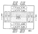
最初に本発明の表示装置の構成例について図1を用いて説明する。表示装置は、基板11上に形成された画素部Eを有し、さらに該画素部Eの周辺に配置されたデータドライバ(ここでは4つのデータドライバA〜D)及び走査ドライバ(8つの走査ドライバF1〜I1、F2〜I2)を有する。画面上半分の画素E−1はA、F1、F2、画面上半分の画素E−2はB、G1、G2により駆動される。同様に画面下半分の画素E−3はC、H1、H2、画面下半分の画素E−4はD、I1、I2により駆動される。
なお本形態では上下分割駆動を前提としているが、この上下分割駆動は本発明の実施に必須ではない。しかしながら、本発明と組み合わせることで、画素に対する映像信号の書き込み時間の確保はより効果的に行われる。
【0014】
データドライバA〜D及び走査ドライバF1〜I1、F2〜I2にはFPC12を介して外部より信号が供給される。なお上記ドライバは基板11上に形成してもよいし、別ICとして外部に配置してもよい。また上記ドライバの個数は特に限定されず、画素の構成等に応じて設定することができる。但し、データドライバの個数は、1列毎に配置されたデータ線の本数と同じであることが好ましい。またここでは画素部Eを4つの領域E−1〜E−4に大別したが、本発明はこれに限定されず、いくつの領域に大別してもよい。
【0015】
なお表示装置とは、発光素子を有する画素部及び駆動回路を基板とカバー材との間に封入したパネル、前記パネルにIC等を実装したモジュール、パソコンのモニターとして用いられるディスプレイなどを範疇に含む。つまり表示装置とは、パネル、モジュール及びディスプレイなどの総称に相当する。
【0016】
画素部Eの構成例についてここでは4つの形態について説明するが、まず第1の構成について図13(A)を用いて説明する。図13(A)において、画素部Eには複数の画素がマトリクス状に配置され、さらに各画素を列方向に2本のデータ線、各画素を行方向に1本の走査線が通っている。本形態では、画素部が中央で分割され、画面上半分にはデータ線SA、SBが配置され、画面下半分にはデータ線SC、SDが配置される。そして、データ線SAに接続した画素をE−1、データ線SBに接続した画素をE−2、データ線SCに接続した画素をE−3、データ線SDに接続した画素をE−4と表記する。つまり画素E−1はデータドライバA、画素E−2はデータドライバB、画素E−3はデータドライバC、画素E−4はデータドライバDにそれぞれ制御される。
【0017】
そして画面の左側には走査ドライバF1〜I1が配置され、画面の右側には走査ドライバF2〜I2が配置される。そして画素E−1の選択は、走査ドライバF1及びF2によって画面の左側及び右側の両方の方向から行われる。その他の画素E−2〜E−4も同様である。
なお走査ドライバは、必ずしも画面の両側に配置しなくてもよいが、画面の両側に配置することで、片側の場合に比べて画素の選択速度を向上させることができる。そのため、特に負荷が重くなる大画面の高解像度の表示装置では、走査ドライバは画面の両側に配置することが望ましい。
上記構成を有する本発明は、大型画面の表示装置に顕著である、配線に対する寄生容量が大きいために生ずる書き込み時間不足を解消することができる。
【0018】
ここで、画素部Eの画面上半分には(i×j)個の画素、画面下半分には(n×m)個の画素が配置されると仮定し、座標(i,j−1)、(i,j)、(n,m−1)、(n,m)に配置された4つの画素E−1〜E−4の構成について、図13(B)(C)を用いて説明する。なお画素の回路構成は自由に設計可能であるため、図中、画素内にはスイッチング用素子と発光素子のみを示す。
図13(B)(C)に示す4つの画素の各々は、異なるデータ線SA〜SDに制御される。そのため、画素E−1〜E−4を制御する4本の走査線G(j−1)〜Gj、G(m−1)〜Gmは同時に選択することが可能となり、その結果4つの画素には同じタイミングで信号を書き込むことが可能となる。そうすると、従来点順次駆動ならば1画素毎に信号を供給していたところをx個の画素に同時に信号を供給することが可能となり、さらに従来線順次駆動ならば1列目から最終列目(ここでは最終列はn列とおく)までのn個の画素に同時に信号を供給していたところを(x×n)個の画素に同時に信号を供給することが可能となる。本構成により、画素に対する書き込み時間を向上させることが可能となり、書き込み時間不足を解消することができる。
なお図13(C)は、隣接する画素間において、走査線を共通にした場合を示す。本発明は、1列に複数本の信号線を配置するため、開口率の向上のために、隣接する画素同士で走査線を共有してもよい。
【0019】
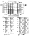
次いで第2の構成について、図2を用いて説明する。図2において、画素部Eには複数の画素がマトリクス状に配置され、さらに各画素を列方向に4本のデータ線、各画素を行方向に1本の走査線が通っている。そしてここでは、1列に配置された4本のデータ線をSA〜SDと表記し、上記の形態と同様に、データ線SAに接続した画素をE−1、データ線SBに接続した画素をE−2、データ線SCに接続した画素をE−3、データ線SDに接続した画素をE−4と表記する。
【0020】
次いで、座標(i.j)〜(i,j+3)に配置された4つの画素E−1〜E−4の構成例について、図2(B)(C)を用いて図示する。図2(B)(C)に示す4つの画素の各々は、異なるデータ線SA〜SDに制御される。そのため、画素E−1〜E−4は同時に選択することが可能となり、その結果4つの画素には同じタイミングで信号を書き込むことが可能となる。
【0021】
次いで第3の構成について、図8を用いて説明する。図8(A)において、画素部Eには複数の画素がマトリクス状に配置され、さらに各画素を列方向に2本のデータ線、各画素を行方向に1本の走査線が通っている。本形態では、画素部が中央で分割され、画面上半分にはデータ線SA,SB、画面下半分にはSC、SDが配置される。
そして、データドライバAに制御されるデータ線をSA、データドライバBに制御されるデータ線をSB、データドライバCに制御されるデータ線をSC、データドライバDに制御されるデータ線をSDと表記する。また上記第1、第2の形態と同様に、データ線SAに接続した画素をE−1、データ線SBに接続した画素をE−2、データ線SCに接続した画素をE−3、データ線SDに接続した画素をE−4と表記する。つまり画素E−1はデータドライバA、画素E−2はデータドライバB、画素E−3はデータドライバC、画素E−4はデータドライバDにそれぞれ制御される。
【0022】
ここで、画素E−1〜E−4の構成について、図8(B)(C)に示す。図8(B)(C)に示す4つの画素の各々は、異なるデータ線SA〜SDに制御される。そのため、画素E−1〜E−4は同時に選択することが可能となり、その結果4つの画素には同じタイミングで信号を書き込むことが可能となる。
【0023】
次いで第4の構成について、図14を用いて説明する。図14において、画素部Eには複数の画素がマトリクス状に配置され、さらに各画素を列方向に4本のデータ線、各画素を行方向に1本の走査線が通っている。そしてここでは、1列に配置された4本のデータ線をSA〜SDと表記し、上記の形態と同様に、データ線SAに接続した画素をE−1、データ線SBに接続した画素をE−2、データ線SCに接続した画素をE−3、データ線SDに接続した画素をE−4と表記する。つまり画素E−1はデータドライバA、画素E−2はデータドライバB、画素E−3はデータドライバC、画素E−4はデータドライバDにそれぞれ制御される。
【0024】
ここで、画素E−1からE−4の構成について、図14(B)(C)に示すE−1〜E−4の4つの画素の各々は、異なるデータ線SA〜SDに制御される。そのため、画素E−1〜E−4は同時に選択することが可能となり、その結果4つの画素には同じタイミングで信号を書き込むことが可能となる。
【0025】
次いで、上記の第1〜第4の構成の走査方法の例について、図9を用いて説明する。図8に示した第3の構成については図9(A)、図13に示した第1の構成については図9(B)、また図2、14に示した第2及び第4の構成については図9(C)を用いて説明する。
【0026】
図13に示した第1の構成では、画素部を1行目からm/2行目までと、(m/2+1)行目から最終行目(ここではm行とする)までの2つの領域に大別する。1行目から(m/2+1)行目に配置された画素のうち、奇数行目に配置された画素は走査ドライバF、偶数行目に配置された画素は走査ドライバGに制御される。(m/2+1)行目から最終行目に配置された画素のうち、奇数行目に配置された画素は走査ドライバH、偶数行目に配置された画素は走査ドライバIに制御される。そして、走査ドライバFにより1行目からm/2行目の方向に画素が走査され、同じタイミングで走査ドライバGによりm/4行目からm/2行目の方向に画素が走査される。
【0027】
図2、14に示した第2及び第4の構成では、複数の画素のうち、m行目、(m+1)行目、(m+2)行目、(m+3)行目に配置された画素に大別する。そして、m行目に配置された画素は走査ドライバF、(m+1)行目に配置された画素は走査ドライバG、(m+2)行目に配置された画素は走査ドライバH、(m+3)行目に配置された画素は走査ドライバIに制御される。
【0028】
図8に示した第3の構成では、画素部を1行目から最終行目(ここではm行とする)まで4つの領域に大別し、1行目からm/4行目に配置された画素は走査ドライバF、(m/4+1)行目からm/2行目までに配置された画素は走査ドライバG、(m/2+1)行目から(3×m)/4行目までに配置された画素は走査ドライバH、{(3×m)/4+1}行目から最終行目までに配置された画素は走査ドライバIに制御される。つまり、1行目からm/4行目に配置された画素が走査ドライバFにより走査され、同じタイミングで(m/4+1)行目からm/2行目に配置された画素が走査ドライバGにより走査される。m/2行目から(3×m)/4行目が走査ドライバHにより走査され、{(3×m)/4+1}行目から最終行目までに配置された画素が走査ドライバIにより走査される。
【0029】
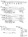
次いで、データドライバの構成例について説明する。ここではデータドライバAを例に挙げて、図3を用いて説明する。データドライバは複数の領域に大別し、各々を並行して動作させる。ここでは、A−1〜A−8の8個に大別されるとする。仮に画素数がカラーSXGAの場合には、A−1〜A−8の各々には(160×(RGB))本のデータ線が接続される。
そして、データドライバが点順次駆動を行う場合には、データドライバA−1〜A−8の各々はシフトレジスタSR1〜SR40とサンプリング回路SMP1〜SMP40を有する。またデータドライバが線順次駆動を行う場合には、データドライバA−1〜A−8の各々は、シフトレジスタSR1〜SR40及び第1ラッチL1−1〜L1−40、並びに第2ラッチL2−1〜L2−40を有する。仮に画素数がSXGAの場合には、SMP1〜SMP40の各々には(4×(RGB))本のデータ線が接続される。
【0030】
ここで、図3(B)のデータドライバの動作を簡単に説明する。このデータドライバは点順次駆動用で、映像信号が電圧形式のアナログ駆動の場合に適している。シフトレジスタSR1〜SR40の各々は、フリップフロップ回路(FF)やデコーダ等を複数列用いて構成され、クロック(S−CLK)やスタートパルス(S−SP)のタイミングに従って、順次サンプリングパルスを出力し、該サンプリングパルスをサンプリング回路SMP1〜SMP40に供給する。サンプリング回路SMP1〜SMP40にはビデオ信号が入力されており、入力されるサンプリングパルスのタイミングに従って、該サンプリング回路SMP1〜SMP40に入力されたビデオ信号はデータ線SA1〜SA160に出力される。
【0031】
次いで、図3(C)のデータドライバの動作を簡単に説明する。このデータドライバは線順次駆動用で、ディジタル時分割駆動の場合に適している。シフトレジスタは、上述したように順次サンプリングパルスを出力し、該サンプリングパルスはサンプリング回路SMP1〜SMP40(第1ラッチL1−1〜L1−40)に供給される。サンプリング回路SMP1〜SMP40には、ビデオ信号が入力されており、サンプリングパルスが入力されるタイミングに従って、各列でビデオ信号を保持していく。サンプリング回路SMP1〜SMP40において、最終列までビデオ信号の保持が完了すると、水平帰線期間中に、第2ラッチL2−1〜L2−40にラッチパルスが入力され、第1ラッチL1−1〜L1−40に保持されていたビデオ信号は、一斉に第2ラッチL2−1〜L2−40に転送される。そうすると、第2ラッチL2−1〜L2−40に保持されていたビデオ信号は、1行分がサンプリング回路SMP1〜SMP40を介して同時にデータ線SA1〜SA160に入力される。そして第2ラッチL2−1〜L2−40に保持されたビデオ信号がデータ線SA1〜SA160に入力されている間、シフトレジスタSR1〜SR40においては再びサンプリングパルスが出力される。以後この動作を繰り返す。
【0032】
ここで前記サンプリング回路SMP1〜SMP40のタイミングチャートを図3(C)に示す。図3(C)に示すように、SMP1〜SMP40の各々に配置された複数本のデータ線では、同時にビデオ信号の取り込みを行う。
【0033】
本実施形態のように、画素数SXGAで、15サブフレームの時分割駆動を表示する場合、データドライバのクロック周波数を5MHzとしたとき、1水平走査期間を4μsec以上とすることも可能となり、充分に実用可能である。
【0034】
次いで走査線ドライバの例について図3(E)を用いて説明する。この走査ドライバは、シフトレジスタ310、バッファ311を有する。動作を簡単に説明すると、シフトレジスタ310は、上述したように順次サンプリングパルスを出力する。その後バッファ311で増幅されたサンプリングパルスは、走査線に入力されて1行ずつ選択状態にしていく。そして選択された走査線によって制御される画素には、順にデータ線からビデオ信号が書き込まれる。なおシフトレジスタ310とバッファ311の間にはレベルシフタを配置した構成にしてもよい。レベルシフタを配置することによって、ロジック回路部とバッファ部の電圧振幅を変えることが出来る。
【0035】
上記構成を有する本発明は、表示装置の大型化及び高精細化に伴って生じる書き込み時間不足を解消した表示装置及びその駆動方法を提供する。特に本発明は、ディジタル時分割駆動やアナログ駆動で電流値形式の信号を用いる場合において顕著な書き込み時間不足を解消した表示装置及びその駆動方法を提供する。
【0036】
(実施の形態2)
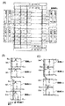
本実施の形態では、画素部Eのi列j行目に配置された画素について、代表的な構成例をいくつか挙げて、その構成を図4(A)(B)、図10(A)〜(D)を用いて説明する。図10(A)は、画素回路の一般的な表現をしたものであり、具体例としては、電圧形式の映像信号の場合は、図4(A)(B)など、電流形式の映像信号の場合は図10(B)〜(D)などが挙げられる。
【0037】
図4(A)(B)において、スイッチ用トランジスタ306のゲート電極は走査線Gjに接続され、第1のソース・ドレイン電極は信号線Siに接続され、第2のソース・ドレイン電極は駆動用トランジスタ307のゲート電極に接続されている。駆動用トランジスタ307の第1のソース・ドレイン電極は電源線Viに接続され、第2のソース・ドレイン電極は発光素子308の一方の電極に接続されている。発光素子308の他方の電極は電源線Cjに接続されている。
【0038】
また図4(B)において、スイッチ用トランジスタ306と消去用トランジスタ309とは直列に接続され、信号線Siと電源線Viの間に配置されている。消去用トランジスタ309のゲート電極は走査線Rjに接続されている。ここでは、駆動用トランジスタ307の第2のソース・ドレイン電極に接続された発光素子308の一方の電極を画素電極と呼び、電源線Cjに接続された他方の電極を対向電極と呼ぶ。
【0039】
図4(A)(B)において、スイッチ用トランジスタ306は、映像信号の画素への入力を制御する機能を有する。スイッチ用トランジスタ306はスイッチとしての機能を有していれば良いので、その導電型は特に限定されない。nチャネル型及びpチャネル型のいずれも用いることができる。
【0040】
また図4(A)(B)において、駆動用トランジスタ307は、発光素子308の発光を制御する機能を有する。駆動用トランジスタ307の導電型は特に限定されないが、駆動用トランジスタ307がpチャネル型であるとき、画素電極が陽極となり、対向電極が陰極となるのが好ましい。逆に駆動用トランジスタ307がnチャネル型であるとき、画素電極が陰極となり、対向電極が陽極となるのが好ましい。
【0041】
図4(B)において、消去用トランジスタ309は、発光素子308の発光を停止せしめる機能を有する。消去用トランジスタ309はスイッチとしての機能を有していれば良いので、その導電型は特に限定されない。
【0042】
上記図4(A)(B)に示した画素では、電圧の形式の信号が駆動用トランジスタ307のゲート電極に入力され、その駆動用トランジスタ307のドレイン電流が発光素子308に供給される。
【0043】
続いては、図10(A)に示すように、画素内に電流源312を配置し、該電流源312から所定の電流が発光素子308に供給される画素について説明する。前記電流源312は、信号線からビデオ信号が供給され、電源線から電流が供給され、制御線から制御信号が供給される。
【0044】
図10(B)において、トランジスタ313、314は、画素への信号の入力を制御する機能を有する。トランジスタ315のゲート・ソース間電圧は容量素子317によって所定の電圧に保持されているため、トランジスタ315は所定のドレイン電流を流す能力を有する。トランジスタ316は、発光素子308とトランジスタ315との導通を制御しており、トランジスタ316がオンであるとき、トランジスタ315のドレイン電流が発光素子308に供給される。図10(B)の回路は、画素へ入力した信号電流を、トランジスタ315を使って忠実に再現して、発光素子308に供給できる利点がある。但し、発光素子に供給する電流と、信号電流とを異なる値に出来ないのが難点である。
【0045】
図10(C)において、トランジスタ318は、画素への信号の入力を制御する機能を有する。トランジスタ319、320はカレントミラー回路を構成し、トランジスタ319、320のゲート・ソース間電圧は容量素子322によって所定の電圧に保持されているため、トランジスタ319、320は所定のドレイン電流を流す能力を有する。トランジスタ321は、トランジスタ320のゲートとトランジスタ319のドレインの間に配置される。図10(C)の回路は、トランジスタ319と320とのサイズ比を変化させることにより、発光素子308に供給する電流と信号電流との比を自由に設定できるのが利点である。しかし、トランジスタ319と320の特性が等しくないと、トランジスタ320により発光素子308に供給される電流が、画素毎に変わってしまい、表示ムラとして視認されてしまう難点がある。
【0046】
図10(D)において、トランジスタ71〜75は、画素への信号の入力を制御する機能を有する。画素へ信号を書き込むときには、トランジスタ71〜78をオンにして、トランジスタ79、85をオフにする。逆に発光素子308に電流を供給するときには、トランジスタ71〜78をオフにして、トランジスタ79、85をオンにする。図10(D)の回路は、図10(B)(C)の回路の双方の利点を持つ。
【0047】
画素に配置されるトランジスタは、ゲート電極が1本のシングルゲート構造だけではなく、ゲート電極が2本のダブルゲート構造やゲート電極が3本のトリプルゲート構造などのマルチゲート構造を有していてもよい。またゲート電極が半導体の上部に配置されたトップゲート構造、ゲート電極が半導体の下部に配置されたボトムゲート構造のいずれの構造を有していてもよい。また図4(A)(B)に示す画素は、トランジスタ307のソース・ゲート間の容量結合が大きいことを前提に、容量素子を明示していないが、本発明はこれに限定されずトランジスタ307のゲート・ソース間電圧を保持する容量素子を配置してもよい。また発光素子308とは、陽極及び陰極、並びに前記陽極と前記陰極との間に発光層が挟まれた構造を有する。前記発光層は、有機材料、カーボンナノライトなどの無機材料及びバルク材料などから選択された1つ又は複数の材料により構成される。
【0048】
なお隣接した画素同士で電源線Viを共有してもよい。つまり、必ずしも1列単位で電源線を設ける必要はなく、隣接する列同士で同一の電源線を共有することが出来る。本発明は、1列に複数本の信号線を配置するため、隣接する列同士で電源線を共有することは、開口率の向上に役立つ。
【0049】
但し、カラー表示を行う表示装置においては、1画素に配置されたRGBの各色に対応した各画素は、RGBの各材料の電流密度やカラーフィルタなどの透過率の相違により、同じ電圧を印加しても発せられる光の輝度は異なってしまうことがある。そのため、この場合には各色に対応した電源線を配置し、各色で電位を設定するようにしてもよい。なお本発明では、RGB1組を1画素と称するのではなく、Rだけで1画素、Gだけで1画素、Bだけで1画素と称することにする。
【0050】
次いで、本発明の表示装置に時分割駆動を適用したときの動作について図4(C)〜(E)を用いて説明する。図4(C)〜(E)に示したタイミングチャートは、横軸は時間を示し、縦軸は走査線を示す。
【0051】
時分割駆動では、1フレーム期間は複数のサブフレーム期間SFに分割される。各サブフレーム期間SFは、書き込み期間Ta及び表示期間Ts、又は書き込み期間Ta及び表示期間Ts並びに消去期間Teを有する。
【0052】
消去期間Teは、書き込み期間Taよりも短い表示期間Tsを有するサブフレーム期間SFにのみ設けられる。これは表示期間Tsの終了後、直ちに次の書き込み期間Taが開始しないようにするためである。仮に表示期間Tsの終了後、直ちに書き込み期間Taが開始されると、同じタイミングで走査線を2本選択することになって、信号線から画素に正しい信号を入力できなくなるからである。
【0053】
時分割駆動では、各サブフレーム期間SFにおける発光期間の長さを異なるものとし、各サブフレーム期間SFの点灯又は非点灯の組み合わせにより階調を表現する。図4に示した例では、階調数を5ビットとして、1フレーム期間を5つのサブフレーム期間SF1〜SF5に分割している。そして各サブフレーム期間が有する表示期間Ts1〜Ts5の長さをTs1:Ts2:Ts3:Ts4:Ts5=16:8:4:2:1というように2のべき乗として、多階調が得られるようにしている。つまり、nビット階調を表現するときは、表示期間Ts1〜Tsnの長さの比は、2(n−1):2(n−2):・・・:21:20となる。そして書き込み期間Taは、各画素にディジタルビデオ信号を書き込む期間であり、各サブフレーム期間SFでの長さは等しい。表示期間Tsは、各画素に書き込まれたビデオ信号に基づいて、画素が点灯又は非点灯を行う期間である。
【0054】
ここで、図4(B)の画素を例に挙げて、上記の書き込み期間Ta及び表示期間Ts並びに消去期間Teの各期間における動作について説明する。
【0055】
まず書き込み期間Taにおいて、走査線Gjはパルスが入力されてHレベルとなり、スイッチ用トランジスタ306はオンする。そうすると、信号線Siに出力されたディジタルビデオ信号が駆動用トランジスタ307のゲート電極に入力される。
次いで、表示期間Tsにおいて、駆動用トランジスタ307がオンすることによって、電源線Viの電位と電源線Cjとの電位差によって発光素子308に電流が流れて発光する。また駆動用トランジスタ307がオフのときは、発光素子308に電流は流れず、非発光となる。
続いて、消去期間Teにおいて、走査線Rjはパルスが入力されてHレベルとなり、消去用トランジスタ309がオンする。消去用トランジスタ309がオンすると、駆動用トランジスタ307のゲート・ソース間電圧がゼロとなり、駆動用トランジスタ307はオフする。そうすると、発光素子308には電流が供給されなくなり、非発光の状態となる。なお消去期間Teは、サブフレーム期間SF5のみ設けられている。これはサブフレーム期間SF5においては、書き込み期間Ta5よりも短い表示期間Ts5を有しているため、該表示期間Ts5の終了後、直ちに次の書き込み期間が開始しないようにするためである。
【0056】
図4のタイミングチャートでは、サブフレーム期間SF1〜SF5が順に出現していたが、本発明はこれに限定されない。サブフレーム期間はランダムに出現してもよい。また擬似輪郭等の表示妨害を抑制するため、任意のサブフレーム期間を分割して出現させてもよい。
【0057】
上記構成を有する本発明は、表示装置の大型化及び高精細化に伴って生じる書き込み時間不足を解消した表示装置及びその駆動方法を提供する。特に本発明は、ディジタル時分割駆動やアナログ駆動で電流値形式の信号を用いる場合において顕著な書き込み時間不足を解消した表示装置及びその駆動方法を提供する。
【0058】
本実施の形態は、実施の形態1と任意に組み合わせることが可能である。
【0059】
(実施の形態3)
本実施の形態では、図2に示した形態に図4(A)に示した回路を適用した場合における、画素のレイアウト上面図について図5を用いて説明する。
【0060】
図5には画素E−1〜E−4の4つの画素を図示し、列方向にデータ線SAi〜SDi、行方向に走査線Gj〜G(j+3)が配置されている。各画素は、スイッチ用TFT、駆動用TFT及び容量体を有する。駆動用TFTに接続される発光素子は、画素電極及び発光層並びに対向電極の積層体に相当するが、図5では画素電極のみを図示している。
【0061】
スイッチ用TFTはダブルゲート型トランジスタとしているが、本発明はこれに限定されず、シングルゲート型であっても、任意の数のマルチゲート型であっても良い。また図中、駆動用TFTのゲート・ソース間電圧を保持するための手段として、電源線及びゲート電極と同じ層で形成された金属体並びにその間に配置された絶縁体で容量体を形成している。しかしながら、駆動用TFT自身のゲート容量及びチャネル容量、配線等の寄生容量で、駆動用TFTのゲート・ソース間電圧を保持することが可能な場合には、新たに容量体を配置しなくてもよい。
【0062】
本実施の形態は、実施の形態1、2と任意に組み合わせることが可能である。
【0063】
(実施の形態4)
本発明が適用される電子機器として、ビデオカメラ、ディジタルカメラ、ゴーグル型ディスプレイ(ヘッドマウントディスプレイ)、ナビゲーションシステム、音響再生装置(カーオーディオ、オーディオコンポ等)、ノート型パーソナルコンピュータ、ゲーム機器、携帯情報端末(モバイルコンピュータ、携帯電話、携帯型ゲーム機または電子書籍等)、記録媒体を備えた画像再生装置(具体的にはDigital Versatile Disc(DVD)等の記録媒体を再生し、その画像を表示しうるディスプレイを備えた装置)などが挙げられる。それらの電子機器の具体例を図6に示す。
【0064】
図6(A)は発光装置であり、筐体2001、支持台2002、表示部2003、スピーカー部2004、ビデオ入力端子2005等を含む。本発明は表示部2003に適用することができる。また本発明により、図6(A)に示す発光装置が完成される。発光装置は自発光型であるためバックライトが必要なく、液晶ディスプレイよりも薄い表示部とすることができる。なお、発光装置は、パソコン用、TV放送受信用、広告表示用などの全ての情報表示用表示装置が含まれる。
【0065】
図6(B)はディジタルスチルカメラであり、本体2101、表示部2102、受像部2103、操作キー2104、外部接続ポート2105、シャッター2106等を含む。本発明は、表示部2102に適用することができる。また本発明により、図6(B)に示すディジタルスチルカメラが完成される。
【0066】
図6(C)はノート型パーソナルコンピュータであり、本体2201、筐体2202、表示部2203、キーボード2204、外部接続ポート2205、ポインティングマウス2206等を含む。本発明は、表示部2203に適用することができる。また本発明により、図6(C)に示す発光装置が完成される。
【0067】
図6(D)はモバイルコンピュータであり、本体2301、表示部2302、スイッチ2303、操作キー2304、赤外線ポート2305等を含む。本発明は、表示部2302に適用することができる。また本発明により、図6(D)に示すモバイルコンピュータが完成される。
【0068】
図6(E)は記録媒体を備えた携帯型の画像再生装置(具体的にはDVD再生装置)であり、本体2401、筐体2402、表示部A2403、表示部B2404、記録媒体(DVD等)読み込み部2405、操作キー2406、スピーカー部2407等を含む。表示部A2403は主として画像情報を表示し、表示部B2404は主として文字情報を表示するが、本発明は表示部A、B2403、2404に適用することができる。なお、記録媒体を備えた画像再生装置には家庭用ゲーム機器なども含まれる。また本発明により図6(E)に示す画像表示装置が完成される。
【0069】
図6(F)はゴーグル型ディスプレイ(ヘッドマウントディスプレイ)であり、本体2501、表示部2502、アーム部2503を含む。本発明は、表示部2502に適用することができる。また本発明により、図6(F)に示すゴーグル型ディスプレイが完成される。
【0070】
図6(G)はビデオカメラであり、本体2601、表示部2602、筐体2603、外部接続ポート2604、リモコン受信部2605、受像部2606、バッテリー2607、音声入力部2608、操作キー2609等を含む。本発明は、表示部2602に適用することができる。また本発明により、図6(G)に示すビデオカメラが完成される。
【0071】
図6(H)は携帯電話であり、本体2701、筐体2702、表示部2703、音声入力部2704、音声出力部2705、操作キー2706、外部接続ポート2707、アンテナ2708等を含む。本発明は、表示部2703に適用することができる。なお、表示部2703は黒色の背景に白色の文字を表示することで携帯電話の消費電流を抑えることができる。また本発明により、図6(H)に示す携帯電話が完成される。
【0072】
なお、将来的に発光材料の進歩により高輝度発光使用が可能となれば、出力した画像情報を含む光をレンズ等で拡大投影してフロント型若しくはリア型のプロジェクターに用いることも可能となる。
【0073】
また、上記電子機器はインターネットやCATV(ケーブルテレビ)などの電子通信回線を通じて配信された情報を表示することが多くなり、特に動画情報を表示する機会が増してきている。発光材料の応答速度は非常に高いため、発光装置は動画表示に好ましい。
【0074】
また、発光装置は発光している部分が電力を消費するため、発光部分が極力少なくなるように情報を表示することが望ましい。従って、携帯情報端末、特に携帯電話や音響再生装置のような文字情報を主とする表示部に発光装置を用いる場合には、非発光部分を背景として文字情報を発光部分で形成するように駆動することが望ましい。
【0075】
以上の様に、本発明の適用範囲は極めて広く、あらゆる分野の電子機器に用いることが可能である。また本実施の形態の電子機器は、実施の形態1〜3に示したいずれの構成の表示装置を用いても良い。
【0076】
(実施の形態5)
形態4において示した電子機器には、発光素子が封止された状態にあるパネルに、コントローラ、電源回路等を含むICが実装された状態にあるモジュールが搭載されている。モジュールとパネルは、共に表示装置の一形態に相当する。ここでは、モジュールの具体的な構成例について説明する。
【0077】
図11(A)に、コントローラ801及び電源回路802がパネル800に実装されたモジュールの外観図を示す。パネル800には、発光素子が各画素に設けられた画素部803と、前記画素部803が有する画素を選択する走査線駆動回路804と、選択された画素にビデオ信号を供給する信号線駆動回路805とが設けられている。
【0078】
またプリント基板806にはコントローラ801、電源回路802が設けられており、コントローラ801または電源回路802から出力された各種信号及び電源電圧は、FPC807を介してパネル800の画素部803、走査線駆動回路804、信号線駆動回路805に供給される。
【0079】
プリント基板806への電源電圧及び各種信号は、複数の入力端子が配置されたインターフェース(I/F)部808を介して供給される。
【0080】
なお、本実施例ではパネル800にプリント基板806がFPCを用いて実装されているが、必ずしもこの構成に限定されない。COG(Chip on Glass)方式を用い、コントローラ801、電源回路802をパネル800に直接実装させるようにしても良い。
【0081】
また、プリント基板806において、引きまわしの配線間に形成される容量や配線自体が有する抵抗等によって、電源電圧や信号にノイズがのったり、信号の立ち上がりが鈍ったりすることがある。そこで、プリント基板806にコンデンサ、バッファ等の各種素子を設けて、電源電圧や信号にノイズがのったり、信号の立ち上がりが鈍ったりするのを防ぐようにしても良い。
【0082】
図11(B)に、プリント基板806の構成をブロック図で示す。インターフェース808に供給された各種信号と電源電圧は、コントローラ801と、電源電圧802に供給される。
【0083】
コントローラ801は、アナログインターフェイス回路809と、位相ロックドループ(PLL:Phase Locked Loop)810と、制御信号生成部811と、SRAM(Static Random Access Memory)812、813とを有している。なお本実施例ではSRAMを用いているが、SRAMの代わりに、SDRAMや、高速でデータの書き込みや読み出しが可能であるならばDRAM(Dynamic Random
Access Memory)も用いることが可能である。
【0084】
インターフェース808を介して供給されたアナログビデオ信号は、アナログインターフェイス回路809においてAD変換及びパラレル−シリアル変換され、R、G、Bの各色に対応するディジタルビデオ信号として制御信号生成部811に入力される。また、インターフェース808を介して供給された各種信号をもとに、アナログインターフェイス回路809においてHsync信号、Vsync信号、クロック信号CLKなどが生成され、制御信号生成回路811に入力される。但し、インターフェース808に直接ディジタルビデオ信号が入力されるときは、アナログインターフェイス回路809は配置しなくてもよい。
【0085】
位相ロックドループ810では、インターフェース808を介して供給される各種信号の周波数と、制御信号生成回路811の動作周波数の位相とを合わせる機能を有している。制御信号生成回路811の動作周波数は、インターフェース808を介して供給された各種信号の周波数と必ずしも同じではないが、互いに同期するように制御信号生成回路811の動作周波数を位相ロックドループ810において調整する。
【0086】
制御信号生成回路811に入力されたビデオ信号は、一旦SRAM812、813に書き込まれ、保持される。制御信号生成回路811では、SRAM812に保持されている全ビットのビデオ信号のうち、全画素に対応するビデオ信号を1ビット分づつ読み出し、パネル800の信号線駆動回路805に供給する。
【0087】
また制御信号生成回路811では、各ビットの発光素子が発光する期間に関する情報を、パネル800の走査線駆動回路804に供給する。
【0088】
また電源回路802は所定の電源電圧を、パネル800の信号線駆動回路805、走査線駆動回路804及び画素部803に供給する。
【0089】
次に電源回路802の詳しい構成について、図12を用いて説明する。電源回路802は、4つのスイッチングレギュレータコントロール860を用いたスイッチングレギュレータ854と、シリーズレギュレータ855とからなる。
【0090】
一般的にスイッチングレギュレータは、シリーズレギュレータに比べて小型、軽量であり、降圧だけでなく昇圧や正負反転することも可能である。一方シリーズレギュレータは、降圧のみに用いられるが、スイッチングレギュレータに比べて出力電圧の精度は良く、リプルやノイズはほとんど発生しない。本実施例の電源回路802では、両者を組み合わせて用いる。
【0091】
図12に示すスイッチングレギュレータ854は、スイッチングレギュレータコントロール(SWR)860と、アテニュエイター(減衰器:ATT)861と、トランス(T)862と、インダクター(L)863と、基準電源(Vref)864と、発振回路(OSC)865、ダイオード866と、バイポーラトランジスタ867と、可変抵抗868と、容量869とを有している。
【0092】
スイッチングレギュレータ854において外部のLiイオン電池(3.6V)等の電圧が変換されることで、陰極に与えられる電源電圧と、スイッチングレギュレータ854に供給される電源電圧が生成される。
【0093】
またシリーズレギュレータ855は、バンドギャップ回路(BG)870と、アンプ871と、オペアンプ872と、電流源873と、可変抵抗874と、バイポーラトランジスタ875とを有し、スイッチングレギュレータ854において生成された電源電圧が供給されている。
【0094】
シリーズレギュレータ855では、スイッチングレギュレータ854において生成された電源電圧を用い、バンドギャップ回路870において生成された一定の電圧に基づいて、各色の発光素子の陽極に電流を供給するための配線(電流供給線)に与える直流の電源電圧を、生成する。
【0095】
なお電流源873は、ビデオ信号の電流が画素に書き込まれる駆動方式の場合に用いる。この場合、電流源873において生成された電流は、パネル800の信号線駆動回路805に供給される。なお、ビデオ信号の電圧が画素に書き込まれる駆動方式の場合には、電流源873は必ずしも設ける必要はない。
【0096】
【発明の効果】
本発明は、1列毎にx本のデータ線(xは4以上の自然数)を配置し、該x本のデータ線の各々を介してx個の画素に信号を同時に供給することが可能な表示装置及びその駆動方法を提供する。さらに本発明は、データ線を選択するデータドライバを複数配置することで、従来点順次駆動では1画素毎に信号を供給していたところをx個の画素に同時に信号を供給することを可能とし、さらに従来線順次駆動では1列目から最終列目(ここでは最終列はn列とおく)までのn個の画素に信号を供給していたところを(x×n)個の画素に同時に信号を供給することを可能とした表示装置およびその駆動方法を提供する。
【0097】
上記構成を有する本発明は、表示装置の大型化及び高精細化に伴って生じる書き込み時間不足を解消した表示装置及びその駆動方法を提供する。特に本発明は、ディジタル時分割駆動やアナログ駆動で電流値形式の信号を用いる場合において顕著な書き込み時間不足を解消した表示装置及びその駆動方法を提供する。
【図面の簡単な説明】
【図1】表示装置を示す図。
【図2】画素部及び画素の回路図。
【図3】データドライバを示す図。
【図4】画素の回路図及び駆動方法を説明するタイミングチャート。
【図5】画素のマスクレイアウト図。
【図6】本発明が適用される電子機器の図。
【図7】画素部の回路図。
【図8】画素部の回路図。
【図9】駆動方法を説明する図。
【図10】画素の回路図。
【図11】モジュールの図。
【図12】電源回路の図。
【図13】画素部及び画素の回路図。
【図14】画素部及び画素の回路図。[0001]
TECHNICAL FIELD OF THE INVENTION
The present invention relates to a display device using a light emitting element, and particularly to the technical field of a large-sized and high-resolution display device.
[0002]
[Prior art]
In recent years, the importance of display devices for displaying images has been increasing more and more. At present, as a display device, a liquid crystal display device which displays an image using a liquid crystal element is widely used taking advantage of high image quality, thinness, light weight, and the like. As other display devices, a display device (light-emitting device) using a light-emitting element such as an organic light-emitting diode (OLED) has been developed. A light-emitting device using an OLED (OLED display device) has attracted much attention because it has features such as a high response speed, excellent moving image display, and a wide field of view, in addition to the above advantages of the existing liquid crystal display device. . OLEDs, which are typical light-emitting elements used in light-emitting devices, have a structure having a single-layer or laminated thin film between a conductive anode and a cathode. Organic materials are included. Generally, the luminance of an organic light emitting diode and its current value satisfy a proportional relationship.
[0003]
Hereinafter, the light-emitting device has a plurality of pixels each including a light-emitting element (eg, an OLED) and at least two transistors in a matrix. In the pixel, a transistor connected in series to the light-emitting element and controlling the luminance of the light-emitting element is referred to as a driving transistor. A voltage or current type video signal is used for controlling the pixel. When a voltage type signal is used, a signal voltage is usually input to the gate electrode of the driving transistor, and light emission is performed using the driving transistor. Controls the brightness of the device. When a current-type signal is used, the luminance of the light-emitting element is controlled by supplying a current corresponding to a predetermined signal current from the driving transistor to the light-emitting element. Regardless of whether the video signal is in the voltage format or the current format, there are a case where an analog value signal is used (hereinafter referred to as analog driving) and a case where a digital value signal is used (hereinafter referred to as digital driving). In the case of digital driving, time division driving (for example, Japanese Patent Application Laid-Open No. 2001-5426) that expresses an intermediate gray scale in the form of a time ratio or area gray scale drive (for example, Japanese Patent Application No. 2001-382530) that expresses an intermediate gray scale in the form of an area ratio No.). Since the response speed of the OLED is higher than that of a liquid crystal or the like, the OLED is suitable for digital drive time division driving.
[0004]
Here, FIG. 7 schematically shows a pixel portion and a driving circuit of a conventional display device which performs matrix display. The pixel portion includes a plurality of scanning lines arranged in a row direction in which horizontal scanning is performed, a plurality of data lines arranged in a column direction orthogonal to the rows, and a plurality of pixels arranged in a matrix. As described above, a plurality of pixels are regularly arranged in the pixel portion, and one scanning line is arranged for each row and one data line is arranged for each column.
[0005]
[Problems to be solved by the invention]
If the frame frequency is constant, one horizontal scanning period becomes shorter as the resolution of the pixel portion increases. For example, if the frame frequency is 60 Hz and the number of pixels is SXGA standard (1280 × 1024), one horizontal scanning period is 16 μsec. About. In such a case, it is not easy to secure the time for writing the video signal to the pixel. In particular, in the case of a display device with a large screen in which the parasitic capacitance to the wiring is large, this tendency is remarkable.
[0006]
Let's consider a specific case. First, the case of digital time division gray scale is considered regardless of whether the video signal is in a current value format or a voltage value format. For example, when one frame is divided into about 15 sub-frames and time-division driving is performed, one horizontal scanning period is typically 1 μsec. When the number of pixels is SXGA standard (1280 × 1024). Below, the writing time is insufficient.
Next, a case of analog driving using a video signal in a current value format will be considered. When displaying a low-brightness gradation in which the video signal current supplied to the light emitting element is small, the writing speed becomes extremely slow, and the writing time is actually short.
[0007]
The present invention has been made in view of the above-described problems, and it is an object of the present invention to provide a display device and a method for driving the display device in which writing time shortage caused by an increase in size and resolution of the display device is eliminated. In particular, it is an object of the present invention to provide a display device and a driving method thereof in which a remarkable shortage of writing time is solved when a video signal of a current value format is used in digital time division driving or analog driving.
[0008]
[Means for Solving the Problems]
In order to solve the above-mentioned problem, the present invention arranges x data lines (x is a natural number of 4 or more) for each column, and applies x pixels to x pixels via each of the x data lines. Provided is a display device capable of simultaneously supplying signals and a driving method thereof. The present invention makes it possible to simultaneously supply a video signal to x pixels instead of supplying a signal for each pixel in the conventional point-sequential driving. A display device capable of supplying a video signal to (x × n) pixels at the same time where a signal is supplied to n pixels up to (here, the last column is assumed to be n columns) and the display device A driving method is provided. As a result, in the present invention, it is possible to make the writing time of the video signal to the pixel x times as long as the conventional one.
[0009]
According to the present invention, a plurality of data lines in a column direction, a plurality of scanning lines in a row direction, and a plurality of pixels each having a light emitting element (typically, an organic light emitting diode, OLED) are arranged in a matrix. A display device,
X data lines (x is a natural number of 4 or more) are arranged for each column of the plurality of data lines.
[0010]
The present invention is also applicable to a case where a data driver is arranged on each of the upper and lower sides and a video signal is written by operating the upper half pixel of the screen and the lower half pixel of the screen independently (hereinafter referred to as upper and lower division driving). Can be. In this case, when combined vertically, the number of data lines per column can be (2 × x) (x is a natural number of 2 or more).
[0011]
The present invention having the above structure provides a display device in which writing time shortage caused by an increase in size and definition of a display device is eliminated, and a driving method thereof. In particular, the present invention provides a display device and a method of driving the display device in which remarkable shortage of writing time is eliminated when a signal of a current value format is used in digital time division driving or analog driving.
[0012]
BEST MODE FOR CARRYING OUT THE INVENTION
(Embodiment 1)
The present invention will be described with reference to FIGS. 1 to 3, 8, 9, 13 and 14.
[0013]
First, a configuration example of a display device of the present invention will be described with reference to FIG. The display device has a pixel portion E formed on the
Although the present embodiment is based on the assumption that the upper and lower division driving is performed, the upper and lower division driving is not essential for implementing the present invention. However, in combination with the present invention, the time for writing the video signal to the pixel can be more effectively secured.
[0014]
Signals are externally supplied to the data drivers A to D and the scan drivers F1 to I1 and F2 to I2 via the
[0015]
Note that a display device includes a panel in which a pixel portion having a light-emitting element and a driver circuit are sealed between a substrate and a cover material, a module in which an IC or the like is mounted on the panel, a display used as a monitor of a personal computer, and the like. . That is, the display device corresponds to a general term for a panel, a module, a display, and the like.
[0016]
Four examples of the configuration example of the pixel portion E will be described here. First, the first configuration will be described with reference to FIG. In FIG. 13A, a plurality of pixels are arranged in a matrix in a pixel portion E, and each pixel is passed by two data lines in a column direction and each pixel is passed by one scanning line in a row direction. . In this embodiment, the pixel portion is divided at the center, data lines SA and SB are arranged in the upper half of the screen, and data lines SC and SD are arranged in the lower half of the screen. The pixel connected to the data line SA is E-1, the pixel connected to the data line SB is E-2, the pixel connected to the data line SC is E-3, and the pixel connected to the data line SD is E-4. write. That is, the pixel E-1 is controlled by the data driver A, the pixel E-2 is controlled by the data driver B, the pixel E-3 is controlled by the data driver C, and the pixel E-4 is controlled by the data driver D.
[0017]
Scan drivers F1 and I1 are arranged on the left side of the screen, and scan drivers F2 and I2 are arranged on the right side of the screen. The selection of the pixel E-1 is performed by the scanning drivers F1 and F2 from both the left and right sides of the screen. The same applies to the other pixels E-2 to E-4.
Note that the scanning drivers need not necessarily be arranged on both sides of the screen, but by arranging them on both sides of the screen, the selection speed of pixels can be improved as compared with the case of one side. Therefore, it is desirable to arrange the scanning drivers on both sides of the screen, particularly in a large-screen high-resolution display device where the load becomes heavy.
The present invention having the above structure can solve a shortage of writing time caused by a large parasitic capacitance to a wiring, which is remarkable in a display device with a large screen.
[0018]
Here, it is assumed that (i × j) pixels are arranged in the upper half of the screen of the pixel unit E and (n × m) pixels are arranged in the lower half of the screen, and coordinates (i, j−1) , (I, j), (n, m-1), and (n, m), the configuration of four pixels E-1 to E-4 will be described with reference to FIGS. I do. Note that since the circuit configuration of the pixel can be freely designed, only the switching element and the light emitting element are shown in the pixel in the drawing.
Each of the four pixels shown in FIGS. 13B and 13C is controlled by different data lines SA to SD. Therefore, four scanning lines G for controlling the pixels E-1 to E-4 are used. (J-1) ~ G j , G (M-1) ~ G m Can be simultaneously selected, and as a result, signals can be written to the four pixels at the same timing. This makes it possible to simultaneously supply signals to x pixels, instead of supplying signals for each pixel in the case of the conventional dot sequential driving, and further, in the case of the conventional line sequential driving, from the first column to the last column ( Here, it is possible to simultaneously supply signals to (x × n) pixels, instead of supplying signals to n pixels up to the n-th column at the same time. With this configuration, the writing time for the pixel can be improved, and the shortage of the writing time can be solved.
Note that FIG. 13C illustrates a case where the scanning line is shared between adjacent pixels. In the present invention, since a plurality of signal lines are arranged in one column, adjacent pixels may share a scanning line in order to improve an aperture ratio.
[0019]
Next, the second configuration will be described with reference to FIG. In FIG. 2, a plurality of pixels are arranged in a matrix in a pixel section E, and each pixel passes through four data lines in a column direction and each pixel passes through one scanning line in a row direction. Here, the four data lines arranged in one column are denoted by SA to SD, and the pixel connected to the data line SA is E-1 and the pixel connected to the data line SB is the same as in the above embodiment. E-2, the pixel connected to the data line SC is denoted as E-3, and the pixel connected to the data line SD is denoted as E-4.
[0020]
Next, a configuration example of four pixels E-1 to E-4 arranged at coordinates (ij) to (i, j + 3) will be illustrated with reference to FIGS. Each of the four pixels shown in FIGS. 2B and 2C is controlled by different data lines SA to SD. Therefore, the pixels E-1 to E-4 can be simultaneously selected, and as a result, signals can be written to the four pixels at the same timing.
[0021]
Next, a third configuration will be described with reference to FIG. In FIG. 8A, a plurality of pixels are arranged in a matrix in a pixel portion E, and each pixel passes two data lines in a column direction, and each pixel passes one scanning line in a row direction. . In this embodiment, the pixel portion is divided at the center, and data lines SA and SB are arranged in the upper half of the screen, and SC and SD are arranged in the lower half of the screen.
The data line controlled by the data driver A is denoted by SA, the data line controlled by the data driver B is denoted by SB, the data line controlled by the data driver C is denoted by SC, and the data line controlled by the data driver D is denoted by SD. write. Similarly to the first and second embodiments, the pixel connected to the data line SA is E-1, the pixel connected to the data line SB is E-2, the pixel connected to the data line SC is E-3, The pixel connected to the line SD is denoted by E-4. That is, the pixel E-1 is controlled by the data driver A, the pixel E-2 is controlled by the data driver B, the pixel E-3 is controlled by the data driver C, and the pixel E-4 is controlled by the data driver D.
[0022]
Here, the configurations of the pixels E-1 to E-4 are shown in FIGS. Each of the four pixels shown in FIGS. 8B and 8C is controlled by different data lines SA to SD. Therefore, the pixels E-1 to E-4 can be simultaneously selected, and as a result, signals can be written to the four pixels at the same timing.
[0023]
Next, a fourth configuration will be described with reference to FIG. In FIG. 14, a plurality of pixels are arranged in a matrix in a pixel portion E, and each pixel passes through four data lines in a column direction and each pixel passes through one scanning line in a row direction. Here, the four data lines arranged in one column are denoted by SA to SD, and the pixel connected to the data line SA is E-1 and the pixel connected to the data line SB is the same as in the above embodiment. E-2, the pixel connected to the data line SC is denoted as E-3, and the pixel connected to the data line SD is denoted as E-4. That is, the pixel E-1 is controlled by the data driver A, the pixel E-2 is controlled by the data driver B, the pixel E-3 is controlled by the data driver C, and the pixel E-4 is controlled by the data driver D.
[0024]
Here, regarding the configuration of the pixels E-1 to E-4, each of the four pixels E-1 to E-4 shown in FIGS. 14B and 14C is controlled by a different data line SA to SD. . Therefore, the pixels E-1 to E-4 can be simultaneously selected, and as a result, signals can be written to the four pixels at the same timing.
[0025]
Next, an example of the above-described first to fourth configuration scanning methods will be described with reference to FIG. 9A for the third configuration shown in FIG. 8, FIG. 9B for the first configuration shown in FIG. 13, and the second and fourth configurations shown in FIGS. Will be described with reference to FIG.
[0026]
In the first configuration shown in FIG. 13, the pixel portion has two regions from the first line to the m / 2th line and from the (m / 2 + 1) th line to the last line (here, m-th line). Roughly divided into Of the pixels arranged in the first to (m / 2 + 1) th rows, the pixels arranged in the odd rows are controlled by the scanning driver F, and the pixels arranged in the even rows are controlled by the scanning driver G. Of the pixels arranged from the (m / 2 + 1) th row to the last row, the pixels arranged on the odd rows are controlled by the scan driver H, and the pixels arranged on the even rows are controlled by the scan driver I. The scanning driver F scans pixels in the direction from the first row to the m / 2-th row, and the scanning driver G scans pixels in the direction from the m / 4-th row to the m / 2-th row at the same timing.
[0027]
In the second and fourth configurations shown in FIGS. 2 and 14, among the plurality of pixels, the pixels arranged in the m-th row, the (m + 1) -th row, the (m + 2) -th row, and the (m + 3) -th row are large. Separate. The pixel arranged on the m-th row is the scanning driver F, the pixel arranged on the (m + 1) -th row is the scanning driver G, the pixel arranged on the (m + 2) -th row is the scanning driver H, and the (m + 3) -th row. Are controlled by the scanning driver I.
[0028]
In the third configuration shown in FIG. 8, the pixel portion is roughly divided into four regions from the first row to the last row (here, m rows), and is arranged from the first row to the m / 4th row. The pixels arranged in the scanning driver F, the pixels arranged in the (m / 4 + 1) th row to the m / 2th row are the scanning driver G, and the pixels arranged in the (m / 2 + 1) th row to the (3 × m) / 4th row. The arranged pixels are controlled by the scanning driver H, and the pixels arranged from the {(3 × m) / 4 + 1} row to the last row are controlled by the scanning driver I. That is, the pixels arranged from the first row to the m / 4th row are scanned by the scan driver F, and the pixels arranged from the (m / 4 + 1) th row to the m / 2th row are scanned by the scan driver G at the same timing. Scanned. The scan driver H scans the m / 2th to (3 × m) / 4 rows, and the scan driver I scans the pixels arranged from the {(3 × m) / 4 + 1} row to the last row. Is done.
[0029]
Next, a configuration example of the data driver will be described. Here, the data driver A will be described as an example with reference to FIG. The data driver is roughly divided into a plurality of areas, and each operates in parallel. Here, it is assumed that the data is roughly divided into eight, A-1 to A-8. If the number of pixels is color SXGA, (160 × (RGB)) data lines are connected to each of A-1 to A-8.
When the data driver performs the dot sequential driving, each of the data drivers A-1 to A-8 has shift registers SR1 to SR40 and sampling circuits SMP1 to SMP40. When the data driver performs line-sequential driving, each of the data drivers A-1 to A-8 includes the shift registers SR1 to SR40, the first latches L1-1 to L1-40, and the second latch L2-1. ~ L2-40. If the number of pixels is SXGA, (4 × (RGB)) data lines are connected to each of SMP1 to SMP40.
[0030]
Here, the operation of the data driver of FIG. 3B will be briefly described. This data driver is for point-sequential driving, and is suitable for analog driving in which a video signal is in a voltage format. Each of the shift registers SR1 to SR40 is configured using a plurality of columns of flip-flop circuits (FF), decoders, and the like, and sequentially outputs sampling pulses according to the timing of a clock (S-CLK) and a start pulse (S-SP). , And supplies the sampling pulses to the sampling circuits SMP1 to SMP40. A video signal is input to the sampling circuits SMP1 to SMP40, and the video signal input to the sampling circuits SMP1 to SMP40 is converted to a data line SA according to the timing of the input sampling pulse. 1 ~ SA 160 Is output to
[0031]
Next, the operation of the data driver in FIG. 3C will be briefly described. This data driver is for line-sequential driving and is suitable for digital time-division driving. The shift register sequentially outputs sampling pulses as described above, and the sampling pulses are supplied to the sampling circuits SMP1 to SMP40 (first latches L1-1 to L1-40). A video signal is input to the sampling circuits SMP1 to SMP40, and the video signal is held in each column according to the timing at which the sampling pulse is input. In the sampling circuits SMP1 to SMP40, when the holding of the video signal to the last column is completed, a latch pulse is input to the second latches L2-1 to L2-40 during the horizontal blanking period, and the first latches L1-1 to L1 The video signal held at -40 is simultaneously transferred to the second latches L2-1 to L2-40. Then, one row of the video signals held in the second latches L2-1 to L2-40 are simultaneously sent to the data lines SA via the sampling circuits SMP1 to SMP40. 1 ~ SA 160 Is input to The video signal held in the second latches L2-1 to L2-40 is applied to the data line SA. 1 ~ SA 160 , The shift register SR1 to SR40 output a sampling pulse again. Thereafter, this operation is repeated.
[0032]
Here, a timing chart of the sampling circuits SMP1 to SMP40 is shown in FIG. As shown in FIG. 3C, a plurality of data lines arranged in each of the SMP1 to SMP40 simultaneously capture a video signal.
[0033]
As in the present embodiment, when displaying the time-division driving of 15 subframes with the number of pixels SXGA, when the clock frequency of the data driver is 5 MHz, one horizontal scanning period can be set to 4 μsec or more, which is sufficient. It is practical.
[0034]
Next, an example of a scan line driver is described with reference to FIG. This scanning driver has a
[0035]
The present invention having the above structure provides a display device in which writing time shortage caused by an increase in size and definition of a display device is eliminated, and a driving method thereof. In particular, the present invention provides a display device and a method of driving the display device in which remarkable shortage of writing time is eliminated when a signal of a current value format is used in digital time division driving or analog driving.
[0036]
(Embodiment 2)
In this embodiment mode, some typical configuration examples of the pixels arranged in the i-th column and the j-th row of the pixel portion E are given, and the configurations are shown in FIGS. 4A and 10B and FIG. This will be described with reference to (D). FIG. 10A shows a general expression of a pixel circuit. As a specific example, in the case of a voltage-type video signal, the current-type video signal shown in FIGS. 4A and 4B is used. In this case, FIGS. 10B to 10D are exemplified.
[0037]
4A and 4B, the gate electrode of the switching
[0038]
In FIG. 4B, the switching
[0039]
4A and 4B, a switching
[0040]
4A and 4B, the driving
[0041]
In FIG. 4B, the erasing
[0042]
In the pixel shown in FIGS. 4A and 4B, a signal in the form of a voltage is input to the gate electrode of the driving
[0043]
Subsequently, as shown in FIG. 10A, a pixel in which a
[0044]
In FIG. 10B,
[0045]
In FIG. 10C, a
[0046]
In FIG. 10D, transistors 71 to 75 have a function of controlling input of a signal to a pixel. When writing a signal to a pixel, the transistors 71 to 78 are turned on, and the transistors 79 and 85 are turned off. Conversely, when supplying current to the light-emitting
[0047]
A transistor arranged in a pixel has not only a single gate structure with one gate electrode but also a multi-gate structure such as a double gate structure with two gate electrodes and a triple gate structure with three gate electrodes. Is also good. Further, it may have either a top gate structure in which a gate electrode is arranged above a semiconductor or a bottom gate structure in which a gate electrode is arranged below a semiconductor. In the pixels shown in FIGS. 4A and 4B, the capacitance element is not explicitly shown on the premise that the capacitive coupling between the source and the gate of the
[0048]
Note that the power supply line V i May be shared. That is, it is not always necessary to provide a power supply line for each column, and the same power supply line can be shared between adjacent columns. In the present invention, since a plurality of signal lines are arranged in one column, sharing a power supply line between adjacent columns helps to improve the aperture ratio.
[0049]
However, in a display device that performs color display, the same voltage is applied to each pixel corresponding to each color of RGB arranged in one pixel due to the difference in the current density of each material of RGB and the transmittance of a color filter or the like. However, the brightness of the emitted light may be different. Therefore, in this case, a power supply line corresponding to each color may be arranged, and a potential may be set for each color. In the present invention, one set of RGB is not called one pixel, but one pixel of R alone, one pixel of G only, and one pixel of B.
[0050]
Next, an operation when time-division driving is applied to the display device of the present invention will be described with reference to FIGS. In the timing charts shown in FIGS. 4C to 4E, the horizontal axis represents time, and the vertical axis represents scanning lines.
[0051]
In the time division driving, one frame period is divided into a plurality of subframe periods SF. Each sub-frame period SF has a writing period Ta and a display period Ts, or a writing period Ta, a display period Ts, and an erasing period Te.
[0052]
The erasing period Te is provided only in the sub-frame period SF having the display period Ts shorter than the writing period Ta. This is to prevent the next writing period Ta from starting immediately after the display period Ts ends. This is because if the writing period Ta is started immediately after the display period Ts ends, two scanning lines are selected at the same timing, and a correct signal cannot be input to the pixel from the signal line.
[0053]
In the time-division driving, the length of the light-emitting period in each sub-frame period SF is made different, and gradation is expressed by a combination of lighting or non-lighting in each sub-frame period SF. In the example shown in FIG. 4, one frame period is divided into five sub-frame periods SF1 to SF5 with the number of gradations being 5 bits. Then, the length of the display periods Ts1 to Ts5 included in each subframe period is set to a power of 2 such as Ts1: Ts2: Ts3: Ts4: Ts5 = 16: 8: 4: 2: 1 so that multiple gray scales can be obtained. I have to. That is, when expressing an n-bit gray scale, the ratio of the lengths of the display periods Ts1 to Tsn is 2 (N-1) : 2 (N-2) : ・ ・ ・: 2 1 : 2 0 It becomes. The writing period Ta is a period during which a digital video signal is written to each pixel, and has the same length in each subframe period SF. The display period Ts is a period in which a pixel is turned on or off based on a video signal written to each pixel.
[0054]
Here, the operation in each of the above-described writing period Ta, display period Ts, and erasing period Te will be described using the pixel of FIG. 4B as an example.
[0055]
First, in the writing period Ta, a pulse is input to the scanning line Gj to be at an H level, and the switching
Next, in the display period Ts, when the driving
Subsequently, in the erasing period Te, a pulse is input to the scanning line Rj to go to the H level, and the erasing
[0056]
In the timing chart of FIG. 4, the sub-frame periods SF1 to SF5 appear sequentially, but the present invention is not limited to this. The sub-frame period may appear randomly. Further, in order to suppress display disturbance such as a false contour, an arbitrary sub-frame period may be divided to appear.
[0057]
The present invention having the above structure provides a display device in which writing time shortage caused by an increase in size and definition of a display device is eliminated, and a driving method thereof. In particular, the present invention provides a display device and a method of driving the display device in which remarkable shortage of writing time is eliminated when a signal of a current value format is used in digital time division driving or analog driving.
[0058]
This embodiment can be arbitrarily combined with
[0059]
(Embodiment 3)
In this embodiment mode, a layout top view of a pixel in the case where the circuit illustrated in FIG. 4A is applied to the embodiment illustrated in FIG. 2 will be described with reference to FIGS.
[0060]
FIG. 5 shows four pixels E-1 to E-4, in which data lines SAi to SDi are arranged in columns and scanning lines G are arranged in rows. j ~ G (J + 3) Is arranged. Each pixel has a switching TFT, a driving TFT, and a capacitor. The light-emitting element connected to the driving TFT corresponds to a laminate of a pixel electrode, a light-emitting layer, and a counter electrode. FIG. 5 shows only the pixel electrode.
[0061]
Although the switching TFT is a double-gate transistor, the present invention is not limited to this, and may be a single-gate transistor or an arbitrary number of multi-gate transistors. In the figure, as means for holding the gate-source voltage of the driving TFT, a capacitor is formed by a metal body formed in the same layer as the power supply line and the gate electrode and an insulator arranged therebetween. I have. However, if it is possible to hold the gate-source voltage of the driving TFT by the gate capacitance and channel capacitance of the driving TFT itself, and the parasitic capacitance such as wiring, it is not necessary to newly dispose a capacitor. Good.
[0062]
This embodiment can be arbitrarily combined with
[0063]
(Embodiment 4)
Electronic devices to which the present invention is applied include a video camera, a digital camera, a goggle-type display (head-mounted display), a navigation system, a sound reproducing device (car audio, audio component, etc.), a notebook personal computer, a game device, and portable information. A terminal (a mobile computer, a mobile phone, a portable game machine, an electronic book, or the like), an image reproducing apparatus provided with a recording medium (specifically, a recording medium such as a Digital Versatile Disc (DVD)) is reproduced, and the image is displayed. Device equipped with a display). FIG. 6 shows specific examples of these electronic devices.
[0064]
FIG. 6A illustrates a light-emitting device, which includes a
[0065]
FIG. 6B illustrates a digital still camera, which includes a
[0066]
FIG. 6C illustrates a laptop personal computer, which includes a
[0067]
FIG. 6D illustrates a mobile computer, which includes a
[0068]
FIG. 6E illustrates a portable image reproducing device (specifically, a DVD reproducing device) including a recording medium, which includes a
[0069]
FIG. 6F illustrates a goggle-type display (head-mounted display), which includes a
[0070]
FIG. 6G illustrates a video camera, which includes a main body 2601, a display portion 2602, a
[0071]
FIG. 6H illustrates a mobile phone, which includes a
[0072]
If the use of high-brightness light emission becomes possible due to advances in light-emitting materials in the future, it will be possible to use a front-type or rear-type projector by enlarging and projecting light including output image information using a lens or the like.
[0073]
Further, the electronic devices often display information distributed through electronic communication lines such as the Internet and CATV (cable television), and in particular, opportunities to display moving image information are increasing. Since the response speed of the light-emitting material is extremely high, the light-emitting device is preferable for displaying moving images.
[0074]
Further, in the light emitting device, the light emitting portion consumes power. Therefore, it is desirable to display information so that the light emitting portion is reduced as much as possible. Therefore, when a light emitting device is used for a portable information terminal, particularly a display portion mainly for character information such as a mobile phone or a sound reproducing device, the character information is driven by a light emitting portion with a non-light emitting portion as a background. It is desirable to do.
[0075]
As described above, the applicable range of the present invention is extremely wide, and the present invention can be used for electronic devices in all fields. Further, the electronic device of this embodiment may use any of the display devices described in
[0076]
(Embodiment 5)
In the electronic device described in
[0077]
FIG. 11A is an external view of a module in which a controller 801 and a
[0078]
A printed
[0079]
A power supply voltage and various signals to the printed
[0080]
In this embodiment, the printed
[0081]
Further, in the printed
[0082]
FIG. 11B is a block diagram illustrating a structure of the printed
[0083]
The controller 801 includes an
Access Memory) can also be used.
[0084]
The analog video signal supplied via the
[0085]
The phase locked
[0086]
The video signal input to the control
[0087]
In addition, the control
[0088]
The
[0089]
Next, a detailed configuration of the
[0090]
Generally, a switching regulator is smaller and lighter than a series regulator, and can perform not only step-down but also step-up and positive / negative inversion. On the other hand, the series regulator is used only for step-down, but has a higher output voltage accuracy than the switching regulator, and hardly generates ripples and noises. In the
[0091]
The switching regulator 854 shown in FIG. 12 includes a switching regulator control (SWR) 860, an attenuator (ATT) 861, a transformer (T) 862, an inductor (L) 863, and a reference power supply (Vref) 864. And an oscillation circuit (OSC) 865, a diode 866, a
[0092]
The switching regulator 854 converts a voltage of an external Li-ion battery (3.6 V) or the like, so that a power supply voltage supplied to the cathode and a power supply voltage supplied to the switching regulator 854 are generated.
[0093]
The series regulator 855 includes a band gap circuit (BG) 870, an
[0094]
The series regulator 855 uses a power supply voltage generated by the switching regulator 854 and supplies a current (current supply line) for supplying a current to the anode of the light emitting element of each color based on a constant voltage generated by the band gap circuit 870. ) Is generated.
[0095]
Note that the
[0096]
【The invention's effect】
According to the present invention, x data lines (x is a natural number of 4 or more) are arranged for each column, and signals can be simultaneously supplied to x pixels via each of the x data lines. Provided is a display device and a driving method thereof. Furthermore, the present invention enables a signal to be supplied to x pixels at the same time as a conventional dot-sequential drive in which a signal is supplied for each pixel by arranging a plurality of data drivers for selecting a data line. Further, in the conventional line-sequential driving, signals supplied to n pixels from the first column to the last column (here, the last column is assumed to be n columns) are simultaneously supplied to (x × n) pixels. A display device capable of supplying a signal and a driving method thereof are provided.
[0097]
The present invention having the above structure provides a display device in which writing time shortage caused by an increase in size and definition of a display device is eliminated, and a driving method thereof. In particular, the present invention provides a display device and a method of driving the display device in which remarkable shortage of writing time is eliminated when a signal of a current value format is used in digital time division driving or analog driving.
[Brief description of the drawings]
FIG. 1 illustrates a display device.
FIG. 2 is a circuit diagram of a pixel portion and a pixel.
FIG. 3 is a diagram showing a data driver.
FIG. 4 is a circuit diagram of a pixel and a timing chart illustrating a driving method.
FIG. 5 is a mask layout diagram of a pixel.
FIG. 6 is a diagram of an electronic device to which the present invention is applied.
FIG. 7 is a circuit diagram of a pixel portion.
FIG. 8 is a circuit diagram of a pixel portion.
FIG. 9 illustrates a driving method.
FIG. 10 is a circuit diagram of a pixel.
FIG. 11 is a diagram of a module.
FIG. 12 is a diagram of a power supply circuit.
FIG. 13 is a circuit diagram of a pixel portion and a pixel.
FIG. 14 is a circuit diagram of a pixel portion and a pixel.
Claims (13)
前記画素部には1列毎に4本以上のデータ線が配置されていることを特徴とする表示装置。Having a pixel portion in which a plurality of pixels are arranged,
A display device, wherein four or more data lines are arranged in each column in the pixel portion.
前記複数の画素の各々には2本以上のデータ線が配置されていることを特徴とする表示装置。Having a pixel portion in which a plurality of pixels are arranged,
A display device, wherein two or more data lines are arranged in each of the plurality of pixels.
前記画素はスイッチング用素子と発光素子を備え、
前記スイッチング用素子は、前記2本以上のデータ線のうち、画素毎に定められたいずれか1本のデータ線に接続し、他のデータ線には接続しないことを特徴とする表示装置。In claim 2,
The pixel includes a switching element and a light emitting element,
The display device, wherein the switching element is connected to any one of the two or more data lines, which is determined for each pixel, and is not connected to another data line.
前記複数本のデータ線のうち1列毎にx本のデータ線(xは4以上の自然数)が配置され、前記複数本の走査線のうち1行毎に1本の走査線が配置され、
前記複数本の走査線のうち、x本の走査線を同時に選択するy個の走査ドライバ(yは1以上の自然数)と、
1列毎に配置された前記x本のデータ線の各々を介して前記複数の画素から選択されたx個の画素に同時に信号を供給するx個のデータドライバとを有することを特徴とする表示装置。A display device in which a plurality of data lines in a column direction and a plurality of scanning lines in a row direction, and a plurality of pixels each having a light-emitting element are arranged in a matrix,
X data lines (x is a natural number of 4 or more) are arranged for each column of the plurality of data lines, and one scanning line is arranged for each row of the plurality of scanning lines;
Y scanning drivers (y is a natural number of 1 or more) for simultaneously selecting x scanning lines among the plurality of scanning lines;
A display comprising: x data drivers for simultaneously supplying signals to x pixels selected from the plurality of pixels via each of the x data lines arranged for each column; apparatus.
前記複数本の走査線のうち、x本の走査線を同時に選択するy個の走査ドライバ(yは1以上の自然数)と、
1列毎に配置された前記x本のデータ線の各々を介して前記複数の画素から選択されたx個の画素に同時に信号を供給するx個のデータドライバを有することを特徴とする表示装置。X data lines (x is a natural number of 4 or more) arranged for each column, one scanning line arranged for each column, and light emission arranged at intersections of the data lines and the scanning lines. A display device in which a plurality of pixels having elements are arranged in a matrix,
Y scanning drivers (y is a natural number of 1 or more) for simultaneously selecting x scanning lines among the plurality of scanning lines;
A display device comprising: x data drivers for simultaneously supplying signals to x pixels selected from the plurality of pixels via each of the x data lines arranged in each column. .
前記x個のデータドライバの各々は、それぞれ独立に動作する複数のシフトレジスタと、前記複数のシフトレジスタの各々に対応したサンプリング回路を有することを特徴とする表示装置。In claim 4 or 5,
A display device, wherein each of the x data drivers includes a plurality of shift registers that operate independently of each other, and a sampling circuit corresponding to each of the plurality of shift registers.
前記x個のデータドライバの各々は、それぞれ独立に動作する複数のシフトレジスタと、前記複数のシフトレジスタの各々に対応した第1ラッチ及び第2ラッチ並びにサンプリング回路を有することを特徴とする表示装置。In claim 4 or 5,
A display device, wherein each of the x data drivers includes a plurality of shift registers that operate independently of each other, and first and second latches and a sampling circuit corresponding to each of the plurality of shift registers. .
前記発光素子はOLEDであることを特徴とする表示装置。In any one of claims 3 to 5,
The display device, wherein the light emitting element is an OLED.
前記複数の画素並びに前記y個の走査ドライバ及び前記x個のデータドライバは同じ絶縁体上に形成されることを特徴とする表示装置。In claim 4 or 5,
The display device, wherein the plurality of pixels, the y scan drivers, and the x data drivers are formed on the same insulator.
前記画素には、前記発光素子の電流値を制御する駆動用トランジスタ及び前記画素に対するビデオ信号の入力を制御するスイッチ用トランジスタ、並びに前記ビデオ信号を保持する容量体を有することを特徴とする表示装置。In claim 4 or 5,
A display device, wherein the pixel includes a driving transistor for controlling a current value of the light emitting element, a switching transistor for controlling input of a video signal to the pixel, and a capacitor for holding the video signal. .
前記画素には、前記発光素子の電流値を制御する駆動用トランジスタ及び前記画素に対するビデオ信号の入力を制御するスイッチ用トランジスタ、並びに前記ビデオ信号を保持する容量体及び前記容量体に保持された電荷を放電する消去用トランジスタを有することを特徴とする表示装置。In claim 4 or 5,
The pixel includes a driving transistor that controls a current value of the light emitting element, a switching transistor that controls input of a video signal to the pixel, a capacitor that holds the video signal, and a charge that is held in the capacitor. A display device, comprising: an erasing transistor that discharges a charge.
前記複数本のデータ線のうち1列毎にx本のデータ線(xは2以上の自然数)が配置され、前記複数本の走査線のうち1行毎に1本の走査線が配置された表示装置の駆動方法であって、
1フレーム期間は、複数のサブフレーム期間を有し、
前記複数のサブフレーム期間の各々は、書き込み期間及び発光期間、又は書き込み期間及び発光期間並びに消去期間を有し、
前記書き込み期間において、y個の走査ドライバ(yは1以上の自然数)によりx本の走査線は同時に選択され、且つx個のデータドライバにより1列毎に配置された前記x本のデータ線の各々を介して前記複数の画素から選択されたx個の画素に信号が同時に供給されることを特徴とする表示装置の駆動方法。A plurality of data lines in the column direction and a plurality of scanning lines in the row direction, and a plurality of pixels each having a light emitting element are arranged in a matrix,
X data lines (x is a natural number of 2 or more) are arranged for each column of the plurality of data lines, and one scanning line is arranged for each row of the plurality of scanning lines. A method for driving a display device,
One frame period has a plurality of subframe periods,
Each of the plurality of sub-frame periods has a writing period and a light emitting period, or a writing period and a light emitting period and an erasing period,
In the writing period, x scanning lines are simultaneously selected by y scanning drivers (y is a natural number of 1 or more), and x scanning lines of x data lines arranged for each column by x data drivers are selected. A method for driving a display device, wherein a signal is simultaneously supplied to x pixels selected from the plurality of pixels via each of the plurality of pixels.
1フレーム期間は、複数のサブフレーム期間を有し、
前記複数のサブフレーム期間の各々は、書き込み期間及び発光期間、又は書き込み期間及び発光期間並びに消去期間を有し、
前記書き込み期間において、y個の走査ドライバ(yは1以上の自然数)によりx本の走査線は同時に選択され、且つx個のデータドライバにより1列毎に配置された前記x本のデータ線の各々を介して前記複数の画素から選択されたx個の画素に信号が同時に供給されることを特徴とする表示装置の駆動方法。A plurality of pixels, each having x light lines arranged in each column, one scanning line arranged in each column, and light emitting elements arranged at intersections of the data lines and the scanning lines, are arranged in a matrix. A driving method of the display device,
One frame period has a plurality of subframe periods,
Each of the plurality of sub-frame periods has a writing period and a light emitting period, or a writing period and a light emitting period and an erasing period,
In the writing period, x scanning lines are simultaneously selected by y scanning drivers (y is a natural number of 1 or more), and x scanning lines of x data lines arranged for each column by x data drivers are selected. A method for driving a display device, wherein a signal is simultaneously supplied to x pixels selected from the plurality of pixels via each of the plurality of pixels.
Priority Applications (2)
| Application Number | Priority Date | Filing Date | Title |
|---|---|---|---|
| JP2002234216A JP2004077567A (en) | 2002-08-09 | 2002-08-09 | Display device and driving method therefor |
| US10/633,964 US7425937B2 (en) | 2002-08-09 | 2003-08-04 | Device and driving method thereof |
Applications Claiming Priority (1)
| Application Number | Priority Date | Filing Date | Title |
|---|---|---|---|
| JP2002234216A JP2004077567A (en) | 2002-08-09 | 2002-08-09 | Display device and driving method therefor |
Publications (2)
| Publication Number | Publication Date |
|---|---|
| JP2004077567A true JP2004077567A (en) | 2004-03-11 |
| JP2004077567A5 JP2004077567A5 (en) | 2005-10-27 |
Family
ID=31972382
Family Applications (1)
| Application Number | Title | Priority Date | Filing Date |
|---|---|---|---|
| JP2002234216A Withdrawn JP2004077567A (en) | 2002-08-09 | 2002-08-09 | Display device and driving method therefor |
Country Status (2)
| Country | Link |
|---|---|
| US (1) | US7425937B2 (en) |
| JP (1) | JP2004077567A (en) |
Cited By (11)
| Publication number | Priority date | Publication date | Assignee | Title |
|---|---|---|---|---|
| JP2007206465A (en) * | 2006-02-03 | 2007-08-16 | Sony Corp | Active matrix type display device |
| US7271784B2 (en) * | 2002-12-18 | 2007-09-18 | Semiconductor Energy Laboratory Co., Ltd. | Display device and driving method thereof |
| JP2008152096A (en) * | 2006-12-19 | 2008-07-03 | Sony Corp | Display device, method for driving the same, and electronic equipment |
| JP2010060601A (en) * | 2008-09-01 | 2010-03-18 | Sony Corp | Image display apparatus and method for driving the same |
| US7710366B2 (en) | 2004-05-20 | 2010-05-04 | Samsung Electronics Co., Ltd. | Display device and driving method thereof |
| JP2010286852A (en) * | 2010-08-09 | 2010-12-24 | Mitsubishi Electric Corp | Display device |
| JP2011128442A (en) * | 2009-12-18 | 2011-06-30 | Sony Corp | Display panel, display device and electronic equipment |
| JP2011227478A (en) * | 2010-03-31 | 2011-11-10 | Semiconductor Energy Lab Co Ltd | Liquid crystal display device and driving method thereof |
| JP2012014168A (en) * | 2010-06-04 | 2012-01-19 | Semiconductor Energy Lab Co Ltd | Display device and electronic equipment |
| JP2014002391A (en) * | 2004-12-06 | 2014-01-09 | Semiconductor Energy Lab Co Ltd | Display device |
| US10235938B2 (en) | 2013-07-18 | 2019-03-19 | Joled Inc. | Gate driver circuit including variable clock cycle control, and image display apparatus including the same |
Families Citing this family (51)
| Publication number | Priority date | Publication date | Assignee | Title |
|---|---|---|---|---|
| JP4623939B2 (en) * | 2003-05-16 | 2011-02-02 | 株式会社半導体エネルギー研究所 | Display device |
| JP2005024690A (en) * | 2003-06-30 | 2005-01-27 | Fujitsu Hitachi Plasma Display Ltd | Display unit and driving method of display |
| JP4341839B2 (en) * | 2003-11-17 | 2009-10-14 | シャープ株式会社 | Image display device, electronic apparatus, liquid crystal television device, liquid crystal monitor device, image display method, display control program, and recording medium |
| JPWO2005101359A1 (en) * | 2004-04-13 | 2008-03-06 | ローム株式会社 | Organic EL display device |
| KR20050115346A (en) * | 2004-06-02 | 2005-12-07 | 삼성전자주식회사 | Display device and driving method thereof |
| JP4656870B2 (en) * | 2004-06-25 | 2011-03-23 | 株式会社半導体エネルギー研究所 | Semiconductor display device and electronic device |
| US20060044241A1 (en) * | 2004-08-31 | 2006-03-02 | Vast View Technology Inc. | Driving device for quickly changing the gray level of the liquid crystal display and its driving method |
| JP4438069B2 (en) * | 2004-12-03 | 2010-03-24 | キヤノン株式会社 | Current programming device, active matrix display device, and current programming method thereof |
| US20060139265A1 (en) * | 2004-12-28 | 2006-06-29 | Semiconductor Energy Laboratory Co., Ltd. | Driving method of display device |
| US20060138403A1 (en) * | 2004-12-29 | 2006-06-29 | Gang Yu | Organic electronic devices including pixels |
| KR101213937B1 (en) * | 2005-04-18 | 2012-12-18 | 엘지디스플레이 주식회사 | Electro-luminescence display device |
| KR100666637B1 (en) * | 2005-08-26 | 2007-01-10 | 삼성에스디아이 주식회사 | Emission driver of organic electroluminescence display device |
| US7750874B2 (en) * | 2005-09-07 | 2010-07-06 | Chunghwa Picture Tubes, Ltd. | Organic electro-luminescence display apparatus |
| KR100666646B1 (en) * | 2005-09-15 | 2007-01-09 | 삼성에스디아이 주식회사 | Organic electro luminescence display device and the operation method of the same |
| FR2913818B1 (en) * | 2007-03-16 | 2009-04-17 | Thales Sa | ACTIVE MATRIX OF AN ORGANIC ELECTROLUMINESCENT SCREEN |
| TWI381346B (en) * | 2008-03-14 | 2013-01-01 | Tpo Displays Corp | Driving method and device for a display |
| JP4582195B2 (en) * | 2008-05-29 | 2010-11-17 | ソニー株式会社 | Display device |
| EP2151811A3 (en) * | 2008-08-08 | 2010-07-21 | Semiconductor Energy Laboratory Co, Ltd. | Display device and electronic device |
| US8830278B2 (en) | 2010-04-09 | 2014-09-09 | Semiconductor Energy Laboratory Co., Ltd. | Liquid crystal display device and method for driving the same |
| KR101748901B1 (en) | 2010-04-09 | 2017-06-19 | 가부시키가이샤 한도오따이 에네루기 켄큐쇼 | Liquid crystal display device and method for driving the same |
| KR101840186B1 (en) | 2010-05-25 | 2018-03-20 | 가부시키가이샤 한도오따이 에네루기 켄큐쇼 | Liquid crystal display device and driving method thereof |
| WO2011158948A1 (en) | 2010-06-18 | 2011-12-22 | Semiconductor Energy Laboratory Co., Ltd. | Method of manufacturing power storage device |
| US8564529B2 (en) | 2010-06-21 | 2013-10-22 | Semiconductor Energy Laboratory Co., Ltd. | Method for driving liquid crystal display device |
| US9286848B2 (en) | 2010-07-01 | 2016-03-15 | Semiconductor Energy Laboratory Co., Ltd. | Method for driving liquid crystal display device |
| US8988337B2 (en) | 2010-07-02 | 2015-03-24 | Semiconductor Energy Laboratory Co., Ltd. | Driving method of liquid crystal display device |
| CN106057144B (en) | 2010-07-02 | 2019-03-12 | 株式会社半导体能源研究所 | Liquid crystal display device and the method for driving liquid crystal display device |
| US9064469B2 (en) | 2010-07-02 | 2015-06-23 | Semiconductor Energy Laboratory Co., Ltd. | Method for driving liquid crystal display device |
| TWI541782B (en) | 2010-07-02 | 2016-07-11 | 半導體能源研究所股份有限公司 | Liquid crystal display device |
| WO2012002197A1 (en) | 2010-07-02 | 2012-01-05 | Semiconductor Energy Laboratory Co., Ltd. | Liquid crystal display device |
| US9336739B2 (en) | 2010-07-02 | 2016-05-10 | Semiconductor Energy Laboratory Co., Ltd. | Liquid crystal display device |
| JP2012048220A (en) | 2010-07-26 | 2012-03-08 | Semiconductor Energy Lab Co Ltd | Liquid crystal display device and its driving method |
| WO2012014686A1 (en) | 2010-07-27 | 2012-02-02 | Semiconductor Energy Laboratory Co., Ltd. | Method for driving liquid crystal display device |
| JP5825895B2 (en) | 2010-08-06 | 2015-12-02 | 株式会社半導体エネルギー研究所 | Liquid crystal display |
| US8643580B2 (en) | 2010-08-31 | 2014-02-04 | Semiconductor Energy Laboratory Co., Ltd. | Method for driving liquid crystal display device |
| US8730416B2 (en) | 2010-12-17 | 2014-05-20 | Semiconductor Energy Laboratory Co., Ltd. | Liquid crystal display device |
| TWI569041B (en) | 2011-02-14 | 2017-02-01 | 半導體能源研究所股份有限公司 | Display device |
| US9035860B2 (en) | 2011-02-16 | 2015-05-19 | Semiconductor Energy Laboratory Co., Ltd. | Display device |
| KR101899178B1 (en) | 2011-02-16 | 2018-09-14 | 가부시키가이샤 한도오따이 에네루기 켄큐쇼 | Display device |
| US9443455B2 (en) | 2011-02-25 | 2016-09-13 | Semiconductor Energy Laboratory Co., Ltd. | Display device having a plurality of pixels |
| US8994763B2 (en) | 2011-03-25 | 2015-03-31 | Semiconductor Energy Laboratory Co., Ltd. | Display device and driving method of the same |
| JP2012247500A (en) * | 2011-05-25 | 2012-12-13 | Sumitomo Wiring Syst Ltd | Display device |
| US9024927B2 (en) | 2011-06-15 | 2015-05-05 | Semiconductor Energy Laboratory Co., Ltd. | Display device and method for driving the same |
| US8988411B2 (en) | 2011-07-08 | 2015-03-24 | Semiconductor Energy Laboratory Co., Ltd. | Display device |
| US8928708B2 (en) | 2011-07-15 | 2015-01-06 | Semiconductor Energy Laboratory Co., Ltd. | Display device and method for driving the display device |
| KR20130010834A (en) | 2011-07-19 | 2013-01-29 | 가부시키가이샤 한도오따이 에네루기 켄큐쇼 | Display device |
| KR20140096353A (en) * | 2011-11-11 | 2014-08-05 | 퀄컴 엠이엠에스 테크놀로지스, 인크. | Systems, devices, and methods for driving a display |
| US20130120465A1 (en) * | 2011-11-11 | 2013-05-16 | Qualcomm Mems Technologies, Inc. | Systems and methods for driving multiple lines of display elements simultaneously |
| KR20140024571A (en) * | 2012-08-20 | 2014-03-03 | 삼성디스플레이 주식회사 | Display device and driving method thereof |
| KR20160000567A (en) * | 2014-06-24 | 2016-01-05 | 삼성디스플레이 주식회사 | Display device |
| KR102328841B1 (en) | 2014-12-24 | 2021-11-19 | 엘지디스플레이 주식회사 | Organic light emitting display device and driving method thereof |
| CN110827765B (en) | 2018-08-08 | 2021-04-09 | 京东方科技集团股份有限公司 | Display panel, driving method thereof and display device |
Family Cites Families (39)
| Publication number | Priority date | Publication date | Assignee | Title |
|---|---|---|---|---|
| JPS5219960A (en) | 1975-08-07 | 1977-02-15 | Toshiba Corp | Magnetron |
| JPS6318331A (en) | 1986-07-10 | 1988-01-26 | Sharp Corp | Liquid crystal display device |
| JPS6392928A (en) | 1986-10-07 | 1988-04-23 | Matsushita Electric Ind Co Ltd | Color liquid crystal display using active double matrix |
| JPH02214818A (en) | 1989-02-16 | 1990-08-27 | Hitachi Ltd | Liquid crystal display device and its driving method |
| JPH08263016A (en) * | 1995-03-17 | 1996-10-11 | Semiconductor Energy Lab Co Ltd | Active matrix type liquid crystal display device |
| JP3454971B2 (en) * | 1995-04-27 | 2003-10-06 | 株式会社半導体エネルギー研究所 | Image display device |
| KR0154832B1 (en) * | 1995-08-23 | 1998-11-16 | 김광호 | Liquid crystal display device |
| JPH10222121A (en) * | 1997-02-03 | 1998-08-21 | Mitsubishi Electric Corp | Device for displaying picture and method therefor |
| US5952789A (en) * | 1997-04-14 | 1999-09-14 | Sarnoff Corporation | Active matrix organic light emitting diode (amoled) display pixel structure and data load/illuminate circuit therefor |
| JP3450164B2 (en) | 1997-09-26 | 2003-09-22 | シャープ株式会社 | Dot matrix display |
| JP2000029432A (en) | 1998-07-08 | 2000-01-28 | Tdk Corp | Organic el display device |
| JP2000258748A (en) * | 1999-03-10 | 2000-09-22 | Nec Corp | Liquid crystal display device |
| JP4627822B2 (en) | 1999-06-23 | 2011-02-09 | 株式会社半導体エネルギー研究所 | Display device |
| JP2001034237A (en) | 1999-07-21 | 2001-02-09 | Fujitsu Ltd | Liquid crystal display device |
| JP2001033756A (en) | 1999-07-21 | 2001-02-09 | Kyocera Corp | Liquid crystal display device |
| TW587239B (en) * | 1999-11-30 | 2004-05-11 | Semiconductor Energy Lab | Electric device |
| JP4831862B2 (en) | 1999-11-30 | 2011-12-07 | 株式会社半導体エネルギー研究所 | Electronic equipment |
| TW493152B (en) * | 1999-12-24 | 2002-07-01 | Semiconductor Energy Lab | Electronic device |
| US6528950B2 (en) * | 2000-04-06 | 2003-03-04 | Semiconductor Energy Laboratory Co., Ltd. | Electronic device and driving method |
| US6611108B2 (en) * | 2000-04-26 | 2003-08-26 | Semiconductor Energy Laboratory Co., Ltd. | Electronic device and driving method thereof |
| TW538246B (en) | 2000-06-05 | 2003-06-21 | Semiconductor Energy Lab | Display panel, display panel inspection method, and display panel manufacturing method |
| JP4906022B2 (en) | 2000-08-10 | 2012-03-28 | 株式会社半導体エネルギー研究所 | Active matrix EL display device and electronic device |
| US6825820B2 (en) * | 2000-08-10 | 2004-11-30 | Semiconductor Energy Laboratory Co., Ltd. | Display device and electronic device |
| JP3797174B2 (en) * | 2000-09-29 | 2006-07-12 | セイコーエプソン株式会社 | Electro-optical device, driving method thereof, and electronic apparatus |
| JP4761681B2 (en) | 2000-10-05 | 2011-08-31 | 株式会社半導体エネルギー研究所 | Liquid crystal display |
| US7184014B2 (en) * | 2000-10-05 | 2007-02-27 | Semiconductor Energy Laboratory Co., Ltd. | Liquid crystal display device |
| TW530427B (en) | 2000-10-10 | 2003-05-01 | Semiconductor Energy Lab | Method of fabricating and/or repairing a light emitting device |
| JP2002190390A (en) | 2000-10-10 | 2002-07-05 | Semiconductor Energy Lab Co Ltd | Repair method and manufacturing method for light- emitting device |
| EP1204089B1 (en) | 2000-11-06 | 2006-04-26 | SANYO ELECTRIC Co., Ltd. | Active matrix display device with pixels comprising both analog and digital storage |
| JP4017371B2 (en) | 2000-11-06 | 2007-12-05 | 三洋電機株式会社 | Active matrix display device |
| JP4323124B2 (en) | 2000-12-21 | 2009-09-02 | 株式会社半導体エネルギー研究所 | LIGHT EMITTING DEVICE AND ELECTRONIC DEVICE |
| US7071911B2 (en) * | 2000-12-21 | 2006-07-04 | Semiconductor Energy Laboratory Co., Ltd. | Light emitting device, driving method thereof and electric equipment using the light emitting device |
| JP2002196721A (en) | 2000-12-25 | 2002-07-12 | Sony Corp | Electroluminescence display and driving method for the same |
| JP2002214645A (en) | 2001-01-22 | 2002-07-31 | Matsushita Electric Ind Co Ltd | Active matrix display |
| JP2003022054A (en) * | 2001-07-06 | 2003-01-24 | Sharp Corp | Image display device |
| KR100434276B1 (en) * | 2001-08-21 | 2004-06-05 | 엘지전자 주식회사 | organic electroluminescence device |
| JP4060559B2 (en) | 2001-09-13 | 2008-03-12 | 株式会社東芝 | Image processing apparatus and image processing method |
| US7271784B2 (en) * | 2002-12-18 | 2007-09-18 | Semiconductor Energy Laboratory Co., Ltd. | Display device and driving method thereof |
| JP4509004B2 (en) * | 2005-03-31 | 2010-07-21 | 三星モバイルディスプレイ株式會社 | Buffer, data driving circuit using the same, and light emitting display device |
-
2002
- 2002-08-09 JP JP2002234216A patent/JP2004077567A/en not_active Withdrawn
-
2003
- 2003-08-04 US US10/633,964 patent/US7425937B2/en not_active Expired - Lifetime
Cited By (15)
| Publication number | Priority date | Publication date | Assignee | Title |
|---|---|---|---|---|
| US7271784B2 (en) * | 2002-12-18 | 2007-09-18 | Semiconductor Energy Laboratory Co., Ltd. | Display device and driving method thereof |
| US7710366B2 (en) | 2004-05-20 | 2010-05-04 | Samsung Electronics Co., Ltd. | Display device and driving method thereof |
| US9123625B2 (en) | 2004-12-06 | 2015-09-01 | Semiconductor Energy Laboratory Co., Ltd. | Display device |
| JP2015099370A (en) * | 2004-12-06 | 2015-05-28 | 株式会社半導体エネルギー研究所 | Display device |
| JP2014002391A (en) * | 2004-12-06 | 2014-01-09 | Semiconductor Energy Lab Co Ltd | Display device |
| JP2007206465A (en) * | 2006-02-03 | 2007-08-16 | Sony Corp | Active matrix type display device |
| US8305309B2 (en) | 2006-12-19 | 2012-11-06 | Sony Corporation | Display device with power source supply scan circuits and driving method thereof |
| JP2008152096A (en) * | 2006-12-19 | 2008-07-03 | Sony Corp | Display device, method for driving the same, and electronic equipment |
| JP2010060601A (en) * | 2008-09-01 | 2010-03-18 | Sony Corp | Image display apparatus and method for driving the same |
| US8896503B2 (en) | 2008-09-01 | 2014-11-25 | Sony Corporation | Image display apparatus and method for driving the same |
| JP2011128442A (en) * | 2009-12-18 | 2011-06-30 | Sony Corp | Display panel, display device and electronic equipment |
| JP2011227478A (en) * | 2010-03-31 | 2011-11-10 | Semiconductor Energy Lab Co Ltd | Liquid crystal display device and driving method thereof |
| JP2012014168A (en) * | 2010-06-04 | 2012-01-19 | Semiconductor Energy Lab Co Ltd | Display device and electronic equipment |
| JP2010286852A (en) * | 2010-08-09 | 2010-12-24 | Mitsubishi Electric Corp | Display device |
| US10235938B2 (en) | 2013-07-18 | 2019-03-19 | Joled Inc. | Gate driver circuit including variable clock cycle control, and image display apparatus including the same |
Also Published As
| Publication number | Publication date |
|---|---|
| US20040041754A1 (en) | 2004-03-04 |
| US7425937B2 (en) | 2008-09-16 |
Similar Documents
| Publication | Publication Date | Title |
|---|---|---|
| US7425937B2 (en) | Device and driving method thereof | |
| JP6620188B2 (en) | Display device | |
| US7755651B2 (en) | Driving method of display device | |
| JP5177957B2 (en) | Display device and electronic apparatus using the same | |
| KR101037118B1 (en) | Light emitting device | |
| JP4628447B2 (en) | Semiconductor device | |
| JP4244617B2 (en) | Electro-optical device and driving method of electro-optical device | |
| US8593381B2 (en) | Method of driving light-emitting device | |
| JP2003330419A (en) | Display device | |
| JP3986051B2 (en) | Light emitting device, electronic equipment | |
| US20100039356A1 (en) | Driving Method of Display Device | |
| JP2003323153A (en) | Light emitting device | |
| JP2004110015A (en) | Display device and its driving method | |
| JP5137294B2 (en) | Driving method of light emitting device | |
| JP4373114B2 (en) | LIGHT EMITTING DEVICE AND ELECTRONIC DEVICE | |
| JP5116202B2 (en) | Driving method of display device | |
| JP2002049354A (en) | Self-luminescence device and electric appliance using the same | |
| JP4467900B2 (en) | Driving method of light emitting device | |
| JP4574128B2 (en) | Light emitting device | |
| JP2005148085A (en) | Display apparatus, driving method of display apparatus and electronic appliance | |
| JP2007249199A (en) | Light emitting device and electronic equipment |
Legal Events
| Date | Code | Title | Description |
|---|---|---|---|
| A521 | Request for written amendment filed |
Free format text: JAPANESE INTERMEDIATE CODE: A523 Effective date: 20050713 |
|
| A621 | Written request for application examination |
Free format text: JAPANESE INTERMEDIATE CODE: A621 Effective date: 20050713 |
|
| A977 | Report on retrieval |
Free format text: JAPANESE INTERMEDIATE CODE: A971007 Effective date: 20071017 |
|
| A131 | Notification of reasons for refusal |
Free format text: JAPANESE INTERMEDIATE CODE: A131 Effective date: 20071023 |
|
| A521 | Request for written amendment filed |
Free format text: JAPANESE INTERMEDIATE CODE: A523 Effective date: 20071115 |
|
| A131 | Notification of reasons for refusal |
Free format text: JAPANESE INTERMEDIATE CODE: A131 Effective date: 20080205 |
|
| A761 | Written withdrawal of application |
Free format text: JAPANESE INTERMEDIATE CODE: A761 Effective date: 20080227 |