JP3797174B2 - Electro-optical device, driving method thereof, and electronic apparatus - Google Patents
Electro-optical device, driving method thereof, and electronic apparatus Download PDFInfo
- Publication number
- JP3797174B2 JP3797174B2 JP2001296479A JP2001296479A JP3797174B2 JP 3797174 B2 JP3797174 B2 JP 3797174B2 JP 2001296479 A JP2001296479 A JP 2001296479A JP 2001296479 A JP2001296479 A JP 2001296479A JP 3797174 B2 JP3797174 B2 JP 3797174B2
- Authority
- JP
- Japan
- Prior art keywords
- electro
- driving circuit
- optical device
- line driving
- data line
- Prior art date
- Legal status (The legal status is an assumption and is not a legal conclusion. Google has not performed a legal analysis and makes no representation as to the accuracy of the status listed.)
- Expired - Fee Related
Links
- 238000000034 method Methods 0.000 title claims description 105
- 238000005401 electroluminescence Methods 0.000 claims description 147
- 239000003086 colorant Substances 0.000 claims description 15
- 238000011161 development Methods 0.000 claims description 8
- 230000003287 optical effect Effects 0.000 claims description 5
- 238000010586 diagram Methods 0.000 description 21
- 235000019557 luminance Nutrition 0.000 description 11
- 239000000872 buffer Substances 0.000 description 10
- 239000003990 capacitor Substances 0.000 description 10
- 230000000694 effects Effects 0.000 description 8
- 239000000463 material Substances 0.000 description 8
- 239000000758 substrate Substances 0.000 description 6
- 239000010409 thin film Substances 0.000 description 4
- 238000007599 discharging Methods 0.000 description 3
- 238000007689 inspection Methods 0.000 description 3
- 238000012545 processing Methods 0.000 description 3
- XUIMIQQOPSSXEZ-UHFFFAOYSA-N Silicon Chemical compound [Si] XUIMIQQOPSSXEZ-UHFFFAOYSA-N 0.000 description 2
- 238000004040 coloring Methods 0.000 description 2
- 238000004891 communication Methods 0.000 description 2
- 238000003384 imaging method Methods 0.000 description 2
- 239000004973 liquid crystal related substance Substances 0.000 description 2
- 229910052710 silicon Inorganic materials 0.000 description 2
- 239000010703 silicon Substances 0.000 description 2
- 230000000295 complement effect Effects 0.000 description 1
- 239000006185 dispersion Substances 0.000 description 1
- 239000002612 dispersion medium Substances 0.000 description 1
- 238000005516 engineering process Methods 0.000 description 1
- 239000010408 film Substances 0.000 description 1
- 230000006870 function Effects 0.000 description 1
- 238000002347 injection Methods 0.000 description 1
- 239000007924 injection Substances 0.000 description 1
- 239000007791 liquid phase Substances 0.000 description 1
- 238000004020 luminiscence type Methods 0.000 description 1
- 239000011159 matrix material Substances 0.000 description 1
- 239000002609 medium Substances 0.000 description 1
- 238000012986 modification Methods 0.000 description 1
- 230000004048 modification Effects 0.000 description 1
- 239000002245 particle Substances 0.000 description 1
- 239000004065 semiconductor Substances 0.000 description 1
- 238000012360 testing method Methods 0.000 description 1
- 230000007704 transition Effects 0.000 description 1
Images


Classifications
-
- G—PHYSICS
- G09—EDUCATION; CRYPTOGRAPHY; DISPLAY; ADVERTISING; SEALS
- G09G—ARRANGEMENTS OR CIRCUITS FOR CONTROL OF INDICATING DEVICES USING STATIC MEANS TO PRESENT VARIABLE INFORMATION
- G09G3/00—Control arrangements or circuits, of interest only in connection with visual indicators other than cathode-ray tubes
- G09G3/20—Control arrangements or circuits, of interest only in connection with visual indicators other than cathode-ray tubes for presentation of an assembly of a number of characters, e.g. a page, by composing the assembly by combination of individual elements arranged in a matrix no fixed position being assigned to or needed to be assigned to the individual characters or partial characters
- G09G3/22—Control arrangements or circuits, of interest only in connection with visual indicators other than cathode-ray tubes for presentation of an assembly of a number of characters, e.g. a page, by composing the assembly by combination of individual elements arranged in a matrix no fixed position being assigned to or needed to be assigned to the individual characters or partial characters using controlled light sources
- G09G3/30—Control arrangements or circuits, of interest only in connection with visual indicators other than cathode-ray tubes for presentation of an assembly of a number of characters, e.g. a page, by composing the assembly by combination of individual elements arranged in a matrix no fixed position being assigned to or needed to be assigned to the individual characters or partial characters using controlled light sources using electroluminescent panels
- G09G3/32—Control arrangements or circuits, of interest only in connection with visual indicators other than cathode-ray tubes for presentation of an assembly of a number of characters, e.g. a page, by composing the assembly by combination of individual elements arranged in a matrix no fixed position being assigned to or needed to be assigned to the individual characters or partial characters using controlled light sources using electroluminescent panels semiconductive, e.g. using light-emitting diodes [LED]
- G09G3/3208—Control arrangements or circuits, of interest only in connection with visual indicators other than cathode-ray tubes for presentation of an assembly of a number of characters, e.g. a page, by composing the assembly by combination of individual elements arranged in a matrix no fixed position being assigned to or needed to be assigned to the individual characters or partial characters using controlled light sources using electroluminescent panels semiconductive, e.g. using light-emitting diodes [LED] organic, e.g. using organic light-emitting diodes [OLED]
- G09G3/3266—Details of drivers for scan electrodes
-
- G—PHYSICS
- G09—EDUCATION; CRYPTOGRAPHY; DISPLAY; ADVERTISING; SEALS
- G09G—ARRANGEMENTS OR CIRCUITS FOR CONTROL OF INDICATING DEVICES USING STATIC MEANS TO PRESENT VARIABLE INFORMATION
- G09G3/00—Control arrangements or circuits, of interest only in connection with visual indicators other than cathode-ray tubes
- G09G3/20—Control arrangements or circuits, of interest only in connection with visual indicators other than cathode-ray tubes for presentation of an assembly of a number of characters, e.g. a page, by composing the assembly by combination of individual elements arranged in a matrix no fixed position being assigned to or needed to be assigned to the individual characters or partial characters
- G09G3/22—Control arrangements or circuits, of interest only in connection with visual indicators other than cathode-ray tubes for presentation of an assembly of a number of characters, e.g. a page, by composing the assembly by combination of individual elements arranged in a matrix no fixed position being assigned to or needed to be assigned to the individual characters or partial characters using controlled light sources
- G09G3/30—Control arrangements or circuits, of interest only in connection with visual indicators other than cathode-ray tubes for presentation of an assembly of a number of characters, e.g. a page, by composing the assembly by combination of individual elements arranged in a matrix no fixed position being assigned to or needed to be assigned to the individual characters or partial characters using controlled light sources using electroluminescent panels
- G09G3/32—Control arrangements or circuits, of interest only in connection with visual indicators other than cathode-ray tubes for presentation of an assembly of a number of characters, e.g. a page, by composing the assembly by combination of individual elements arranged in a matrix no fixed position being assigned to or needed to be assigned to the individual characters or partial characters using controlled light sources using electroluminescent panels semiconductive, e.g. using light-emitting diodes [LED]
- G09G3/3208—Control arrangements or circuits, of interest only in connection with visual indicators other than cathode-ray tubes for presentation of an assembly of a number of characters, e.g. a page, by composing the assembly by combination of individual elements arranged in a matrix no fixed position being assigned to or needed to be assigned to the individual characters or partial characters using controlled light sources using electroluminescent panels semiconductive, e.g. using light-emitting diodes [LED] organic, e.g. using organic light-emitting diodes [OLED]
- G09G3/3275—Details of drivers for data electrodes
- G09G3/3291—Details of drivers for data electrodes in which the data driver supplies a variable data voltage for setting the current through, or the voltage across, the light-emitting elements
-
- G—PHYSICS
- G09—EDUCATION; CRYPTOGRAPHY; DISPLAY; ADVERTISING; SEALS
- G09G—ARRANGEMENTS OR CIRCUITS FOR CONTROL OF INDICATING DEVICES USING STATIC MEANS TO PRESENT VARIABLE INFORMATION
- G09G2300/00—Aspects of the constitution of display devices
- G09G2300/04—Structural and physical details of display devices
- G09G2300/0404—Matrix technologies
- G09G2300/0408—Integration of the drivers onto the display substrate
-
- G—PHYSICS
- G09—EDUCATION; CRYPTOGRAPHY; DISPLAY; ADVERTISING; SEALS
- G09G—ARRANGEMENTS OR CIRCUITS FOR CONTROL OF INDICATING DEVICES USING STATIC MEANS TO PRESENT VARIABLE INFORMATION
- G09G2300/00—Aspects of the constitution of display devices
- G09G2300/08—Active matrix structure, i.e. with use of active elements, inclusive of non-linear two terminal elements, in the pixels together with light emitting or modulating elements
- G09G2300/0809—Several active elements per pixel in active matrix panels
- G09G2300/0842—Several active elements per pixel in active matrix panels forming a memory circuit, e.g. a dynamic memory with one capacitor
- G09G2300/0857—Static memory circuit, e.g. flip-flop
-
- G—PHYSICS
- G09—EDUCATION; CRYPTOGRAPHY; DISPLAY; ADVERTISING; SEALS
- G09G—ARRANGEMENTS OR CIRCUITS FOR CONTROL OF INDICATING DEVICES USING STATIC MEANS TO PRESENT VARIABLE INFORMATION
- G09G2310/00—Command of the display device
- G09G2310/02—Addressing, scanning or driving the display screen or processing steps related thereto
- G09G2310/0243—Details of the generation of driving signals
- G09G2310/0245—Clearing or presetting the whole screen independently of waveforms, e.g. on power-on
-
- G—PHYSICS
- G09—EDUCATION; CRYPTOGRAPHY; DISPLAY; ADVERTISING; SEALS
- G09G—ARRANGEMENTS OR CIRCUITS FOR CONTROL OF INDICATING DEVICES USING STATIC MEANS TO PRESENT VARIABLE INFORMATION
- G09G2310/00—Command of the display device
- G09G2310/02—Addressing, scanning or driving the display screen or processing steps related thereto
- G09G2310/0264—Details of driving circuits
- G09G2310/027—Details of drivers for data electrodes, the drivers handling digital grey scale data, e.g. use of D/A converters
-
- G—PHYSICS
- G09—EDUCATION; CRYPTOGRAPHY; DISPLAY; ADVERTISING; SEALS
- G09G—ARRANGEMENTS OR CIRCUITS FOR CONTROL OF INDICATING DEVICES USING STATIC MEANS TO PRESENT VARIABLE INFORMATION
- G09G2310/00—Command of the display device
- G09G2310/02—Addressing, scanning or driving the display screen or processing steps related thereto
- G09G2310/0264—Details of driving circuits
- G09G2310/0281—Arrangement of scan or data electrode driver circuits at the periphery of a panel not inherent to a split matrix structure
-
- G—PHYSICS
- G09—EDUCATION; CRYPTOGRAPHY; DISPLAY; ADVERTISING; SEALS
- G09G—ARRANGEMENTS OR CIRCUITS FOR CONTROL OF INDICATING DEVICES USING STATIC MEANS TO PRESENT VARIABLE INFORMATION
- G09G2310/00—Command of the display device
- G09G2310/02—Addressing, scanning or driving the display screen or processing steps related thereto
- G09G2310/0264—Details of driving circuits
- G09G2310/0297—Special arrangements with multiplexing or demultiplexing of display data in the drivers for data electrodes, in a pre-processing circuitry delivering display data to said drivers or in the matrix panel, e.g. multiplexing plural data signals to one D/A converter or demultiplexing the D/A converter output to multiple columns
-
- G—PHYSICS
- G09—EDUCATION; CRYPTOGRAPHY; DISPLAY; ADVERTISING; SEALS
- G09G—ARRANGEMENTS OR CIRCUITS FOR CONTROL OF INDICATING DEVICES USING STATIC MEANS TO PRESENT VARIABLE INFORMATION
- G09G2330/00—Aspects of power supply; Aspects of display protection and defect management
- G09G2330/02—Details of power systems and of start or stop of display operation
- G09G2330/021—Power management, e.g. power saving
-
- G—PHYSICS
- G09—EDUCATION; CRYPTOGRAPHY; DISPLAY; ADVERTISING; SEALS
- G09G—ARRANGEMENTS OR CIRCUITS FOR CONTROL OF INDICATING DEVICES USING STATIC MEANS TO PRESENT VARIABLE INFORMATION
- G09G2340/00—Aspects of display data processing
- G09G2340/04—Changes in size, position or resolution of an image
- G09G2340/0407—Resolution change, inclusive of the use of different resolutions for different screen areas
- G09G2340/0428—Gradation resolution change
-
- G—PHYSICS
- G09—EDUCATION; CRYPTOGRAPHY; DISPLAY; ADVERTISING; SEALS
- G09G—ARRANGEMENTS OR CIRCUITS FOR CONTROL OF INDICATING DEVICES USING STATIC MEANS TO PRESENT VARIABLE INFORMATION
- G09G2340/00—Aspects of display data processing
- G09G2340/10—Mixing of images, i.e. displayed pixel being the result of an operation, e.g. adding, on the corresponding input pixels
-
- G—PHYSICS
- G09—EDUCATION; CRYPTOGRAPHY; DISPLAY; ADVERTISING; SEALS
- G09G—ARRANGEMENTS OR CIRCUITS FOR CONTROL OF INDICATING DEVICES USING STATIC MEANS TO PRESENT VARIABLE INFORMATION
- G09G3/00—Control arrangements or circuits, of interest only in connection with visual indicators other than cathode-ray tubes
- G09G3/20—Control arrangements or circuits, of interest only in connection with visual indicators other than cathode-ray tubes for presentation of an assembly of a number of characters, e.g. a page, by composing the assembly by combination of individual elements arranged in a matrix no fixed position being assigned to or needed to be assigned to the individual characters or partial characters
- G09G3/2007—Display of intermediate tones
- G09G3/2011—Display of intermediate tones by amplitude modulation
-
- G—PHYSICS
- G09—EDUCATION; CRYPTOGRAPHY; DISPLAY; ADVERTISING; SEALS
- G09G—ARRANGEMENTS OR CIRCUITS FOR CONTROL OF INDICATING DEVICES USING STATIC MEANS TO PRESENT VARIABLE INFORMATION
- G09G3/00—Control arrangements or circuits, of interest only in connection with visual indicators other than cathode-ray tubes
- G09G3/20—Control arrangements or circuits, of interest only in connection with visual indicators other than cathode-ray tubes for presentation of an assembly of a number of characters, e.g. a page, by composing the assembly by combination of individual elements arranged in a matrix no fixed position being assigned to or needed to be assigned to the individual characters or partial characters
- G09G3/2007—Display of intermediate tones
- G09G3/2074—Display of intermediate tones using sub-pixels
-
- G—PHYSICS
- G09—EDUCATION; CRYPTOGRAPHY; DISPLAY; ADVERTISING; SEALS
- G09G—ARRANGEMENTS OR CIRCUITS FOR CONTROL OF INDICATING DEVICES USING STATIC MEANS TO PRESENT VARIABLE INFORMATION
- G09G3/00—Control arrangements or circuits, of interest only in connection with visual indicators other than cathode-ray tubes
- G09G3/20—Control arrangements or circuits, of interest only in connection with visual indicators other than cathode-ray tubes for presentation of an assembly of a number of characters, e.g. a page, by composing the assembly by combination of individual elements arranged in a matrix no fixed position being assigned to or needed to be assigned to the individual characters or partial characters
- G09G3/22—Control arrangements or circuits, of interest only in connection with visual indicators other than cathode-ray tubes for presentation of an assembly of a number of characters, e.g. a page, by composing the assembly by combination of individual elements arranged in a matrix no fixed position being assigned to or needed to be assigned to the individual characters or partial characters using controlled light sources
- G09G3/30—Control arrangements or circuits, of interest only in connection with visual indicators other than cathode-ray tubes for presentation of an assembly of a number of characters, e.g. a page, by composing the assembly by combination of individual elements arranged in a matrix no fixed position being assigned to or needed to be assigned to the individual characters or partial characters using controlled light sources using electroluminescent panels
- G09G3/32—Control arrangements or circuits, of interest only in connection with visual indicators other than cathode-ray tubes for presentation of an assembly of a number of characters, e.g. a page, by composing the assembly by combination of individual elements arranged in a matrix no fixed position being assigned to or needed to be assigned to the individual characters or partial characters using controlled light sources using electroluminescent panels semiconductive, e.g. using light-emitting diodes [LED]
- G09G3/3208—Control arrangements or circuits, of interest only in connection with visual indicators other than cathode-ray tubes for presentation of an assembly of a number of characters, e.g. a page, by composing the assembly by combination of individual elements arranged in a matrix no fixed position being assigned to or needed to be assigned to the individual characters or partial characters using controlled light sources using electroluminescent panels semiconductive, e.g. using light-emitting diodes [LED] organic, e.g. using organic light-emitting diodes [OLED]
- G09G3/3225—Control arrangements or circuits, of interest only in connection with visual indicators other than cathode-ray tubes for presentation of an assembly of a number of characters, e.g. a page, by composing the assembly by combination of individual elements arranged in a matrix no fixed position being assigned to or needed to be assigned to the individual characters or partial characters using controlled light sources using electroluminescent panels semiconductive, e.g. using light-emitting diodes [LED] organic, e.g. using organic light-emitting diodes [OLED] using an active matrix
- G09G3/3233—Control arrangements or circuits, of interest only in connection with visual indicators other than cathode-ray tubes for presentation of an assembly of a number of characters, e.g. a page, by composing the assembly by combination of individual elements arranged in a matrix no fixed position being assigned to or needed to be assigned to the individual characters or partial characters using controlled light sources using electroluminescent panels semiconductive, e.g. using light-emitting diodes [LED] organic, e.g. using organic light-emitting diodes [OLED] using an active matrix with pixel circuitry controlling the current through the light-emitting element
Description
【0001】
【発明の属する技術分野】
この発明は、電気光学装置及びその駆動方法、(electroluminescence)素子を利用した有機エレクトロルミネッセンス表示装置、並びに電気光学装置や有機エレクトロルミネッセンス表示装置を備えた電子機器に関し、特に、簡易な回路構成で低消費電力化が図られるようにしたものである。
【0002】
【従来の技術】
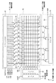
電子機器等が備えるデータを表示する電気光学装置として、液晶表示装置、電気泳動装置、及び有機エレクトロルミネッセンス表示装置等が挙げられる。有機エレクトロルミネッセンス表示装置は、電気光学素子である有機エレクトロルミネッセンス素子を利用して構成されており、図16は、従来の有機エレクトロルミネッセンス表示装置10の構成を示す図である。なお、図16には、有機エレクトロルミネッセンス表示装置10のうち、4本のデータ線X1〜X4及び2本の走査線Y1、Y2に関する部分のみを示している。
【0003】
即ち、この有機エレクトロルミネッセンス表示装置10は、列方向に延びる複数本のデータ線X1〜X4と、行方向に延びる複数本の走査線Y1、Y2と、データ線X1〜X4と平行に延び且つ端部は電源VDDに接続された共通給電線11と、を有しており、データ線X1〜X4と走査線Y1、Y2との各交点に対応して、発色部としての有機エレクトロルミネッセンス素子12、…、12が設けられている。この例では、赤(R)の発色が可能な有機エレクトロルミネッセンス素子12、緑(G)の発色が可能な有機エレクトロルミネッセンス素子12及び青(B)の発色が可能な有機エレクトロルミネッセンス素子12を、最初のデータ線X1にはR、次のデータ線X2にはG、その次のデータ線X3にはB、さらにその次のデータ線X4にはR、という具合に、各データ線X1〜X4に順繰りに対応させており、行方向に並んだ赤の発色が可能な有機エレクトロルミネッセンス素子12、緑の発色が可能な有機エレクトロルミネッセンス素子12及び青の発色が可能な有機エレクトロルミネッセンス素子12の3ドットで一つの画素Pを構成していて、これによって、この有機エレクトロルミネッセンス表示装置10はカラー表示が可能となっている。
【0004】
そして、各有機エレクトロルミネッセンス素子12の陰極側は接地されるとともに、正孔注入側は、Pチャネル型の薄膜MOSトランジスタ(以下、PMOSトランジスタと称す。)13を介して、共通給電線11に接続されている。また、PMOSトランジスタ13のゲートと、対応するデータ線X1〜X4との間が、Nチャネル型の薄膜MOSトランジスタ(以下、NMOSトランジスタと称す。)14を介して接続されるとともに、PMOSトランジスタ13のゲートと、共通給電線11との間に、保持容量15が介在している。さらに、NMOSトランジスタ14のゲートが、対応する走査線Y1、Y2に接続されている。これら有機エレクトロルミネッセンス素子12、PMOSトランジスタ13、NMOSトランジスタ14及び保持容量15によって、いわゆるアクティブマトリックス型の表示画面20が構成されている。
【0005】
走査線Y1、Y2の端部は、走査線駆動回路30に接続されている。走査線駆動回路30は、シフトレジスタ31と、バッファ32とによって構成されていて、シフトレジスタ31の出力がバッファ32を介して各走査線Y1、Y2に供給されるようになっている。よって、シフトレジスタ31のシフト動作に同期して、複数の走査線Y1、Y2が順番に選択されて一つずつ充電及び放電を繰り返すようになっている。
【0006】
これに対し、データ線X1〜X4の端部は、データ線駆動回路40に接続されている。データ線駆動回路40は、シフトレジスタ41と、各データ線X1〜X4に対応した複数のスイッチング素子42、…、42とによって構成されていて、
シフトレジスタ41の出力がスイッチング素子42、…、42に供給されるようになっている。従って、シフトレジスタ41のシフト動作に同期して、スイッチング素子42、…、42が順番に選択されて一つずつオン(導通)及びオフ(遮断)を繰り返すようになっている。
【0007】
各スイッチング素子42、…、42のデータ線X1〜X4の逆側は、ビデオ信号線17R、17G、17Bのいずれかに接続されている。ここで、ビデオ信号線17R〜17Bは、赤(R)、緑(G)、青(B)に対応したアナログのビデオ信号電圧VIDR 、VIDG 、VIDB を供給するための信号線であり、表示画面20に隣接し走査線Y1、Y2と平行に配線されている。よって、各データ線X1〜X4は、自己に接続された有機エレクトロルミネッセンス素子12の発色と同色のビデオ信号電圧VIDR 、VIDG 、VIDB が供給可能となるように、スイッチング素子42を介して、ビデオ信号線17R、17G、17Bのいずれかに接続されている。
【0008】
そして、シフトレジスタ31のシフト動作の周期は、シフトレジスタ41のシフト動作によって全てのデータ線X1、X2、…、Xnの選択が完了したタイミングで、走査線Yiの選択を終え次の走査線Y(i+1)の選択に移行できる周期となっている。
【0009】
以上のような構成であれば、シフトレジスタ31及びシフトレジスタ41のシフト動作によって全ての走査線Y1、Y2、…、Ymが順次選択されるとともに、各走査線Y1〜Ymが選択されている間に全てのデータ線X1、X2、…、Xnが順次選択されるから、表示画面20の全画面を利用して画像を出力することができる。なお、各データ線X1〜Xnにはその選択時に対応するビデオ信号線17R〜17Bからビデオ信号電圧VIDR 、VIDG 、VIDB のいずれかが供給され、そのビデオ信号電圧VIDR 、VIDG 、VIDB が、走査線Yiによって選択されているNMOSトランジスタ14を介して保持容量15に蓄えられ、その保持容量15の充電状態に応じてPMOSトランジスタ13のチャネルが制御され、共通給電線11から各有機エレクトロルミネッセンス素子12に流れる電流値がビデオ信号電圧VIDR 、VIDG 、VIDB に対応した値となるから、各有機エレクトロルミネッセンス素子12を所望の輝度で発光させることができる。
【0010】
【発明が解決しようとする課題】
上記従来の有機エレクトロルミネッセンス表示装置10であっても、表示画面20を利用して画像を出力するという動作に関しては特に問題はなく、むしろ、全画面を利用して画像を出力することに関しては非常に効率的な構成であった。
【0011】
しかしながら、従来の有機エレクトロルミネッセンス表示装置10では、走査線駆動回路30によって走査線Y1、Y2、…、Ymの全てを順次駆動させる一方で、データ線駆動回路40によってデータ線X1、X2、…、Xnの全てを順次駆動させる構成であったため、例えば文字や記号等のキャラクタを表示するような場合でも、全画面に対してデータを書き換えなければならなかった。そして、全画面に対してデータを書き換えるためには、上述したように全データ線X1〜Xn及び全走査線Y1〜Ymを順次駆動させる必要があるが、特にデータ線X1〜Xnは、極短い周期で駆動させなければならないため、データ線X1〜Xnに対しては高速で充電及び放電を繰り返す必要がある。また、走査線Y1〜Ymに関しても、キャラクタを表示しない領域に配線されているものも全て駆動する必要があった。
【0012】
つまり、上記従来の構成では、文字や記号等のキャラクタを表示する際にも、画像を表示する際と同様に消費電力の大きい動作を行わなければならず、また、キャラクタを表示しない領域についても走査線Y1〜Ymを駆動させる構成であったため、無駄な電力を消費してしまう構成となっていた。
【0013】
さらに、表示制御をすることに限らず、断線の検査やプリチャージをする場合にも、無駄な電力を消費してしまう構成となっていた。
【0014】
本発明は、このような従来の技術が有する未解決の課題に着目してなされたものであって、無駄な電力消費を抑えることができる電気光学装置及びその駆動方法、有機エレクトロルミネッセンス表示装置、並びに電子機器を提供することを目的としている。
【0015】
【課題を解決するための手段】
上記目的を達成するために、本発明の第1の電気光学装置は、格子状に配線された複数のデータ線及び走査線と、前記データ線と前記走査線との各交差部に対応して配置された電気光学素子と、を備えた電気光学装置であって、前記データ線を駆動可能なデータ線駆動回路と、前記データ線駆動回路とは別に前記データ線を駆動可能な副データ線駆動回路と、を備えていることを特徴としている。
【0016】
本発明の第2の電気光学装置は、本発明の第1の電気光学装置である電気光学装置において、前記データ線駆動回路には、前記複数のデータ線を接続し、前記副データ線駆動回路には、前記複数のデータ線のうちの一部のみを選択的に接続したことを特徴としている。
【0017】
本発明の第3の電気光学装置は、本発明の第1又は第2の電気光学装置において、前記副データ線駆動回路が、デコーダを備えていることを特徴としている。
【0018】
本発明の第4の電気光学装置は、本発明の第1から第3の電気光学装置において、前記データ線駆動回路及び前記副データ線駆動回路のうち少なくともいずれかが、シフトレジスタを備えていることを特徴としている。
【0019】
本発明の第5の電気光学装置は、本発明の第1から第4の電気光学装置において、前記データ線駆動回路及び前記副データ線駆動回路のうち少なくともいずれかが、ラッチ回路を備えていることを特徴としている。
【0020】
本発明の第6の電気光学装置は、本発明の第1から第5の電気光学装置において、前記データ線駆動回路及び前記副データ線駆動回路のうち少なくともいずれかが、D/Aコンバータ回路を備えていることを特徴としている。
【0021】
本発明の第7の電気光学装置は、本発明の第1から第6の電気光学装置において、前記副データ線駆動回路には、前記複数のデータ線のうち、表示画面の特定領域に配されたデータ線のみを選択的に接続したことを特徴としている。
【0022】
本発明の第8の電気光学装置は、本発明の第1から第7の電気光学装置において、赤の発色が可能な前記電気光学素子、緑の発色が可能な前記電気光学素子及び青の発色が可能な前記電気光学素子の3ドットを1画素とすることによりカラー表示が可能となっており、前記副データ線駆動回路には、前記三色のうちの一部の色に対応したデータ線のみを選択的に接続したことを特徴としている。
【0023】
本発明の第9の電気光学装置は、本発明の第8の電気光学装置において、前記副データ線駆動回路には、前記一部の色に対応したデータ線であって、表示画面の特定領域に配されたデータ線のみを選択的に接続したことを特徴としている。
【0024】
本発明の第10の電気光学装置は、本発明の第1から第9の電気光学装置において、全ドット表示モードとキャラクタ表示モードとの間で切換が可能となっており、前記全ドット表示モードが選択されている場合には、前記データ線駆動回路が有効となり、前記キャラクタ表示モードが選択されている場合には、前記副データ線駆動回路が有効となるようになっていることを特徴としている。
【0025】
本発明の第11の電気光学装置は、本発明の第1から第10の電気光学装置において、前記複数の走査線を駆動可能な走査線駆動回路と、前記走査線駆動回路とは別に前記複数の走査線を駆動可能な副走査線駆動回路とを備え、前記走査線駆動回路には、前記複数の走査線を接続し、前記副走査線駆動回路には、前記複数の走査線のうちの一部のみを選択的に接続したことを特徴としている。
【0026】
本発明の第12の電気光学装置は、本発明の第11の電気光学装置において、前記走査線駆動回路及び前記副走査線駆動回路のうち少なくともいずれかが、デコーダを備えていることを特徴としている。
【0027】
本発明の第13の電気光学装置は、本発明の第11又は第12の電気光学装置において、前記走査線駆動回路及び前記副走査線駆動回路のうち少なくともいずれかが、シフトレジスタを備えていることを特徴としている。
【0028】
本発明の第14の電気光学装置は、本発明の第11から第13の電気光学装置において、前記副走査線駆動回路には、前記複数の走査線のうち、表示画面の特定領域に配された走査線のみを選択的に接続したことを特徴としている。
【0029】
本発明の第15の電気光学装置は、本発明の第11から第14の電気光学装置において、全ドット表示モードとキャラクタ表示モードとの間で切換が可能となっており、前記全ドット表示モードが選択されている場合には、前記データ線駆動回路及び走査線駆動回路が有効となり、前記キャラクタ表示モードが選択されている場合には、前記副データ線駆動回路及び前記副走査線回路が有効となるようになっていることを特徴としている。
【0030】
本発明の第16の電気光学装置は、本発明の第10又は第15の電気光学装置において、前記キャラクタ表示モードが選択されている場合には、前記全ドット表示モードが選択されている場合に比べて、階調数が減じられるようになっていることを特徴としている。
【0031】
本発明の第17の電気光学装置は、本発明の第10、第15及び第16の電気光学装置において、前記キャラクタ表示モードが選択されている場合には、前記全ドット表示モードが選択されている場合に比べて、フレーム周波数が減じられるようになっていることを特徴としている。
【0032】
本発明の第18の電気光学装置は、本発明の第10、第15、第16及び第17の電気光学装置において、前記全ドット表示モードから前記キャラクタ表示モードに移行する際に全画素を一斉にリセットできるようにしたことを特徴としている。
【0033】
本発明の第19の電気光学装置は、本発明の第1から第18の電気光学装置において、一画面分の走査線が駆動される期間内に、前記データ線駆動回路と前記副データ線回路とを切り替えて前記複数のデータ線を駆動することを特徴としている。
【0034】
また、上記目的を達成するために、本発明の第1の電気光学装置の駆動方法は、格子状に配線された複数のデータ線及び複数の走査線と、前記複数のデータ線と前記複数の走査線との各交差部に対応して配置された電気光学素子と、を備えた電気光学装置の駆動方法であって、前記複数のデータ線を駆動可能なデータ線駆動回路と、前記データ線駆動回路とは別に前記複数のデータ線を駆動可能な副データ線駆動回路とを切り替えて前記複数のデータ線を駆動することを特徴としている。
【0035】
本発明の第2の電気光学装置の駆動方法は、本発明の第1の電気光学装置の駆動方法において、前記データ線駆動回路には、前記複数のデータ線を接続し、前記副データ線駆動回路には、前記複数のデータ線のうちの一部のみを選択的に接続したことを特徴としている。
【0036】
本発明の第3の電気光学装置の駆動方法は、本発明の第1又は第2の電気光学装置の駆動方法において、前記副データ線駆動回路が、デコーダを備えていることを特徴としている。
【0037】
本発明の第4の電気光学装置の駆動方法は、本発明の第1から第3の電気光学装置の駆動方法において、前記データ線駆動回路及び前記副データ線駆動回路のうち少なくともいずれかが、シフトレジスタを備えていることを特徴としている。
【0038】
本発明の第5の電気光学装置の駆動方法は、本発明の第1から第4の電気光学装置の駆動方法において、前記データ線駆動回路及び前記副データ線駆動回路のうち少なくともいずれかが、ラッチ回路を備えていることを特徴としている。
【0039】
本発明の第6の電気光学装置の駆動方法は、本発明の第1から第5の電気光学装置の駆動方法において、前記データ線駆動回路及び前記副データ線駆動回路のうち少なくともいずれかが、D/Aコンバータ回路を備えていることを特徴としている。
【0040】
本発明の第7の電気光学装置の駆動方法は、本発明の第1から第6の電気光学装置の駆動方法において、前記副データ線駆動回路には、前記複数のデータ線のうち、表示画面の特定領域に配されたデータ線のみを選択的に接続したことを特徴としている。
【0041】
本発明の第8の電気光学装置の駆動方法は、 本発明の第1から第7の電気光学装置の駆動方法において、赤の発色が可能な前記電気光学素子、緑の発色が可能な前記電気光学素子及び青の発色が可能な前記電気光学素子の3ドットを1画素とすることによりカラー表示が可能となっており、前記副データ線駆動回路には、前記三色のうちの一部の色に対応したデータ線のみを選択的に接続したことを特徴としている。
【0042】
本発明の第9の電気光学装置の駆動方法は、本発明の第8の電気光学装置の駆動方法において、前記副データ線駆動回路には、前記一部の色に対応したデータ線であって、表示画面の特定領域に配されたデータ線のみを選択的に接続したことを特徴としている。
【0043】
本発明の第10の電気光学装置の駆動方法は、本発明の第1から第9の電気光学装置の駆動方法において、全ドット表示モードとキャラクタ表示モードとの間で切換が可能となっており、前記全ドット表示モードが選択されている場合には、前記データ線駆動回路が有効となり、前記キャラクタ表示モードが選択されている場合には、前記副データ線駆動回路が有効となるようになっていることを特徴としている。
【0044】
本発明の第11の電気光学装置の駆動方法は、本発明の第1から第10の電気光学装置の駆動方法において、前記複数の走査線を接続し、当該複数の走査線を駆動可能な走査線駆動回路と、前記複数の走査線のうちの一部のみを選択的に接続し、前記走査線駆動回路とは別に当該一部の走査線を駆動可能な副走査線駆動回路とを切り替えて前記複数の走査線を駆動することを特徴としている。
【0045】
本発明の第12の電気光学装置の駆動方法は、本発明の第11の電気光学装置の駆動方法において、前記走査線駆動回路及び前記副走査線駆動回路のうち少なくともいずれかが、デコーダを備えていることを特徴としている。
【0046】
本発明の第13の電気光学装置の駆動方法は、本発明の第11又は第12の電気光学装置の駆動方法において、前記走査線駆動回路及び前記副走査線駆動回路のうち少なくともいずれかが、シフトレジスタを備えていることを特徴としている。
【0047】
本発明の第14の電気光学装置の駆動方法は、本発明の第11から第13の電気光学装置の駆動方法において、前記副走査線駆動回路には、前記複数の走査線のうち、表示画面の特定領域に配された走査線のみを選択的に接続したことを特徴としている。
【0048】
本発明の第15の電気光学装置の駆動方法は、本発明の第11から第14の電気光学装置の駆動方法において、全ドット表示モードとキャラクタ表示モードとの間で切換が可能となっており、前記全ドット表示モードが選択されている場合には、前記データ線駆動回路及び走査線駆動回路が有効となり、前記キャラクタ表示モードが選択されている場合には、前記副データ線駆動回路及び前記副走査線回路が有効となるようになっていることを特徴としている。
【0049】
本発明の第16の電気光学装置の駆動方法は、本発明の第10又は第15の電気光学装置の駆動方法において、前記キャラクタ表示モードが選択されている場合には、前記全ドット表示モードが選択されている場合に比べて、階調数が減じられるようになっていることを特徴としている。
【0050】
本発明の第17の電気光学装置の駆動方法は、本発明の第10、第15及び第16の電気光学装置の駆動方法において、前記キャラクタ表示モードが選択されている場合には、前記全ドット表示モードが選択されている場合に比べて、フレーム周波数が減じられるようになっていることを特徴としている。
【0051】
本発明の第18の電気光学装置の駆動方法は、本発明の第10、第15、第16及び第17の電気光学装置の駆動方法において、前記全ドット表示モードから前記キャラクタ表示モードに移行する際に全画素を一斉にリセットできるようにしたことを特徴としている。
【0052】
本発明の第19の電気光学装置の駆動方法は、本発明の第1から第18の電気光学装置の駆動方法において、一画面分の走査線が駆動される期間内に、前記データ線駆動回路と前記副データ線回路とを切り替えて前記データ線を駆動することを特徴としている。
【0053】
また、上記目的を達成するために、本発明の第1の有機エレクトロルミネッセンス表示装置は、格子状に配設された複数の行方向配線及び複数のデータ線と、前記複数の行方向配線及び複数のデータ線の各交点に対応して設けられた有機エレクトロルミネッセンス素子と、前記複数のデータ線を駆動可能なデータ線駆動回路と、前記複数の行方向配線を駆動可能な行駆動回路と、を備えた有機エレクトロルミネッセンス表示装置において、
前記データ線駆動回路とは別に、デコーダを含んで構成されたデータ線駆動用の副データ線駆動回路を設け、前記データ線駆動回路には、前記複数のデータ線を接続し、前記副データ線駆動回路には、前記複数のデータ線のうちの一部のみを選択的に接続したことを特徴としている。
【0054】
本発明の第2の有機エレクトロルミネッセンス表示装置は、格子状に配設された複数の行方向配線及び複数のデータ線と、前記複数の行方向配線及び複数のデータ線の各交点に対応して設けられた有機エレクトロルミネッセンス素子と、前記複数のデータ線を駆動可能なデータ線駆動回路と、前記行方向配線を駆動可能な行駆動回路と、を備えた有機エレクトロルミネッセンス表示装置において、前記データ線駆動回路とは別に、シフトレジスタを含んで構成されたデータ線駆動用の副データ線駆動回路を設け、前記データ線駆動回路には、前記複数のデータ線を接続し、前記副データ線駆動回路には、前記複数のデータ線のうちの一部のみを選択的に接続したことを特徴としている。
【0055】
本発明の第3の有機エレクトロルミネッセンス表示装置は、本発明の第1又は第2の有機エレクトロルミネッセンス表示装置において、前記データ線駆動回路を、シフトレジスタを含んで構成したことを特徴としている。
【0056】
本発明の第4の有機エレクトロルミネッセンス表示装置は、本発明の第1から第3の有機エレクトロルミネッセンス表示装置において、前記行駆動回路を、デコーダを含んで構成したことを特徴としている。
【0057】
本発明の第5の有機エレクトロルミネッセンス表示装置は、本発明の第1から第4の有機エレクトロルミネッセンス表示装置において、前記副データ線駆動回路には、前記複数のデータ線のうち、表示画面の特定領域に配されたデータ線のみを選択的に接続したことを特徴としている。
【0058】
本発明の第6の有機エレクトロルミネッセンス表示装置は、本発明の第1から第5の有機エレクトロルミネッセンス表示装置において、赤の発色が可能な前記有機エレクトロルミネッセンス素子、緑の発色が可能な前記有機エレクトロルミネッセンス素子及び青の発色が可能な前記有機エレクトロルミネッセンス素子の3ドットを1画素とすることによりカラー表示が可能となっており、前記副データ線駆動回路には、前記三色のうちの一部の色に対応したデータ線のみを選択的に接続したことを特徴としている。
【0059】
本発明の第7の有機エレクトロルミネッセンス表示装置は、本発明の第6の有機エレクトロルミネッセンス表示装置において、前記一部の色は緑であることを特徴としている。
【0060】
本発明の第8の有機エレクトロルミネッセンス表示装置は、本発明の第6又は第7の有機エレクトロルミネッセンス表示装置において、前記副データ線駆動回路には、前記一部の色に対応したデータ線であって、表示画面の特定領域に配されたデータ線のみを選択的に接続したことを特徴としている。
【0061】
本発明の第9の有機エレクトロルミネッセンス表示装置は、本発明の第1から第8の有機エレクトロルミネッセンス表示装置において、全ドット表示モードとキャラクタ表示モードとの間で切換が可能となっており、前記全ドット表示モードが選択されている場合には、前記データ線駆動回路が有効となり、前記キャラクタ表示モードが選択されている場合には、前記副データ線駆動回路が有効となるようになっていることを特徴としている。
【0062】
本発明の第10の有機エレクトロルミネッセンス表示装置は、本発明の第1から第8の有機エレクトロルミネッセンス表示装置において、前記行駆動回路とは別に、デコーダを含んで構成された行方向配線駆動用の副行駆動回路を設け、前記行駆動回路には、前記複数の行方向配線を接続し、前記副行駆動回路には、前記複数の行方向配線のうちの一部のみを選択的に接続したことを特徴としている。
【0063】
本発明の第11の有機エレクトロルミネッセンス表示装置は、本発明の第1から第8の有機エレクトロルミネッセンス表示装置において、前記行駆動回路とは別に、シフトレジスタを含んで構成された行方向配線駆動用の副行駆動回路を設け、前記行駆動回路には、前記複数の行方向配線を接続し、前記副行駆動回路には、前記複数の行方向配線のうちの一部のみを選択的に接続したことを特徴としている。
【0064】
本発明の第12の有機エレクトロルミネッセンス表示装置は、本発明の第10又は第11の有機エレクトロルミネッセンス表示装置において、前記副行駆動回路には、前記複数の行方向配線のうち、表示画面の特定領域に配された行方向配線のみを選択的に接続したことを特徴としている。
【0065】
本発明の第13の有機エレクトロルミネッセンス表示装置は、本発明の第11から第12の有機エレクトロルミネッセンス表示装置において、全ドット表示モードとキャラクタ表示モードとの間で切換が可能となっており、前記全ドット表示モードが選択されている場合には、前記データ線駆動回路及び行駆動回路が有効となり、前記キャラクタ表示モードが選択されている場合には、前記副データ線駆動回路及び前記副行駆動回路が有効となるようになっていることを特徴としている。
【0066】
本発明の第14の有機エレクトロルミネッセンス表示装置は、本発明の第9又は第13の有機エレクトロルミネッセンス表示装置において、前記キャラクタ表示モードが選択されている場合には、前記全ドット表示モードが選択されている場合に比べて、階調数が減じられるようになっていることを特徴としている。
【0067】
本発明の第15の有機エレクトロルミネッセンス表示装置は、本発明の第9、第13及、第14の有機エレクトロルミネッセンス表示装置において前記キャラクタ表示モードが選択されている場合には、前記全ドット表示モードが選択されている場合に比べて、フレーム周波数が減じられるようになっていることを特徴としている。
【0068】
本発明の第16の有機エレクトロルミネッセンス表示装置は、本発明の第9、第13、第14及び第15の有機エレクトロルミネッセンス表示装置において、前記全ドット表示モードから前記キャラクタ表示モードに移行する際に全画素を一斉にリセットできるようにしたことを特徴としている。
【0069】
また、上記目的を達成するために、本発明の電子機器は、データを表示する表示装置を備えている電子機器であって、前記表示装置は、本発明の第1から第19の電気光学装置又は本発明の第1から第16の有機エレクトロルミネッセンス表示装置を使用した電気光学表示装置からなるようにしたことを特徴としている。
【0070】
ここで、本発明の第1の電気光学装置及び電気光学装置の駆動方法にあっては、本来のデータ線駆動回路の他に、副データ線駆動回路を備えることで、データ線駆動回路と副データ線駆動回路とをデータ線の表示形態等に応じて選択的に利用する、という使用態様が可能となる。すなわち、本来の目的として駆動されるデータ線駆動回路の他に、他の用途、例えば回路等の検査回路やプリチャージ回路としても使用できる副データ線駆動回路を備えて、この副データ線駆動回路が選択的に利用可能になっている。
【0071】
また、本発明の第2の電気光学装置及び電気光学装置の駆動方法にあっては、副データ線駆動回路には、データ線の一部のみを選択的に接続しているから、全データ線によって表示を行う場合にはデータ線駆動回路を利用し、一部のデータ線によって表示を行う場合には副データ線駆動回路を利用する、という使用態様が可能となる。
【0072】
また、本発明の第3の電気光学装置及び電気光学装置の駆動方法にあっては、副データ線駆動回路が、デコーダを含んで構成されているから、それに接続されたデータ線のうちの任意のデータ線を選択的に駆駆動させることもできる。
【0073】
また、本発明の第4の電気光学装置及び電気光学装置の駆動方法にあっては、データ線駆動回路及び副データ線駆動回路のうち少なくともいずれかが、シフトレジスタを含んで構成されているから、シフトレジスタを含んで構成されたデータ線駆動回路又は副データ線駆動回路を動作させるために配線を多く設けなくても済む。
【0074】
また、本発明の第5の電気光学装置及び電気光学装置の駆動方法にあっては、データ線駆動回路及び副データ線駆動回路のうち少なくともいずれかが、ラッチ回路を含んで構成されているから、例えば、アドレス線を設けることなく、所望のデータ線又は走査線を駆動させることができる。
【0075】
また、本発明の第6の電気光学装置及び電気光学装置の駆動方法にあっては、データ線駆動回路及び副データ線駆動回路のうち少なくともいずれかが、D/Aコンバータ回路を含んで構成されていることから、例えば、電気光学装置自体にD/Aコンバータ回路を備えなくて済む。
【0076】
また、本発明の第7の電気光学装置及び電気光学装置の駆動方法にあっては、副データ線駆動回路に接続されているデータ線は、画面の特定領域(データ線が画面縦方向に延びているものとすると、例えば、画面の左側、中央、右側といった領域)に配されたデータ線であるから、その副データ線駆動回路を利用してデータ線を駆動させる状況では、画面の特定領域に限って表示を行うことができる。
【0077】
一方、本発明の第8の電気光学装置及び電気光学装置の駆動方法にあっては、副データ線駆動回路を利用してデータ線を駆動させる状況では、一部の色のみを利用して表示を行うことができる。
【0078】
そして、本発明の第9の電気光学装置及び電気光学装置の駆動方法にあっては、副データ線駆動回路を利用してデータ線を駆動させる状況では、画面の特定領域に、一部の色のみを利用して表示を行うことができる。
【0079】
本発明の第10の電気光学装置及び電気光学装置の駆動方法にあっては、画面を構成する全ドットを利用して画像を出力する全ドット表示モードと、文字や記号等の比較的簡易な図形であるキャラクタを表示するキャラクタ表示モードとの二つの表示モードが選択可能であり、本発明の第8の電気光学装置及び電気光学装置の駆動方法に係る発明の構成を備えている場合には、前者はカラー表示モード、後者は一部色(単色)表示モード、と表現することもできる。
【0080】
そして、本発明の第10の電気光学装置及び電気光学装置の駆動方法では、全ドット表示モードを、本来のデータ線駆動回路に対応させ、キャラクタ表示モードを、副データ線駆動回路に対応させている。このため、全ドット表示モードが選択されている状況では、全てのデータ線を利用して表示が行われ、キャラクタ表示モードが選択されている状況では、一部のデータ線を利用して表示が行われることになるから、各表示モードの表示レベルと、利用されるデータ線の本数との整合がとれる。
【0081】
さらに、本発明の第11の電気光学装置及び電気光学装置の駆動方法にあっては、本来の行駆動回路の他に、副行駆動回路を有し、その副行駆動回路には、行方向配線の一部のみを選択的に接続しているから、全ての行方向配線によって表示を行う場合には行駆動回路を利用し、一部の行方向配線によって表示を行う場合には副行駆動回路を利用する、という使用態様が可能となる。
【0082】
さらにまた、本発明の第12の電気光学装置及び電気光学装置の駆動方法にあっては、走査線駆動回路及び副走査線駆動回路のうち少なくともいずれかが、デコーダを含んで構成されているから、それに接続された走査線のうちの任意の走査線を選択的に駆動させることもできる。
【0083】
そして、本発明の第13の電気光学装置及び電気光学装置の駆動方法にあっては、走査線駆動回路及び副走査線駆動回路のうち少なくともいずれかが、シフトレジスタを含んで構成されているから、シフトレジスタを含んで構成された走査線駆動回路及び副走査線駆動回路を動作させるために配線を多く設けなくても済む。
【0084】
そしてまた、本発明の第14の電気光学装置及び電気光学装置の駆動方法にあっては、副走査線駆動回路に接続されている走査線は、画面の特定領域(走査線が画面横方向に延びているものとすると、例えば、画面の上段、中段、下段といった領域)に配された走査線であるから、その副走査線駆動回路を利用して走査線を駆動させる状況では、画面の特定領域に限って表示を行うことができる。従って、この本発明の第14の電気光学装置及び電気光学装置の駆動方法が、上記本発明の第7の電気光学装置及び電気光学装置の駆動方法の構成を備えていれば、画面の左上段、中央上段、右下段、というようなさらに細かい領域を特定領域とすることができる。
【0085】
本発明の第15の電気光学装置及び電気光学装置の駆動方法にあっては、全ドット表示モードを、本来の走査線駆動回路に対応させ、キャラクタ表示モードを、副走査線駆動回路に対応させているから、全ドット表示モードが選択されている状況では、全ての走査線を利用して表示が行われ、キャラクタ表示モードが選択されている状況では、一部の走査線を利用して表示が行われることになり、各表示モードの表示レベルと、利用される走査線の本数との整合がとれる。
【0086】
そして、本発明の第16の電気光学装置及び電気光学装置の駆動方法にあっては、例えば、キャラクタ表示モードが選択されている場合には、階調数を最低の2(つまり、各電気光学素子は、発色しているか、発色していないかの二状態しかない。)とし、全ドット表示モードが選択されている場合には、階調数を3以上とする、という使用態様も採用できる。
【0087】
また、本発明の第17の電気光学装置及び電気光学装置の駆動方法にあっては、キャラクタ表示モードが選択されている場合には、フレーム周波数を減らし、その分、走査線やデータ線の選択期間(駆動させている期間)を長くすることができる。
【0088】
さらに、本発明の第18の電気光学装置及び電気光学装置の駆動方法にあっては、一斉にリセットできるようにしたため、画像を消去するために全画面を走査する動作が不要となり、かかる全画面を操作する際に消費される余分な消費電力を抑えることができる。また、キャラクタ表示モードに移行し文字や記号等が表示されたときに、それら文字や記号等の判別を困難にするノイズが画面に残るようなことが防止される。
【0089】
また、本発明の第19の電気光学装置及び電気光学装置の駆動方法にあっては、一画面分の走査線が駆動される期間内に、データ線駆動回路と副データ線回路とを切り替えてデータ線を駆動することで、一画面内の表示期間内にデータ線駆動回路による画像と副データ線駆動回路による画像とを表示することができる。例えば、ここで、データ線駆動回路と副データ線駆動回路との駆動時期については、走査線駆動期間の前半にデータ線駆動回路によりデータ線を駆動し、後半に副データ線駆動回路によりデータ線を駆動したり、その逆に、前半に副データ線駆動回路によりデータ線を駆動し、後半にデータ線駆動回路によりデータ線を駆動したりする。
【0090】
また、本発明の第1の有機エレクトロルミネッセンス表示装置にあっては、本来のデータ線駆動回路の他に、副データ線駆動回路を有し、その副データ線駆動回路には、データ線の一部のみを選択的に接続しているから、全データ線によって表示を行う場合にはデータ線駆動回路を利用し、一部のデータ線によって表示を行う場合には副データ線駆動回路を利用する、という使用態様が可能となる。しかも、副データ線駆動回路は、デコーダを含んで構成されているから、それに接続されたデータ線のうちの任意のデータ線を選択的に駆動させることもできる。
【0091】
また、本発明の第2の有機エレクトロルミネッセンス表示装置にあっても、副データ線駆動回路を有し、その副データ線駆動回路にデータ線の一部のみを選択的に接続しているから、全データ線によって表示を行う場合にはデータ線駆動回路を利用し、一部のデータ線によって表示を行う場合には副データ線駆動回路を利用する、という使用態様が可能となる。また、この本発明の第2有機エレクトロルミネッセンス表示装置では、副データ線駆動回路は、シフトレジスタを含んで構成されているから、その副データ線駆動回路を動作させるために多くの配線を設けなくても済む。
【0092】
本発明の第3の有機エレクトロルミネッセンス表示装置にあっては、データ線駆動回路をシフトレジスタを含んで構成しているから、それによって駆動されるデータ線の本数が多数であっても、データ線駆動回路を動作させるための配線数を極端に多くしないで済む。
【0093】
また、本発明の第4の有機エレクトロルミネッセンス表示装置にあっては、行駆動回路をデコーダによって構成しているため、副データ線駆動回路を利用する場合に、必要な行方向配線だけを駆動させるという使用態様も可能となる。
【0094】
なお、この本発明の第4の有機エレクトロルミネッセンス表示装置では、本来のデータ線駆動回路を利用して画面全体に画像を出力する場合にも、デコーダによって行方向配線を順に選択し駆動させる必要がある。しかし、行方向配線の駆動周期は、データ線の駆動周期に比べて大幅に長いため、デコーダに接続されるアドレス選択用の配線が多数であっても、それらアドレス選択用の配線の充電及び放電の周期が極端に短くなる訳ではないから、アドレス選択用の配線の駆動に伴って消費電力が極端に大きくなるようなことはない。
【0095】
そして、本発明の第5の有機エレクトロルミネッセンス表示装置にあっては、副データ線駆動回路に接続されているデータ線は、画面の特定領域(データ線が画面縦方向に延びているものとすると、例えば、画面の左側、中央、右側といった領域)に配されたデータ線であるから、その副データ線駆動回路を利用してデータ線を駆動させる状況では、画面の特定領域に限って表示を行うことができる。
【0096】
一方、本発明の第6の有機エレクトロルミネッセンス表示装置にあっては、副データ線駆動回路を利用してデータ線を駆動させる状況では、一部の色のみを利用して表示を行うことができる。特に、本発明の第7の有機エレクトロルミネッセンス表示装置では、副データ線駆動回路を利用してデータ線を駆動させる状況では、現在報告されている有機EL材料の中で最も発光輝度及び発光効率の良い緑(G)によって表示が行われる。
【0097】
そして、本発明の第8の有機エレクトロルミネッセンス表示装置にあっては、副データ線駆動回路を利用してデータ線を駆動させる状況では、画面の特定領域に、一部の色のみを利用して表示を行うことができる。
【0098】
本発明の第9の有機エレクトロルミネッセンス表示装置にあっては、画面を構成する全ドットを利用して画像を出力する全ドット表示モードと、文字や記号等の比較的簡易な図形であるキャラクタを表示するキャラクタ表示モードとの二つの表示モードが選択可能であり、本発明の第6又は第7の有機エレクトロルミネッセンス表示装置の構成を備えている場合には、前者はカラー表示モード、後者は一部色(単色)表示モード、と表現することもできる。
【0099】
そして、本発明の第9の有機エレクトロルミネッセンス表示装置では、全ドット表示モードを、本来のデータ線駆動回路に対応させ、キャラクタ表示モードを、副データ線駆動回路に対応させている。このため、全ドット表示モードが選択されている状況では、全てのデータ線を利用して表示が行われ、キャラクタ表示モードが選択されている状況では、一部のデータ線を利用して表示が行われることになるから、各表示モードの表示レベルと、利用されるデータ線の本数との整合がとれる。
【0100】
さらに、本発明の第10の有機エレクトロルミネッセンス表示装置にあっては、本来の行駆動回路の他に、副行駆動回路を有し、その副行駆動回路には、行方向配線の一部のみを選択的に接続しているから、全ての行方向配線によって表示を行う場合には行駆動回路を利用し、一部の行方向配線によって表示を行う場合には副行駆動回路を利用する、という使用態様が可能となる。しかも、副行駆動回路は、デコーダを含んで構成されているから、それに接続された行方向配線のうちの任意の行方向配線を選択的に駆動させることもできる。
【0101】
また、本発明の第11の有機エレクトロルミネッセンス表示装置にあっても、副行駆動回路を有し、その副行駆動回路に行方向配線の一部のみを選択的に接続しているから、全ての行方向配線によって表示を行う場合には行駆動回路を利用し、一部の行方向配線によって表示を行う場合には副行駆動回路を利用する、という使用態様が可能となる。また、この本発明の第11の有機エレクトロルミネッセンス表示装置では、副行駆動回路は、シフトレジスタを含んで構成されているから、その副行駆動回路を動作させるために多くの配線を設けなくても済む。
【0102】
そして、本発明の第12の有機エレクトロルミネッセンス表示装置にあっては、副行駆動回路に接続されている行方向配線は、画面の特定領域(行方向配線が画面横方向に延びているものとすると、例えば、画面の上段、中段、下段といった領域)に配された行方向配線であるから、その副行駆動回路を利用して行方向配線を駆動させる状況では、画面の特定領域に限って表示を行うことができる。従って、この本発明の第12の有機エレクトロルミネッセンス表示装置が、上記本発明の第5の有機エレクトロルミネッセンス表示装置の構成を備えていれば、画面の左上段、中央上段、右下段、というようなさらに細かい領域を特定領域とすることができる。
【0103】
本発明の第13の有機エレクトロルミネッセンス表示装置にあっては、全ドット表示モードを、本来の行駆動回路に対応させ、キャラクタ表示モードを、副行駆動回路に対応させているから、全ドット表示モードが選択されている状況では、全ての行方向配線を利用して表示が行われ、キャラクタ表示モードが選択されている状況では、一部の行方向配線を利用して表示が行われることになり、各表示モードの表示レベルと、利用される行方向配線の本数との整合がとれる。
【0104】
そして、本発明の第14の有機エレクトロルミネッセンス表示装置にあっては、例えば、キャラクタ表示モードが選択されている場合には、階調数を最低の2(つまり、各有機EL素子は、発色しているか、発色していないかの二状態しかない。)とし、全ドット表示モードが選択されている場合には、階調数を3以上とする、という使用態様も採用できる。
【0105】
また、本発明の第15の有機エレクトロルミネッセンス表示装置にあっては、キャラクタ表示モードが選択されている場合には、フレーム周波数を減らし、その分、行方向配線やデータ線の選択期間(駆動させている期間)を長くすることができる。
【0106】
さらに、本発明の第16の有機エレクトロルミネッセンス表示装置にあっては、一斉にリセットできるようにしたため、画像を消去するために全画面を走査する動作が不要となり、かかる全画面を操作する際に消費される余分な消費電力を抑えることができる。また、キャラクタ表示モードに移行し文字や記号等が表示されたときに、それら文字や記号等の判別を困難にするノイズが画面に残るようなことが防止される。
【0107】
本発明の第20の電気光学装置の駆動方法は、1水平走査期間内に前記データ線駆動回路と前記副データ線駆動回路とを切り替えて前記データ線を駆動することを特徴とする。例えば、1水平走査期間内に画像信号などのデータ数の多い情報を前記データ線駆動回路を介して供給する期間と、文字情報を前記副データ線駆動回路を介して供給する期間と、を設けることができる。この場合、画像信号などデータ数の多い情報を供給する期間を、文字情報を供給する期間に比べて長めに設定することが好ましい。
【0108】
また、本発明の電子機器は、データを表示する表示装置を備えている電子機器であり、表示装置として、上記本発明の第1から第19の電気光学装置又は上記本発明の第1から第16の有機エレクトロルミネッセンス表示装置を使用したことで、本発明が適用されたことによる電気光学装置又は有機エレクトロルミネッセンス表示装置における上記効果をもつことができる。
【0109】
【発明の実施の形態】
以下、本発明の実施の形態を図面に基づいて説明する。
【0110】
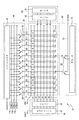
図1は本発明の第1の実施の形態の構成を示す図であって、有機エレクトロルミネッセンス表示装置10の構成を示す回路図である。なお、図16に示した従来の有機エレクトロルミネッセンス表示装置と同じ構成には同じ符号を付し、その同じ構成に関する詳細な説明は省略する。
【0111】
即ち、本実施の形態の有機エレクトロルミネッセンス表示装置10であっても、複数のデータ線X1、X2、…、Xnと、行方向配線としての複数の走査線Y1、Y2、…、Ymとが格子状に配設され、それらデータ線X1〜Xnと走査線Y1〜Ymとの各交点に、図16の場合と同様にR、G、Bの各色に対応した有機エレクトロルミネッセンス素子や保持容量等が配されており、そして、データ線X1〜Xn用のデータ線駆動回路40と、走査線Y1〜Ym駆動用の、行駆動回路としての走査線駆動回路30とを備えている。
【0112】
但し、本実施の形態では、走査線駆動回路30は、シフトレジスタではなく、デコーダ33を含んで構成されている。従って、デコーダ33の動作を適宜制御することにより、走査線Y1〜Ymをシフトレジスタを用いた場合と同様に順番に駆動させることも可能であるし、任意の走査線Y1〜Ymを任意のタイミングで駆動させることも可能である。
【0113】
また、データ線駆動回路40のシフトレジスタ41にはイネーブル信号EnblXが供給され、走査線駆動回路30のデコーダ33にはイネーブル信号EnblYが供給されるようになっている。ここで、データ線駆動回路40は、例えば、画素部とされる表示画面20と同一基板上に一体とされて配置されている。
【0114】
イネーブル信号EnblX及びEnblYは、通常はローレベル(論理値“0”)の信号であって、ローレベルのイネーブル信号EnblX及びEnblYが供給されている間は、シフトレジスタ41及びデコーダ33は、通常の動作を行うようになっている。これに対し、ハイレベル(論理値“1”)のイネーブル信号EnblXが供給されているシフトレジスタ41は、スイッチング素子42の全てを同時にオン状態とするようになっており、ハイレベルのイネーブル信号EnblYが供給されているデコーダ33は、全ての走査線Y1〜Ymを同時に駆動させるようになっている。
【0115】
なお、ハイレベルのイネーブル信号EnblXが生成されている間は、ビデオ信号線17R〜17B上のビデオ信号電圧VIDR 、VIDG 、VIDB は、全てハイレベル(アナログ電圧信号であるため、正確には、取り得る範囲の最高電位)に固定されるようになっている。
【0116】
また、この有機エレクトロルミネッセンス表示装置10は、ビデオ信号線17R〜17B上のビデオ信号電圧VIDR 、VIDG 、VIDBをアナログ信号としてデータ線X1〜Xn用に出力するいわゆるアナログ階調方式を採用しており、この場合、D/Aコンバータ回路を備えることになるが、D/Aコンバータ回路は、例えば、データ線駆動回路40が備えてもよく、或いは、シフトレジスタ41とスイッチング素子42、…、42が表示画面20に一体とされた一体とされたデータ線駆動回路40とは別に配置されて、外付けのICドライバの一部としてされているような構成でもよい。
【0117】
そして、有機エレクトロルミネッセンス表示装置10は、データ線駆動回路40とは別に、副データ線駆動回路50を備えている。この副データ線駆動回路50は、例えば、表示画面20と同一基板上に一体とされて配置されている。
【0118】
副データ線駆動回路50は、デコーダ51と、複数のスイッチング素子52、…、52とを含んで構成されていて、デコーダ51の出力がスイッチング素子52、…、52に供給されるようになっている。従って、デコーダ51の出力に応じて、任意のスイッチング素子52、…、52が任意のタイミングでオン・オフするようになっている。
【0119】
スイッチング素子52、…、52の一端側は、データ線X1〜Xnのうち、緑(G)の発色が可能な有機エレクトロルミネッセンス素子に対応したデータ線X2、X5、X8、…、X(n−1)に接続されている。つまり、データ線駆動回路40には、データ線X1〜Xnの全てが接続されているが、副データ線駆動回路50には、データ線X1〜Xnの一部であるGの発色が可能な有機エレクトロルミネッセンス素子に対応したデータ線X2、X5、X8、…、X(n−1)のみが選択的に接続されている。
【0120】
また、スイッチング素子52、…、52の他端側は、有機エレクトロルミネッセンス素子を発色させるためのキャラクタ表示用電圧VCHR が供給される電源配線53に接続されている。なお、本実施の形態では、従来(図16参照)と同様に、有機エレクトロルミネッセンス素子12と共通給電線11との間にPMOSトランジスタ13を設けた構成であるから、キャラクタ表示用電圧VCHR は、有機エレクトロルミネッセンス素子を発光させる際にはローレベルの電圧(例えば、接地電圧)となり、有機エレクトロルミネッセンス素子を消灯させる際にはハイレベルの電圧となる。
【0121】
本実施の形態の有機エレクトロルミネッセンス表示装置10の基本構成は上記の通りであるが、その使用態様としては、表示画面20の全ドットを使用して画像を表示するモード(全ドット表示モード、若しくはカラー表示モード)と、表示画面20のうち緑(G)のみを発光させて文字や記号等を表示するモード(キャラクタ表示モード、若しくは単色表示モード)との、二つのモードを設定し使い分ける態様が考えられる。
【0122】
そして、前者のカラー表示モードは、走査線駆動回路30とデータ線駆動回路40とが有効となって表示画面20の表示制御が行われ、後者の単色表示モードでは、走査線駆動回路30と副データ線駆動回路50とが有効となって表示画面20の表示制御が行われるようにする。
【0123】
この場合、カラー表示モードでは、アナログ電圧であるビデオ信号電圧VIDR 、VIDG 、VIDB によって発光が制御されることになるから、各色毎に例えば8段階の階調が与えられる。これに対し、単色モードでは、ローレベル及びハイレベルの二段階に変化するキャラクタ表示用電圧VCHR によって発光が制御されることになるから、有機エレクトロルミネッセンス素子には、発色しているか、発色していないかの二状態しかない、つまり階調数は2となっている。このように、単色表示モードが選択されている場合には、カラー表示モードが選択されている場合に比べて、階調数が減じられることになる。
【0124】
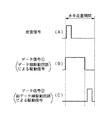
図2は、本実施の形態における有機エレクトロルミネッセンス表示装置10の各信号の状態を示す波形図であって、カラー表示モード選択期間T1から単色表示モード選択期間T2に移行する際を示している。
【0125】
カラー表示モード選択期間T1では、走査線駆動回路30及びデータ線駆動回路40が有効となっていて、走査線駆動回路30のデコーダ33が各走査線Y1〜Ymを順番に駆動するとともに、走査線Y1〜Ymの一つが駆動されている間に、データ線駆動回路40のシフトレジスタ41が、スイッチング素子42、…、42を順番に一つずつオンとする動作を全てのスイッチング素子42、…、42に対して行う。図2のカラー表示モード選択期間T1では、走査線Y1〜Y6が順番に駆動されている様子が示されており、実際には、全ての走査線Y1〜Ymが同様に駆動され、一つの走査線Yiが駆動されている間に、全てのデータ線X1〜Xnが一つずつ順番に高速で駆動される。
【0126】
また、カラー表示モード選択期間T1では、走査線Y1〜Ym及びデータ線X1〜Xnの駆動タイミングに同期し、表示したい画像データを各画素毎及び原色毎にアナログ電圧で表現したビデオ信号電圧VIDR 、VIDG 、VIDB が、高速で切り換えられる。
【0127】
このため、データ線駆動回路40によるデータ線X1〜Xnの駆動が一巡する毎に、一つの走査線Yi分の画像データが表示画面20に出力され、走査線駆動回路30による走査線Y1〜Ymの駆動が一巡する毎に、全画面分の画像データが表示画面20に出力される。
【0128】
カラー表示モード選択期間T1から単色表示モード期間T2に移行するときには、先ず、それまでローレベルであったイネーブル信号EnblX及びEnblYが、ハイレベルとなる。すると、デコーダ回路33は全ての走査線Y1〜Ymを同時に駆動させ、シフトレジスタ41は全てのスイッチング素子42、…、42をオン状態とする。このとき、ビデオ信号電圧VIDR 、VIDG 、VIDB もハイレベルに固定される。よって、表示画面20内の全ての保持容量にハイレベルの電圧が充電されて、有機エレクトロルミネッセンス素子と共通給電線との間が遮断されるから、全ての有機エレクトロルミネッセンス素子は非発光状態となる。つまり、表示画面20内の全ての画素が一斉にリセットされることになる。
【0129】
かかるリセット動作が保証される時間が経過した後に、ハイレベルであったイネーブル信号EnblX及びEnblYは再びローレベルに戻り、それ以降はローレベルに固定される。イネーブル信号EnblX及びEnblYがローレベルに戻ると、デコーダ回路31は全ての走査線Y1〜Ymを同時にローレベルに戻し、シフトレジスタ41は全てのスイッチング素子42、…、42を同時にオフ状態に戻す。このとき、ビデオ信号電圧VIDR 、VIDG 、VIDB もローレベルに戻され、それ以降はローレベルに固定される。
【0130】
次に、データ線駆動回路40の代わりに、副データ線駆動回路50が有効となり、単色表示モード期間T2における表示制御が開始される。
【0131】
そして、単色表示モード期間T2では、デコーダ33により任意の走査線Y1〜Ymが任意のタイミングで駆動され、デコーダ51によりGに対応した任意のデータ線X2、X5、X8、…、X(n−1)と電源配線53との間が任意のタイミングで接続されることになるから、任意の保持容量に任意のタイミングで充電を行うことができる。このとき、電源配線53にはローレベルのキャラクタ表示用電圧VCHR が供給されているから、デコーダ33及び51によって選択された保持容量には、ローレベルの電圧が保持され、有機エレクトロルミネッセンス素子と共通給電線との間が導通して、その有機エレクトロルミネッセンス素子は発光状態となる。
【0132】
つまり、単色表示モード期間T2では、任意のドット(但し、Gのみ)だけを点灯することができるから、表示したい文字や記号等のキャラクタの形状に合わせて任意のドットを点灯させることにより、表示画面20にキャラクタが出力される。
【0133】
このように、電源配線53にローレベルのキャラクタ表示用電圧VCHR を供給した状態で、ランダムアクセスが可能なデコーダ33及び51によって消灯している任意のドットを選択すると、そのドットは消灯状態から点灯状態に移行するし、また、電源配線53にハイレベルのキャラクタ表示用電圧VCHR を供給した状態でデコーダ33及び51によって点灯している任意のドットを選択すると、そのドットは点灯状態から消灯状態に移行するから、キャラクタを新たに表示した部分や書き換えたい部分だけを順次選択しながらキャラクタ表示を行うことができる。
【0134】
従って、本実施の形態の構成であれば、単色表示モード期間T2でキャラクタ表示を行う際には、必要な走査線Y1〜Ym及びデータ線X2、X5、…、Xnだけを駆動させれば済むため、表示に関係しない領域に配線された走査線やデータ線を無駄に駆動させる必要がなく、その分、消費電力の低減が図られる。
【0135】
また、駆動させる必要のある走査線及びデータ線の本数が少なくなれば、フレーム周波数を減らすことも可能であり、フレーム周波数が減った分、走査線Y1〜Ymやデータ線X2、X5、…、Xnの選択期間を長くできる(図2には、カラー表示モード期間T1に比べて単色表示モード期間T2の方が、走査線の選択期間が長くなっている様子が示されている。)から、充電や放電に要する時間を長く設定でき、高速で駆動させる場合に比べて消費電力を低減することができる。
【0136】
さらに、本実施の形態では、単色表示モード期間T2では、単色(Gのみ)でキャラクタを表示するようになっており、しかも階調数を2として中間調を使用しないようになっているから、フルカラーでキャラクタを表示していた従来の有機エレクトロルミネッセンス表示装置に比べて、消費電力を大幅に低減することができる。
【0137】
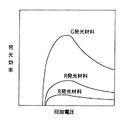
また、単色表示モードでは緑(G)を利用する構成であり、現在実用に供されているGの発光材料は、Rの発光材料やBの発光材料に比べて、図3に示すように発光輝度に優れるとともに、図4に示すように発光効率にも優れている。このため、キャラクタを表示する際に同程度の輝度や発光量を得るためには、本実施の形態のようにGの発光材料を利用することが、他の材料を利用することに比べて最も消費電力を小さくできるのである。
【0138】
以上のように、本実施の形態の構成であれば、種々の点で消費電力の低減が図られているから、全体として、従来の有機エレクトロルミネッセンス表示装置に比べて、格別の低消費電力化を図ることができ、その結果、携帯情報端末(携帯電話)のように少しでも消費電力の低減が必要な電子機器用の表示装置として特に好適である。
【0139】
図5は、本発明の第2の実施の形態を示す図であって、有機エレクトロルミネッセンス表示装置10の構成を示す回路図である。なお、上記第1の実施の形態と同じ構成には、同じ符号を付し、その重複する説明は省略する。
【0140】
先ず、本実施の形態の有機エレクトロルミネッセンス表示装置10の基本的な構成は、上記第1の実施の形態と同様であり、異なるのは、走査線駆動回路30を、シフトレジスタ31を含んで構成した点と、副データ線駆動回路50に、Gの発色が可能な有機エレクトロルミネッセンス素子に対応したデータ線X2、X5、X8、…、X(n−1)のうちの一部のみを選択的に接続した点と、走査線駆動回路30とは別に、副行駆動回路としての副走査線駆動回路60を設けた点と、の三つである。
【0141】
即ち、走査線駆動回路30は、図16に示した従来の有機エレクトロルミネッセンス表示装置10の場合と同様に、シフトレジスタ31及びバッファ32によって構成されている。但し、シフトレジスタ31には、上記第1の実施の形態と同様のイネーブル信号EnblYが入力されるようになっており、ハイレベルのイネーブル信号EnblYが入力されると、シフトレジスタ31は、全ての走査線Y1〜Ymを同時に駆動させるようになっている。
【0142】
また、副データ線駆動回路50のデコーダ51は、スイッチング素子52のオン・オフを制御するようになっていることは上記第1の実施の形態と同様であるが、スイッチング素子52を介して電源配線53に接続可能となっているデータ線を、Gの発色が可能な有機エレクトロルミネッセンス素子に対応したデータ線X2、X5、X8、…、X(n−1)の全てではなく、表示画面20の特定領域に配されたデータ線(図5では、データ線X5、X8)のみとしている。
【0143】
そして、副走査線駆動回路60は、デコーダ61と、バッファ62とで構成されており、バッファ62の出力側には、走査線Y1〜Ymのうち表示画面20の特定領域に配された走査線(図5では、走査線Y2、Y3、Y5、Y6)のみが選択的に接続されている。従って、副走査線駆動回路60が有効になっている状況では、デコーダ61の出力に応じて、一部の走査線Y2、Y3、Y5、Y6、…のうちの任意の走査線が任意のタイミングで駆動できるようになっている。
【0144】
本実施の形態の構成であっても、カラー表示モード期間T1では、走査線駆動回路30及びデータ線駆動回路40が有効となって、従来の有機エレクトロルミネッセンス表示装置と同様の表示制御が行われる。
【0145】
そして、単色表示モード期間T2に移行する際には、上記第1の実施の形態と同様に、イネーブル信号EnblX及びEnblYがハイレベルとなり、シフトレジスタ31によって全ての走査線Y1〜Ymが同時に駆動され、シフトレジスタ41によって全てのスイッチング素子42、…、42がオン状態となり、ビデオ信号電圧VIDR 、VIDG 、VIDB もハイレベルに固定され、表示画面20内の全ての画素が一斉にリセットされる。
【0146】
次いで、イネーブル信号EnblX及びEnblYがローレベルに戻った後に、副走査線駆動回路60及び副データ線駆動回路50が有効となる。
【0147】
よって、デコーダ61により一部の走査線Y2、Y3、Y5、Y6、…のうちの任意の走査線が意のタイミングで駆動され、デコーダ51によりGに対応した任意のデータ線X5、X8、…、と電源配線53との間が任意のタイミングで接続されることになるから、表示画面20の特定領域に配されたドットに対応する任意の保持容量に任意のタイミングで充電を行うことができる。
【0148】
つまり、単色表示モード期間T2では、表示画面20の特定領域に配された任意のドット(但し、Gのみ)だけを点灯することができるから、その表示したい文字や記号等のキャラクタの形状に合わせて任意のドットを点灯させることにより、表示画面20の特定領域にキャラクタが出力される。
【0149】
このように、上記第1の実施の形態では表示画面20の全面、この第2の実施の形態では表示画面20の特定領域、という違いはあるものの、本実施の形態であっても、上記第1の実施の形態と同様の作用効果が得られる。
【0150】
そして、本実施の形態にあっては、カラー表示モード期間T1では、シフトレジスタ31を備えた走査線駆動回路30を利用し、単色表示モード期間T2ではデコーダ61を備えた副走査線駆動回路60を利用するようにしており、その副走査線駆動回路60には一部の走査線のみを駆動できるようにしているから、走査線駆動回路30をデコーダで構成した上記第1の実施の形態に比べて、配線数を大幅に少なくすることができ、デコーダ61を駆動させるための消費電力はデコーダ33を駆動させるための消費電力よりも少なくて済むから、有機エレクトロルミネッセンス表示装置10のさらなる消費電力の低減が図られるようになっている。
【0151】
また、副データ線駆動回路50に関しても、デコーダ51によってオン・オフが制御されるスイッチング素子52の個数が上記第1の実施の形態よりも少なくなっているから、その分、配線数が少なくなって消費電力の低減が図られるようになっている。
【0152】
図6及び図7は本発明の第3の実施の形態を示す図であり、図6は、有機エレクトロルミネッセンス表示装置10の構成を示す回路図である。なお、上記第1、2の実施の形態と同じ構成には、同じ符号を付し、その重複する説明は省略する。
【0153】
即ち、本実施の形態の有機エレクトロルミネッセンス表示装置10は、各画素P毎の発光状態をディジタルデータによって制御するために、各ドット毎に複数ビット(この例では、6ビット)の情報量を有するデータ線X1、X2、X3、…、Xnが配されており、また、行方向には、行方向配線としての書き込み制御線Wi、/Wiと、後述のインバータを動作させるための電源線VDD、VSSと、有機エレクトロルミネッセンス素子を発光させるための給電線VOエレクトロルミネッセンス とが配されている。
【0154】
図7は、有機エレクトロルミネッセンス素子12を発光させる回路構成を示した回路図であって、同図に示すように、6ビットの配線d0〜d5からなるデータ線Xiと、互いに相補の関係にある二本の書き込み制御線Wi、/Wiとの交点に対応して、6ビットのディジタル情報を記憶可能な記憶回路70が設けられている。
【0155】
記憶回路70の1ビット毎の記憶部分は、二つのインバータ71、72をたすき掛けに接続してなるデータ保持部73を中心に構成されていて、そのデータ保持部73の一方のノードに、別のインバータ74を介して、データ線Xiを構成するいずれかの配線d0〜d5上のデータが供給されるようになっており、データ保持部73の他方のノードは、PMOSトランジスタ75、…、75のいずれかのゲートに接続されている。
【0156】
そして、本実施の形態では、有機エレクトロルミネッセンス素子12のそれぞれが、面積の異なる六つの領域から構成されていて、それら六つの領域のそれぞれの面積をS1〜S6とすると、その比は、
S1:S2:S3:S4:S5:S6=1:2:4:8:16:32
となっている。その有機エレクトロルミネッセンス素子12の各領域には、いずれかのPMOSトランジスタ75を介して給電線VOエレクトロルミネッセンス から電流が供給可能となっている。
【0157】
また、記憶回路70には、書き込み制御線Wi、/Wi上の信号が供給されるとともに、電源線VDD、VSSの電位が供給されていて、各インバータ71、72、73は電源線VDD、VSSの電圧をハイレベル及びローレベルとして動作するようになっており、さらに、書き込み制御線Wiがハイレベル(従って、書き込み制御線/Wiがローレベル)の場合には、インバータ74が活性状態、インバータ72が不活性状態となり、書き込み制御線Wiがローレベル(従って、書き込み制御線/Wiがハイレベル)の場合には、インバータ74が不活性状態、インバータ72が活性状態となる。
【0158】
書き込み制御線Wi、/Wiは、記憶回路70の各ビットに共通に供給されているから、結局のところ、書き込み制御線Wiがハイレベルの場合には、記憶回路70のデータ保持部73とデータ線d0〜d5との間が接続されるとともに、インバータ72によるデータの保持作用が消えるから、記憶回路70へのデータの書き込みが可能となり、書き込み制御信号Wiがローレベルの場合には、データ保持部73とデータ線d0〜d5との間が切り離されるとともに、インバータ72によるデータの保持作用が有効となって、データ保持部73のそれぞれに1ビットのデータが保存されるようになる。
【0159】
図6に戻り、各書き込み制御線Wi、/Wiは、行駆動回路としてのワード線駆動回路35に接続されている。ワード線駆動回路35は、デコーダ36と、バッファ37とで構成されていて、デコーダ36によって選択された一組の書き込み制御線Wi、/Wiについては、書き込み制御線Wiはハイレベルで、書き込み制御線/Wiはローレベルとなり、デコーダ36によって選択されていないその他の書き込み制御線Wi、/Wiについては、書き込み制御線Wiはローレベルで、書き込み制御線/Wiはハイレベルとなる。
【0160】
これに対し、データ線X1〜Xnのそれぞれは、データ線駆動回路40に接続されている。データ線駆動回路40は、デコーダ45と、入力制御回路46と、列選択スイッチ部47とで構成されている。
【0161】
デコーダ45の各出力は、各ドット毎のディジタルデータのビット数k(この例では、k=6)×3(この3は、画素Pを構成するR、G、Bの三原色に対応する数字である。)本に分岐されていて、その分岐出力線と、入力制御回路46の同じくk×3本の出力線とが交差しており、デコーダ45の分岐された出力線と入力制御回路46の出力線とが一対一に対応するように列選択スイッチ部47の各スイッチング素子47aが配設されている。
【0162】
そして、デコーダ45によって任意の出力が選択されると、その選択された出力の各分岐出力線によって列選択スイッチ部47の各スイッチング素子47aが活性化され、入力制御回路46の出力はその活性化されたスイッチング素子47aによって一組のデータ線(例えば、X1、X2及びX3)単位で表示画面20側に供給される。表示画面20側に供給された画像データは、そのとき選択されている書き込み制御線Wi、/Wiによって書き込み状態となっている一つの記憶回路70に書き込まれることになる。
【0163】
入力制御回路46には、メモリコントローラ80から、k×3ビットの画像信号が供給されるようになっており、そのメモリコントローラ80は、図示しないCPUによって制御されるようになっている。また、デコーダ36及び45は、アドレスバッファ81によってそれぞれが選択するアドレスが制御されるようになっており、アドレスバッファ81はタイミングコントローラ82によって制御されるようになっている。
【0164】
そして、データ線駆動回路40のデコーダ45にはイネーブル信号EnblXが供給され、ワード線駆動回路35のデコーダ36にはイネーブル信号EnblYが供給されるようになっていて、デコーダ45及び36は、ハイレベルのイネーブル信号EnblX及びEnblYが入力されると、全てのデータ線X1〜Xnを選択し、全ての書き込み制御線W1〜Wmを選択するようになっており、そのときには、画像信号は全てハイレベルになる。
【0165】
そして、本実施の形態でも、副データ線駆動回路50が設けられていて、その副データ線駆動回路50には、データ線X1〜Xnのうち、緑(G)の発色が可能な有機エレクトロルミネッセンス素子に対応したデータ線X2、X5、X8、…、X(n−1)に接続されている。但し、データ線X2、X5、X8、…、X(n−1)のそれぞれに含まれる配線d0〜d5の全てではなく、有機エレクトロルミネッセンス素子12のうち最大の面積S6に対応した配線d5のみが、スイッチング素子52を介して、キャラクタ表示用電圧VCHR に接続可能となっている。つまり、本実施の形態にあっても、データ線駆動回路40には、データ線X1〜Xnの全てが接続されているが、副データ線駆動回路50には、データ線X1〜Xnの一部であるGの発色が可能な有機エレクトロルミネッセンス素子に対応したデータ線X2、X5、X8、…、X(n−1)の、さらに一部の配線d5のみが選択的に接続されている。
【0166】
本実施の形態にあっては、カラー表示モード期間T1では、ワード線駆動回路35及びデータ線駆動回路40が有効となって、デコーダ36によって任意の書き込み制御線Wi、/Wiが選択されるとともに、デコーダ41によって任意のデータ線Xiが選択され、そのデータ線Xiにk×3ビットの画像信号が乗って表示画面20側に供給される。すると、書き込み制御線Wi、/Wiによって選択されている画素Pに含まれるR、G、B毎の各記憶回路70に、データ線Xi上の画像信号が書き込まれる。
【0167】
ここで、例えば、ハイレベルの信号を1、ローレベルの信号を0とし、配線d5に0の信号が供給され、それ以外の配線d0〜d4に1の信号が供給されているものとすると、記憶回路70のうち配線d5に接続されているインバータ74の出力は1となり、それ以外の配線d0〜d4に接続されているインバータ74の出力は0となる。よって、記憶回路70の各データ保持部73、…、73のインバータ74側のノードには、図7の上側から、100000というデータが書き込まれたことになり、そのデータがインバータ71で反転されてPMOSトランジスタ75、…、75のゲートに供給されるから、有機エレクトロルミネッセンス素子12の面積S6に対応するPMOSトランジスタ75だけがオンとなり、それ以外のPMOSトランジスタ75はオフとなる。その結果、有機エレクトロルミネッセンス素子12は、面積S6の部分だけで発光することになるから、全面積(S1+S2+S3+S4+S5+S6)に対する発光量は、50%(=32/63)となる。この発光状態は、記憶回路70に別のデータが書き込まれる次のタイミングまで継続する。
【0168】
つまり、面積S1〜S6の比を上記のように設定しているため、データ線Xiから各記憶回路70に書き込むディジタルデータを適宜設定することにより、各ドット毎に64階調、従って、各画素P毎では262144(=64×64×64)色の出力が可能となっている。
【0169】
そして、単色表示モード期間T2に移行する際には、上記第1の実施の形態と同様に、イネーブル信号EnblX及びEnblYがハイレベルとなり、画像信号が全てハイレベルとなるため、表示画面20内の全ての画素が一斉にリセットされる。
【0170】
次いで、イネーブル信号EnblX及びEnblYがローレベルに戻った後には、データ線駆動回路40に代えて、副データ線駆動回路50が有効となる。
【0171】
よって、デコーダ36によって任意の書き込み制御線Wiが選択されるとともに、デコーダ51によりGに対応した任意のデータ線X2、X5、X8、…、の配線d5と、電源配線53との間が任意のタイミングで接続されることになるから、任意の画素Pを、発光量50%(=32/63)のGで発光させることができ、それを利用して所望のキャラクタを表示することができる。
【0172】
このように、上記第1の実施の形態ではアナログデータ、この第3の実施の形態ではディジタルデータ、という違いはあるものの、本実施の形態であっても、上記第1の実施の形態と同様の作用効果が得られる。
【0173】
なお、この第3の実施の形態では、いわゆる面積階調方式により各ドットの発光量に階調を与えるようにしているが、複数種類の外部アナログ電圧を利用してドット毎に階調を与える方式も採用可能である。
【0174】
図8は、外部アナログ電圧利用階調方式の一例を示す図であって、一つのドット分を示している。即ち、各ドットは、複数(この例では、4つ)の有機エレクトロルミネッセンス素子12を有しており、各有機エレクトロルミネッセンス素子12毎に、PMOSトランジスタ13、NMOSトランジスタ14及び保持容量15が設けられていて、NMOSトランジスタのゲートには行方向配線としての共通のワード線Wが接続され、NMOSトランジスタのソースには別々の配線d0〜d3が接続されている。
【0175】
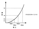
そして、PMOSトランジスタ13の有機エレクトロルミネッセンス素子12とは逆側並びに保持容量15のNMOSトランジスタ14とは逆側は、別々の共通給電線VOエレクトロルミネッセンス1〜VOエレクトロルミネッセンス4に接続されていて、それら共通給電線VOエレクトロルミネッセンス1〜VOエレクトロルミネッセンス4の電圧は、図9に示すように、それらの電圧によって得られる有機エレクトロルミネッセンス素子12の輝度B1〜B4が、
B1:B2:B3:B4=1:2:4:8
となるように設定されている。
【0176】
このような構成であると、各ドット毎に、有機エレクトロルミネッセンス素子12を全て発光させた場合の輝度を15とすると、例えば、配線d0に対応した有機エレクトロルミネッセンス素子12だけを発光させれば輝度は1/15、配線d4に対応した有機エレクトロルミネッセンス素子12だけを発光させれば輝度は8/15、配線d0に対応した有機エレクトロルミネッセンス素子12及び配線d1に対応した有機エレクトロルミネッセンス素子12を発光させれば輝度は3/15、という具合になるから、各ドット毎に16階調が得られることになる。
【0177】
よって、このような階調方式を第3の実施の形態の図7の構成に代えて採用したとしても、その第3の実施の形態と同様の効果が発揮できる。
なお、上述の実施形態において、データ線駆動回路、副データ線駆動回路、走査線駆動回路、及び副走査線駆動回路のそれぞれを、データ線及び走査線が配置された基体内に配置するか、データ線及び走査線が配置された基体と別体にして配置するかについては、仕様等などに対応して適宜選択することができる。また、上記の駆動回路のそれぞれに含まれるトランジスタとしては、シリコンベースのトランジスタ及び薄膜トランジスタのいずれも使用可能であるが、駆動回路をデータ線及び走査線が配置された基体内に配置する場合は、薄膜トランジスタにより駆動回路を構成することが好ましい場合がある。一方、駆動回路をデータ線及び走査線が配置された基体と別体にして配置する場合は、シリコンベースのトランジスタを駆動回路のトランジスタとして用いることが好ましい場合がある。
【0178】
データ線駆動回路、副データ線駆動回路、走査線駆動回路、及び副走査線駆動回路のうちいくつかを一体にしてデータ線または走査線の制御用半導体装置として配置することも可能である。
【0179】
<電子ブック>
先ず、本発明を電子機器である電子ブックに適用した例について説明する。図10に示すように、電子ブック91は、CDROM等の記憶媒体に格納される電子出版に係る書籍などのデータを表示装置の表示画面に表示して読むようにしたものである。
【0180】
この電子ブック91は、ブック形状のフレーム92と、このフレーム92に開閉可能なカバー93とを有している。フレーム92には、その表面に表示面を露出させた状態の表示装置94と、操作部95とが設けられている。
【0181】
この電子ブック91は、表示装置94が上述した有機エレクトロルミネッセンス表示装置10に基づいて構成されており、図示しないドライバにより表示装置94が駆動されるようになされている。
【0182】
<モバイル型コンピュータ>
次に、電子機器であるモバイル型のパーソナルコンピュータに適用した例について説明する。図11は、このパーソナルコンピュータの構成を示す斜視図である。パーソナルコンピュータ100は、図11に示すように、キーボード102を備えた本体部104と、上述した有機エレクトロルミネッセンス表示装置10に基づいて構成された表示装置106とから構成されている。
【0183】
<携帯電話>
次に、電子機器である携帯電話の表示部に適用した例について説明する。図12は、この携帯電話200の構成を示す斜視図である。この携帯電話200は、図12に示すように、複数の操作ボタン202のほか、受話口206、送話口204とともに、上述した有機エレクトロルミネッセンス表示装置10に基づいて構成された表示装置64を備えている。
【0184】
<ディジタルスチルカメラ>
さらに、ファインダに用いたディジタルスチルカメラに適用した例ついて説明する。図13は、このディジタルスチルカメラ300の構成を示す斜視図であるが、外部機器との接続についても簡易的に示すものである。
【0185】
通常のカメラは、被写体の光像によってフィルムを感光するのに対し、ディジタルスチルカメラ300は、被写体の光像をCCD(Charge Coupled Device)などの撮像素子により光電変換して撮像信号を生成するものである。
【0186】
ディジタルスチルカメラ300におけるケース302の背面には、上述した有機エレクトロルミネッセンス表示装置10に基づいて構成された表示装置304が設けられ、CCDによる撮像信号に基づいて、表示を行う構成となっている。このため、表示装置304は、被写体を表示するファインダとして機能する。また、ケース302の観察側(図においては裏面側)には、光学レンズやCCDなどを含んだ受光ユニット306が設けられている。
【0187】
ここで、撮影者が表示装置304に表示された被写体像を確認して、シャッタボタン308を押下すると、その時点におけるCCDの撮像信号が、回路基板310のメモリに転送・格納される。
【0188】
また、このディジタルスチルカメラ300にあっては、ケース302の側面に、ビデオ信号出力端子312と、データ通信用の入出力端子314とが設けられている。そして、図示のように、前者のビデオ信号出力端子312にはテレビモニタ430が、また、後者のデータ通信用の入出力端子314にはパーソナルコンピュータ440が、それぞれ必要に応じて接続される。さらに、所定の操作によって、回路基板310のメモリに格納された撮像信号が、テレビモニタ430や、パーソナルコンピュータ440に出力される構成となっている。
【0189】
なお、電子機器としては、図10の電子ブック91、図11のパーソナルコンピュータ100、図12の携帯電話200、図13のディジタルスチルカメラ300の他にも、液晶テレビや、ビューファインダ型、モニタ直視型のビデオテープレコーダ、カーナビゲーション装置、ページャ、電子手帳、電卓、ワードプロセッサ、ワークステーション、テレビ電話、POS端末、タッチパネルを備えた機器等などが挙げられる。そして、これらの各種電子機器の表示部として、上述した表示装置が適用可能なのは言うまでもない。
【0190】
以上のように、本発明について、複数の実施の形態を挙げて説明した。しかし、本発明は上述の実施の形態に適用されることに限定されるものではない。
【0191】
すなわち、上述の実施の形態では、副データ線駆動回路50には、データ線の一部が選択的に接続されて構成しているが、副データ線駆動回路50には、データ線の全てを接続して構成されていてもよい。
【0192】
また、上述の実施の形態において、データ線駆動回路40及び副データ線駆動回路50は、それぞれ接続されているデータ線に対応した電圧(値)を出力しているが、電流(値)を出力することもできる。
【0193】
また、上述の実施の形態では、副データ線駆動回路50は、キャラクタ表示をする場合について説明しており、具体的には、文字表示、携帯電話における電波強度の表示、日付、カレンダ、デスクトップパターン等、静止画や簡易な表示を行うデータ線の駆動回路や断線等の検査回路或いはプリチャージ回路等として利用できる。
【0194】
さらに、副データ線駆動回路50は、データ線駆動回路40とともに動作させてもよく、副データ線駆動回路50の出力とデータ線駆動回路40の出力を重ね合わせることで、例えば、いわゆるスーパーインポーズ等のような画像処理効果を得ることができる。
【0195】
この場合、例えば、図14中(A)に示すような一画面分の走査線を駆動させるための水平走査信号の出力がなされている場合に、その期間内に、データ線駆動回路40からの出力と、副データ線駆動回路50からの出力とを分ける、具体的には、図14中(B)に示すように、その水平走査期間(水平走査線駆動期間)における、その前半にデータ線駆動回路40からデータ信号▲1▼を出力する一方で、図14中(C)に示すように、その後半に副データ線駆動回路40に切り替えて、この副データ線駆動回路40データからデータ信号▲2▼を出力する。また、この場合、データ信号▲1▼及びデータ信号▲2▼の供給期間(データ線の駆動タイミング)については適宜設定することができ、例えば、この図に示すように、データ信号▲1▼の供給期間をデータ信号▲2▼の供給期間よりも長く設定する。例えば、データ信号▲1▼が画像信号或いは動画信号であり、データ信号▲2▼が簡単な情報からなる場合に、データ信号▲1▼の供給期間をデータ信号▲2▼の供給期間よりも長く設定する。
【0196】
このような構成において、副データ線駆動回路50によりキャラクタ文字表示させると、最初の絵の上にキャラクタ文字表示が重なっているように表示されるようになる。
【0197】
例えば、従来は、オリジナルの画像データ(メモリ上にあるデータ)を直接電気的に加工していたが、上述のように表示することで、そのように加工する場合に比べて構成を極めて簡単にして同等な画像処理効果を得ることができるようになる。
【0198】
なお、データ線駆動回路40と副データ線駆動回路50とによるデータ線X1〜Xnの駆動タイミングについては、水平走査期間内に先に副データ線駆動回路50によりなされるようにしてもよく、或いは前記水平走査期間内にデータ線駆動回路40と副データ線駆動回路50とを交互に動作させてデータ線X1〜Xnを駆動するようにしてもよい。
【0199】
また、上述の実施の形態では、データ線駆動回路40或いは副データ線駆動回路50は、ラッチ回路を含んで構成してもよい。図15には、上述の第1の実施の形態の有機エレクトロルミネッセンス表示装置10が2段として第1及び第2のラッチ回路81,82を備えていている場合のものを示している。
【0200】
このような構成とされた有機エレクトロルミネッセンス表示装置において、デジタルデータは、データ線X1〜Xnに対応した複数のスイッチング素子84、…、84がシフトレジスタ41のシフト動作に同期して順次選択されることで、データ供給線D1〜Dmからパラレル供給される。そして、そのデータは、第1のラッチ回路81にてサンプリングされて、さらに第2のラッチ回路82に転送されてそこでいったんストアされて、D/Aコンバータ回路83を介して、対応する各データ線X1〜Xnに出力される。
【0201】
この有機エレクトロルミネッセンス表示装置10は、データ線X1〜Xnへの出力段にラッチ回路を配置することで、例えば、アドレス線を設けることなく、所望のデータ線を駆動させることができるようになる。
【0202】
また、上述の第1の実施の形態では、副データ線駆動回路50をデコーダ51を設けて構成しているが、デコーダ51に代えて、シフトレジスタを採用することも可能である。シフトレジスタを採用した場合、単色表示モード期間T2でもデータ線X2、X5、X8、…、X(nー1)を順に駆動させることが必要となるが、デコーダ51に比べて配線が簡単で済むから、副データ線駆動回路50によってデータ線を順に駆動させても消費電力がそれほど大きくならない場合、例えば、画素数がそれほど大きくない場合には採用する価値がある。
【0203】
また、上述の第2の実施の形態においても、デコーダ51及び61のいずれか一方或いは両方を、シフトレジスタで置き換えることも可能であり、そのようなシフトレジスタを利用した構成は、上記と同様に副データ線駆動回路50や副走査線駆動回路60によってデータ線や走査線を順に駆動させても消費電力がそれほど大きくならない場合、例えば、画素数がそれほど大きくない場合には採用する価値がある。
【0204】
また、上述の実施の形態では、電気光学装置が有機エレクトロルミネッセンス表示装置である場合について説明している。しかし、これに限定されるものではなく、電気光学装置が、液晶装置や液相分散と電気泳動粒子とを含む泳動分散媒が収容されてなる電気泳動装置であってもよい。要は、本発明が適用された電気光学装置は、格子状に配線された複数のデータ線及び走査線と、データ線と走査線との各交差部に対応して配置された電気光学素子と、を備えた電気光学装置であって、データ線を駆動可能なデータ線駆動回路と、前記データ線駆動回路とは別に前記データ線を駆動可能な副データ線駆動回路と、を備えていることを特徴とするものである。
【0205】
【発明の効果】
以上説明したように、本発明によれば、副データ線駆動回路を設ける構成、若しくは副データ線駆動回路及び副行駆動回路の両方を設ける構成としたため、データ線駆動回路や走査線駆動回路或いは行駆動回路だけで表示制御、断線等の検査或いはプリチャージを行う場合に比べて、消費電力を低減することができるという効果がある。
【0206】
特に、請求項1、7、11、16、17、18、26、30、35、36、37、43、45、50、52、53、54に係る発明であれば、消費電力をより顕著に低減することが可能である。
【図面の簡単な説明】
【図1】本発明の第1の実施の形態を示す回路図である。
【図2】第1の実施の形態の作用を説明するための波形図である。
【図3】有機エレクトロルミネッセンス材料の発光輝度の特性図である。
【図4】有機エレクトロルミネッセンス材料の発光効率の特性図である。
【図5】本発明の第2の実施の形態を示す回路図である。
【図6】本発明の第3の実施の形態の示す回路図である。
【図7】第3の実施の形態の各ドット毎の構成を示す回路図である。
【図8】第3の実施の形態の変形例を示す回路図である。
【図9】図8の構成における各外部電源の電圧と輝度との関係を示す図である。
【図10】本発明の実施の形態の電子機器の例である電子ブックの外観構成を示す斜視図である。
【図11】上記電子機器の例であるコンピュータの外観構成を示す斜視図である。
【図12】上記電子機器の例である携帯電話の外観構成を示す斜視図である。
【図13】上記電子機器の例であるディジタルスチルカメラの外観構成を示す斜視図である。
【図14】データ線駆動回路の出力と副データ線駆動回路の出力とを重ねることの説明に使用した図である。
【図15】上記第1の実施の形態のデータ線駆動回路にラッチ回路を含んだ構成を示す回路図である。
【図16】従来の構成を示す回路図である。
【符号の説明】
10 有機エレクトロルミネッセンス表示装置
20 表示画面
30 走査線駆動回路(行駆動回路)
32 バッファ
33 デコーダ
40 データ線駆動回路
41 シフトレジスタ
42 スイッチング素子
50 副データ線駆動回路
51 デコーダ
52 スイッチング素子
60 副走査線駆動回路(副行駆動回路)
61 デコーダ
62 バッファ
91 電子ブック
100 パーソナルコンピュータ
200 携帯電話
300 デジタルスチルカメラ
X1〜X12 データ線
Y1〜Y7 走査線(行方向配線)[0001]
BACKGROUND OF THE INVENTION
The present invention relates to an electro-optical device and a driving method thereof, an organic electroluminescence display device using an (electroluminescence) element, and an electronic apparatus including the electro-optical device and the organic electroluminescence display device. The power consumption can be reduced.
[0002]
[Prior art]
Examples of the electro-optical device that displays data included in the electronic device include a liquid crystal display device, an electrophoretic device, and an organic electroluminescence display device. The organic electroluminescence display device is configured using an organic electroluminescence element that is an electro-optic element, and FIG. 16 is a diagram illustrating a configuration of a conventional organic
[0003]
That is, the organic
[0004]
The cathode side of each
[0005]
The ends of the scanning lines Y1 and Y2 are connected to the scanning
[0006]
On the other hand, the ends of the data lines X1 to X4 are connected to the data
The output of the
[0007]
The opposite sides of the data lines X1 to X4 of the
[0008]
The shift operation cycle of the
[0009]
With the above configuration, all the scanning lines Y1, Y2,..., Ym are sequentially selected by the shift operation of the
[0010]
[Problems to be solved by the invention]
Even in the conventional organic
[0011]
However, in the conventional organic
[0012]
In other words, in the above conventional configuration, when displaying characters such as characters and symbols, an operation with high power consumption must be performed in the same way as when displaying an image. Since the configuration is such that the scanning lines Y1 to Ym are driven, the configuration consumes unnecessary power.
[0013]
Furthermore, the present invention is not limited to display control, and wasteful power is consumed when disconnection inspection or precharge is performed.
[0014]
The present invention has been made paying attention to such an unsolved problem of the conventional technology, and an electro-optical device that can reduce wasteful power consumption and a driving method thereof, an organic electroluminescence display device, In addition, an object is to provide an electronic device.
[0015]
[Means for Solving the Problems]
In order to achieve the above object, a first electro-optical device according to the present invention corresponds to a plurality of data lines and scanning lines wired in a grid pattern, and each intersection of the data lines and the scanning lines. An electro-optical device comprising: an electro-optical element disposed; a data line driving circuit capable of driving the data line; and a sub data line driving capable of driving the data line separately from the data line driving circuit And a circuit.
[0016]
According to a second electro-optical device of the present invention, in the electro-optical device which is the first electro-optical device of the present invention, the plurality of data lines are connected to the data line driving circuit, and the sub data line driving circuit is connected. Is characterized in that only a part of the plurality of data lines is selectively connected.
[0017]
According to a third electro-optical device of the present invention, in the first or second electro-optical device of the present invention, the sub data line driving circuit includes a decoder.
[0018]
According to a fourth electro-optical device of the present invention, in the first to third electro-optical devices of the present invention, at least one of the data line driving circuit and the sub data line driving circuit includes a shift register. It is characterized by that.
[0019]
According to a fifth electro-optical device of the present invention, in the first to fourth electro-optical devices of the present invention, at least one of the data line driving circuit and the sub data line driving circuit includes a latch circuit. It is characterized by that.
[0020]
According to a sixth electro-optical device of the present invention, in the first to fifth electro-optical devices of the present invention, at least one of the data line driving circuit and the sub data line driving circuit includes a D / A converter circuit. It is characterized by having.
[0021]
According to a seventh electro-optical device of the present invention, in the first to sixth electro-optical devices of the present invention, the sub data line driving circuit is arranged in a specific area of the display screen among the plurality of data lines. It is characterized by selectively connecting only the data lines.
[0022]
According to an eighth electro-optical device of the present invention, in the first to seventh electro-optical devices of the present invention, the electro-optical element capable of red color development, the electro-optical element capable of green color development, and blue color development. Color display is possible by using three dots of the electro-optic element that can be used as one pixel, and the sub data line driving circuit includes data lines corresponding to some of the three colors. It is characterized by only selectively connecting.
[0023]
According to a ninth electro-optical device of the present invention, in the eighth electro-optical device of the present invention, the sub-data line driving circuit includes data lines corresponding to the partial color, and a specific area of the display screen. It is characterized in that only the data lines arranged in are selectively connected.
[0024]
According to a tenth electro-optical device of the present invention, in the first to ninth electro-optical devices of the present invention, switching between the all-dot display mode and the character display mode is possible. Is selected, the data line driving circuit is enabled, and when the character display mode is selected, the sub data line driving circuit is enabled. Yes.
[0025]
According to an eleventh electro-optical device of the present invention, in the first to tenth electro-optical devices of the present invention, the plurality of scanning lines are separate from the scanning line driving circuit capable of driving the plurality of scanning lines and the scanning line driving circuit. A plurality of scanning lines connected to the scanning line driving circuit, and the sub-scanning line driving circuit is connected to the scanning line driving circuit. It is characterized by selectively connecting only a part.
[0026]
According to a twelfth electro-optical device of the present invention, in the eleventh electro-optical device of the present invention, at least one of the scanning line driving circuit and the sub-scanning line driving circuit includes a decoder. Yes.
[0027]
According to a thirteenth electro-optical device of the present invention, in the eleventh or twelfth electro-optical device of the present invention, at least one of the scanning line driving circuit and the sub-scanning line driving circuit includes a shift register. It is characterized by that.
[0028]
A fourteenth electro-optical device according to the present invention is the eleventh to thirteenth electro-optical device according to the present invention, wherein the sub-scanning line driving circuit is arranged in a specific area of the display screen among the plurality of scanning lines. This is characterized in that only the scanning lines are selectively connected.
[0029]
According to a fifteenth electro-optical device of the present invention, in the eleventh to fourteenth electro-optical devices of the present invention, switching is possible between an all-dot display mode and a character display mode. Is selected, the data line driving circuit and the scanning line driving circuit are enabled. When the character display mode is selected, the sub data line driving circuit and the sub scanning line circuit are enabled. It is characterized by becoming.
[0030]
According to a sixteenth electro-optical device of the present invention, in the tenth or fifteenth electro-optical device of the present invention, when the character display mode is selected, the all-dot display mode is selected. In comparison, the feature is that the number of gradations is reduced.
[0031]
According to a seventeenth electro-optical device of the present invention, in the tenth, fifteenth and sixteenth electro-optical devices of the present invention, when the character display mode is selected, the all-dot display mode is selected. Compared to the case where the frame frequency is, the frame frequency is reduced.
[0032]
According to an eighteenth electro-optical device of the present invention, in the tenth, fifteenth, sixteenth, and seventeenth electro-optical devices of the present invention, all the pixels are moved together when the all-dot display mode is shifted to the character display mode. It is characterized in that it can be reset.
[0033]
According to a nineteenth electro-optical device of the present invention, in the first to eighteenth electro-optical devices of the present invention, the data line driving circuit and the sub data line circuit are within a period during which a scanning line for one screen is driven. And the plurality of data lines are driven.
[0034]
In order to achieve the above object, a driving method of the first electro-optical device according to the present invention includes a plurality of data lines and a plurality of scanning lines wired in a lattice shape, the plurality of data lines, and the plurality of data lines. And a data line driving circuit capable of driving the plurality of data lines, and the data lines. The plurality of data lines are driven by switching a sub data line driving circuit capable of driving the plurality of data lines separately from the driving circuit.
[0035]
According to a second electro-optical device driving method of the present invention, in the first electro-optical device driving method of the present invention, the plurality of data lines are connected to the data line driving circuit, and the sub data line driving is performed. Only a part of the plurality of data lines is selectively connected to the circuit.
[0036]
According to a third electro-optical device driving method of the present invention, in the first or second electro-optical device driving method of the present invention, the sub data line driving circuit includes a decoder.
[0037]
According to a fourth electro-optical device driving method of the present invention, in the first to third electro-optical device driving methods of the present invention, at least one of the data line driving circuit and the sub data line driving circuit is: It is characterized by having a shift register.
[0038]
According to a fifth electro-optical device driving method of the present invention, in the first to fourth electro-optical device driving methods of the present invention, at least one of the data line driving circuit and the sub data line driving circuit is: It is characterized by having a latch circuit.
[0039]
According to a sixth electro-optical device driving method of the present invention, in the first to fifth electro-optical device driving methods of the present invention, at least one of the data line driving circuit and the sub data line driving circuit is: A D / A converter circuit is provided.
[0040]
According to a seventh electro-optical device driving method of the present invention, in the first to sixth electro-optical device driving methods of the present invention, the sub data line driving circuit includes a display screen among the plurality of data lines. It is characterized in that only the data lines arranged in the specific area are selectively connected.
[0041]
According to an eighth electro-optical device driving method of the present invention, in the first to seventh electro-optical device driving methods of the present invention, the electro-optical element capable of developing red color, and the electric device capable of generating green color. Color display is possible by using three dots of the optical element and the electro-optical element capable of blue color development as one pixel, and the sub-data line driving circuit includes a part of the three colors. It is characterized in that only data lines corresponding to colors are selectively connected.
[0042]
According to a ninth electro-optical device driving method of the present invention, in the eighth electro-optical device driving method of the present invention, the sub data line driving circuit includes data lines corresponding to the partial colors. This is characterized in that only data lines arranged in a specific area of the display screen are selectively connected.
[0043]
The tenth electro-optical device driving method of the present invention can be switched between the all-dot display mode and the character display mode in the first to ninth electro-optical device driving methods of the present invention. When the all-dot display mode is selected, the data line driving circuit is enabled, and when the character display mode is selected, the sub data line driving circuit is enabled. It is characterized by having.
[0044]
According to an eleventh electro-optical device driving method of the present invention, in the first to tenth electro-optical device driving methods of the present invention, the plurality of scanning lines are connected and the plurality of scanning lines can be driven. A line driving circuit and a sub-scanning line driving circuit that selectively connects only a part of the plurality of scanning lines and can drive the scanning lines separately from the scanning line driving circuit. The plurality of scanning lines are driven.
[0045]
According to a twelfth electro-optical device driving method of the present invention, in the eleventh electro-optical device driving method of the present invention, at least one of the scanning line driving circuit and the sub-scanning line driving circuit includes a decoder. It is characterized by having.
[0046]
According to a thirteenth electro-optical device driving method of the present invention, in the eleventh or twelfth electro-optical device driving method of the present invention, at least one of the scanning line driving circuit and the sub-scanning line driving circuit is It is characterized by having a shift register.
[0047]
According to a fourteenth electro-optical device driving method of the present invention, in the eleventh to thirteenth electro-optical device driving methods of the present invention, the sub-scanning line driving circuit includes a display screen among the plurality of scanning lines. It is characterized in that only the scanning lines arranged in the specific area are selectively connected.
[0048]
The fifteenth electro-optical device driving method of the present invention can switch between the all-dot display mode and the character display mode in the eleventh to fourteenth electro-optical device driving methods of the present invention. When the all-dot display mode is selected, the data line driving circuit and the scanning line driving circuit are enabled, and when the character display mode is selected, the sub data line driving circuit and the scanning line driving circuit are selected. It is characterized in that the sub scanning line circuit becomes effective.
[0049]
According to the sixteenth electro-optical device driving method of the present invention, when the character display mode is selected in the tenth or fifteenth electro-optical device driving method of the present invention, the all-dot display mode is It is characterized in that the number of gradations is reduced as compared with the case where it is selected.
[0050]
According to a seventeenth electro-optical device driving method of the present invention, when the character display mode is selected in the tenth, fifteenth and sixteenth electro-optical device driving methods of the present invention, Compared with the case where the display mode is selected, the frame frequency is reduced.
[0051]
According to an eighteenth electro-optical device driving method of the present invention, the tenth, fifteenth, sixteenth and seventeenth electro-optical device driving methods of the present invention shift from the all-dot display mode to the character display mode. In this case, all pixels can be reset at the same time.
[0052]
According to a nineteenth electro-optical device driving method of the present invention, in the first to eighteenth electro-optical device driving methods of the present invention, the data line driving circuit is driven within a period during which scanning lines for one screen are driven. And the sub data line circuit are switched to drive the data line.
[0053]
In order to achieve the above object, a first organic electroluminescence display device according to the present invention includes a plurality of row-direction wirings and a plurality of data lines arranged in a lattice shape, the plurality of row-direction wirings and a plurality of data lines. An organic electroluminescence element provided corresponding to each intersection of the data lines, a data line driving circuit capable of driving the plurality of data lines, and a row driving circuit capable of driving the plurality of row direction wirings. In the organic electroluminescence display device provided,
In addition to the data line driving circuit, a data line driving sub-data line driving circuit including a decoder is provided, and the data line driving circuit is connected to the plurality of data lines, and the sub-data line Only a part of the plurality of data lines is selectively connected to the drive circuit.
[0054]
The second organic electroluminescence display device of the present invention corresponds to a plurality of row-direction wirings and a plurality of data lines arranged in a lattice pattern, and corresponding intersections of the plurality of row-direction wirings and the plurality of data lines. In the organic electroluminescence display device comprising: the provided organic electroluminescence element; a data line driving circuit capable of driving the plurality of data lines; and a row driving circuit capable of driving the row direction wiring. A sub data line driving circuit for driving a data line including a shift register is provided separately from the driving circuit, and the data line driving circuit is connected to the plurality of data lines, and the sub data line driving circuit is provided. Is characterized in that only a part of the plurality of data lines is selectively connected.
[0055]
According to a third organic electroluminescence display device of the present invention, in the first or second organic electroluminescence display device of the present invention, the data line driving circuit includes a shift register.
[0056]
According to a fourth organic electroluminescence display device of the present invention, in the first to third organic electroluminescence display devices of the present invention, the row driving circuit includes a decoder.
[0057]
According to a fifth organic electroluminescence display device of the present invention, in the first to fourth organic electroluminescence display devices of the present invention, the sub-data line driving circuit may specify a display screen among the plurality of data lines. It is characterized in that only the data lines arranged in the area are selectively connected.
[0058]
According to a sixth organic electroluminescence display device of the present invention, in the first to fifth organic electroluminescence display devices of the present invention, the organic electroluminescence element capable of developing red color, and the organic electroluminescence element capable of developing green color. Color display is possible by using three dots of the luminescence element and the organic electroluminescence element capable of blue color as one pixel, and the sub-data line driving circuit includes a part of the three colors. It is characterized in that only the data lines corresponding to the colors are selectively connected.
[0059]
According to a seventh organic electroluminescence display device of the present invention, in the sixth organic electroluminescence display device of the present invention, the partial color is green.
[0060]
According to an eighth organic electroluminescence display device of the present invention, in the sixth or seventh organic electroluminescence display device of the present invention, the sub data line driving circuit includes data lines corresponding to the part of colors. Thus, only data lines arranged in a specific area of the display screen are selectively connected.
[0061]
According to a ninth organic electroluminescence display device of the present invention, in the first to eighth organic electroluminescence display devices of the present invention, switching is possible between an all-dot display mode and a character display mode. When the all-dot display mode is selected, the data line driving circuit is enabled. When the character display mode is selected, the sub data line driving circuit is enabled. It is characterized by that.
[0062]
According to a tenth organic electroluminescence display device of the present invention, in the first to eighth organic electroluminescence display devices of the present invention, in addition to the row drive circuit, a row direction wiring drive configured including a decoder is provided. A sub-row driving circuit is provided, the plurality of row-direction wirings are connected to the row driving circuit, and only a part of the plurality of row-direction wirings is selectively connected to the sub-row driving circuit. It is characterized by that.
[0063]
An eleventh organic electroluminescence display device according to the present invention is the first to eighth organic electroluminescence display devices according to the present invention, and is for row-direction wiring driving including a shift register separately from the row driving circuit. A plurality of row direction wirings are connected to the row driving circuit, and only a part of the plurality of row direction wirings is selectively connected to the sub row driving circuit. It is characterized by that.
[0064]
According to a twelfth organic electroluminescence display device of the present invention, in the tenth or eleventh organic electroluminescence display device of the present invention, the sub-row driving circuit has a display screen identification among the plurality of row-directional wirings. Only the row-direction wirings arranged in the region are selectively connected.
[0065]
According to a thirteenth organic electroluminescence display device of the present invention, in the eleventh to twelfth organic electroluminescence display devices of the present invention, switching between an all-dot display mode and a character display mode is possible. When the all-dot display mode is selected, the data line driving circuit and the row driving circuit are enabled, and when the character display mode is selected, the sub data line driving circuit and the sub row driving are enabled. It is characterized in that the circuit becomes effective.
[0066]
In the fourteenth organic electroluminescence display device of the present invention, when the character display mode is selected in the ninth or thirteenth organic electroluminescence display device of the present invention, the all-dot display mode is selected. Compared to the case where the number of gradations is, the number of gradations is reduced.
[0067]
In the fifteenth organic electroluminescence display device of the present invention, when the character display mode is selected in the ninth, thirteenth, and fourteenth organic electroluminescence display devices of the present invention, the all-dot display mode is selected. Compared to the case where is selected, the frame frequency is reduced.
[0068]
A sixteenth organic electroluminescence display device according to the present invention is the ninth, thirteenth, fourteenth and fifteenth organic electroluminescence display devices according to the present invention, wherein the character display mode is changed from the all-dot display mode. All pixels can be reset all at once.
[0069]
In order to achieve the above object, the electronic apparatus of the present invention is an electronic apparatus including a display device for displaying data, and the display device includes the first to nineteenth electro-optical devices of the present invention. Alternatively, the electro-optical display device using the first to sixteenth organic electroluminescence display devices of the present invention is used.
[0070]
Here, in the first electro-optical device and the driving method of the electro-optical device according to the invention, in addition to the original data line driving circuit, a sub data line driving circuit is provided, so that the data line driving circuit and the sub optical line driving circuit are connected. A usage mode in which the data line driving circuit is selectively used according to the display form of the data line or the like becomes possible. That is, in addition to the data line driving circuit driven for the original purpose, the sub data line driving circuit is provided with a sub data line driving circuit that can be used for other purposes, for example, a test circuit such as a circuit or a precharge circuit. Is selectively available.
[0071]
In the second electro-optical device and the driving method of the electro-optical device according to the invention, since only a part of the data lines is selectively connected to the sub data line driving circuit, all the data lines Thus, it is possible to use the data line driving circuit when performing display by using the data line driving circuit, and using the sub data line driving circuit when performing display by using some data lines.
[0072]
In the third electro-optical device and the driving method of the electro-optical device according to the present invention, the sub data line driving circuit includes a decoder, so that any of the data lines connected to the sub-data line driving circuit is included. These data lines can be selectively driven.
[0073]
In the fourth electro-optical device and the electro-optical device driving method according to the present invention, at least one of the data line driving circuit and the sub data line driving circuit includes a shift register. In order to operate the data line driving circuit or the sub data line driving circuit including the shift register, it is not necessary to provide many wirings.
[0074]
In the fifth electro-optical device and the electro-optical device driving method according to the present invention, at least one of the data line driving circuit and the sub data line driving circuit includes a latch circuit. For example, a desired data line or scanning line can be driven without providing an address line.
[0075]
According to the sixth electro-optical device and the electro-optical device driving method of the present invention, at least one of the data line driving circuit and the sub data line driving circuit includes a D / A converter circuit. Therefore, for example, it is not necessary to provide a D / A converter circuit in the electro-optical device itself.
[0076]
In the seventh electro-optical device and the electro-optical device driving method according to the present invention, the data line connected to the sub data line driving circuit is a specific area of the screen (the data line extends in the vertical direction of the screen). For example, in the situation where the data line is driven using the sub data line driving circuit, it is a specific area of the screen. It is possible to display only.
[0077]
On the other hand, according to the eighth electro-optical device and the electro-optical device driving method of the present invention, in the situation where the data line is driven using the sub data line driving circuit, display is performed using only a part of the colors. It can be performed.
[0078]
According to the ninth electro-optical device and the electro-optical device driving method of the present invention, in the situation where the data line is driven using the sub data line driving circuit, a part of the color is displayed in the specific area of the screen. Can be displayed using only
[0079]
In the tenth electro-optical device and the driving method of the electro-optical device according to the present invention, the all-dot display mode for outputting an image using all the dots constituting the screen, and relatively simple characters and symbols, etc. When two display modes, a character display mode for displaying a character as a figure, can be selected and the configuration of the eighth electro-optical device of the present invention and the driving method of the electro-optical device is provided. The former can be expressed as a color display mode, and the latter can be expressed as a partial color (single color) display mode.
[0080]
In the tenth electro-optical device and the electro-optical device driving method of the present invention, the all-dot display mode is made to correspond to the original data line driving circuit, and the character display mode is made to correspond to the sub data line driving circuit. Yes. For this reason, in the situation where the all-dot display mode is selected, display is performed using all data lines, and in the situation where the character display mode is selected, display is performed using some data lines. Therefore, the display level of each display mode can be matched with the number of data lines used.
[0081]
Furthermore, in the eleventh electro-optical device and the driving method of the electro-optical device of the present invention, in addition to the original row driving circuit, a sub-row driving circuit is provided, and the sub-row driving circuit includes a row direction. Since only a part of the wiring is selectively connected, the row driving circuit is used when displaying by all the row direction wirings, and the sub-row driving is performed when displaying by a part of the row direction wirings. A usage mode of using a circuit is possible.
[0082]
Furthermore, in the twelfth electro-optical device and the electro-optical device driving method according to the present invention, at least one of the scanning line driving circuit and the sub-scanning line driving circuit includes a decoder. Any scanning line connected to the scanning lines can be selectively driven.
[0083]
In the thirteenth electro-optical device and the electro-optical device driving method according to the present invention, at least one of the scanning line driving circuit and the sub-scanning line driving circuit includes a shift register. In order to operate the scanning line driving circuit and the sub scanning line driving circuit including the shift register, it is not necessary to provide many wirings.
[0084]
In the fourteenth electro-optical device and the driving method of the electro-optical device according to the invention, the scanning line connected to the sub-scanning line driving circuit has a specific area on the screen (the scanning line extends in the horizontal direction of the screen). If the scanning line is extended, for example, the scanning line is arranged in an area such as the upper stage, middle stage, and lower stage of the screen), in the situation where the scanning line is driven using the sub scanning line driving circuit, the screen is specified. Display can be performed only in the area. Therefore, if the fourteenth electro-optical device and the driving method of the electro-optical device according to the present invention has the configuration of the seventh electro-optical device and the driving method of the electro-optical device according to the present invention, the upper left stage of the screen. Further, a finer area such as the upper center stage and the lower right stage can be set as the specific area.
[0085]
In the fifteenth electro-optical device and the electro-optical device driving method of the present invention, the all-dot display mode is made to correspond to the original scanning line driving circuit, and the character display mode is made to correspond to the sub-scanning line driving circuit. Therefore, in the situation where the all-dot display mode is selected, display is performed using all scanning lines, and in the situation where the character display mode is selected, display is performed using some scanning lines. Thus, the display level in each display mode and the number of scanning lines used can be matched.
[0086]
In the sixteenth electro-optical device and the electro-optical device driving method of the present invention, for example, when the character display mode is selected, the number of gradations is set to 2 (that is, each electro-optical device). The device has only two states, colored or not colored.) When the all-dot display mode is selected, the number of gradations is set to 3 or more. .
[0087]
In the seventeenth electro-optical device and the electro-optical device driving method of the present invention, when the character display mode is selected, the frame frequency is reduced, and the scanning line and the data line are selected accordingly. The period (the period during which driving is performed) can be lengthened.
[0088]
Furthermore, in the eighteenth electro-optical device and the driving method of the electro-optical device according to the present invention, since the resetting can be performed all at once, the operation of scanning the entire screen in order to erase the image becomes unnecessary. The extra power consumption consumed when operating the can be suppressed. Further, when characters, symbols, etc. are displayed in the character display mode, it is possible to prevent noise that makes it difficult to distinguish the characters, symbols, etc. from remaining on the screen.
[0089]
According to the nineteenth electro-optical device and the electro-optical device driving method of the present invention, the data line driving circuit and the sub data line circuit are switched within a period in which the scanning lines for one screen are driven. By driving the data line, an image by the data line driving circuit and an image by the sub data line driving circuit can be displayed within a display period in one screen. For example, here, regarding the driving timing of the data line driving circuit and the sub data line driving circuit, the data line is driven by the data line driving circuit in the first half of the scanning line driving period, and the data line is driven by the sub data line driving circuit in the second half. On the contrary, the data line is driven by the sub data line driving circuit in the first half and the data line is driven by the data line driving circuit in the second half.
[0090]
Further, the first organic electroluminescence display device of the present invention has a sub data line driving circuit in addition to the original data line driving circuit, and the sub data line driving circuit includes one of the data lines. Since only part of the data lines are selectively connected, the data line driving circuit is used when displaying with all the data lines, and the sub data line driving circuit is used when displaying with some data lines. The usage mode of, is possible. In addition, since the sub data line driving circuit includes a decoder, any data line among the data lines connected thereto can be selectively driven.
[0091]
Further, even in the second organic electroluminescence display device of the present invention, it has a sub data line driving circuit, and only a part of the data line is selectively connected to the sub data line driving circuit. When the display is performed using all the data lines, the data line driving circuit is used, and when the display is performed using a part of the data lines, the sub data line driving circuit is used. In the second organic electroluminescence display device of the present invention, since the sub data line driving circuit includes a shift register, many wirings are not provided to operate the sub data line driving circuit. You can do it.
[0092]
In the third organic electroluminescence display device of the present invention, since the data line driving circuit includes the shift register, even if the number of data lines driven thereby is large, the data lines It is not necessary to extremely increase the number of wires for operating the drive circuit.
[0093]
In the fourth organic electroluminescence display device of the present invention, since the row driving circuit is constituted by the decoder, only the necessary row direction wiring is driven when the sub data line driving circuit is used. The usage mode is also possible.
[0094]
In the fourth organic electroluminescence display device of the present invention, even when an image is output to the entire screen using the original data line driving circuit, it is necessary to sequentially select and drive the row direction wiring by the decoder. is there. However, since the driving cycle of the row direction wiring is significantly longer than the driving cycle of the data line, even if there are many address selection wirings connected to the decoder, charging and discharging of these address selection wirings Therefore, the power consumption does not become extremely large as the address selection wiring is driven.
[0095]
In the fifth organic electroluminescence display device of the present invention, the data line connected to the sub data line driving circuit is assumed to be a specific area of the screen (the data line extends in the vertical direction of the screen). For example, in the situation where the data lines are driven using the sub data line driving circuit, the display is limited to a specific area of the screen. It can be carried out.
[0096]
On the other hand, in the sixth organic electroluminescence display device of the present invention, in the situation where the data lines are driven using the sub data line driving circuit, display can be performed using only some colors. . In particular, in the seventh organic electroluminescence display device of the present invention, in the situation where the data line is driven using the sub data line driving circuit, the light emitting luminance and the light emitting efficiency are the highest among the currently reported organic EL materials. Display is done with good green (G).
[0097]
In the eighth organic electroluminescence display device of the present invention, in the situation where the data line is driven using the sub data line driving circuit, only a part of the colors is used in the specific area of the screen. Display can be made.
[0098]
In the ninth organic electroluminescence display device of the present invention, an all-dot display mode for outputting an image using all dots constituting the screen and a character that is a relatively simple figure such as a character or a symbol Two display modes, the character display mode to be displayed, can be selected, and when the configuration of the sixth or seventh organic electroluminescence display device of the present invention is provided, the former is a color display mode, and the latter is one. It can also be expressed as a partial color (single color) display mode.
[0099]
In the ninth organic electroluminescence display device of the present invention, the all-dot display mode is made to correspond to the original data line driving circuit, and the character display mode is made to correspond to the sub data line driving circuit. For this reason, in the situation where the all-dot display mode is selected, display is performed using all data lines, and in the situation where the character display mode is selected, display is performed using some data lines. Therefore, the display level of each display mode can be matched with the number of data lines used.
[0100]
Further, the tenth organic electroluminescence display device of the present invention has a sub-row driving circuit in addition to the original row driving circuit, and only a part of the row-direction wiring is included in the sub-row driving circuit. Are selectively connected, the row drive circuit is used when displaying by all row-direction wirings, and the sub-row drive circuit is used when displaying by some row-direction wirings. It is possible to use as follows. In addition, since the sub-row driving circuit is configured to include a decoder, any row-direction wiring among the row-direction wirings connected thereto can be selectively driven.
[0101]
Further, the eleventh organic electroluminescence display device of the present invention also has a sub-row driving circuit, and only a part of the row direction wiring is selectively connected to the sub-row driving circuit. When the display is performed using the row direction wiring, the row driving circuit is used, and when the display is performed using a part of the row direction wiring, the sub-row driving circuit is used. In the eleventh organic electroluminescence display device of the present invention, since the sub-row driving circuit includes a shift register, a large number of wirings are not provided for operating the sub-row driving circuit. It will be over.
[0102]
In the twelfth organic electroluminescence display device of the present invention, the row-direction wiring connected to the sub-row driving circuit has a specific area of the screen (the row-direction wiring extends in the horizontal direction of the screen). Then, for example, the row direction wiring arranged in the upper, middle, and lower areas of the screen), the situation where the row direction wiring is driven using the sub-row driving circuit is limited to a specific area of the screen. Display can be made. Therefore, if the twelfth organic electroluminescence display device of the present invention has the configuration of the fifth organic electroluminescence display device of the present invention, the upper left stage, the upper center stage, the lower right stage of the screen, etc. A finer area can be set as the specific area.
[0103]
In the thirteenth organic electroluminescence display device of the present invention, the all-dot display mode is made to correspond to the original row drive circuit, and the character display mode is made to correspond to the sub-row drive circuit. In the situation where the mode is selected, the display is performed using all the row-direction wirings, and in the situation where the character display mode is selected, the display is performed using a part of the row-direction wirings. Thus, the display level of each display mode can be matched with the number of row-direction wirings used.
[0104]
In the fourteenth organic electroluminescence display device of the present invention, for example, when the character display mode is selected, the number of gradations is 2 (that is, each organic EL element is colored). If the all-dot display mode is selected, the number of gradations can be set to 3 or more.
[0105]
Further, in the fifteenth organic electroluminescence display device of the present invention, when the character display mode is selected, the frame frequency is reduced, and the row period wiring or data line selection period (driven) is reduced accordingly. Can be made longer.
[0106]
Further, in the sixteenth organic electroluminescence display device of the present invention, since it is possible to reset all at once, the operation of scanning the entire screen is unnecessary in order to erase the image. Excessive power consumption can be suppressed. Further, when characters, symbols, etc. are displayed in the character display mode, it is possible to prevent noise that makes it difficult to distinguish the characters, symbols, etc. from remaining on the screen.
[0107]
According to a twentieth electro-optical device driving method of the present invention, the data line is driven by switching between the data line driving circuit and the sub data line driving circuit within one horizontal scanning period. For example, a period in which information having a large number of data such as an image signal is supplied through the data line driving circuit and a period in which character information is supplied through the sub data line driving circuit within one horizontal scanning period are provided. be able to. In this case, it is preferable to set the period for supplying information with a large number of data such as an image signal longer than the period for supplying character information.
[0108]
The electronic apparatus of the present invention is an electronic apparatus provided with a display device for displaying data. As the display device, the first to nineteenth electro-optical devices of the present invention or the first to first of the present invention. By using 16 organic electroluminescence display devices, the above-described effects in the electro-optical device or the organic electroluminescence display device according to the present invention can be obtained.
[0109]
DETAILED DESCRIPTION OF THE INVENTION
Hereinafter, embodiments of the present invention will be described with reference to the drawings.
[0110]
FIG. 1 is a diagram showing a configuration of the first embodiment of the present invention, and is a circuit diagram showing a configuration of an organic
[0111]
That is, even in the organic
[0112]
However, in the present embodiment, the scanning
[0113]
The enable signal EnblX is supplied to the
[0114]
The enable signals EnblX and EnblY are usually low level (logic value “0”) signals. While the low level enable signals EnblX and EnblY are supplied, the
[0115]
While the high-level enable signal EnblX is being generated, the video signal voltages VIDR, VIDG, and VIDB on the
[0116]
The organic
[0117]
The organic
[0118]
The sub data
[0119]
One end of each of the switching
[0120]
The other ends of the switching
[0121]
The basic configuration of the organic
[0122]
In the former color display mode, the scanning
[0123]
In this case, in the color display mode, light emission is controlled by the video signal voltages VIDR, VIDG, and VIDB that are analog voltages, so that, for example, eight levels of gradation are provided for each color. On the other hand, in the monochromatic mode, the light emission is controlled by the character display voltage VCHR that changes in two steps of low level and high level. Therefore, the organic electroluminescence element is colored or colored. There are only two states, that is, the number of gradations is two. As described above, when the monochrome display mode is selected, the number of gradations is reduced as compared with the case where the color display mode is selected.
[0124]
FIG. 2 is a waveform diagram showing the state of each signal of the organic
[0125]
In the color display mode selection period T1, the scanning
[0126]
Further, in the color display mode selection period T1, in synchronization with the drive timing of the scanning lines Y1 to Ym and the data lines X1 to Xn, a video signal voltage VIDR that represents the image data to be displayed as an analog voltage for each pixel and each primary color. VIDG and VIDB are switched at high speed.
[0127]
Therefore, every time the data lines X1 to Xn are driven by the data line driving
[0128]
When shifting from the color display mode selection period T1 to the monochrome display mode period T2, first, the enable signals EnblX and EnblY, which have been at a low level until then, become a high level. Then, the
[0129]
After the time for which the reset operation is guaranteed, the enable signals EnblX and EnblY that were at the high level return to the low level again, and thereafter are fixed at the low level. When the enable signals EnblX and EnblY return to the low level, the
[0130]
Next, the sub data
[0131]
In the monochrome display mode period T2, arbitrary scanning lines Y1 to Ym are driven at arbitrary timing by the
[0132]
In other words, in the single color display mode period T2, only arbitrary dots (however, only G) can be lit, so by displaying any dot according to the shape of the character or symbol or the like to be displayed, A character is output on the
[0133]
As described above, when any dot which is turned off by the
[0134]
Therefore, with the configuration of the present embodiment, when performing character display in the monochromatic display mode period T2, only the necessary scanning lines Y1 to Ym and data lines X2, X5,. Therefore, it is not necessary to wastefully drive scanning lines and data lines wired in areas not related to display, and power consumption can be reduced correspondingly.
[0135]
In addition, if the number of scanning lines and data lines that need to be driven is reduced, the frame frequency can be reduced, and the scanning lines Y1 to Ym and the data lines X2, X5,. Since the selection period of Xn can be lengthened (FIG. 2 shows that the selection period of the scanning line is longer in the monochrome display mode period T2 than in the color display mode period T1). The time required for charging and discharging can be set longer, and the power consumption can be reduced as compared with the case of driving at high speed.
[0136]
Further, in the present embodiment, the character is displayed in a single color (G only) in the single color display mode period T2, and the halftone is not used because the number of gradations is two. Compared with a conventional organic electroluminescence display device that displays characters in full color, power consumption can be greatly reduced.
[0137]
Further, in the monochromatic display mode, green (G) is used. The G light emitting material currently in practical use emits light as shown in FIG. 3 compared to the R light emitting material and the B light emitting material. In addition to being excellent in luminance, it is also excellent in luminous efficiency as shown in FIG. For this reason, in order to obtain the same level of luminance and light emission when displaying a character, the use of the G light emitting material as in the present embodiment is the most compared to the use of other materials. Power consumption can be reduced.
[0138]
As described above, since the power consumption is reduced in various points in the configuration of the present embodiment, the power consumption is significantly reduced as a whole as compared with the conventional organic electroluminescence display device. As a result, the display device is particularly suitable as a display device for an electronic device that requires a slight reduction in power consumption, such as a portable information terminal (mobile phone).
[0139]
FIG. 5 is a circuit diagram showing the configuration of the organic
[0140]
First, the basic configuration of the organic
[0141]
That is, the scanning
[0142]
The
[0143]
The sub-scanning
[0144]
Even in the configuration of this embodiment, in the color display mode period T1, the scanning
[0145]
When shifting to the monochromatic display mode period T2, as in the first embodiment, the enable signals EnblX and EnblY are at a high level, and all the scanning lines Y1 to Ym are driven simultaneously by the
[0146]
Next, after the enable signals EnblX and EnblY return to the low level, the sub scanning
[0147]
Therefore, any one of the scanning lines Y2, Y3, Y5, Y6,... Is driven by the
[0148]
That is, in the monochromatic display mode period T2, only arbitrary dots (only G) arranged in a specific area of the
[0149]
Thus, although there is a difference between the entire area of the
[0150]
In the present embodiment, the scanning
[0151]
Also, with respect to the sub data
[0152]
6 and 7 are diagrams showing a third embodiment of the present invention, and FIG. 6 is a circuit diagram showing a configuration of the organic
[0153]
That is, the organic
[0154]
FIG. 7 is a circuit diagram showing a circuit configuration for causing the
[0155]
The storage part for each bit of the
[0156]
And in this Embodiment, when each of the
S1: S2: S3: S4: S5: S6 = 1: 2: 4: 8: 16: 32
It has become. A current can be supplied to each region of the
[0157]
The
[0158]
Since the write control lines Wi and / Wi are commonly supplied to the respective bits of the
[0159]
Returning to FIG. 6, each write control line Wi, / Wi is connected to a word
[0160]
On the other hand, each of the data lines X1 to Xn is connected to the data line driving
[0161]
Each output of the decoder 45 is the number of bits of digital data k for each dot k (in this example, k = 6) × 3 (where 3 is a number corresponding to the three primary colors R, G, and B constituting the pixel P). Branching output line and the same k × 3 output lines of the
[0162]
When an arbitrary output is selected by the decoder 45, each switching
[0163]
The
[0164]
The enable signal EnblX is supplied to the decoder 45 of the data line driving
[0165]
Also in this embodiment, the sub data
[0166]
In the present embodiment, in the color display mode period T1, the word
[0167]
Here, for example, assuming that a high level signal is 1, a low level signal is 0, a signal of 0 is supplied to the wiring d5, and a signal of 1 is supplied to the other wirings d0 to d4. In the
[0168]
That is, since the ratio of the areas S1 to S6 is set as described above, by appropriately setting digital data to be written to each
[0169]
When shifting to the single color display mode period T2, the enable signals EnblX and EnblY are at a high level and all the image signals are at a high level, as in the first embodiment, so All pixels are reset at once.
[0170]
Next, after the enable signals EnblX and EnblY return to the low level, the sub data
[0171]
Therefore, an arbitrary write control line Wi is selected by the
[0172]
Thus, although there is a difference between the analog data in the first embodiment and the digital data in the third embodiment, the present embodiment is the same as the first embodiment. The following effects can be obtained.
[0173]
In the third embodiment, gradation is given to the light emission amount of each dot by a so-called area gradation method. However, gradation is given to each dot using a plurality of types of external analog voltages. A method can also be adopted.
[0174]
FIG. 8 is a diagram showing an example of the external analog voltage using gradation method, and shows one dot. That is, each dot has a plurality (four in this example) of
[0175]
The side opposite to the
B1: B2: B3: B4 = 1: 2: 4: 8
It is set to become.
[0176]
With such a configuration, assuming that the luminance when all the organic
[0177]
Therefore, even if such a gradation method is adopted instead of the configuration of FIG. 7 of the third embodiment, the same effect as that of the third embodiment can be exhibited.
In the above-described embodiment, each of the data line driving circuit, the sub data line driving circuit, the scanning line driving circuit, and the sub scanning line driving circuit is disposed in the substrate on which the data line and the scanning line are disposed. Whether to arrange the data line and the scanning line separately from the substrate on which the data line and the scanning line are arranged can be appropriately selected in accordance with the specification or the like. In addition, as a transistor included in each of the above driving circuits, any of a silicon-based transistor and a thin film transistor can be used. However, when the driving circuit is disposed in a substrate where data lines and scanning lines are disposed, In some cases, it is preferable to form the driver circuit with a thin film transistor. On the other hand, when the driving circuit is arranged separately from the substrate on which the data lines and the scanning lines are arranged, it may be preferable to use a silicon-based transistor as the transistor of the driving circuit.
[0178]
Some of the data line driving circuit, the sub data line driving circuit, the scanning line driving circuit, and the sub scanning line driving circuit may be integrated as a semiconductor device for controlling data lines or scanning lines.
[0179]
<Electronic book>
First, an example in which the present invention is applied to an electronic book that is an electronic device will be described. As shown in FIG. 10, the
[0180]
The
[0181]
In the
[0182]
<Mobile computer>
Next, an example applied to a mobile personal computer which is an electronic device will be described. FIG. 11 is a perspective view showing the configuration of the personal computer. As shown in FIG. 11, the
[0183]
<Mobile phone>
Next, an example applied to a display unit of a mobile phone that is an electronic device will be described. FIG. 12 is a perspective view showing the configuration of the
[0184]
<Digital still camera>
Further, an example applied to a digital still camera used in a viewfinder will be described. FIG. 13 is a perspective view showing the configuration of the digital
[0185]
An ordinary camera sensitizes a film with a light image of a subject, whereas a digital
[0186]
A
[0187]
Here, when the photographer confirms the subject image displayed on the
[0188]
In the digital
[0189]
In addition to the
[0190]
As described above, the present invention has been described with reference to a plurality of embodiments. However, the present invention is not limited to being applied to the above-described embodiment.
[0191]
In other words, in the above-described embodiment, a part of the data lines is selectively connected to the sub data
[0192]
In the above-described embodiment, the data
[0193]
Further, in the above-described embodiment, the sub data
[0194]
Further, the sub data
[0195]
In this case, for example, when a horizontal scanning signal for driving a scanning line for one screen as shown in FIG. 14A is output, the data
[0196]
In such a configuration, when the character data is displayed by the sub data
[0197]
For example, in the past, original image data (data in the memory) was directly electrically processed, but displaying it as described above makes the configuration extremely simple compared to such processing. Thus, an equivalent image processing effect can be obtained.
[0198]
The driving timing of the data lines X1 to Xn by the data line driving
[0199]
In the above-described embodiment, the data
[0200]
In the organic electroluminescence display device having such a configuration, digital data is sequentially selected by a plurality of switching
[0201]
The organic
[0202]
In the first embodiment described above, the sub data
[0203]
Also in the second embodiment described above, either or both of the
[0204]
In the above-described embodiment, the case where the electro-optical device is an organic electroluminescence display device is described. However, the electro-optical device is not limited to this, and the electro-optical device may be a liquid crystal device or an electrophoretic device in which an electrophoretic dispersion medium including liquid phase dispersion and electrophoretic particles is accommodated. In short, an electro-optical device to which the present invention is applied includes a plurality of data lines and scanning lines wired in a grid pattern, and an electro-optical element disposed corresponding to each intersection of the data lines and the scanning lines. And a data line driving circuit capable of driving a data line, and a sub data line driving circuit capable of driving the data line separately from the data line driving circuit. It is characterized by.
[0205]
【The invention's effect】
As described above, according to the present invention, since the sub data line driving circuit is provided or the sub data line driving circuit and the sub row driving circuit are both provided, the data line driving circuit, the scanning line driving circuit, There is an effect that power consumption can be reduced compared to the case where display control, disconnection inspection, or precharge is performed only by the row drive circuit.
[0206]
In particular, in the invention according to
[Brief description of the drawings]
FIG. 1 is a circuit diagram showing a first embodiment of the present invention.
FIG. 2 is a waveform diagram for explaining the operation of the first embodiment;
FIG. 3 is a characteristic diagram of light emission luminance of an organic electroluminescent material.
FIG. 4 is a characteristic diagram of luminous efficiency of an organic electroluminescent material.
FIG. 5 is a circuit diagram showing a second embodiment of the present invention.
FIG. 6 is a circuit diagram showing a third embodiment of the present invention.
FIG. 7 is a circuit diagram illustrating a configuration for each dot according to a third embodiment;
FIG. 8 is a circuit diagram showing a modification of the third embodiment.
9 is a diagram showing the relationship between the voltage and luminance of each external power supply in the configuration of FIG.
FIG. 10 is a perspective view illustrating an external configuration of an electronic book that is an example of the electronic apparatus according to the embodiment of the invention.
FIG. 11 is a perspective view illustrating an external configuration of a computer that is an example of the electronic apparatus.
FIG. 12 is a perspective view showing an external configuration of a mobile phone as an example of the electronic apparatus.
FIG. 13 is a perspective view illustrating an external configuration of a digital still camera that is an example of the electronic apparatus.
FIG. 14 is a diagram used for explaining the superposition of the output of the data line driving circuit and the output of the sub data line driving circuit;
FIG. 15 is a circuit diagram showing a configuration in which a latch circuit is included in the data line driving circuit of the first embodiment;
FIG. 16 is a circuit diagram showing a conventional configuration.
[Explanation of symbols]
10 Organic electroluminescence display device
20 Display screen
30 Scanning line driving circuit (row driving circuit)
32 buffers
33 Decoder
40 Data line drive circuit
41 Shift register
42 Switching elements
50 Sub data line drive circuit
51 decoder
52 Switching element
60 Sub-scanning line driving circuit (sub-row driving circuit)
61 Decoder
62 buffers
91 ebook
100 Personal computer
200 Mobile phone
300 Digital still camera
X1-X12 data line
Y1 to Y7 scan line (row direction wiring)
Claims (39)
データ線駆動回路、及び副データ線駆動回路を有してなり、
それぞれ異なるデータ線に接続された複数の電気光学素子により画素が構成され、
前記データ線駆動回路は、前記画素を構成する前記複数の電気光学素子のそれぞれに対応するデータ線のすべてに接続され、
前記副データ線駆動回路は、前記画素を構成する前記複数の電気光学素子のうち一部の電気光学素子に対応するデータ線に接続されていることを特徴とする電気光学装置。An electro-optical device comprising: a plurality of data lines and a plurality of scanning lines arranged in a grid pattern; and an electro-optical element disposed corresponding to an intersection of each data line and each scanning line. ,
A data line driving circuit and a sub data line driving circuit;
A pixel is composed of a plurality of electro-optic elements connected to different data lines,
The data line driving circuit is connected to all of the data lines corresponding to each of the plurality of electro-optical elements constituting the pixel,
The electro-optical device, wherein the sub data line driving circuit is connected to a data line corresponding to a part of the electro-optical elements of the plurality of electro-optical elements constituting the pixel.
前記走査線駆動回路には、前記複数の走査線を接続し、前記副走査線駆動回路には、前記複数の走査線のうちの一部のみを選択的に接続したことを特徴とする電気光学装置。10. The electro-optical device according to claim 1, wherein a scanning line driving circuit capable of driving the plurality of scanning lines and a sub-scanning capable of driving the plurality of scanning lines separately from the scanning line driving circuit. Line drive circuit,
The plurality of scanning lines are connected to the scanning line driving circuit, and only some of the plurality of scanning lines are selectively connected to the sub-scanning line driving circuit. apparatus.
前記画素を構成する電気光学素子のそれぞれに対応するデータ線のすべてを駆動可能なデータ線駆動回路と、前記画素を構成する前記複数の電気光学素子のうち一部の電気光学素子に対応するデータ線を駆動可能な副データ線駆動回路とを切り替えて前記複数のデータ線を駆動することを特徴とする電気光学装置の駆動方法。A plurality of data lines and a plurality of scanning lines wired in a grid pattern, and an electro-optical element arranged corresponding to an intersection of each data line and each scanning line, each connected to a different data line A driving method of an electro-optical device in which a pixel is configured by a plurality of electro-optical elements,
A data line driving circuit capable of driving all of the data lines corresponding to each of the electro-optic elements constituting the pixel, and data corresponding to some of the plurality of electro-optic elements constituting the pixel A driving method of an electro-optical device, wherein a plurality of data lines are driven by switching a sub data line driving circuit capable of driving a line.
1水平走査期間内に前記データ線駆動回路と前記副データ線駆動回路とを切り替えて前記複数のデータ線を駆動することを特徴とする電気光学装置の駆動方法。In the driving method of the electro-optical device according to any one of claims 20 to 37,
A driving method of an electro-optical device, wherein the plurality of data lines are driven by switching between the data line driving circuit and the sub data line driving circuit within one horizontal scanning period.
前記表示装置として、請求項1から19のいずれかに記載の電気光学装置を使用したことを特徴とする電子機器。An electronic device having a display device for displaying data,
20. An electronic apparatus using the electro-optical device according to claim 1 as the display device.
Priority Applications (7)
| Application Number | Priority Date | Filing Date | Title |
|---|---|---|---|
| JP2001296479A JP3797174B2 (en) | 2000-09-29 | 2001-09-27 | Electro-optical device, driving method thereof, and electronic apparatus |
| TW090124201A TW525141B (en) | 2000-09-29 | 2001-09-28 | Electro-optical device and method of driving the same, organic electroluminescent display device, and electronic apparatus |
| KR10-2001-0060797A KR100454756B1 (en) | 2000-09-29 | 2001-09-28 | Electro optic apparatus and method of driving the same, organic electroluminescence display device, and electronic equipment |
| CNB01137991XA CN1199142C (en) | 2000-09-29 | 2001-09-28 | Electrooptical device and its drive method, organic electroluminescent display device and electronic device |
| CNB200410063253XA CN100367335C (en) | 2000-09-29 | 2001-09-28 | Electro-optical device and method of driving the same, organic electroluminescent display device, and electronic apparatus |
| US09/964,356 US6867761B2 (en) | 2000-09-29 | 2001-09-28 | Electro-optical device and method of driving the same, organic electroluminescent display device, and electronic apparatus |
| EP01308312A EP1193675A3 (en) | 2000-09-29 | 2001-09-28 | Method for driving an electro-optical device, organic electroluminescent display device, and electronic apparatus |
Applications Claiming Priority (3)
| Application Number | Priority Date | Filing Date | Title |
|---|---|---|---|
| JP2000300934 | 2000-09-29 | ||
| JP2000-300934 | 2000-09-29 | ||
| JP2001296479A JP3797174B2 (en) | 2000-09-29 | 2001-09-27 | Electro-optical device, driving method thereof, and electronic apparatus |
Publications (3)
| Publication Number | Publication Date |
|---|---|
| JP2002175045A JP2002175045A (en) | 2002-06-21 |
| JP2002175045A5 JP2002175045A5 (en) | 2005-02-24 |
| JP3797174B2 true JP3797174B2 (en) | 2006-07-12 |
Family
ID=26601267
Family Applications (1)
| Application Number | Title | Priority Date | Filing Date |
|---|---|---|---|
| JP2001296479A Expired - Fee Related JP3797174B2 (en) | 2000-09-29 | 2001-09-27 | Electro-optical device, driving method thereof, and electronic apparatus |
Country Status (6)
| Country | Link |
|---|---|
| US (1) | US6867761B2 (en) |
| EP (1) | EP1193675A3 (en) |
| JP (1) | JP3797174B2 (en) |
| KR (1) | KR100454756B1 (en) |
| CN (2) | CN1199142C (en) |
| TW (1) | TW525141B (en) |
Families Citing this family (40)
| Publication number | Priority date | Publication date | Assignee | Title |
|---|---|---|---|---|
| TWI282957B (en) | 2000-05-09 | 2007-06-21 | Sharp Kk | Drive circuit, and image display device incorporating the same |
| JP3621347B2 (en) * | 2000-12-27 | 2005-02-16 | シャープ株式会社 | Image display device |
| JP2002170399A (en) * | 2000-12-05 | 2002-06-14 | Fujitsu Ltd | Semiconductor device |
| TW582000B (en) * | 2001-04-20 | 2004-04-01 | Semiconductor Energy Lab | Display device and method of driving a display device |
| JP4011320B2 (en) | 2001-10-01 | 2007-11-21 | 株式会社半導体エネルギー研究所 | Display device and electronic apparatus using the same |
| JP2003271099A (en) * | 2002-03-13 | 2003-09-25 | Semiconductor Energy Lab Co Ltd | Display device and driving method for the display device |
| KR20030086168A (en) * | 2002-05-03 | 2003-11-07 | 엘지.필립스 엘시디 주식회사 | The organic electro-luminescence device and method for fabricating of the same |
| US20030222866A1 (en) * | 2002-05-30 | 2003-12-04 | Eastman Kodak Company | Display driver and method for driving an emissive video display in an image displaying device |
| JP2004077567A (en) | 2002-08-09 | 2004-03-11 | Semiconductor Energy Lab Co Ltd | Display device and driving method therefor |
| TWI359394B (en) * | 2002-11-14 | 2012-03-01 | Semiconductor Energy Lab | Display device and driving method of the same |
| US7271784B2 (en) * | 2002-12-18 | 2007-09-18 | Semiconductor Energy Laboratory Co., Ltd. | Display device and driving method thereof |
| US7159128B2 (en) * | 2003-04-16 | 2007-01-02 | Seiko Epson Corporation | Method and apparatus for selectively reducing the depth of digital data |
| JP3918770B2 (en) | 2003-04-25 | 2007-05-23 | セイコーエプソン株式会社 | Electro-optical device, driving method of electro-optical device, and electronic apparatus |
| JP2005031294A (en) * | 2003-07-10 | 2005-02-03 | Toyota Industries Corp | Display device |
| JP4396814B2 (en) * | 2003-09-01 | 2010-01-13 | セイコーエプソン株式会社 | Capacitance detection device and electronic device |
| JP2005227390A (en) * | 2004-02-10 | 2005-08-25 | Sharp Corp | Driver circuit of display device, and display device |
| KR100583138B1 (en) * | 2004-10-08 | 2006-05-23 | 삼성에스디아이 주식회사 | Light Emitting Display |
| US20060114273A1 (en) * | 2004-11-29 | 2006-06-01 | Sanyo Electric Co., Ltd. | Display panel |
| JP4345743B2 (en) * | 2005-02-14 | 2009-10-14 | セイコーエプソン株式会社 | Electro-optic device |
| JP2007041560A (en) * | 2005-07-04 | 2007-02-15 | Semiconductor Energy Lab Co Ltd | Display device and driving method of the same |
| US20070001954A1 (en) * | 2005-07-04 | 2007-01-04 | Semiconductor Energy Laboratory Co., Ltd. | Display device and driving method of display device |
| EP1758072A3 (en) * | 2005-08-24 | 2007-05-02 | Semiconductor Energy Laboratory Co., Ltd. | Display device and driving method thereof |
| JP5196744B2 (en) * | 2006-06-30 | 2013-05-15 | キヤノン株式会社 | Active matrix display device |
| JP4277055B2 (en) * | 2007-05-29 | 2009-06-10 | シャープ株式会社 | Drive circuit, display device, and television system |
| WO2009107469A1 (en) * | 2008-02-28 | 2009-09-03 | シャープ株式会社 | Drive circuit, and display device |
| JP5604073B2 (en) * | 2009-09-29 | 2014-10-08 | エルジー ディスプレイ カンパニー リミテッド | OLED display device |
| EP2530668A1 (en) * | 2011-05-31 | 2012-12-05 | Siemens Aktiengesellschaft | Flat screen and method for operation |
| TW201322227A (en) * | 2011-11-18 | 2013-06-01 | Au Optronics Corp | Display panel and source driving structure thereof |
| US9064464B2 (en) * | 2012-06-25 | 2015-06-23 | Apple Inc. | Systems and methods for calibrating a display to reduce or eliminate mura artifacts |
| JP6139147B2 (en) * | 2013-01-25 | 2017-05-31 | 三菱電機株式会社 | Display control apparatus, display control method, and program |
| US9754535B2 (en) | 2013-04-02 | 2017-09-05 | Sharp Kabushiki Kaisha | Display device and method for driving display device |
| CN103971634A (en) | 2014-04-18 | 2014-08-06 | 京东方科技集团股份有限公司 | Pixel unit driving circuit, display substrate, display panel and display device |
| WO2016009909A1 (en) * | 2014-07-15 | 2016-01-21 | シャープ株式会社 | Display device and driving method therefor |
| KR102334988B1 (en) * | 2017-09-08 | 2021-12-06 | 엘지디스플레이 주식회사 | Organic light emitting diode display and operation method thereof |
| US11043164B2 (en) * | 2018-01-31 | 2021-06-22 | Ignis Innovation Inc. | Display panel compensation methods |
| CN108447436B (en) * | 2018-03-30 | 2019-08-09 | 京东方科技集团股份有限公司 | Gate driving circuit and its driving method, display device |
| US11062675B2 (en) * | 2019-01-29 | 2021-07-13 | Ignis Innovation Inc. | Compensation for display degradation with temperature normalization |
| US10909905B2 (en) * | 2019-04-02 | 2021-02-02 | Google Llc | Display with switching configurable for power consumption and speed |
| CN113223443B (en) * | 2020-01-17 | 2022-03-18 | 厦门凌阳华芯科技有限公司 | Multi-pixel LED driving chip and LED display screen |
| CN113160763B (en) * | 2020-01-23 | 2022-07-05 | 京东方科技集团股份有限公司 | Touch panel, driving method thereof and display device |
Family Cites Families (25)
| Publication number | Priority date | Publication date | Assignee | Title |
|---|---|---|---|---|
| US4688896A (en) * | 1985-03-04 | 1987-08-25 | General Electric Company | Information conversion device with auxiliary address lines for enhancing manufacturing yield |
| JPH02246481A (en) * | 1989-03-17 | 1990-10-02 | Matsushita Electric Ind Co Ltd | Dot matrix display type television receiver |
| US5168270A (en) | 1990-05-16 | 1992-12-01 | Nippon Telegraph And Telephone Corporation | Liquid crystal display device capable of selecting display definition modes, and driving method therefor |
| DE69123407T2 (en) * | 1990-09-06 | 1997-04-30 | Canon Kk | Electronic device |
| JPH0591447A (en) * | 1991-09-25 | 1993-04-09 | Toshiba Corp | Transmissive liquid crystal display device |
| JPH05210085A (en) * | 1992-01-30 | 1993-08-20 | Canon Inc | Display controller |
| ATE171808T1 (en) * | 1992-07-31 | 1998-10-15 | Canon Kk | DISPLAY CONTROL DEVICE |
| JPH07152340A (en) * | 1993-11-30 | 1995-06-16 | Rohm Co Ltd | Display device |
| US5598565A (en) * | 1993-12-29 | 1997-01-28 | Intel Corporation | Method and apparatus for screen power saving |
| DE69533982T2 (en) * | 1994-11-21 | 2006-01-05 | Seiko Epson Corp. | LIQUID CRYSTAL CONTROL UNIT, LIQUID CRYSTAL DISPLAY UNIT AND LIQUID CRYSTAL CONTROL METHOD |
| CN1146851C (en) | 1995-02-01 | 2004-04-21 | 精工爱普生株式会社 | Liquid crystal display device, method of its driving and methods of its inspection |
| JPH08305323A (en) * | 1995-05-11 | 1996-11-22 | Hitachi Ltd | Liquid crystal display device driving method |
| KR0161918B1 (en) * | 1995-07-04 | 1999-03-20 | 구자홍 | Data driver of liquid crystal device |
| US6329973B1 (en) * | 1995-09-20 | 2001-12-11 | Hitachi, Ltd. | Image display device |
| JPH09146499A (en) * | 1995-11-22 | 1997-06-06 | Toshiba Corp | Information equipment |
| US6697037B1 (en) * | 1996-04-29 | 2004-02-24 | International Business Machines Corporation | TFT LCD active data line repair |
| JP3534948B2 (en) * | 1996-08-09 | 2004-06-07 | 株式会社ルネサステクノロジ | Image display control device |
| US5867140A (en) * | 1996-11-27 | 1999-02-02 | Motorola, Inc. | Display system and circuit therefor |
| JP4147594B2 (en) | 1997-01-29 | 2008-09-10 | セイコーエプソン株式会社 | Active matrix substrate, liquid crystal display device, and electronic device |
| JPH1091088A (en) * | 1997-04-21 | 1998-04-10 | Hitachi Ltd | Matrix display device |
| JPH1074069A (en) * | 1997-07-25 | 1998-03-17 | Toshiba Corp | Color liquid crystal display device |
| GB9803441D0 (en) * | 1998-02-18 | 1998-04-15 | Cambridge Display Tech Ltd | Electroluminescent devices |
| JP3728954B2 (en) * | 1998-12-15 | 2005-12-21 | セイコーエプソン株式会社 | Electro-optical device and electronic apparatus |
| SE516923C2 (en) | 1999-11-25 | 2002-03-26 | Ericsson Telefon Ab L M | The same screen is operated in two modes, which cannot be used simultaneously |
| KR100741904B1 (en) * | 2001-04-16 | 2007-07-24 | 엘지.필립스 엘시디 주식회사 | Liquid crystal display device and method for driving the same |
-
2001
- 2001-09-27 JP JP2001296479A patent/JP3797174B2/en not_active Expired - Fee Related
- 2001-09-28 CN CNB01137991XA patent/CN1199142C/en not_active Expired - Lifetime
- 2001-09-28 US US09/964,356 patent/US6867761B2/en not_active Expired - Lifetime
- 2001-09-28 CN CNB200410063253XA patent/CN100367335C/en not_active Expired - Lifetime
- 2001-09-28 EP EP01308312A patent/EP1193675A3/en not_active Withdrawn
- 2001-09-28 KR KR10-2001-0060797A patent/KR100454756B1/en active IP Right Grant
- 2001-09-28 TW TW090124201A patent/TW525141B/en not_active IP Right Cessation
Also Published As
| Publication number | Publication date |
|---|---|
| KR20020025836A (en) | 2002-04-04 |
| CN1199142C (en) | 2005-04-27 |
| US6867761B2 (en) | 2005-03-15 |
| CN1553425A (en) | 2004-12-08 |
| KR100454756B1 (en) | 2004-11-05 |
| US20020041278A1 (en) | 2002-04-11 |
| EP1193675A3 (en) | 2003-12-03 |
| CN1360294A (en) | 2002-07-24 |
| CN100367335C (en) | 2008-02-06 |
| JP2002175045A (en) | 2002-06-21 |
| TW525141B (en) | 2003-03-21 |
| EP1193675A2 (en) | 2002-04-03 |
Similar Documents
| Publication | Publication Date | Title |
|---|---|---|
| JP3797174B2 (en) | Electro-optical device, driving method thereof, and electronic apparatus | |
| JP6620188B2 (en) | Display device | |
| JP4494214B2 (en) | Display device, electronic equipment | |
| US6788277B2 (en) | Drive unit and drive method of light-emitting display panel | |
| US7502039B2 (en) | Display device and driving method of the same | |
| US6952298B2 (en) | Electro-optical device, method of driving electro-optical device, method of selecting scanning line in electro-optical device, and electronic apparatus | |
| JP2004070293A (en) | Electronic device, method of driving electronic device and electronic equipment | |
| JP2004077567A (en) | Display device and driving method therefor | |
| JP2007025523A (en) | Electronic device, electro-optical device, and electronic apparatus | |
| JP2006309182A (en) | Display and electronic equipment using the same | |
| US7049991B2 (en) | Semiconductor device, digital-analog converter and display device thereof | |
| JP2005331891A (en) | Display apparatus | |
| EP1820180B1 (en) | Display device and electronic apparatus using the same | |
| JP3800401B2 (en) | Image display apparatus and driving method thereof | |
| JP5116202B2 (en) | Driving method of display device | |
| JP2004062163A (en) | Electro-optical device, its driving method and scanning line selection method, and electronic equipment | |
| KR102220960B1 (en) | Pixel circuit reducing static power consumption and driving method thereof | |
| JP4337327B2 (en) | Display and electronic equipment | |
| JP2005326865A (en) | Driving method for electronic apparatus, electronic apparatus, and electronic equipment | |
| JP4467900B2 (en) | Driving method of light emitting device | |
| JP2006011251A (en) | Electro-optical device, its driving method and electronic apparatus | |
| WO2023206231A1 (en) | Scan circuit, display apparatus, and method of operating scan circuit | |
| JP4188000B2 (en) | Semiconductor display device | |
| JPH10312175A (en) | Liquid crystal display device and liquid crystal drive semiconductor device | |
| JP2007219048A (en) | Electrooptical device and electronic equipment |
Legal Events
| Date | Code | Title | Description |
|---|---|---|---|
| A521 | Request for written amendment filed |
Free format text: JAPANESE INTERMEDIATE CODE: A523 Effective date: 20040318 |
|
| A621 | Written request for application examination |
Free format text: JAPANESE INTERMEDIATE CODE: A621 Effective date: 20040318 |
|
| A977 | Report on retrieval |
Free format text: JAPANESE INTERMEDIATE CODE: A971007 Effective date: 20050920 |
|
| A131 | Notification of reasons for refusal |
Free format text: JAPANESE INTERMEDIATE CODE: A131 Effective date: 20051011 |
|
| A521 | Request for written amendment filed |
Free format text: JAPANESE INTERMEDIATE CODE: A523 Effective date: 20051209 |
|
| A131 | Notification of reasons for refusal |
Free format text: JAPANESE INTERMEDIATE CODE: A131 Effective date: 20060117 |
|
| A521 | Request for written amendment filed |
Free format text: JAPANESE INTERMEDIATE CODE: A523 Effective date: 20060302 |
|
| TRDD | Decision of grant or rejection written | ||
| A01 | Written decision to grant a patent or to grant a registration (utility model) |
Free format text: JAPANESE INTERMEDIATE CODE: A01 Effective date: 20060328 |
|
| A61 | First payment of annual fees (during grant procedure) |
Free format text: JAPANESE INTERMEDIATE CODE: A61 Effective date: 20060410 |
|
| R150 | Certificate of patent or registration of utility model |
Free format text: JAPANESE INTERMEDIATE CODE: R150 Ref document number: 3797174 Country of ref document: JP Free format text: JAPANESE INTERMEDIATE CODE: R150 |
|
| FPAY | Renewal fee payment (event date is renewal date of database) |
Free format text: PAYMENT UNTIL: 20090428 Year of fee payment: 3 |
|
| FPAY | Renewal fee payment (event date is renewal date of database) |
Free format text: PAYMENT UNTIL: 20100428 Year of fee payment: 4 |
|
| FPAY | Renewal fee payment (event date is renewal date of database) |
Free format text: PAYMENT UNTIL: 20110428 Year of fee payment: 5 |
|
| FPAY | Renewal fee payment (event date is renewal date of database) |
Free format text: PAYMENT UNTIL: 20110428 Year of fee payment: 5 |
|
| FPAY | Renewal fee payment (event date is renewal date of database) |
Free format text: PAYMENT UNTIL: 20120428 Year of fee payment: 6 |
|
| FPAY | Renewal fee payment (event date is renewal date of database) |
Free format text: PAYMENT UNTIL: 20130428 Year of fee payment: 7 |
|
| FPAY | Renewal fee payment (event date is renewal date of database) |
Free format text: PAYMENT UNTIL: 20130428 Year of fee payment: 7 |
|
| FPAY | Renewal fee payment (event date is renewal date of database) |
Free format text: PAYMENT UNTIL: 20140428 Year of fee payment: 8 |
|
| S111 | Request for change of ownership or part of ownership |
Free format text: JAPANESE INTERMEDIATE CODE: R313113 |
|
| S111 | Request for change of ownership or part of ownership |
Free format text: JAPANESE INTERMEDIATE CODE: R313113 |
|
| R371 | Transfer withdrawn |
Free format text: JAPANESE INTERMEDIATE CODE: R371 |
|
| S111 | Request for change of ownership or part of ownership |
Free format text: JAPANESE INTERMEDIATE CODE: R313113 |
|
| R350 | Written notification of registration of transfer |
Free format text: JAPANESE INTERMEDIATE CODE: R350 |
|
| R250 | Receipt of annual fees |
Free format text: JAPANESE INTERMEDIATE CODE: R250 |
|
| R250 | Receipt of annual fees |
Free format text: JAPANESE INTERMEDIATE CODE: R250 |
|
| R250 | Receipt of annual fees |
Free format text: JAPANESE INTERMEDIATE CODE: R250 |
|
| R250 | Receipt of annual fees |
Free format text: JAPANESE INTERMEDIATE CODE: R250 |
|
| R250 | Receipt of annual fees |
Free format text: JAPANESE INTERMEDIATE CODE: R250 |
|
| LAPS | Cancellation because of no payment of annual fees |