JP5988574B2 - 半導体記憶装置 - Google Patents
半導体記憶装置 Download PDFInfo
- Publication number
- JP5988574B2 JP5988574B2 JP2011281929A JP2011281929A JP5988574B2 JP 5988574 B2 JP5988574 B2 JP 5988574B2 JP 2011281929 A JP2011281929 A JP 2011281929A JP 2011281929 A JP2011281929 A JP 2011281929A JP 5988574 B2 JP5988574 B2 JP 5988574B2
- Authority
- JP
- Japan
- Prior art keywords
- input
- circuit
- power down
- memory cell
- cell array
- Prior art date
- Legal status (The legal status is an assumption and is not a legal conclusion. Google has not performed a legal analysis and makes no representation as to the accuracy of the status listed.)
- Active
Links
Images


Classifications
-
- G—PHYSICS
- G11—INFORMATION STORAGE
- G11C—STATIC STORES
- G11C5/00—Details of stores covered by group G11C11/00
- G11C5/14—Power supply arrangements, e.g. power down, chip selection or deselection, layout of wirings or power grids, or multiple supply levels
-
- G—PHYSICS
- G11—INFORMATION STORAGE
- G11C—STATIC STORES
- G11C5/00—Details of stores covered by group G11C11/00
- G11C5/14—Power supply arrangements, e.g. power down, chip selection or deselection, layout of wirings or power grids, or multiple supply levels
- G11C5/147—Voltage reference generators, voltage or current regulators; Internally lowered supply levels; Compensation for voltage drops
-
- G—PHYSICS
- G11—INFORMATION STORAGE
- G11C—STATIC STORES
- G11C11/00—Digital stores characterised by the use of particular electric or magnetic storage elements; Storage elements therefor
- G11C11/21—Digital stores characterised by the use of particular electric or magnetic storage elements; Storage elements therefor using electric elements
- G11C11/34—Digital stores characterised by the use of particular electric or magnetic storage elements; Storage elements therefor using electric elements using semiconductor devices
- G11C11/40—Digital stores characterised by the use of particular electric or magnetic storage elements; Storage elements therefor using electric elements using semiconductor devices using transistors
- G11C11/401—Digital stores characterised by the use of particular electric or magnetic storage elements; Storage elements therefor using electric elements using semiconductor devices using transistors forming cells needing refreshing or charge regeneration, i.e. dynamic cells
- G11C11/4063—Auxiliary circuits, e.g. for addressing, decoding, driving, writing, sensing or timing
- G11C11/407—Auxiliary circuits, e.g. for addressing, decoding, driving, writing, sensing or timing for memory cells of the field-effect type
- G11C11/4074—Power supply or voltage generation circuits, e.g. bias voltage generators, substrate voltage generators, back-up power, power control circuits
-
- G—PHYSICS
- G11—INFORMATION STORAGE
- G11C—STATIC STORES
- G11C11/00—Digital stores characterised by the use of particular electric or magnetic storage elements; Storage elements therefor
- G11C11/21—Digital stores characterised by the use of particular electric or magnetic storage elements; Storage elements therefor using electric elements
- G11C11/34—Digital stores characterised by the use of particular electric or magnetic storage elements; Storage elements therefor using electric elements using semiconductor devices
- G11C11/40—Digital stores characterised by the use of particular electric or magnetic storage elements; Storage elements therefor using electric elements using semiconductor devices using transistors
- G11C11/401—Digital stores characterised by the use of particular electric or magnetic storage elements; Storage elements therefor using electric elements using semiconductor devices using transistors forming cells needing refreshing or charge regeneration, i.e. dynamic cells
- G11C11/4063—Auxiliary circuits, e.g. for addressing, decoding, driving, writing, sensing or timing
- G11C11/407—Auxiliary circuits, e.g. for addressing, decoding, driving, writing, sensing or timing for memory cells of the field-effect type
- G11C11/409—Read-write [R-W] circuits
- G11C11/4094—Bit-line management or control circuits
-
- G—PHYSICS
- G11—INFORMATION STORAGE
- G11C—STATIC STORES
- G11C11/00—Digital stores characterised by the use of particular electric or magnetic storage elements; Storage elements therefor
- G11C11/21—Digital stores characterised by the use of particular electric or magnetic storage elements; Storage elements therefor using electric elements
- G11C11/34—Digital stores characterised by the use of particular electric or magnetic storage elements; Storage elements therefor using electric elements using semiconductor devices
- G11C11/40—Digital stores characterised by the use of particular electric or magnetic storage elements; Storage elements therefor using electric elements using semiconductor devices using transistors
- G11C11/401—Digital stores characterised by the use of particular electric or magnetic storage elements; Storage elements therefor using electric elements using semiconductor devices using transistors forming cells needing refreshing or charge regeneration, i.e. dynamic cells
- G11C11/4063—Auxiliary circuits, e.g. for addressing, decoding, driving, writing, sensing or timing
- G11C11/407—Auxiliary circuits, e.g. for addressing, decoding, driving, writing, sensing or timing for memory cells of the field-effect type
- G11C11/409—Read-write [R-W] circuits
- G11C11/4097—Bit-line organisation, e.g. bit-line layout, folded bit lines
-
- G—PHYSICS
- G11—INFORMATION STORAGE
- G11C—STATIC STORES
- G11C7/00—Arrangements for writing information into, or reading information out from, a digital store
- G11C7/12—Bit line control circuits, e.g. drivers, boosters, pull-up circuits, pull-down circuits, precharging circuits, equalising circuits, for bit lines
-
- G—PHYSICS
- G11—INFORMATION STORAGE
- G11C—STATIC STORES
- G11C16/00—Erasable programmable read-only memories
- G11C16/02—Erasable programmable read-only memories electrically programmable
- G11C16/06—Auxiliary circuits, e.g. for writing into memory
- G11C16/30—Power supply circuits
-
- G—PHYSICS
- G11—INFORMATION STORAGE
- G11C—STATIC STORES
- G11C2207/00—Indexing scheme relating to arrangements for writing information into, or reading information out from, a digital store
- G11C2207/005—Transfer gates, i.e. gates coupling the sense amplifier output to data lines, I/O lines or global bit lines
-
- G—PHYSICS
- G11—INFORMATION STORAGE
- G11C—STATIC STORES
- G11C2207/00—Indexing scheme relating to arrangements for writing information into, or reading information out from, a digital store
- G11C2207/22—Control and timing of internal memory operations
- G11C2207/2227—Standby or low power modes
Description
なお、電源電圧Vccは、外部電源501とほぼ同一の電圧値を有し(挿入された保護素子や配線による電圧降下などはあるが)、外部電源501を電源として常時供給される電圧である。
以下、本発明の第1の実施形態について、図3を用いて説明する。
当該実施形態による半導体装置は、複数のメモリセルを含むDRAMセルアレイ5と、前記DRAMセルアレイ5と複数のMAI−IO(T/B)8によって接続された周辺回路401と、通常動作時には前記DRAMセルアレイ5及び周辺回路401にそれぞれ動作電圧hVcc,VARAY及びVPERIを供給すると共にパワーダウンモード時にはDeepPowerDown信号によって周辺回路への電源供給を停止することなく前記メモリセルアレイへの動作電圧供給を停止する電源回路501,601とを備えたことを特徴とする。
この構成によって、周辺回路への電源供給をパワーダウンモードによって停止させる大きなトランジスタが不要となり、チップ面積を縮小することが可能となる。
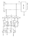
さらに、本願発明者は以下について考察した。上述の第1の実施形態のような構成とした場合、すなわち、周辺回路401へ供給される電圧VPERIをカットせず、常時供給されるようにした場合、ディープパワーダウンモード時のMIO線81及び82とLIO線91及び92との電位差によって、次のような課題も生じる。この課題を、半導体記憶装置におけるメモリセルアレイ及びその周辺回路の基本的な構成の一例を示すブロック図を示した図2を用いて説明する。
図2に示された半導体記憶装置1は、同一構成のメモリセルアレイ5を複数有して構成されている。これらの複数のメモリセルアレイ5は、周辺回路401内のロウデコーダ(XDEC)120、121、…やカラムデコーダ(YDEC)131等に接続されている。
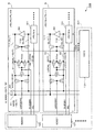
上述のように、通常動作時には、MIO線を“H”レベルにプリチャージし、パワーダウンモード時には、MIO線を“L”レベルにする回路の構成例について図7を参照して説明する。図7に示す回路には、MAIN−IO(T)線81及びMAIN−IO(B)82と、ゲートG1〜G4、G6a、G7〜G8、G9a及びG10と、メインアンプ回路701と、トランジスタT11、T12及びT15〜T17とが含まれている。図7に示す例では、MAIN−IO(T)81及びMAIN−IO(B)82が、メインアンプ回路701に接続されるとともに、トランジスタT11、T12及びT15〜T17が接続されている。この場合、MAIN−IO(T)81は、pチャネルMOSトランジスタT11及びnチャネルMOSトランジスタT15の各ドレインに接続されている。MAIN−IO(T)82は、pチャネルMOSトランジスタT12及びnチャネルMOSトランジスタT16の各ドレインに接続されている。pチャネルMOSトランジスタT11及びT12の各ソースは電源Vccに接続され、nチャネルMOSトランジスタT15及びT16の各ソースはグランドVssに接続されている。また、pチャネルMOSトランジスタT17のドレイン及びソースが、MAIN−IO(T)81又はMAIN−IO(B)82に接続されている。
トランジスタT11のゲートはOR(オア)−NAND(ナンド)複合ゲートG6aの負論理出力に接続されている。トランジスタT15のゲートはNOR(ノア)ゲートG7の負論理出力に接続されている。トランジスタT17のゲートはNANDゲートG8の負論理出力に接続されている。トランジスタT12のゲートはOR−NAND複合ゲートG9aの負論理出力に接続されている。トランジスタT16のゲートはNORゲートG10の負論理出力に接続されている。
NORゲートG2の他方の入力とインバータG3は、LOCAL−IO(T)91及びLOCAL−IO(B)92のプリチャージ時に“H”レベルとなる制御信号FIOが入力される。インバータG3の出力は、NANDゲートG8の他方の入力に接続されている。NORゲートG2の出力は、複合ゲートG6aのAND入力と、複合ゲートG9aのAND入力とに接続されている。
また、書込み時に入力されたデータ、すなわち、リードライトバスRWBS上のデータが、複合ゲートG6aの他方のOR入力と、NORゲートG7の他方の入力と、インバータG4の入力とに入力される。インバータG4の出力が、複合ゲートG9aの他方のOR入力と、NORゲートG10の他方の入力とに接続されている。データ書込み時にはこのリードライトバスRWBS上のデータに基づき、MAIN−IO(T/B)に相補の書き込みデータが生成される。
また、メインアンプを起動する制御信号DAEが、データ読み出し時にメインアンプ回路701に入力され、MAIN−IO(T)81及びMAIN−IO(B)82に読み出された相補のデータに基づいて、メインアンプからデータがリードライトバスRWBSに出力される。なお、MAIN−IO(T)81及びMAIN−IO(B)82は、MAIN−IOプリチャージ信号がLレベルのとき“H”レベル(電源電圧Vcc)にプリチャージされている。
したがって、ディープパワーダウンモード時に、トランジスタT11及びT12がオンしMAIN−IO(T)81及びMAIN−IO(B)82がHレベルにプリチャージされた状態が維持され、一方、LIO線91及び92がグランド電圧Vssとされているため、オフ状態となっているトランジスタT6及びT7を介してリーク電流が流れ、このリーク電流のために、消費電流の低減が制限されないように改良する必要性がある。
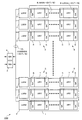
以下、図面を参照して本発明の第2の実施形態としての半導体記憶装置について説明する。図1は、本発明の第2の実施形態としての半導体記憶装置100の主要部の基本的な構成例を示すブロック図である。
101 メモリセル
5 メモリセルアレイ
8 MIO線対
81 MAIN−IO(T)
82 MAIN−IO(B)
9 LIO線対
91 LOCAL−IO(T)
92 LOCAL−IO(B)
T1〜T17 トランジスタ
RWBS リードライトバス
Claims (8)
- 複数のメモリセルを含むメモリセルアレイと、
前記メモリセルアレイと複数の入出力線によって接続された周辺回路と、
前記周辺回路に内部クロック信号を与えるクロック生成回路と、
通常動作時に前記メモリセルアレイおよび前記周辺回路にそれぞれ動作電圧を供給すると共に、前記クロック生成回路によるクロック生成が止まるディープパワーダウンモード中には前記周辺回路への動作電圧の供給を停止することなく前記メモリセルアレイへの動作電圧供給を停止する電源回路と、を備えることを特徴とする半導体記憶装置。 - 前記周辺回路は、前記ディープパワーダウンモード中に前記入出力線を第1レベルにする制御回路を備えることを特徴とする請求項1に記載の半導体記憶装置。
- 前記メモリセルアレイに設けられ、かつ、前記複数のメモリセルに所定のビット線を介して接続されている複数のローカル入出力線であって、前記入出力線と接続されたローカル入出力線と、
前記ディープパワーダウンモード中に、前記入出力線を第1レベルに制御する制御回路と、を備えることを特徴とする請求項1に記載の半導体記憶装置。 - 前記メモリセルアレイに設けられ、かつ、前記複数のメモリセルに所定のビット線を介して接続されている複数のローカル入出力線であって、前記入出力線と接続されたローカル入出力線と、
前記電源回路に接続された第1プリチャージ回路と、を備え、
前記第1プリチャージ回路には、通常動作モード中は前記ローカル入出力線を中間電位へプリチャージするための電位が前記電源回路から供給され、ディープパワーダウンモード中は中間電位とは異なる第2電位が供給されることを特徴とする請求項1に記載の半導体記憶装置。 - 前記周辺回路は、前記ディープパワーダウンモード中に前記入出力線を前記第2電位と同じ電位に設定する制御回路を備えることを特徴とする請求項4に記載の半導体記憶装置。
- 前記制御回路は、前記入出力線を構成する各メイン入出力線とグランドとの間を接続又は非接続状態を確立するよう構成されると共に前記ディープパワーダウンモード中は接続状態となるよう制御されるよう構成されたスイッチング要素の組を含むことを特徴とする請求項2に記載の半導体記憶装置。
- 前記電源回路は、前記ディープパワーダウンモード中に、前記ローカル入出力線に対するプリチャージ電圧の供給を停止する内部電源回路を含むことを特徴とする請求項3に記載の半導体記憶装置。
- 前記周辺回路は、リードコマンド又はライトコマンドの入力に対応して発生する制御信号が活性状態のときに入出力線のプリチャージを停止し、少なくとも前記リードコマンド及びライトコマンドが入力されていないときには入出力線のプリチャージを行なうプリチャージ回路をさらに備え、
前記プリチャージ回路は、ディープパワーダウンモードを示すディープパワーダウンコマンドを受けると前記プリチャージ動作を停止することを特徴とする請求項1から7のいずれか記載の半導体記憶装置。
Priority Applications (3)
| Application Number | Priority Date | Filing Date | Title |
|---|---|---|---|
| JP2011281929A JP5988574B2 (ja) | 2011-12-22 | 2011-12-22 | 半導体記憶装置 |
| US13/712,434 US8861299B2 (en) | 2011-12-22 | 2012-12-12 | Semiconductor memory device |
| US14/487,379 US9208831B2 (en) | 2011-12-22 | 2014-09-16 | Semiconductor memory device |
Applications Claiming Priority (1)
| Application Number | Priority Date | Filing Date | Title |
|---|---|---|---|
| JP2011281929A JP5988574B2 (ja) | 2011-12-22 | 2011-12-22 | 半導体記憶装置 |
Publications (3)
| Publication Number | Publication Date |
|---|---|
| JP2013131278A JP2013131278A (ja) | 2013-07-04 |
| JP2013131278A5 JP2013131278A5 (ja) | 2014-12-18 |
| JP5988574B2 true JP5988574B2 (ja) | 2016-09-07 |
Family
ID=48654408
Family Applications (1)
| Application Number | Title | Priority Date | Filing Date |
|---|---|---|---|
| JP2011281929A Active JP5988574B2 (ja) | 2011-12-22 | 2011-12-22 | 半導体記憶装置 |
Country Status (2)
| Country | Link |
|---|---|
| US (2) | US8861299B2 (ja) |
| JP (1) | JP5988574B2 (ja) |
Families Citing this family (6)
| Publication number | Priority date | Publication date | Assignee | Title |
|---|---|---|---|---|
| JP5988574B2 (ja) * | 2011-12-22 | 2016-09-07 | ピーエスフォー ルクスコ エスエイアールエルPS4 Luxco S.a.r.l. | 半導体記憶装置 |
| US9350324B2 (en) * | 2012-12-27 | 2016-05-24 | Taiwan Semiconductor Manufacturing Co., Ltd. | MCML retention flip-flop/latch for low power applications |
| JP2014149884A (ja) * | 2013-01-31 | 2014-08-21 | Micron Technology Inc | 半導体装置 |
| JP6749021B2 (ja) * | 2015-05-15 | 2020-09-02 | 国立大学法人東北大学 | 抵抗変化型素子を備えた記憶回路 |
| KR102620562B1 (ko) | 2016-08-04 | 2024-01-03 | 삼성전자주식회사 | 비휘발성 메모리 장치 |
| US11017838B2 (en) | 2016-08-04 | 2021-05-25 | Samsung Electronics Co., Ltd. | Nonvolatile memory devices |
Family Cites Families (13)
| Publication number | Priority date | Publication date | Assignee | Title |
|---|---|---|---|---|
| US5940785A (en) * | 1996-04-29 | 1999-08-17 | International Business Machines Corporation | Performance-temperature optimization by cooperatively varying the voltage and frequency of a circuit |
| US5991221A (en) * | 1998-01-30 | 1999-11-23 | Hitachi, Ltd. | Microcomputer and microprocessor having flash memory operable from single external power supply |
| JP2002117673A (ja) | 2000-10-03 | 2002-04-19 | Hitachi Ltd | 半導体記憶装置 |
| JP4827298B2 (ja) * | 2001-01-22 | 2011-11-30 | ルネサスエレクトロニクス株式会社 | 半導体記憶装置 |
| JP4392740B2 (ja) * | 2001-08-30 | 2010-01-06 | 株式会社ルネサステクノロジ | 半導体記憶回路 |
| US6646942B2 (en) * | 2001-10-09 | 2003-11-11 | Micron Technology, Inc. | Method and circuit for adjusting a self-refresh rate to maintain dynamic data at low supply voltages |
| KR100426443B1 (ko) * | 2002-06-29 | 2004-04-13 | 주식회사 하이닉스반도체 | 딥 파워다운 제어 회로 |
| US7031219B2 (en) * | 2004-06-04 | 2006-04-18 | Etron Technology, Inc. | Internal power management scheme for a memory chip in deep power down mode |
| KR100753048B1 (ko) * | 2005-09-05 | 2007-08-30 | 주식회사 하이닉스반도체 | 반도체 메모리 장치의 주변영역 전압 발생 장치 |
| JP2009009680A (ja) * | 2007-05-25 | 2009-01-15 | Nec Electronics Corp | 半導体装置 |
| KR101090469B1 (ko) * | 2009-07-31 | 2011-12-06 | 주식회사 하이닉스반도체 | 데이터제어회로 |
| JP2012038389A (ja) * | 2010-08-09 | 2012-02-23 | Elpida Memory Inc | 半導体装置 |
| JP5988574B2 (ja) * | 2011-12-22 | 2016-09-07 | ピーエスフォー ルクスコ エスエイアールエルPS4 Luxco S.a.r.l. | 半導体記憶装置 |
-
2011
- 2011-12-22 JP JP2011281929A patent/JP5988574B2/ja active Active
-
2012
- 2012-12-12 US US13/712,434 patent/US8861299B2/en active Active
-
2014
- 2014-09-16 US US14/487,379 patent/US9208831B2/en active Active
Also Published As
| Publication number | Publication date |
|---|---|
| US9208831B2 (en) | 2015-12-08 |
| JP2013131278A (ja) | 2013-07-04 |
| US8861299B2 (en) | 2014-10-14 |
| US20130163361A1 (en) | 2013-06-27 |
| US20150003178A1 (en) | 2015-01-01 |
Similar Documents
| Publication | Publication Date | Title |
|---|---|---|
| US7558134B2 (en) | Semiconductor memory device and its operation method | |
| JP5988574B2 (ja) | 半導体記憶装置 | |
| US7158430B2 (en) | Bit line sense amplifier control circuit | |
| JP5595236B2 (ja) | 半導体装置 | |
| JP4221329B2 (ja) | 半導体記憶装置 | |
| JP4987896B2 (ja) | 半導体記憶装置 | |
| US9530459B2 (en) | Semiconductor memory device including a repeater circuit on main data lines | |
| JP2005353172A (ja) | メモリ装置 | |
| JP3667700B2 (ja) | 入力バッファ回路及び半導体記憶装置 | |
| JP5127435B2 (ja) | 半導体記憶装置 | |
| JP2004199759A (ja) | 半導体記憶装置 | |
| JP5144219B2 (ja) | 半導体記憶装置 | |
| JP5980229B2 (ja) | 半導体記憶装置 | |
| US20140028280A1 (en) | Semiconductor device | |
| JP4272592B2 (ja) | 半導体集積回路 | |
| JP2001338490A (ja) | 半導体記憶装置 | |
| JP5776418B2 (ja) | 半導体記憶装置及び半導体記憶装置の制御方法 | |
| JP2008176907A (ja) | 半導体記憶装置 | |
| JP2006004463A (ja) | 半導体記憶装置 | |
| JP2005085455A (ja) | 列読出し増幅器をパワーゲーティングするための方法およびパワーゲーティングされた列読出し増幅器 | |
| KR20140083363A (ko) | 반도체 메모리 장치 | |
| JP5442562B2 (ja) | 半導体記憶装置 | |
| JP2007095264A (ja) | 共有ビットライン感知増幅器構造を有する半導体メモリ素子及びその駆動方法 | |
| JP2008299907A (ja) | 半導体記憶装置 | |
| JPH1196758A (ja) | 半導体記憶装置 |
Legal Events
| Date | Code | Title | Description |
|---|---|---|---|
| A711 | Notification of change in applicant |
Free format text: JAPANESE INTERMEDIATE CODE: A711 Effective date: 20130731 |
|
| A521 | Request for written amendment filed |
Free format text: JAPANESE INTERMEDIATE CODE: A821 Effective date: 20130801 |
|
| A521 | Request for written amendment filed |
Free format text: JAPANESE INTERMEDIATE CODE: A523 Effective date: 20130905 |
|
| RD03 | Notification of appointment of power of attorney |
Free format text: JAPANESE INTERMEDIATE CODE: A7423 Effective date: 20131030 |
|
| RD04 | Notification of resignation of power of attorney |
Free format text: JAPANESE INTERMEDIATE CODE: A7424 Effective date: 20131213 |
|
| A521 | Request for written amendment filed |
Free format text: JAPANESE INTERMEDIATE CODE: A523 Effective date: 20141030 |
|
| A621 | Written request for application examination |
Free format text: JAPANESE INTERMEDIATE CODE: A621 Effective date: 20141030 |
|
| RD03 | Notification of appointment of power of attorney |
Free format text: JAPANESE INTERMEDIATE CODE: A7423 Effective date: 20150327 |
|
| RD04 | Notification of resignation of power of attorney |
Free format text: JAPANESE INTERMEDIATE CODE: A7424 Effective date: 20150331 |
|
| A977 | Report on retrieval |
Free format text: JAPANESE INTERMEDIATE CODE: A971007 Effective date: 20150813 |
|
| A131 | Notification of reasons for refusal |
Free format text: JAPANESE INTERMEDIATE CODE: A131 Effective date: 20150818 |
|
| A601 | Written request for extension of time |
Free format text: JAPANESE INTERMEDIATE CODE: A601 Effective date: 20151111 |
|
| A521 | Request for written amendment filed |
Free format text: JAPANESE INTERMEDIATE CODE: A523 Effective date: 20160212 |
|
| TRDD | Decision of grant or rejection written | ||
| A01 | Written decision to grant a patent or to grant a registration (utility model) |
Free format text: JAPANESE INTERMEDIATE CODE: A01 Effective date: 20160802 |
|
| A61 | First payment of annual fees (during grant procedure) |
Free format text: JAPANESE INTERMEDIATE CODE: A61 Effective date: 20160809 |
|
| R150 | Certificate of patent or registration of utility model |
Ref document number: 5988574 Country of ref document: JP Free format text: JAPANESE INTERMEDIATE CODE: R150 |
|
| S111 | Request for change of ownership or part of ownership |
Free format text: JAPANESE INTERMEDIATE CODE: R313113 |
|
| R350 | Written notification of registration of transfer |
Free format text: JAPANESE INTERMEDIATE CODE: R350 |
|
| S111 | Request for change of ownership or part of ownership |
Free format text: JAPANESE INTERMEDIATE CODE: R313113 |
|
| R360 | Written notification for declining of transfer of rights |
Free format text: JAPANESE INTERMEDIATE CODE: R360 |
|
| R360 | Written notification for declining of transfer of rights |
Free format text: JAPANESE INTERMEDIATE CODE: R360 |
|
| R371 | Transfer withdrawn |
Free format text: JAPANESE INTERMEDIATE CODE: R371 |
|
| S111 | Request for change of ownership or part of ownership |
Free format text: JAPANESE INTERMEDIATE CODE: R313113 |
|
| R350 | Written notification of registration of transfer |
Free format text: JAPANESE INTERMEDIATE CODE: R350 |
|
| R250 | Receipt of annual fees |
Free format text: JAPANESE INTERMEDIATE CODE: R250 |
|
| R250 | Receipt of annual fees |
Free format text: JAPANESE INTERMEDIATE CODE: R250 |
|
| R250 | Receipt of annual fees |
Free format text: JAPANESE INTERMEDIATE CODE: R250 |
|
| R250 | Receipt of annual fees |
Free format text: JAPANESE INTERMEDIATE CODE: R250 |
|
| R250 | Receipt of annual fees |
Free format text: JAPANESE INTERMEDIATE CODE: R250 |