JP5988574B2 - Semiconductor memory device - Google Patents
Semiconductor memory device Download PDFInfo
- Publication number
- JP5988574B2 JP5988574B2 JP2011281929A JP2011281929A JP5988574B2 JP 5988574 B2 JP5988574 B2 JP 5988574B2 JP 2011281929 A JP2011281929 A JP 2011281929A JP 2011281929 A JP2011281929 A JP 2011281929A JP 5988574 B2 JP5988574 B2 JP 5988574B2
- Authority
- JP
- Japan
- Prior art keywords
- input
- circuit
- power down
- memory cell
- cell array
- Prior art date
- Legal status (The legal status is an assumption and is not a legal conclusion. Google has not performed a legal analysis and makes no representation as to the accuracy of the status listed.)
- Active
Links
Images


Classifications
-
- G—PHYSICS
- G11—INFORMATION STORAGE
- G11C—STATIC STORES
- G11C5/00—Details of stores covered by group G11C11/00
- G11C5/14—Power supply arrangements, e.g. power down, chip selection or deselection, layout of wirings or power grids, or multiple supply levels
-
- G—PHYSICS
- G11—INFORMATION STORAGE
- G11C—STATIC STORES
- G11C5/00—Details of stores covered by group G11C11/00
- G11C5/14—Power supply arrangements, e.g. power down, chip selection or deselection, layout of wirings or power grids, or multiple supply levels
- G11C5/147—Voltage reference generators, voltage or current regulators; Internally lowered supply levels; Compensation for voltage drops
-
- G—PHYSICS
- G11—INFORMATION STORAGE
- G11C—STATIC STORES
- G11C11/00—Digital stores characterised by the use of particular electric or magnetic storage elements; Storage elements therefor
- G11C11/21—Digital stores characterised by the use of particular electric or magnetic storage elements; Storage elements therefor using electric elements
- G11C11/34—Digital stores characterised by the use of particular electric or magnetic storage elements; Storage elements therefor using electric elements using semiconductor devices
- G11C11/40—Digital stores characterised by the use of particular electric or magnetic storage elements; Storage elements therefor using electric elements using semiconductor devices using transistors
- G11C11/401—Digital stores characterised by the use of particular electric or magnetic storage elements; Storage elements therefor using electric elements using semiconductor devices using transistors forming cells needing refreshing or charge regeneration, i.e. dynamic cells
- G11C11/4063—Auxiliary circuits, e.g. for addressing, decoding, driving, writing, sensing or timing
- G11C11/407—Auxiliary circuits, e.g. for addressing, decoding, driving, writing, sensing or timing for memory cells of the field-effect type
- G11C11/4074—Power supply or voltage generation circuits, e.g. bias voltage generators, substrate voltage generators, back-up power, power control circuits
-
- G—PHYSICS
- G11—INFORMATION STORAGE
- G11C—STATIC STORES
- G11C11/00—Digital stores characterised by the use of particular electric or magnetic storage elements; Storage elements therefor
- G11C11/21—Digital stores characterised by the use of particular electric or magnetic storage elements; Storage elements therefor using electric elements
- G11C11/34—Digital stores characterised by the use of particular electric or magnetic storage elements; Storage elements therefor using electric elements using semiconductor devices
- G11C11/40—Digital stores characterised by the use of particular electric or magnetic storage elements; Storage elements therefor using electric elements using semiconductor devices using transistors
- G11C11/401—Digital stores characterised by the use of particular electric or magnetic storage elements; Storage elements therefor using electric elements using semiconductor devices using transistors forming cells needing refreshing or charge regeneration, i.e. dynamic cells
- G11C11/4063—Auxiliary circuits, e.g. for addressing, decoding, driving, writing, sensing or timing
- G11C11/407—Auxiliary circuits, e.g. for addressing, decoding, driving, writing, sensing or timing for memory cells of the field-effect type
- G11C11/409—Read-write [R-W] circuits
- G11C11/4094—Bit-line management or control circuits
-
- G—PHYSICS
- G11—INFORMATION STORAGE
- G11C—STATIC STORES
- G11C11/00—Digital stores characterised by the use of particular electric or magnetic storage elements; Storage elements therefor
- G11C11/21—Digital stores characterised by the use of particular electric or magnetic storage elements; Storage elements therefor using electric elements
- G11C11/34—Digital stores characterised by the use of particular electric or magnetic storage elements; Storage elements therefor using electric elements using semiconductor devices
- G11C11/40—Digital stores characterised by the use of particular electric or magnetic storage elements; Storage elements therefor using electric elements using semiconductor devices using transistors
- G11C11/401—Digital stores characterised by the use of particular electric or magnetic storage elements; Storage elements therefor using electric elements using semiconductor devices using transistors forming cells needing refreshing or charge regeneration, i.e. dynamic cells
- G11C11/4063—Auxiliary circuits, e.g. for addressing, decoding, driving, writing, sensing or timing
- G11C11/407—Auxiliary circuits, e.g. for addressing, decoding, driving, writing, sensing or timing for memory cells of the field-effect type
- G11C11/409—Read-write [R-W] circuits
- G11C11/4097—Bit-line organisation, e.g. bit-line layout, folded bit lines
-
- G—PHYSICS
- G11—INFORMATION STORAGE
- G11C—STATIC STORES
- G11C7/00—Arrangements for writing information into, or reading information out from, a digital store
- G11C7/12—Bit line control circuits, e.g. drivers, boosters, pull-up circuits, pull-down circuits, precharging circuits, equalising circuits, for bit lines
-
- G—PHYSICS
- G11—INFORMATION STORAGE
- G11C—STATIC STORES
- G11C16/00—Erasable programmable read-only memories
- G11C16/02—Erasable programmable read-only memories electrically programmable
- G11C16/06—Auxiliary circuits, e.g. for writing into memory
- G11C16/30—Power supply circuits
-
- G—PHYSICS
- G11—INFORMATION STORAGE
- G11C—STATIC STORES
- G11C2207/00—Indexing scheme relating to arrangements for writing information into, or reading information out from, a digital store
- G11C2207/005—Transfer gates, i.e. gates coupling the sense amplifier output to data lines, I/O lines or global bit lines
-
- G—PHYSICS
- G11—INFORMATION STORAGE
- G11C—STATIC STORES
- G11C2207/00—Indexing scheme relating to arrangements for writing information into, or reading information out from, a digital store
- G11C2207/22—Control and timing of internal memory operations
- G11C2207/2227—Standby or low power modes
Description
本発明は、消費電力を低減する際に用いて好適な半導体記憶装置に関する。 The present invention relates to a semiconductor memory device suitable for use in reducing power consumption.
近年、半導体記憶装置においても、消費電力の低減が大きな課題となっており、特にパワーダウン時の消費電力の低減が求められている。そのため、半導体記憶装置をパワーダウンモードとする際、半導体記憶装置への電源の供給を停止したり、クロックを停止することで、消費電力を低減させている。このパワーダウンモードには、半導体記憶装置におけるメモリセルアレイへの電源供給を停止させ、かつクロックも停止させるディープパワーダウン(Deep Power Down;DPD)と呼ばれるモードがある。このディープパワーダウンモードでは、クロック及びクロックイネーブルを除くすべての入力バッファが停止される。また、このディープパワーダウンモードにおいて、半導体記憶装置がDRAM(Dynamic Random Access Memory)の場合には、メモリセルアレイにおける各メモリセルに対するリフレッシュも停止される。したがって、半導体記憶装置がDRAMの場合、メモリセルアレイにおける各メモリセルのデータは、蓄積された電荷の放電のため保持されない。 In recent years, also in semiconductor memory devices, reduction of power consumption has become a major issue, and in particular, reduction of power consumption during power down is required. Therefore, when the semiconductor memory device is set to the power down mode, power consumption is reduced by stopping the supply of power to the semiconductor memory device or stopping the clock. The power down mode includes a mode called deep power down (DPD) in which power supply to the memory cell array in the semiconductor memory device is stopped and the clock is also stopped. In this deep power down mode, all input buffers except the clock and clock enable are stopped. Further, in the deep power down mode, when the semiconductor memory device is a DRAM (Dynamic Random Access Memory), refreshing for each memory cell in the memory cell array is also stopped. Therefore, when the semiconductor memory device is a DRAM, the data of each memory cell in the memory cell array is not retained due to the discharge of accumulated charges.
ここで、図6を参照して、本発明の背景技術について具体的に説明する。図6は、本願出願人において作成した本発明の背景技術を説明するための半導体記憶装置の一例を示したブロック図である。図6(a)は、DRAMセルアレイ内のメインIO線(入出力線;以下、MIO線と称する)とローカルIO線(以下、LIO線と称する)との関係を示すブロック図である。図6(b)は、図6(a)に示した複数のメモリセル(すなわちDRAMセル)101からなるDRAMメモリセルアレイ5とその周辺及び電源回路の関係を示すブロック図である。そして、図6(c)は、図6(b)に示した電源制御回路A801の構成例を示す回路図である。
Here, the background art of the present invention will be specifically described with reference to FIG. FIG. 6 is a block diagram showing an example of a semiconductor memory device for explaining the background art of the present invention created by the applicant of the present application. FIG. 6A is a block diagram showing the relationship between main IO lines (input / output lines; hereinafter referred to as MIO lines) and local IO lines (hereinafter referred to as LIO lines) in the DRAM cell array. FIG. 6B is a block diagram showing the relationship between the DRAM
図6(a)では、メモリセル101に接続されているデータが非反転(T)のローカルIO線であるLOCAL−IO(T)91及びデータが反転(B)のローカルIO線であるLOCAL−IO(B)92がトランジスタ(nチャネルMOS(金属酸化膜半導体)トランジスタ)T6及びT7を介して、データが非反転(T)のメインIO線であるMAIN−IO(T)81及びデータが反転(B)のメインIO線であるMAIN−IO(B)82に接続されている。トランジスタT6及びT7は、図示していないロウデコーダ(XDEC)から出力された制御信号LMIOSWによってオン又はオフ状態に制御される。
In FIG. 6A, LOCAL-IO (T) 91 which is a non-inverted (T) local IO line connected to the
また、図6(b)では、内部電源回路601及び電源制御回路A801に対して、外部電源501から電源が供給される。内部電源回路601は、外部電源501の出力を電源として、メモリセルアレイ5への供給電圧VARYと、プリチャージ用の電圧hVccを出力する。このプリチャージ用の電圧hVccは、例えば、電源電圧Vccの1/2の大きさの電圧である。電源制御回路A801は、外部電源501の出力する電圧を変換し、周辺回路への供給電圧VPERIとして出力する。また、ディープパワーダウン(DEEP POWER DOWN)信号が“H”レベルとなった場合(すなわち、ディープパワーダウンモード時に)、内部電源回路601は電圧VARYと電圧hVccをグランドVssレベルに低下させ(あるいは出力電流を遮断し)、電源制御回路A801は電圧VPERIをグランドVssレベルに低下させる(あるいは出力電流を遮断する)。
なお、電源電圧Vccは、外部電源501とほぼ同一の電圧値を有し(挿入された保護素子や配線による電圧降下などはあるが)、外部電源501を電源として常時供給される電圧である。
In FIG. 6B, power is supplied from the
The power supply voltage Vcc has substantially the same voltage value as that of the external power supply 501 (although there is a voltage drop due to an inserted protective element or wiring), and is a voltage that is constantly supplied using the
メモリセルアレイ5は、図6(a)に示したメモリセル101を複数有して構成されている。周辺回路401は、カラムデコーダ(YDEC)、ロウデコーダ(XDEC)、種々のバッファ回路、コマンドデコーダやアドレスデコーダ等を有して構成されている。メモリセルアレイ5から周辺回路401へはMIO線対8等が配線されている。ここでMIO線対8は、MAIN−IO(T)81及びMAIN−IO(B)82から構成されている。
The
また、図6(b)の電源制御回路A801は、例えば、図6(c)に単純化して示したように、直列に接続されているインバータG21及びG22と、pチャネルMOSトランジスタT21とから構成されている。インバータG21の入力にはディープパワーダウン信号が入力され、インバータG22の出力がトランジスタT21のゲートに接続されている。トランジスタT21のソースは電源Vccに接続され、トランジスタT21のドレインから周辺回路への供給電圧VPERIが出力される。ディープパワーダウン信号が“L”レベルになると、トランジスタT21がオンして電圧VPERIが出力され、ディープパワーダウン信号が“H”レベルになると、トランジスタT21がオフして電圧VPERIの配線に対して、電源電圧Vccの配線とが電気的に非接続となり、電源電圧Vccの配線から電圧VPERIの配線に対して電流が供給されなくなる。
The power supply
図6(b)に示した半導体記憶装置では、ディープパワーダウンモード時に、内部電源回路601及び電源制御回路A801からのVARY(メモリセルアレイへの供給電圧)やhVcc(プリチャージ用の電圧)、及びVPERI(周辺回路への供給電圧)等が、図6(c)の電圧VPERIと同様な構成により供給されなくなる。
In the semiconductor memory device shown in FIG. 6B, in the deep power down mode, VARY (supply voltage to the memory cell array), hVcc (precharge voltage) from the internal
しかしながら、電源制御回路A801は、図6(c)に単純化して記載しているように、例えば、トランジスタからなるスイッチ素子(すなわちトランジスタT21)が必要となる。このスイッチ素子は周辺回路全体として流すべき電流に応じて大きく形成されているため、これを無くすることによって、チップ面積を小さくしたいという要求もある。 However, as described in a simplified manner in FIG. 6C, the power supply control circuit A801 requires, for example, a switch element made of a transistor (that is, the transistor T21). Since this switch element is formed large according to the current to be flowed as the entire peripheral circuit, there is also a demand for reducing the chip area by eliminating this switch element.
上述したように、ディープパワーダウンモード時に、外部電源501あるいは内部電源回路601から、周辺回路401やDRAMセルアレイ5に対する電流の供給を制御する場合、制御のためのスイッチとしてトランジスタを用いる場合、サイズが比較的大きなトランジスタが必要となり、チップ面積が増加してしまうという問題がある。
As described above, when the supply of current from the
上記課題を解決するため、本発明の半導体記憶装置は、複数のメモリセルを含むメモリセルアレイと、メモリセルアレイと複数の入出力線によって接続された周辺回路と、通常動作時にメモリセルアレイ及び周辺回路にそれぞれ動作電圧を供給すると共にパワーダウンモード時には周辺回路への動作電圧の供給を停止することなく前記メモリセルアレイへの動作電圧供給を停止する電源回路とを備えることを特徴とする。 In order to solve the above problems, a semiconductor memory device of the present invention includes a memory cell array including a plurality of memory cells, a peripheral circuit connected to the memory cell array by a plurality of input / output lines, and a memory cell array and a peripheral circuit during normal operation. And a power supply circuit for supplying the operating voltage to the memory cell array without stopping the supply of the operating voltage to the peripheral circuit in the power down mode.
本発明によれば、制御回路によって、メモリセルアレイへの電源及びクロックの供給を停止するパワーダウンモード時に、メモリセルアレイへの動作電圧供給を停止しつつ周辺回路には動作電圧を供給し続けている。したがって、周辺回路へ供給される電圧をオン・オフ制御するための大きな電流を流すための制御回路を省略することができるので、チップ面積を低減することができる。 According to the present invention, in the power down mode in which the supply of power and clocks to the memory cell array is stopped by the control circuit, the operation voltage is continuously supplied to the peripheral circuits while the supply of the operation voltage to the memory cell array is stopped. . Therefore, a control circuit for supplying a large current for on / off control of the voltage supplied to the peripheral circuit can be omitted, so that the chip area can be reduced.
[第1の実施形態]
以下、本発明の第1の実施形態について、図3を用いて説明する。
当該実施形態による半導体装置は、複数のメモリセルを含むDRAMセルアレイ5と、前記DRAMセルアレイ5と複数のMAI−IO(T/B)8によって接続された周辺回路401と、通常動作時には前記DRAMセルアレイ5及び周辺回路401にそれぞれ動作電圧hVcc,VARAY及びVPERIを供給すると共にパワーダウンモード時にはDeepPowerDown信号によって周辺回路への電源供給を停止することなく前記メモリセルアレイへの動作電圧供給を停止する電源回路501,601とを備えたことを特徴とする。
この構成によって、周辺回路への電源供給をパワーダウンモードによって停止させる大きなトランジスタが不要となり、チップ面積を縮小することが可能となる。
さらに、本願発明者は以下について考察した。上述の第1の実施形態のような構成とした場合、すなわち、周辺回路401へ供給される電圧VPERIをカットせず、常時供給されるようにした場合、ディープパワーダウンモード時のMIO線81及び82とLIO線91及び92との電位差によって、次のような課題も生じる。この課題を、半導体記憶装置におけるメモリセルアレイ及びその周辺回路の基本的な構成の一例を示すブロック図を示した図2を用いて説明する。
図2に示された半導体記憶装置1は、同一構成のメモリセルアレイ5を複数有して構成されている。これらの複数のメモリセルアレイ5は、周辺回路401内のロウデコーダ(XDEC)120、121、…やカラムデコーダ(YDEC)131等に接続されている。
[First Embodiment]
Hereinafter, a first embodiment of the present invention will be described with reference to FIG.
The semiconductor device according to the embodiment includes a
With this configuration, a large transistor that stops the power supply to the peripheral circuit in the power down mode is not necessary, and the chip area can be reduced.
Furthermore, the present inventor considered the following. In the case of the configuration as in the first embodiment described above, that is, when the voltage VPERI supplied to the
The
各メモリセルアレイ5は、複数のメモリセル101と、複数のセンスアンプSAと、nチャネルMOSトランジスタT1〜T7とを複数組有して構成されている。複数のメモリセル101は、ロウデコーダ(XDEC)120、121、…に対してワード線WLを介して接続されている。複数のメモリセル101は、また、反転ビット線DL(B)112に接続されるとともに、センスアンプSAを介して非反転ビット線DL(T)111に接続されている。非反転ビット線DL(T)111及び反転ビット線DT(B)112は、スイッチングトランジスタT1及びT2を介して、LOCAL−IO(T)91及びLOCAL−IO(B)92に接続されている。トランジスタT1及びT2は、カラムデコーダ(YDEC)131によって駆動されるカラムアドレス選択線YSWによってオン・オフ制御される。LOCAL−IO(T)91及びLOCAL−IO(B)92は、スイッチングトランジスタT6及びT7を介して、非反転MIO線81及び反転MIO線82に接続されている。トランジスタT6及びT7は、ロウデコーダ(XDEC)120、121、…によって駆動される制御信号LMIOSW0、1、…によってオン・オフ制御される。また、LOCAL−IO(T)91及びLOCAL−IO(B)92間には、トランジスタT3〜T5からなるイコライズ回路が接続されている。この場合、LOCAL−IO(T)91及びLOCAL−IO(B)92間にトランジスタT5のドレイン又はソースが接続され、LOCAL−IO(T)91にトランジスタT3のソースが接続され、そして、LOCAL−IO(B)92にトランジスタT4のソースが接続されている。トランジスタT3及びT4のドレインはプリチャージ用の電圧hVccに接続されている。トランジスタT3〜T5のゲートは、ロウデコーダ(XDEC)120、121、…によって駆動される制御信号DLEQB0、DLWQBE1、…が接続されている。
Each
図2に示すような構成において、MIO線81及び82は、通常“H”レベル(電源電圧Vcc)にプリチャージされており、LOCAL−IO(T)91及びLOCAL−IO(B)92はプリチャージ用電圧hVccによって1/2Vccにプリチャージされている。ただし、ディープパワーダウンモード時には通常、LIO線91及び92はグランド電圧Vssになってしまう。そのため、MAIN−IO(T)81及びMAIN−IO(B)82がVccのままであると、MAIN−IO(T)81及びMAIN−IO(B)82とLOCAL−IO(T)91及びLOCAL−IO(B)92との間に設けられたスイッチングトランジスタT6及びT7等を介して電源VccとグランドVss間に電流(トランジスタT6及びT7はオフ状態であるがリーク電流)が流れてしまう。このため、ディープパワーダウンモード時において、このリーク電流のために、消費電流の低減が制限されるという問題が起こる。 In the configuration shown in FIG. 2, the MIO lines 81 and 82 are normally precharged to the “H” level (power supply voltage Vcc), and the LOCAL-IO (T) 91 and the LOCAL-IO (B) 92 are precharged. Precharged to 1/2 Vcc by the charging voltage hVcc. However, in the deep power down mode, the LIO lines 91 and 92 usually become the ground voltage Vss. Therefore, if MAIN-IO (T) 81 and MAIN-IO (B) 82 remain Vcc, MAIN-IO (T) 81, MAIN-IO (B) 82, LOCAL-IO (T) 91, and LOCAL Current flows between the power supply Vcc and the ground Vss through the switching transistors T6 and T7 provided between the −IO (B) 92 and the like (the transistors T6 and T7 are in the off state but leak current). For this reason, in the deep power down mode, this leakage current causes a problem that reduction of current consumption is limited.
具体的には、メモリセルアレイ0においては、図2に示すように、メモリセル101がアクセスされていないときには、制御信号LMIOSW0は“L”レベル、YSWも“L”レベル、DLEQB0は“H”レベル、MIO線81及び82はVcc、LOCAL−IO(T)91及びLOCAL−IO(B)92は1/2Vcc(hVcc)となっているが、このときディープパワーダウンモードになると、hVccはグランドVssに成るものの、ロウデコーダ(XDEC0)、カラムデコーダ(YDEC)131等の周辺回路104からの制御信号はそのまま維持される。そのため、LOCAL−IO(T)91及びLOCAL−IO(B)線92間に設けられているLIO用イコライズ回路を構成するトランジスタT3及びT4によってLOCAL−IO(T)91及びLOCAL−IO(B)92は共にグランドVSSとなってしまう。この状況は、メモリセルアレイ101のすべてのMIO線81及び82とLIO線91及び92の間で起るため、その電流値は非常に大きなものとなり、パワーダウンしているにもかかわらず、消費電力が減らないという問題が起こる。すなわち、MAIN−IO(T)81及びMAIN−IO(B)82が“H”レベルにプリチャージされている状態で、周辺回路401の電源をオフせずに、メモリセルアレイ5の電源をオフすると、MAIN−IO(T)線81及びMAIN−IO(B)82とLOCAL−IO(T)91及びLOCAL−IO(B)92の間でリーク電流が懸念されるという課題があった。
Specifically, in the
なお、MIO線を“H”レベルにプリチャージする従来技術を開示する文献として特許文献1がある。
上述のように、通常動作時には、MIO線を“H”レベルにプリチャージし、パワーダウンモード時には、MIO線を“L”レベルにする回路の構成例について図7を参照して説明する。図7に示す回路には、MAIN−IO(T)線81及びMAIN−IO(B)82と、ゲートG1〜G4、G6a、G7〜G8、G9a及びG10と、メインアンプ回路701と、トランジスタT11、T12及びT15〜T17とが含まれている。図7に示す例では、MAIN−IO(T)81及びMAIN−IO(B)82が、メインアンプ回路701に接続されるとともに、トランジスタT11、T12及びT15〜T17が接続されている。この場合、MAIN−IO(T)81は、pチャネルMOSトランジスタT11及びnチャネルMOSトランジスタT15の各ドレインに接続されている。MAIN−IO(T)82は、pチャネルMOSトランジスタT12及びnチャネルMOSトランジスタT16の各ドレインに接続されている。pチャネルMOSトランジスタT11及びT12の各ソースは電源Vccに接続され、nチャネルMOSトランジスタT15及びT16の各ソースはグランドVssに接続されている。また、pチャネルMOSトランジスタT17のドレイン及びソースが、MAIN−IO(T)81又はMAIN−IO(B)82に接続されている。
トランジスタT11のゲートはOR(オア)−NAND(ナンド)複合ゲートG6aの負論理出力に接続されている。トランジスタT15のゲートはNOR(ノア)ゲートG7の負論理出力に接続されている。トランジスタT17のゲートはNANDゲートG8の負論理出力に接続されている。トランジスタT12のゲートはOR−NAND複合ゲートG9aの負論理出力に接続されている。トランジスタT16のゲートはNORゲートG10の負論理出力に接続されている。
Incidentally, there is
As described above, a configuration example of a circuit that precharges the MIO line to “H” level during normal operation and sets the MIO line to “L” level in the power-down mode will be described with reference to FIG. The circuit shown in FIG. 7 includes a MAIN-IO (T)
The gate of the transistor T11 is connected to the negative logic output of the OR (Nor) -NAND (Nand) composite gate G6a. The gate of the transistor T15 is connected to the negative logic output of the NOR gate. The gate of the transistor T17 is connected to the negative logic output of the NAND gate G8. The gate of the transistor T12 is connected to the negative logic output of the OR-NAND composite gate G9a. The gate of the transistor T16 is connected to the negative logic output of the NOR gate G10.
また、インバータG1にはライト時(書き込み時)に“H”レベルとなる制御信号WAEが入力される。インバータG1の出力は、NORゲートG2の一方の入力と、複合ゲートG6aの一方のOR入力と、NORゲートG7の一方の入力と、NANDゲートG8の一方の入力と、複合ゲートG9aの一方のOR入力と、NORゲートG10の一方の入力とに接続されている。
NORゲートG2の他方の入力とインバータG3は、LOCAL−IO(T)91及びLOCAL−IO(B)92のプリチャージ時に“H”レベルとなる制御信号FIOが入力される。インバータG3の出力は、NANDゲートG8の他方の入力に接続されている。NORゲートG2の出力は、複合ゲートG6aのAND入力と、複合ゲートG9aのAND入力とに接続されている。
また、書込み時に入力されたデータ、すなわち、リードライトバスRWBS上のデータが、複合ゲートG6aの他方のOR入力と、NORゲートG7の他方の入力と、インバータG4の入力とに入力される。インバータG4の出力が、複合ゲートG9aの他方のOR入力と、NORゲートG10の他方の入力とに接続されている。データ書込み時にはこのリードライトバスRWBS上のデータに基づき、MAIN−IO(T/B)に相補の書き込みデータが生成される。
また、メインアンプを起動する制御信号DAEが、データ読み出し時にメインアンプ回路701に入力され、MAIN−IO(T)81及びMAIN−IO(B)82に読み出された相補のデータに基づいて、メインアンプからデータがリードライトバスRWBSに出力される。なお、MAIN−IO(T)81及びMAIN−IO(B)82は、MAIN−IOプリチャージ信号がLレベルのとき“H”レベル(電源電圧Vcc)にプリチャージされている。
したがって、ディープパワーダウンモード時に、トランジスタT11及びT12がオンしMAIN−IO(T)81及びMAIN−IO(B)82がHレベルにプリチャージされた状態が維持され、一方、LIO線91及び92がグランド電圧Vssとされているため、オフ状態となっているトランジスタT6及びT7を介してリーク電流が流れ、このリーク電流のために、消費電流の低減が制限されないように改良する必要性がある。
Further, a control signal WAE that becomes “H” level at the time of writing (at the time of writing) is input to the inverter G1. The output of inverter G1 is one input of NOR gate G2, one OR input of composite gate G6a, one input of NOR gate G7, one input of NAND gate G8, and one OR input of composite gate G9a. The input is connected to one input of the NOR gate G10.
The other input of the NOR gate G2 and the inverter G3 are supplied with a control signal FIO that becomes “H” level when the LOCAL-IO (T) 91 and the LOCAL-IO (B) 92 are precharged. The output of the inverter G3 is connected to the other input of the NAND gate G8. The output of the NOR gate G2 is connected to the AND input of the composite gate G6a and the AND input of the composite gate G9a.
Further, data input at the time of writing, that is, data on the read / write bus RWBS is input to the other OR input of the composite gate G6a, the other input of the NOR gate G7, and the input of the inverter G4. The output of the inverter G4 is connected to the other OR input of the composite gate G9a and the other input of the NOR gate G10. When writing data, complementary write data is generated in MAIN-IO (T / B) based on the data on the read / write bus RWBS.
Further, a control signal DAE for starting the main amplifier is input to the
Therefore, in the deep power down mode, the transistors T11 and T12 are turned on, and the state in which the MAIN-IO (T) 81 and the MAIN-IO (B) 82 are precharged to the H level is maintained, while the LIO lines 91 and 92 are maintained. Is set to the ground voltage Vss, a leakage current flows through the transistors T6 and T7 in the off state, and it is necessary to improve the leakage current so that reduction of the consumption current is not limited. .
[第2の実施形態]
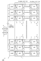
以下、図面を参照して本発明の第2の実施形態としての半導体記憶装置について説明する。図1は、本発明の第2の実施形態としての半導体記憶装置100の主要部の基本的な構成例を示すブロック図である。
[Second Embodiment]
A semiconductor memory device as a second embodiment of the present invention will be described below with reference to the drawings. FIG. 1 is a block diagram showing a basic configuration example of a main part of a
図1に示した半導体記憶装置100は、メモリマット1、複数のローカルアンプ2、ライトアンプ3及びメインアンプ4を含んでいる。メモリマット1は、複数のメモリセルアレイ5を有して構成されている。複数のメモリセルアレイ5は、複数のセンスアンプSAを有するセンスアンプ部6と、複数のメモリセルを有するメモリセルアレイ部7とを含んでいる。各メモリセルアレイ5には、複数のメモリセルアレイ5に対して共通に設けられているMIO線対8と、MIO線対8に対して各メモリセルアレイ5内で接続及び配線されたLIO線対9とが設けられている。
The
複数のローカルアンプ2は、各MIO線対8とコモンIO線対(CIO線対)10との間に設けられていて、各MIO線対8とコモンIO線対10間で入出力される信号を増幅する。ライトアンプ3は、メモリセルアレイ5への書込み用信号を増幅する。メインアンプ4は、コモンIO線対10に出力された読み出し信号を増幅する。
The plurality of
メモリセルアレイ部7から出力された信号はセンスアンプ部6で増幅され、LIO線対9を介してMIO線対8に伝達され、対応するローカルアンプ2で増幅された後にコモンIO線対10を介してメインアンプ4に伝達され、そこで増幅された後に外部に出力される。また、外部から入力された書き込み信号は、ライトアンプ3で増幅された後にコモンIO線対10を介してローカルアンプ2に伝達され、そこで増幅された後に、MIO線対8及びLIO線対9を介してメモリセルアレイ部7に伝達され、入力されたアドレスによって指定された所定のメモリセルに書き込まれる。
The signal output from the memory
なお、本発明の実施の形態は、図1に示した構成に限定されず、例えば、複数のローカルアンプ2を省略して、MIO線対8とCIO線対10とを一体として構成したりすること等が可能である。
The embodiment of the present invention is not limited to the configuration shown in FIG. 1. For example, the plurality of
次に、図2を参照して、本実施形態の半導体記憶装置100における、LIO線用プリチャージ回路を含めた構成としてのメモリセルアレイ5と、周辺回路401の基本的な構成例について説明する。ただし、図2については、上記「背景技術」において説明しているので、ここでは図1に示した各構成と図2に示した各構成との関係について説明する。なお、図1及び図2で対応する構成には同一の符号を用いている。
Next, a basic configuration example of the
図2には、図1に示した構成に加え、周辺回路401として、複数のメモリセルアレイ5に接続されるロウデコーダ(XDEC)120、121、…やカラムデコーダ(YDEC)131等の構成を示している。また、図2のLIO線91及び92の組が、図1のLIO線対9に対応する構成である。なお、図1のローカルアンプ2、ライトアンプ3及びメインアンプ4は、図2の周辺回路401に含まれる構成となる。
2 shows the configuration of row decoders (XDEC) 120, 121,..., Column decoder (YDEC) 131, etc. connected to a plurality of
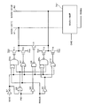
次に、図3を参照して、本実施形態の半導体記憶装置100において、ディープパワーダウン時にMIO線対8のMAIN−IO(T)81及びMAIN−IO(B)82を制御する回路の構成例について説明する。なお、図3において、図6に示したものと同一の構成には同一の符号を用いている。図3(a)は、メモリセルアレイ5内のMAIN−IO(T)81及びMAIN−IO(B)82とLOCAL−IO(T)91及びLOCAL−IO(B)92との関係を示すブロック図である。図3(b)は、図3(a)に示した複数のメモリセル101からなるメモリセルアレイ5とその周辺回路401及び内部電源回路601の関係を示すブロック図である。そして、図3(c)は、本実施形態が特徴とするディープパワーダウン時にMAIN−IO(T)81及びMAIN−IO(B)82を制御する回路の構成例を示した回路図である。
Next, referring to FIG. 3, in the
図3(a)では、メモリセル101に接続されている非反転及び反転LIO線91及び92がトランジスタT6及びT7を介して、MAIN−IO(T)81及びMAIN−IO(B)82に接続されている。トランジスタT6及びT7は、図2のロウデコーダ120、121、…等から出力された制御信号LMIOSW(すなわち図2のLMIOSW0、LMIOSW1、…)によってオン・オフ制御される。
In FIG. 3A, non-inverted and inverted
また、図3(b)では、内部電源回路601に対して、外部電源501から電源が供給される。内部電源回路601は、外部電源501の出力を電源として、メモリセルアレイ5への供給電圧VARYと、プリチャージ用の電圧hVccを出力する。このプリチャージ用の電圧hVccは、例えば、電源電圧Vccの1/2の大きさの電圧である。また、ディープパワーダウン信号が“H”レベルとなった場合、内部電源回路601は電圧VARYと電圧hVccをグランドVssレベルに低下させる(あるいは出力電流を遮断する)。また、本実施形態では、図6の電源制御回路A801は省略され、外部電源501の出力が、そのまま電圧VPERIとして周辺回路401へ入力される。
In FIG. 3B, power is supplied from the
また、図3(b)に示したように、本実施形態では、電源制御回路A801が省略されている。そして、図3(c)に示すように、新たに追加される構成として、ディープパワーダウン信号が“H”レベルとなった場合にMIO線対8をグランドVssのレベルに変化させる(及び維持する)1対のnチャネルMOSトランジスタT13及びT14が設けられている。ここで、トランジスタT13は、MAIN−IO(T)線81にドレインが接続され、グランドVssにソースが接続され、そして、ディープパワーダウン信号がゲートに入力されている。また、トランジスタT14は、MAIN−IO(B)線82にドレインが接続され、グランドVssにソースが接続され、そして、ディープパワーダウン信号がゲートに入力されている。これらのトランジスタT13及びT14は、例えば周辺回路401内に設けることができる。
Further, as shown in FIG. 3B, the power supply control circuit A801 is omitted in this embodiment. Then, as shown in FIG. 3C, as a newly added configuration, the
なお、MIO線対8には、MIO線対8をプリチャージする際に、MIO線対8を電源Vccに接続する1対のpチャネルMOSトランジスタT18及びT19が接続されている。ここで、トランジスタT18は、MAIN−IO(T)線81にドレインが接続され、電源Vccにソースが接続され、そして、MIO線をプリチャージする際に“L”レベルとなる制御信号(MAIN−IOプリチャージ信号)がゲートに入力されている。また、トランジスタT19は、MAIN−IO(B)線82にドレインが接続され、電源Vccにソースが接続され、そして、MIO線をプリチャージする際に“L”レベルとなる制御信号がゲートに入力されている。これらのトランジスタT18及びT19は、ディープパワーダウンモード時にはオフに制御され、MIO線対9には電源Vccが供給されない。
The
図3(b)に示した半導体記憶装置100では、ディープパワーダウンモード時に、内部電源回路601からのVARY(メモリセルアレイへの供給電圧)やhVcc(プリチャージ用の電圧)がカットされVssとされる。また、ディープパワーダウンモード時に、LIO線対9がグランドVssのレベルに制御される。
In the
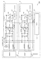
次に、図4を参照して、MAIN−IO(T)81及びMAIN−IO(B)82をプリチャージする回路の構成例について説明する。ただし、図4に示した例は、図1を参照して説明したローカルアンプ2とCIO線対10とを省略した構成に対応させたものとしている。図4に示した回路は、図7を参照して説明した回路と比較して次の点が異なっている。また、図7の複合ゲートG6a及びG9aに代えて、複合ゲートG6及びG9が設けられているとともに、MAIN−IO(T)及びMAIN−IO(B)82に図3(c)を参照して説明したトランジスタT13及びT14が接続されている。図4に示す回路には、MAIN−IO(T)81及びMAIN−IO(B)82と、ゲートG1=G10と、メインアンプ回路701と、トランジスタT11〜T17とが含まれている。なお、図4に示した構成例では、トランジスタT11、T12及びT17が、図3(c)に示したトランジスタT18及びT19に対応する構成である。また、図4におけるゲートG6、G8及びG9の出力信号が、図3(c)に示したMAIN−IOプリチャージ信号に対応する制御信号である。
Next, a configuration example of a circuit for precharging MAIN-IO (T) 81 and MAIN-IO (B) 82 will be described with reference to FIG. However, the example shown in FIG. 4 corresponds to the configuration in which the
すなわち、図3に示す例では、MAIN−IO(T)81及びMAIN−IO(B)82には、メインアンプ回路701に接続されるとともに、トランジスタT11〜T17が接続されている。この場合、MAIN−IO(T)81は、pチャネルMOSトランジスタT11及びnチャネルMOSトランジスタT15の各ドレインに接続されている。MAIN−IO(T)81は、さらに、nチャネルMOSトランジスタT13のドレインに接続されている。MAIN−IO(B)82は、pチャネルMOSトランジスタT12及びnチャネルMOSトランジスタT16の各ドレインに接続されている。MAIN−IO(B)82は、さらに、nチャネルMOSトランジスタT14のドレインに接続されている。pチャネルMOSトランジスタT11及びT12の各ソースは電源Vccに接続され、nチャネルMOSトランジスタT15及びT16の各ソースはグランドVssに接続されている。また、nチャネルMOSトランジスタT13及びT14の各ソースはグランドVssに接続されている。また、pチャネルMOSトランジスタT17のドレイン及びソースが、MAIN−IO(T)81又はMAIN−IO(B)82に接続されている。
In other words, in the example shown in FIG. 3, the MAIN-IO (T) 81 and the MAIN-IO (B) 82 are connected to the
トランジスタT11のゲートはOR−NAND複合ゲートG6の負論理出力に接続されている。トランジスタT15のゲートはNORゲートG7の負論理出力に接続されている。トランジスタT17のゲートはNANDゲートG8の負論理出力に接続されている。トランジスタT12のゲートはOR−NAND複合ゲートG9の負論理出力に接続されている。トランジスタT16のゲートはNORゲートG10の負論理出力に接続されている。トランジスタT13及びT14のゲートには、ディープパワーダウン信号が入力される。 The gate of the transistor T11 is connected to the negative logic output of the OR-NAND composite gate G6. The gate of the transistor T15 is connected to the negative logic output of the NOR gate G7. The gate of the transistor T17 is connected to the negative logic output of the NAND gate G8. The gate of the transistor T12 is connected to the negative logic output of the OR-NAND composite gate G9. The gate of the transistor T16 is connected to the negative logic output of the NOR gate G10. A deep power down signal is input to the gates of the transistors T13 and T14.
また、インバータG1にはライト時(書き込み時)に“H”レベルとなる制御信号WAEが入力される。インバータG1の出力は、NORゲートG2の一方の入力と、複合ゲートG6の一方のOR入力と、NORゲートG7の一方の入力と、NANDゲートG8の一方の入力と、複合ゲートG9の一方のOR入力と、NORゲートG10の一方の入力とに接続されている。 Further, a control signal WAE that becomes “H” level at the time of writing (at the time of writing) is input to the inverter G1. The output of inverter G1 is one input of NOR gate G2, one OR input of composite gate G6, one input of NOR gate G7, one input of NAND gate G8, and one OR input of composite gate G9. The input is connected to one input of the NOR gate G10.
NORゲートG2の他方の入力とインバータG3には、LOCAL−IO(T)91及びLOCAL−IO(B)92のプリチャージ時に“H”レベルとなる制御信号FIOが入力される。インバータG3の出力は、NANDゲートG8の他方の入力に接続されている。NORゲートG2の出力は、複合ゲートG6の一方のAND入力と、複合ゲートG9の一方のAND入力とに接続されている。 The other input of the NOR gate G2 and the inverter G3 are supplied with a control signal FIO that becomes “H” level when the LOCAL-IO (T) 91 and the LOCAL-IO (B) 92 are precharged. The output of the inverter G3 is connected to the other input of the NAND gate G8. The output of the NOR gate G2 is connected to one AND input of the composite gate G6 and one AND input of the composite gate G9.
また、リードライトバスRWBS上のデータが、複合ゲートG6の他方のOR入力と、NORゲートG7の他方の入力と、インバータG4の入力とに入力される。インバータG4の出力が、複合ゲートG9の他方のOR入力と、NORゲートG10の他方の入力とに接続されている。データ書込み時にはリードライトバスRWBS上のデータに基づき、相補の書込みデータが生成されMAIN−IO(T/B)に出力され、詳述はしないがLOCAL−IOを介してメモリにデータが書き込まれる。 Data on the read / write bus RWBS is input to the other OR input of the composite gate G6, the other input of the NOR gate G7, and the input of the inverter G4. The output of the inverter G4 is connected to the other OR input of the composite gate G9 and the other input of the NOR gate G10. At the time of data writing, complementary write data is generated based on the data on the read / write bus RWBS and output to the MAIN-IO (T / B). Although not described in detail, the data is written to the memory via the LOCAL-IO.
また、インバータG5にはディープパワーダウンモード時に“H”レベルとなる制御信号DPDが入力される。インバータG5の出力は、複合ゲートG6の他方のAND入力と、複合ゲートG9の他方のAND入力とに接続されている。 Further, a control signal DPD that is set to “H” level in the deep power down mode is input to the inverter G5. The output of the inverter G5 is connected to the other AND input of the composite gate G6 and the other AND input of the composite gate G9.
また、メインアンプを起動する制御信号DAEが、メインアンプ回路701に入力され、メインアンプ回路701は、データ読み出し時にメモリセルからLOCAL−IO(T/B)を介してMAIN−IO(T/B)に読み出されたデータを制御信号DAEに基づいて増幅し、増幅されたデータをリードライトバスRWBSに出力している。図4に示す回路によって、MIO線81及び82は、制御信号FIOが“L”レベルのとき、“H”レベル(電源電圧Vcc)にプリチャージされる。また、ディープパワーダウンモード時には、トランジスタT13及びT14がオンすることで、“L”レベル(Vssレベル)に制御される。
A control signal DAE for starting the main amplifier is input to the
ここで、図5を参照して、図1〜図4を参照して説明した本実施形態の半導体記憶装置100の動作について説明する。図5は、横軸を時間の流れとして、4種類のコマンド、ライト(WRITE)、リード(READ)、プリチャージ(PRE)及びディープパワーダウン(DPD)が入力された場合の、内部クロック信号CLK、外部入力コマンドCMD、MIO線対8及び制御信号FIO、WAE、DAE、RWBS及びDPDの変化を模式的に表したタイミングチャートである。ただし、各コマンドが入力される前の状態は、MIO線対8が“H”レベル(以下、“H”と表記する)で、他の制御信号が“L”レベル(以下、“L”と表記する)であるとしている。
Here, the operation of the
ライト時(WRITE)には、WRITEコマンドが入力されると、次のクロックCLKの立ち上がりで、MIO線対8が“L”に、制御信号FIOが“H”に、制御信号WAEが“H”に、制御信号RWBSが“H”に、変化する。一方、制御信号DAEと、制御信号DPDは“L”のまま変化しない。また、次のクロックCLKの立ち下がりで、MIO線対8が“H”に、制御信号FIOが“L”に、制御信号WAEが“L”に、制御信号RWBSが“L”に、変化する。
At the time of writing (WRITE), when a WRITE command is input, at the next rising edge of the clock CLK, the
リード(READ)コマンドが入力されると、次のクロックCLKの立ち上がりで、制御信号FIOが“H”に変化する。また、MIO線対8上では、図示していない外部からのアドレス信号等に基づいて選択されたメモリセルの記憶値に応じた信号が徐々に発生する。また、これを受け、同クロックCLKの立ち上がりから所定時間遅れた時刻で、制御信号DAEが“H”に、制御信号RWBSが“H”に変化する。一方、制御信号WAEと制御信号DPDは“L”のまま変化しない。また、次のクロックCLKの立ち下がりで、MIO線対8が“H”に、制御信号FIOが“L”に、制御信号DAEが“L”に、制御信号RWBSが“L”に、変化する。
When a read command is input, the control signal FIO changes to “H” at the next rising edge of the clock CLK. On the
次に、LOCAL−IOをプリチャージするためのプリチャージ(PRE)コマンドが入力された場合は、MIO線対8は“H”のまま変化せず、他の制御信号は“L”のまま変化しない。
Next, when a precharge (PRE) command for precharging LOCAL-IO is input, the
ディープパワーダウン(DPD)コマンドが入力されると、次のクロックCLKの立ち上がりで、制御信号DPDが“H”に変化する。また、他の制御信号“L”のまま変化しない。このディープパワーダウン(DPD)コマンドは、例えば、クロックイネーブル信号を“L”にするとともに、他の所定の制御信号を所定のレベルに設定することで、入力される。制御信号DPDが“H”に変化すると、図3(c)及び図4に示すトランジスタT13及びT14がオンするので、MIO線対8が“L”に変化する。なお、このとき、内部電源回路601から出力される電圧hVccと電圧VARYはグランド電圧Vssのレベルとなっている。以降、ディープパワーダウン(DPD)コマンドが終了するまで(例えばクロックイネーブル信号が“H”とされるまで)、各信号のレベルは維持される。
When a deep power down (DPD) command is input, the control signal DPD changes to “H” at the next rising edge of the clock CLK. Further, the other control signal “L” remains unchanged. The deep power down (DPD) command is input by, for example, setting the clock enable signal to “L” and setting another predetermined control signal to a predetermined level. When the control signal DPD changes to “H”, the transistors T13 and T14 shown in FIG. 3C and FIG. 4 are turned on, so that the
以上のように、本実施形態の半導体記憶装置100によれば、ディープパワーダウン時にMIO線対8のプリチャージ用の回路がディープパワーダウン信号を受けてMIO線対8をグランドVssとする。したがって、MIO線対8とLIO線対9間の電位差をほぼ零とすることができ、リーク電流による消費電流の発生を低減することができる。また、周辺回路401に周辺回路用の電圧VPERIを供給及び遮断するためのスイッチ素子を省略することが可能となるので、チップ面積の低減を図ることもできる。
As described above, according to the
なお、本実施形態の半導体記憶装置100では、ディープパワーダウンモード時にトランジスタT13及びT14をオンすることでMIO線対8をグランドVssとすることとしているが、他のパワーダウンモードではこの制御は行わない。他のパワーダウンモードとしては、例えば、アイドル状態からパワーダウンモードに移行するアクティブパワーダウンモードや、アクティブ状態からパワーダウンモードに移行するアイドルパワーダウンモードがある。これらのパワーダウンモードでは、メモリセルへは電源が供給された状態で、クロックも供給される。
In the
100 半導体記憶装置
101 メモリセル
5 メモリセルアレイ
8 MIO線対
81 MAIN−IO(T)
82 MAIN−IO(B)
9 LIO線対
91 LOCAL−IO(T)
92 LOCAL−IO(B)
T1〜T17 トランジスタ
RWBS リードライトバス
100
82 MAIN-IO (B)
9
92 LOCAL-IO (B)
T1-T17 Transistor RWBS Read / Write bus
Claims (8)
前記メモリセルアレイと複数の入出力線によって接続された周辺回路と、
前記周辺回路に内部クロック信号を与えるクロック生成回路と、
通常動作時に前記メモリセルアレイおよび前記周辺回路にそれぞれ動作電圧を供給すると共に、前記クロック生成回路によるクロック生成が止まるディープパワーダウンモード中には前記周辺回路への動作電圧の供給を停止することなく前記メモリセルアレイへの動作電圧供給を停止する電源回路と、を備えることを特徴とする半導体記憶装置。 A memory cell array including a plurality of memory cells;
A peripheral circuit connected to the memory cell array by a plurality of input / output lines;
A clock generation circuit for supplying an internal clock signal to the peripheral circuit;
During normal operation, the operation voltage is supplied to the memory cell array and the peripheral circuit, respectively, and the supply of the operation voltage to the peripheral circuit is not stopped during the deep power down mode in which the clock generation by the clock generation circuit is stopped. And a power supply circuit for stopping supply of an operating voltage to the memory cell array.
前記ディープパワーダウンモード中に、前記入出力線を第1レベルに制御する制御回路と、を備えることを特徴とする請求項1に記載の半導体記憶装置。 A plurality of local input / output lines provided in the memory cell array and connected to the plurality of memory cells via predetermined bit lines, the local input / output lines connected to the input / output lines;
Wherein during deep power down mode, the semiconductor memory device according to claim 1, characterized in that it comprises a control circuit for controlling the input and output lines to the first level.
前記電源回路に接続された第1プリチャージ回路と、を備え、
前記第1プリチャージ回路には、通常動作モード中は前記ローカル入出力線を中間電位へプリチャージするための電位が前記電源回路から供給され、ディープパワーダウンモード中は中間電位とは異なる第2電位が供給されることを特徴とする請求項1に記載の半導体記憶装置。 A plurality of local input / output lines provided in the memory cell array and connected to the plurality of memory cells via predetermined bit lines, the local input / output lines connected to the input / output lines;
A first precharge circuit connected to the power supply circuit,
The first precharge circuit is supplied with a potential for precharging the local input / output line to an intermediate potential during the normal operation mode, and is different from the intermediate potential during the deep power down mode. The semiconductor memory device according to claim 1 , wherein a potential is supplied.
前記プリチャージ回路は、ディープパワーダウンモードを示すディープパワーダウンコマンドを受けると前記プリチャージ動作を停止することを特徴とする請求項1から7のいずれか記載の半導体記憶装置。 The peripheral circuit stops precharging the input / output lines when a control signal generated in response to an input of a read command or a write command is active, and is input when at least the read command and the write command are not input. A precharge circuit for precharging the output line;
The pre-charge circuit, a semiconductor memory device according to any one of claims 1, wherein 7 to stop the precharge operation and undergo deep power down command indicating a deep power down mode.
Priority Applications (3)
| Application Number | Priority Date | Filing Date | Title |
|---|---|---|---|
| JP2011281929A JP5988574B2 (en) | 2011-12-22 | 2011-12-22 | Semiconductor memory device |
| US13/712,434 US8861299B2 (en) | 2011-12-22 | 2012-12-12 | Semiconductor memory device |
| US14/487,379 US9208831B2 (en) | 2011-12-22 | 2014-09-16 | Semiconductor memory device |
Applications Claiming Priority (1)
| Application Number | Priority Date | Filing Date | Title |
|---|---|---|---|
| JP2011281929A JP5988574B2 (en) | 2011-12-22 | 2011-12-22 | Semiconductor memory device |
Publications (3)
| Publication Number | Publication Date |
|---|---|
| JP2013131278A JP2013131278A (en) | 2013-07-04 |
| JP2013131278A5 JP2013131278A5 (en) | 2014-12-18 |
| JP5988574B2 true JP5988574B2 (en) | 2016-09-07 |
Family
ID=48654408
Family Applications (1)
| Application Number | Title | Priority Date | Filing Date |
|---|---|---|---|
| JP2011281929A Active JP5988574B2 (en) | 2011-12-22 | 2011-12-22 | Semiconductor memory device |
Country Status (2)
| Country | Link |
|---|---|
| US (2) | US8861299B2 (en) |
| JP (1) | JP5988574B2 (en) |
Families Citing this family (6)
| Publication number | Priority date | Publication date | Assignee | Title |
|---|---|---|---|---|
| JP5988574B2 (en) * | 2011-12-22 | 2016-09-07 | ピーエスフォー ルクスコ エスエイアールエルPS4 Luxco S.a.r.l. | Semiconductor memory device |
| US9350324B2 (en) * | 2012-12-27 | 2016-05-24 | Taiwan Semiconductor Manufacturing Co., Ltd. | MCML retention flip-flop/latch for low power applications |
| JP2014149884A (en) * | 2013-01-31 | 2014-08-21 | Micron Technology Inc | Semiconductor device |
| US10665282B2 (en) * | 2015-05-15 | 2020-05-26 | Tohoku University | Memory circuit provided with variable-resistance element |
| US11017838B2 (en) | 2016-08-04 | 2021-05-25 | Samsung Electronics Co., Ltd. | Nonvolatile memory devices |
| KR102620562B1 (en) * | 2016-08-04 | 2024-01-03 | 삼성전자주식회사 | Nonvolatile memory device |
Family Cites Families (13)
| Publication number | Priority date | Publication date | Assignee | Title |
|---|---|---|---|---|
| US5940785A (en) * | 1996-04-29 | 1999-08-17 | International Business Machines Corporation | Performance-temperature optimization by cooperatively varying the voltage and frequency of a circuit |
| US5991221A (en) * | 1998-01-30 | 1999-11-23 | Hitachi, Ltd. | Microcomputer and microprocessor having flash memory operable from single external power supply |
| JP2002117673A (en) | 2000-10-03 | 2002-04-19 | Hitachi Ltd | Semiconductor memory |
| JP4827298B2 (en) * | 2001-01-22 | 2011-11-30 | ルネサスエレクトロニクス株式会社 | Semiconductor memory device |
| JP4392740B2 (en) * | 2001-08-30 | 2010-01-06 | 株式会社ルネサステクノロジ | Semiconductor memory circuit |
| US6646942B2 (en) * | 2001-10-09 | 2003-11-11 | Micron Technology, Inc. | Method and circuit for adjusting a self-refresh rate to maintain dynamic data at low supply voltages |
| KR100426443B1 (en) * | 2002-06-29 | 2004-04-13 | 주식회사 하이닉스반도체 | Deep power down control circuit |
| US7031219B2 (en) * | 2004-06-04 | 2006-04-18 | Etron Technology, Inc. | Internal power management scheme for a memory chip in deep power down mode |
| KR100753048B1 (en) * | 2005-09-05 | 2007-08-30 | 주식회사 하이닉스반도체 | peripheral region voltage generator in semiconductor memory device |
| JP2009009680A (en) * | 2007-05-25 | 2009-01-15 | Nec Electronics Corp | Semiconductor device |
| KR101090469B1 (en) * | 2009-07-31 | 2011-12-06 | 주식회사 하이닉스반도체 | Data control circuit |
| JP2012038389A (en) * | 2010-08-09 | 2012-02-23 | Elpida Memory Inc | Semiconductor device |
| JP5988574B2 (en) * | 2011-12-22 | 2016-09-07 | ピーエスフォー ルクスコ エスエイアールエルPS4 Luxco S.a.r.l. | Semiconductor memory device |
-
2011
- 2011-12-22 JP JP2011281929A patent/JP5988574B2/en active Active
-
2012
- 2012-12-12 US US13/712,434 patent/US8861299B2/en active Active
-
2014
- 2014-09-16 US US14/487,379 patent/US9208831B2/en active Active
Also Published As
| Publication number | Publication date |
|---|---|
| US9208831B2 (en) | 2015-12-08 |
| US20130163361A1 (en) | 2013-06-27 |
| JP2013131278A (en) | 2013-07-04 |
| US8861299B2 (en) | 2014-10-14 |
| US20150003178A1 (en) | 2015-01-01 |
Similar Documents
| Publication | Publication Date | Title |
|---|---|---|
| US7558134B2 (en) | Semiconductor memory device and its operation method | |
| JP5988574B2 (en) | Semiconductor memory device | |
| US7158430B2 (en) | Bit line sense amplifier control circuit | |
| JP5595236B2 (en) | Semiconductor device | |
| JP4221329B2 (en) | Semiconductor memory device | |
| JP4987896B2 (en) | Semiconductor memory device | |
| JP2005353172A (en) | Memory device | |
| JP3667700B2 (en) | Input buffer circuit and semiconductor memory device | |
| US20150120997A1 (en) | Semiconductor device including repeater circuit for main data line | |
| JP5127435B2 (en) | Semiconductor memory device | |
| JP2004199759A (en) | Semiconductor storage device | |
| JP5144219B2 (en) | Semiconductor memory device | |
| JP5980229B2 (en) | Semiconductor memory device | |
| US20140028280A1 (en) | Semiconductor device | |
| JP4272592B2 (en) | Semiconductor integrated circuit | |
| US20070070756A1 (en) | Semiconductor memory device sharing sense amplifier | |
| JP2001338490A (en) | Semiconductor memory | |
| JP5776418B2 (en) | Semiconductor memory device and method for controlling semiconductor memory device | |
| JP2008176907A (en) | Semiconductor memory device | |
| JP2006004463A (en) | Semiconductor storage device | |
| JP2005085455A (en) | Method for power gating of column readout amplifier and power-gated column readout amplifier | |
| KR20140083363A (en) | Semiconductor memory device | |
| JP5442562B2 (en) | Semiconductor memory device | |
| JP2008299907A (en) | Semiconductor memory device | |
| JPH1196758A (en) | Semiconductor memory |
Legal Events
| Date | Code | Title | Description |
|---|---|---|---|
| A711 | Notification of change in applicant |
Free format text: JAPANESE INTERMEDIATE CODE: A711 Effective date: 20130731 |
|
| A521 | Request for written amendment filed |
Free format text: JAPANESE INTERMEDIATE CODE: A821 Effective date: 20130801 |
|
| A521 | Request for written amendment filed |
Free format text: JAPANESE INTERMEDIATE CODE: A523 Effective date: 20130905 |
|
| RD03 | Notification of appointment of power of attorney |
Free format text: JAPANESE INTERMEDIATE CODE: A7423 Effective date: 20131030 |
|
| RD04 | Notification of resignation of power of attorney |
Free format text: JAPANESE INTERMEDIATE CODE: A7424 Effective date: 20131213 |
|
| A521 | Request for written amendment filed |
Free format text: JAPANESE INTERMEDIATE CODE: A523 Effective date: 20141030 |
|
| A621 | Written request for application examination |
Free format text: JAPANESE INTERMEDIATE CODE: A621 Effective date: 20141030 |
|
| RD03 | Notification of appointment of power of attorney |
Free format text: JAPANESE INTERMEDIATE CODE: A7423 Effective date: 20150327 |
|
| RD04 | Notification of resignation of power of attorney |
Free format text: JAPANESE INTERMEDIATE CODE: A7424 Effective date: 20150331 |
|
| A977 | Report on retrieval |
Free format text: JAPANESE INTERMEDIATE CODE: A971007 Effective date: 20150813 |
|
| A131 | Notification of reasons for refusal |
Free format text: JAPANESE INTERMEDIATE CODE: A131 Effective date: 20150818 |
|
| A601 | Written request for extension of time |
Free format text: JAPANESE INTERMEDIATE CODE: A601 Effective date: 20151111 |
|
| A521 | Request for written amendment filed |
Free format text: JAPANESE INTERMEDIATE CODE: A523 Effective date: 20160212 |
|
| TRDD | Decision of grant or rejection written | ||
| A01 | Written decision to grant a patent or to grant a registration (utility model) |
Free format text: JAPANESE INTERMEDIATE CODE: A01 Effective date: 20160802 |
|
| A61 | First payment of annual fees (during grant procedure) |
Free format text: JAPANESE INTERMEDIATE CODE: A61 Effective date: 20160809 |
|
| R150 | Certificate of patent or registration of utility model |
Ref document number: 5988574 Country of ref document: JP Free format text: JAPANESE INTERMEDIATE CODE: R150 |
|
| S111 | Request for change of ownership or part of ownership |
Free format text: JAPANESE INTERMEDIATE CODE: R313113 |
|
| R350 | Written notification of registration of transfer |
Free format text: JAPANESE INTERMEDIATE CODE: R350 |
|
| S111 | Request for change of ownership or part of ownership |
Free format text: JAPANESE INTERMEDIATE CODE: R313113 |
|
| R360 | Written notification for declining of transfer of rights |
Free format text: JAPANESE INTERMEDIATE CODE: R360 |
|
| R360 | Written notification for declining of transfer of rights |
Free format text: JAPANESE INTERMEDIATE CODE: R360 |
|
| R371 | Transfer withdrawn |
Free format text: JAPANESE INTERMEDIATE CODE: R371 |
|
| S111 | Request for change of ownership or part of ownership |
Free format text: JAPANESE INTERMEDIATE CODE: R313113 |
|
| R350 | Written notification of registration of transfer |
Free format text: JAPANESE INTERMEDIATE CODE: R350 |
|
| R250 | Receipt of annual fees |
Free format text: JAPANESE INTERMEDIATE CODE: R250 |
|
| R250 | Receipt of annual fees |
Free format text: JAPANESE INTERMEDIATE CODE: R250 |
|
| R250 | Receipt of annual fees |
Free format text: JAPANESE INTERMEDIATE CODE: R250 |
|
| R250 | Receipt of annual fees |
Free format text: JAPANESE INTERMEDIATE CODE: R250 |
|
| R250 | Receipt of annual fees |
Free format text: JAPANESE INTERMEDIATE CODE: R250 |