JP5949294B2 - Semiconductor light emitting device - Google Patents
Semiconductor light emitting device Download PDFInfo
- Publication number
- JP5949294B2 JP5949294B2 JP2012173449A JP2012173449A JP5949294B2 JP 5949294 B2 JP5949294 B2 JP 5949294B2 JP 2012173449 A JP2012173449 A JP 2012173449A JP 2012173449 A JP2012173449 A JP 2012173449A JP 5949294 B2 JP5949294 B2 JP 5949294B2
- Authority
- JP
- Japan
- Prior art keywords
- layer
- semiconductor light
- emitting device
- light emitting
- semiconductor
- Prior art date
- Legal status (The legal status is an assumption and is not a legal conclusion. Google has not performed a legal analysis and makes no representation as to the accuracy of the status listed.)
- Active
Links
- 239000004065 semiconductor Substances 0.000 title claims description 218
- 229910052751 metal Inorganic materials 0.000 claims description 101
- 239000002184 metal Substances 0.000 claims description 101
- 230000004888 barrier function Effects 0.000 claims description 70
- 229910045601 alloy Inorganic materials 0.000 claims description 12
- 239000000956 alloy Substances 0.000 claims description 12
- 229910052737 gold Inorganic materials 0.000 claims description 6
- 229910052759 nickel Inorganic materials 0.000 claims description 5
- 229910052763 palladium Inorganic materials 0.000 claims description 5
- 229910052697 platinum Inorganic materials 0.000 claims description 5
- 229910052782 aluminium Inorganic materials 0.000 claims description 4
- 229910052804 chromium Inorganic materials 0.000 claims description 4
- 229910052750 molybdenum Inorganic materials 0.000 claims description 4
- 230000002093 peripheral effect Effects 0.000 claims description 4
- 229910052703 rhodium Inorganic materials 0.000 claims description 4
- 229910052709 silver Inorganic materials 0.000 claims description 4
- 229910052719 titanium Inorganic materials 0.000 claims description 4
- XAGFODPZIPBFFR-UHFFFAOYSA-N aluminium Chemical compound [Al] XAGFODPZIPBFFR-UHFFFAOYSA-N 0.000 claims description 3
- 229910052741 iridium Inorganic materials 0.000 claims description 3
- 229910052762 osmium Inorganic materials 0.000 claims description 3
- 229910052707 ruthenium Inorganic materials 0.000 claims description 3
- 239000010410 layer Substances 0.000 description 295
- 239000010408 film Substances 0.000 description 140
- 239000000758 substrate Substances 0.000 description 47
- 150000004767 nitrides Chemical class 0.000 description 26
- 238000000605 extraction Methods 0.000 description 25
- 230000005496 eutectics Effects 0.000 description 15
- 229910004298 SiO 2 Inorganic materials 0.000 description 12
- 238000000034 method Methods 0.000 description 11
- 238000004519 manufacturing process Methods 0.000 description 9
- 230000015572 biosynthetic process Effects 0.000 description 7
- 238000005530 etching Methods 0.000 description 7
- 230000000694 effects Effects 0.000 description 6
- 230000001681 protective effect Effects 0.000 description 6
- 239000000463 material Substances 0.000 description 5
- 238000002310 reflectometry Methods 0.000 description 5
- 229910052594 sapphire Inorganic materials 0.000 description 5
- 239000010980 sapphire Substances 0.000 description 5
- 229910018072 Al 2 O 3 Inorganic materials 0.000 description 4
- 230000017525 heat dissipation Effects 0.000 description 4
- 238000005286 illumination Methods 0.000 description 4
- 238000004544 sputter deposition Methods 0.000 description 4
- 230000006866 deterioration Effects 0.000 description 3
- 239000003989 dielectric material Substances 0.000 description 3
- 238000001312 dry etching Methods 0.000 description 3
- 230000006872 improvement Effects 0.000 description 3
- 239000012535 impurity Substances 0.000 description 3
- 238000000206 photolithography Methods 0.000 description 3
- 230000008569 process Effects 0.000 description 3
- 239000002356 single layer Substances 0.000 description 3
- 238000007740 vapor deposition Methods 0.000 description 3
- 230000009471 action Effects 0.000 description 2
- 230000008901 benefit Effects 0.000 description 2
- 238000006243 chemical reaction Methods 0.000 description 2
- 230000000052 comparative effect Effects 0.000 description 2
- 150000001875 compounds Chemical class 0.000 description 2
- 238000009826 distribution Methods 0.000 description 2
- 238000007772 electroless plating Methods 0.000 description 2
- 229910052738 indium Inorganic materials 0.000 description 2
- 239000011229 interlayer Substances 0.000 description 2
- 150000002500 ions Chemical class 0.000 description 2
- 230000031700 light absorption Effects 0.000 description 2
- 230000005012 migration Effects 0.000 description 2
- 238000013508 migration Methods 0.000 description 2
- 239000000203 mixture Substances 0.000 description 2
- 239000010409 thin film Substances 0.000 description 2
- 238000002834 transmittance Methods 0.000 description 2
- 229910052725 zinc Inorganic materials 0.000 description 2
- 229910002704 AlGaN Inorganic materials 0.000 description 1
- 229910018182 Al—Cu Inorganic materials 0.000 description 1
- 229910015363 Au—Sn Inorganic materials 0.000 description 1
- 229910001218 Gallium arsenide Inorganic materials 0.000 description 1
- 229910000530 Gallium indium arsenide Inorganic materials 0.000 description 1
- 229910020068 MgAl Inorganic materials 0.000 description 1
- 229910052779 Neodymium Inorganic materials 0.000 description 1
- OAICVXFJPJFONN-UHFFFAOYSA-N Phosphorus Chemical compound [P] OAICVXFJPJFONN-UHFFFAOYSA-N 0.000 description 1
- 229910006404 SnO 2 Inorganic materials 0.000 description 1
- 238000010521 absorption reaction Methods 0.000 description 1
- 230000005540 biological transmission Effects 0.000 description 1
- 239000003086 colorant Substances 0.000 description 1
- 239000002131 composite material Substances 0.000 description 1
- 239000004020 conductor Substances 0.000 description 1
- 229910052802 copper Inorganic materials 0.000 description 1
- 239000013078 crystal Substances 0.000 description 1
- 238000000151 deposition Methods 0.000 description 1
- 230000008021 deposition Effects 0.000 description 1
- 230000002542 deteriorative effect Effects 0.000 description 1
- 239000010432 diamond Substances 0.000 description 1
- 229910003460 diamond Inorganic materials 0.000 description 1
- 238000009792 diffusion process Methods 0.000 description 1
- 239000000284 extract Substances 0.000 description 1
- LNTHITQWFMADLM-UHFFFAOYSA-N gallic acid Chemical compound OC(=O)C1=CC(O)=C(O)C(O)=C1 LNTHITQWFMADLM-UHFFFAOYSA-N 0.000 description 1
- 239000011521 glass Substances 0.000 description 1
- 238000009413 insulation Methods 0.000 description 1
- 238000010030 laminating Methods 0.000 description 1
- GQYHUHYESMUTHG-UHFFFAOYSA-N lithium niobate Chemical compound [Li+].[O-][Nb](=O)=O GQYHUHYESMUTHG-UHFFFAOYSA-N 0.000 description 1
- 239000012528 membrane Substances 0.000 description 1
- 229910044991 metal oxide Inorganic materials 0.000 description 1
- 150000004706 metal oxides Chemical class 0.000 description 1
- QEFYFXOXNSNQGX-UHFFFAOYSA-N neodymium atom Chemical compound [Nd] QEFYFXOXNSNQGX-UHFFFAOYSA-N 0.000 description 1
- 230000003287 optical effect Effects 0.000 description 1
- 238000000059 patterning Methods 0.000 description 1
- 229920002120 photoresistant polymer Polymers 0.000 description 1
- 238000005498 polishing Methods 0.000 description 1
- 230000005855 radiation Effects 0.000 description 1
- 230000009467 reduction Effects 0.000 description 1
- 239000011347 resin Substances 0.000 description 1
- 229920005989 resin Polymers 0.000 description 1
- 238000000926 separation method Methods 0.000 description 1
- 229910052710 silicon Inorganic materials 0.000 description 1
- 239000010703 silicon Substances 0.000 description 1
- HBMJWWWQQXIZIP-UHFFFAOYSA-N silicon carbide Chemical compound [Si+]#[C-] HBMJWWWQQXIZIP-UHFFFAOYSA-N 0.000 description 1
- 229910010271 silicon carbide Inorganic materials 0.000 description 1
- 239000011029 spinel Substances 0.000 description 1
- 229910052596 spinel Inorganic materials 0.000 description 1
- 229910052718 tin Inorganic materials 0.000 description 1
- 229910052721 tungsten Inorganic materials 0.000 description 1
- 238000001039 wet etching Methods 0.000 description 1
Images


Classifications
-
- H—ELECTRICITY
- H01—ELECTRIC ELEMENTS
- H01L—SEMICONDUCTOR DEVICES NOT COVERED BY CLASS H10
- H01L33/00—Semiconductor devices having potential barriers specially adapted for light emission; Processes or apparatus specially adapted for the manufacture or treatment thereof or of parts thereof; Details thereof
- H01L33/02—Semiconductor devices having potential barriers specially adapted for light emission; Processes or apparatus specially adapted for the manufacture or treatment thereof or of parts thereof; Details thereof characterised by the semiconductor bodies
-
- H—ELECTRICITY
- H01—ELECTRIC ELEMENTS
- H01L—SEMICONDUCTOR DEVICES NOT COVERED BY CLASS H10
- H01L33/00—Semiconductor devices having potential barriers specially adapted for light emission; Processes or apparatus specially adapted for the manufacture or treatment thereof or of parts thereof; Details thereof
- H01L33/36—Semiconductor devices having potential barriers specially adapted for light emission; Processes or apparatus specially adapted for the manufacture or treatment thereof or of parts thereof; Details thereof characterised by the electrodes
- H01L33/40—Materials therefor
- H01L33/405—Reflective materials
-
- H—ELECTRICITY
- H01—ELECTRIC ELEMENTS
- H01L—SEMICONDUCTOR DEVICES NOT COVERED BY CLASS H10
- H01L33/00—Semiconductor devices having potential barriers specially adapted for light emission; Processes or apparatus specially adapted for the manufacture or treatment thereof or of parts thereof; Details thereof
- H01L33/02—Semiconductor devices having potential barriers specially adapted for light emission; Processes or apparatus specially adapted for the manufacture or treatment thereof or of parts thereof; Details thereof characterised by the semiconductor bodies
- H01L33/10—Semiconductor devices having potential barriers specially adapted for light emission; Processes or apparatus specially adapted for the manufacture or treatment thereof or of parts thereof; Details thereof characterised by the semiconductor bodies with a light reflecting structure, e.g. semiconductor Bragg reflector
-
- H—ELECTRICITY
- H01—ELECTRIC ELEMENTS
- H01L—SEMICONDUCTOR DEVICES NOT COVERED BY CLASS H10
- H01L33/00—Semiconductor devices having potential barriers specially adapted for light emission; Processes or apparatus specially adapted for the manufacture or treatment thereof or of parts thereof; Details thereof
- H01L33/36—Semiconductor devices having potential barriers specially adapted for light emission; Processes or apparatus specially adapted for the manufacture or treatment thereof or of parts thereof; Details thereof characterised by the electrodes
- H01L33/38—Semiconductor devices having potential barriers specially adapted for light emission; Processes or apparatus specially adapted for the manufacture or treatment thereof or of parts thereof; Details thereof characterised by the electrodes with a particular shape
-
- H—ELECTRICITY
- H01—ELECTRIC ELEMENTS
- H01L—SEMICONDUCTOR DEVICES NOT COVERED BY CLASS H10
- H01L33/00—Semiconductor devices having potential barriers specially adapted for light emission; Processes or apparatus specially adapted for the manufacture or treatment thereof or of parts thereof; Details thereof
- H01L33/44—Semiconductor devices having potential barriers specially adapted for light emission; Processes or apparatus specially adapted for the manufacture or treatment thereof or of parts thereof; Details thereof characterised by the coatings, e.g. passivation layer or anti-reflective coating
- H01L33/46—Reflective coating, e.g. dielectric Bragg reflector
-
- H—ELECTRICITY
- H01—ELECTRIC ELEMENTS
- H01L—SEMICONDUCTOR DEVICES NOT COVERED BY CLASS H10
- H01L2224/00—Indexing scheme for arrangements for connecting or disconnecting semiconductor or solid-state bodies and methods related thereto as covered by H01L24/00
- H01L2224/01—Means for bonding being attached to, or being formed on, the surface to be connected, e.g. chip-to-package, die-attach, "first-level" interconnects; Manufacturing methods related thereto
- H01L2224/10—Bump connectors; Manufacturing methods related thereto
- H01L2224/15—Structure, shape, material or disposition of the bump connectors after the connecting process
- H01L2224/16—Structure, shape, material or disposition of the bump connectors after the connecting process of an individual bump connector
- H01L2224/161—Disposition
- H01L2224/16135—Disposition the bump connector connecting between different semiconductor or solid-state bodies, i.e. chip-to-chip
- H01L2224/16145—Disposition the bump connector connecting between different semiconductor or solid-state bodies, i.e. chip-to-chip the bodies being stacked
-
- H—ELECTRICITY
- H01—ELECTRIC ELEMENTS
- H01L—SEMICONDUCTOR DEVICES NOT COVERED BY CLASS H10
- H01L2224/00—Indexing scheme for arrangements for connecting or disconnecting semiconductor or solid-state bodies and methods related thereto as covered by H01L24/00
- H01L2224/01—Means for bonding being attached to, or being formed on, the surface to be connected, e.g. chip-to-package, die-attach, "first-level" interconnects; Manufacturing methods related thereto
- H01L2224/42—Wire connectors; Manufacturing methods related thereto
- H01L2224/47—Structure, shape, material or disposition of the wire connectors after the connecting process
- H01L2224/48—Structure, shape, material or disposition of the wire connectors after the connecting process of an individual wire connector
- H01L2224/4805—Shape
- H01L2224/4809—Loop shape
- H01L2224/48091—Arched
-
- H—ELECTRICITY
- H01—ELECTRIC ELEMENTS
- H01L—SEMICONDUCTOR DEVICES NOT COVERED BY CLASS H10
- H01L2224/00—Indexing scheme for arrangements for connecting or disconnecting semiconductor or solid-state bodies and methods related thereto as covered by H01L24/00
- H01L2224/73—Means for bonding being of different types provided for in two or more of groups H01L2224/10, H01L2224/18, H01L2224/26, H01L2224/34, H01L2224/42, H01L2224/50, H01L2224/63, H01L2224/71
- H01L2224/732—Location after the connecting process
- H01L2224/73251—Location after the connecting process on different surfaces
- H01L2224/73265—Layer and wire connectors
-
- H—ELECTRICITY
- H01—ELECTRIC ELEMENTS
- H01L—SEMICONDUCTOR DEVICES NOT COVERED BY CLASS H10
- H01L33/00—Semiconductor devices having potential barriers specially adapted for light emission; Processes or apparatus specially adapted for the manufacture or treatment thereof or of parts thereof; Details thereof
- H01L33/36—Semiconductor devices having potential barriers specially adapted for light emission; Processes or apparatus specially adapted for the manufacture or treatment thereof or of parts thereof; Details thereof characterised by the electrodes
- H01L33/40—Materials therefor
- H01L33/42—Transparent materials
-
- H—ELECTRICITY
- H01—ELECTRIC ELEMENTS
- H01L—SEMICONDUCTOR DEVICES NOT COVERED BY CLASS H10
- H01L33/00—Semiconductor devices having potential barriers specially adapted for light emission; Processes or apparatus specially adapted for the manufacture or treatment thereof or of parts thereof; Details thereof
- H01L33/44—Semiconductor devices having potential barriers specially adapted for light emission; Processes or apparatus specially adapted for the manufacture or treatment thereof or of parts thereof; Details thereof characterised by the coatings, e.g. passivation layer or anti-reflective coating
Landscapes
- Engineering & Computer Science (AREA)
- Manufacturing & Machinery (AREA)
- Computer Hardware Design (AREA)
- Microelectronics & Electronic Packaging (AREA)
- Power Engineering (AREA)
- Led Devices (AREA)
- Led Device Packages (AREA)
Description
本発明は、窒化物半導体発光素子等の半導体発光素子に関する。 The present invention relates to a semiconductor light emitting device such as a nitride semiconductor light emitting device.
半導体発光素子は、小型で電力効率が良く鮮やかな色の発光をする。また、半導体素子である発光素子は球切れ等の心配がない。さらに初期駆動特性が優れ、振動やオン・オフ点灯の繰り返しに強いという特徴を有する。このような優れた特性を有するため、発光ダイオード(Light Emitting Diode:以下「LED」ともいう。)、レーザーダイオード(Laser Diode:以下「LD」ともいう。)等の半導体発光素子は、各種の光源として利用されている。特に近年は、蛍光灯に代わる照明用の光源として、より低消費電力で長寿命の次世代照明として注目を集めており、更なる発光出力の向上及び発光効率の改善が求められている。 The semiconductor light emitting element is small in size, has high power efficiency, and emits bright colors. In addition, a light emitting element which is a semiconductor element does not have a concern about a broken ball. Further, it has excellent initial driving characteristics and is strong against vibration and repeated on / off lighting. Because of such excellent characteristics, semiconductor light emitting devices such as a light emitting diode (hereinafter also referred to as “LED”) and a laser diode (hereinafter also referred to as “LD”) are various light sources. It is used as. In particular, in recent years, as a light source for illumination replacing a fluorescent lamp, attention has been attracted as next-generation illumination with lower power consumption and longer life, and further improvement in light emission output and improvement in light emission efficiency are required.
GaN系発光素子においては、ITO等の透光性電極と誘電体反射膜を組み合わせた反射型電極が利用されている。特にGaNをベースにしたフリップチップ型のLEDダイスは、アッセンブリにワイヤを使用しないという特徴から、パッケージの小型化が可能であり、LEDダイスの集積化による輝度向上や、コスト低減等が期待される。また、ワイヤ切れの心配が無いことや、発光面からの放熱が容易なことから、高電流使用時の信頼性が高く、車載用途にも使用されている。 In the GaN-based light emitting device, a reflective electrode in which a translucent electrode such as ITO and a dielectric reflective film are combined is used. In particular, flip-chip LED dies based on GaN are characterized by the fact that no wires are used in the assembly, so the size of the package can be reduced, and it is expected that luminance will be improved and costs will be reduced by integrating LED dies. . Further, since there is no fear of wire breakage and heat radiation from the light emitting surface is easy, the reliability is high when using a high current, and it is also used for in-vehicle applications.
また最近では、より取り出し効率出力を高めるための構造が研究されており、例えば反射効率を向上させるため、ITOと金属電極を組み合わせたものから、誘電体反射膜を組み合わせた構造、更には誘電体と金属反射層を組み合わせた構造も提案されている。今後は、照明分野への展開等も期待されるが、そのためには更なる取り出し効率の向上、コストダウンが必要となる。 Recently, a structure for increasing the output efficiency has been studied. For example, in order to improve the reflection efficiency, a structure in which an ITO and a metal electrode are combined, a structure in which a dielectric reflection film is combined, and further a dielectric. A structure combining a metal reflection layer with a metal has also been proposed. In the future, development in the lighting field and the like is also expected, but for this purpose, further improvement in extraction efficiency and cost reduction are required.
このような背景から、透明電極であるITOと、誘電体多層膜であるDBR(Distributed Bragg Reflector)を組み合わせた発光素子が提案されている。誘電体多層膜は角度依存性を持つため、Al等の金属反射膜を組み合わせることで、取り出し効率の向上が図られる。 From such a background, a light-emitting element that combines ITO as a transparent electrode and DBR (Distributed Bragg Reflector) as a dielectric multilayer film has been proposed. Since the dielectric multilayer film has an angle dependency, the extraction efficiency can be improved by combining a metal reflective film such as Al.
一方で、半導体素子そのものを効率よく発光させるためには、p型層の全面に電流を拡散させる必要がある。このような電流拡散に適した材質には、GaN層とのオーミック性に優れ、透過率が高いことから、上述の通りITOが一般的に使用される。本発明者らは、ITOと誘電体膜を組み合わせた反射型電極構造を備えるフリップチップ型の発光素子を先に開発した(特許文献1)。この特許文献1に係る発光素子の断面図を図29A、Bに示す。この図に示す発光素子は、ITO膜2913と金属電極層2923の間に、Nb2O 5 /SiO2の3ペア構造からなる誘電体膜294を挿入している。誘電体膜294には、複数の開口部2921が形成されており、開口部2921を通じて金属電極層2923との導通を確保する。さらに誘電体膜294は上述の通り角度依存性を持つため、その下面、すなわちITO膜2913との間にSiO2、Al2O3等、同じく誘電体膜からなる全反射作用を利用した反射層2916を組み合わせている。このように誘電体膜294に反射層2916を組み合わせた反射構造2920とすることで、発光層298から発される斜め成分の光に対しても高反射率を維持でき、光取り出し面2918からの高い取り出し効率が実現できる。またこの発光素子に、さらにボンディング用のパッド電極を追加すれば、パッド電極によって、フリップチップでAu−Sn等を用いた共晶接合により実装基板上に実装することができる。
On the other hand, in order to make the semiconductor element itself emit light efficiently, it is necessary to diffuse current over the entire surface of the p-type layer. As a material suitable for such current diffusion, ITO is generally used as described above because of its excellent ohmic property with the GaN layer and high transmittance. The present inventors, a flip-chip type light-emitting device having a reflective electrode structure combining ITO and the dielectric film previously developed (Patent Document 1). It shows a cross-sectional view of a light emitting device according to
さらに、本願出願人が先に開発した他の発光素子の断面図を図30に示す。この発光素子は、ITO膜3013の上面に設ける誘電体膜304上に、Al等の金属反射層3022と絶縁性の誘電体膜3028を積層し、垂直方向の取り出し効率を高めた構造としている。また図30の発光素子に、さらに金属電極層3023上にボンディング用のパッド電極303を追加し、周囲を保護膜3014で被覆した構造を図31の断面図に示す。しかしながら、この構造では、誘電体膜304に金属製、すなわち導電性の反射層を付加した反射構造3020を用いているため、端面の露出部分や、絶縁膜が形成不良となった部分等、絶縁が不十分な領域において、反射構造が有する導電性によって、意図しない導通が生じることがあった。このため、PNギャップ間において意図しない短絡が発生することを避ける必要があることから、PNギャップを跨いで発光素子の全面を反射構造3020で覆うことができず、反射構造3020の成膜エリアはP層、N層上に離れて形成されてしまう。この結果、発光素子において反射構造3020で被覆されない領域が必然的に存在することとなる。
Furthermore, FIG. 30 shows a cross-sectional view of another light emitting element previously developed by the present applicant. This light emitting element has a structure in which a metal
一般にフリップチップ型の発光素子では、半導体発光素子の成長基板305であるサファイア基板の、半導体層を成長させる成長面の裏面側を光の出射面すなわち光取り出し面3018としている。このため、成長面側において反射構造3020で被覆されない領域が存在すると、ここから光が漏れ、例えば発光素子のパッケージとダイスとの間で反射される等して、外部に有効に取り出すことができないという問題があった。この様子を説明するため、図31の発光素子を実装基板309上にフリップチップ実装した状態において、発光層308の光が反射される様子を図32に示す。この図に示すように、発光層308から出射される光は、反射構造3020で反射される成分(図32において右側の矢印で示す成分)は光取り出し面3018から有効に取り出すことができるものの、反射されない成分は、例えば実装基板309の実装面で反射された後、金属層など、発光素子の内部で吸収されてしまうことが生じる(図32において左側の矢印で示す成分)。
In general, in a flip-chip type light emitting element, a rear surface side of a growth surface on which a semiconductor layer is grown of a sapphire substrate which is a
このような問題に対し、本発明者らは図33の断面図に示すように、ITO膜3313に誘電体膜334を設けつつ、直接金属反射層3322を接合させ、p側電極に高反射率の金属反射膜を用いてパッド電極333と接続する構成を検討した。しかしながら、金属反射層3322にAlを用いると、AlとITO膜3313との接触面において、導通時に接触電位差によって腐食を生じてしまい、Alが酸化して反射率が低下することが判明した。またAgを用いても、イオンマイグレーションを生じて同様に劣化した。このように、高反射率の金属反射層が劣化するため、高い信頼性が求められる照明等の分野においては利用困難であることが明らかとなった。
As shown in the cross-sectional view of FIG. 33, the present inventors directly bonded the metal
本発明は、更にこのような問題点を解消するためになされたものである。本発明の主な目的は、取り出し効率を高めつつ、素子の信頼性にも優れた半導体発光素子を提供することにある。 The present invention has been made to solve such problems. A main object of the present invention is to provide a semiconductor light-emitting device that is excellent in device reliability while improving the extraction efficiency.
上記の目的を達成するために、本発明の第1の半導体発光素子は、活性領域を含む半導体構造と、前記半導体構造の上面に形成される透光性導電層と、前記透光性導電層の上面に形成される誘電体膜と、前記誘電体膜の上面に形成される金属反射層と、を備える半導体発光素子であって、前記誘電体膜は、前記透光性導電層を部分的に表出させるように、1以上の開口部を設けており、前記透光性導電層は、前記開口部を介して前記金属反射層と電気的に接合されており、前記開口部の底面及びその周壁である前記誘電体膜の側面を被覆するように、部分的にバリア層が形成され、該バリア層を前記透光性導電層と金属反射層との間に介在させており、前記誘電体膜の側面に設けられた前記バリア層の厚さが、前記開口部において上部で狭く、下部で広くなるように構成することができる。これにより、透光性導電層と金属反射層とが直接接触する事態を、バリア層を介在させることで避け、金属反射層の劣化を防止して窒化物系化合物半導体発光素子の信頼性を高めることができる。また、この構成によれば金属反射層が導電体としての機能に加え、出力光を反射させる機能も有することができ、高い光出力を達成できる。
In order to achieve the above object, a first semiconductor light emitting device of the present invention includes a semiconductor structure including an active region, a translucent conductive layer formed on an upper surface of the semiconductor structure, and the translucent conductive layer. A semiconductor light emitting device comprising: a dielectric film formed on an upper surface of the substrate; and a metal reflective layer formed on the upper surface of the dielectric film, wherein the dielectric film partially covers the translucent conductive layer. One or more openings are provided, and the translucent conductive layer is electrically joined to the metal reflective layer through the openings , and a bottom surface of the openings and A barrier layer is partially formed so as to cover the side surface of the dielectric film, which is the peripheral wall , and the barrier layer is interposed between the translucent conductive layer and the metal reflective layer, and the dielectric The thickness of the barrier layer provided on the side surface of the body membrane is narrow at the top in the opening Can it to configure to be wider at the bottom. As a result, the situation where the translucent conductive layer and the metal reflective layer are in direct contact is avoided by interposing a barrier layer, and the deterioration of the metal reflective layer is prevented to improve the reliability of the nitride-based compound semiconductor light emitting device. be able to. Further, according to this configuration, the metal reflection layer can have a function of reflecting output light in addition to a function as a conductor, and a high light output can be achieved.
また第2の半導体発光素子は、前記誘電体膜が多層からなることが好ましい。誘電体多層膜は角度依存性を持つため、斜め成分の光に対しても高反射率を維持でき、高い取り出し効率が実現できる。 In the second semiconductor light emitting device, the dielectric film is preferably composed of multiple layers. Since the dielectric multilayer film has an angle dependency, it can maintain a high reflectivity even with respect to oblique component light, and can realize high extraction efficiency.
さらに第3の半導体発光素子は、前記金属反射層を、アルミニウム又はその合金で構成できる。これによって、反射率の高い金属を利用しつつ、透光性導電層との接触による劣化をバリア層で抑制できる。 Furthermore, in the third semiconductor light emitting device, the metal reflection layer can be made of aluminum or an alloy thereof. This makes it possible to suppress deterioration due to contact with the light-transmitting conductive layer with the barrier layer while using a metal having high reflectance.
さらにまた第4の半導体発光素子は、前記バリア層を、Au、Ag、Pt、Pd、Rh、Ir、Ru、Osの群からなる少なくとも一の金属またはその合金で構成することができる。
さらにまた第5の半導体発光素子は、前記バリア層と透光性導電層の間にTi、Ni、Cr、Moの群からなる少なくとも一の金属またはその合金からなる密着層を有してもよい。
Furthermore, in the fourth semiconductor light emitting device, the barrier layer can be made of at least one metal made of Au, Ag, Pt, Pd, Rh, Ir, Ru, Os or an alloy thereof.
Furthermore, the fifth semiconductor light emitting element may have an adhesion layer made of at least one metal made of a group of Ti, Ni, Cr, and Mo or an alloy thereof between the barrier layer and the translucent conductive layer. .
さらにまた第6の半導体発光素子は、前記透光性導電層をITOで構成することができる。 Furthermore, in the sixth semiconductor light emitting element, the translucent conductive layer can be made of ITO.
さらにまた第7の半導体発光素子は、前記バリア層の膜厚を前記誘電体膜よりも薄く形成することができる。 Furthermore, in the seventh semiconductor light emitting device, the barrier layer can be formed thinner than the dielectric film.
さらにまた第8の半導体発光素子は、前記バリア層を、前記開口部内にのみ形成することができる。 Furthermore, in the eighth semiconductor light emitting element, the barrier layer can be formed only in the opening.
さらにまた第9の半導体発光素子は、前記誘電体膜を、開口部を除いて前記半導体構造のほぼ全面に形成することができる。
Furthermore, in the ninth semiconductor light emitting device, the dielectric film can be formed on almost the entire surface of the semiconductor structure except for the opening .
さらにまた第10の半導体発光素子は、前記透光性導電層を、前記半導体構造のほぼ全面に形成することができる。これにより、電流を半導体構造の全体に均一に拡散させることができる。 Furthermore, in the tenth semiconductor light emitting device, the translucent conductive layer can be formed on substantially the entire surface of the semiconductor structure. Thereby, the current can be uniformly diffused throughout the semiconductor structure.
さらにまた第11の半導体発光素子は、前記誘電体膜で、前記半導体構造の側面を被覆することができる。これにより、活性層端から横方向に出てくる光を効率良くサファイア面より取り出すことが可能となる。 Furthermore, the eleventh semiconductor light emitting device can cover the side surface of the semiconductor structure with the dielectric film. Thereby, it is possible to efficiently extract light emitted from the edge of the active layer in the lateral direction from the sapphire surface.
さらにまた第12の半導体発光素子は、さらに前記金属反射層の上面に形成されるパッド電極を備え、前記パッド電極を構成するn側電極を、複数に分割された小径化電極として、分散して配置することができる。これによって、n側電極を小径化して光の吸収を低減し、取り出し効率を向上できる。また分散して配置することで、発光分布を均一化すると共に、順方向電圧を低減してリニアリティも改善できる。 Furthermore, the twelfth semiconductor light emitting element further includes a pad electrode formed on the upper surface of the metal reflective layer, and the n-side electrode constituting the pad electrode is dispersed as a plurality of reduced diameter electrodes. Can be arranged. As a result, the n-side electrode can be reduced in diameter to reduce light absorption and improve the extraction efficiency. Moreover, by disperse | distributing and arrange | positioning, while making light emission distribution uniform, a forward voltage can be reduced and linearity can also be improved.
さらにまた第13の半導体発光素子は、前記金属反射層で、前記半導体構造の側面を被覆することができる。 Furthermore, in the thirteenth semiconductor light emitting device, the side surface of the semiconductor structure can be covered with the metal reflective layer.
さらにまた第14の半導体発光素子においては、さらに前記半導体構造の側面を被覆する前記金属反射層は、前記半導体構造を構成するn型半導体層を被覆してなり、かつ前記半導体構造を構成するp型半導体層を被覆する第二金属反射層と離間させることができる。 Further, in the fourteenth semiconductor light emitting device, the metal reflective layer covering the side surface of the semiconductor structure further covers an n-type semiconductor layer constituting the semiconductor structure, and p constituting the semiconductor structure. And the second metal reflective layer covering the type semiconductor layer.
さらにまた第15の半導体発光素子は、さらに前記半導体構造の側面を被覆する前記金属反射層の上面に、さらに電極絶縁膜を設けており、前記電極絶縁膜は、前記金属反射層及び第二金属反射層の離間された領域を覆うように延長されてなり、さらに該電極絶縁膜の上面に、前記パッド電極として、n側パッド電極及びp側パッド電極が離間させて設けることができる。これにより、n側パッド電極とp側パッド電極とを立体配線構造として、より広い面積でパッド電極を設けることができ、共晶での実装で接合面積を大きく取ることができ、放熱性において有利となる。
Furthermore, the fifteenth semiconductor light emitting device further includes an electrode insulating film on the upper surface of the metal reflective layer covering the side surface of the semiconductor structure, and the electrode insulating film includes the metal reflective layer and the second metal. The n-side pad electrode and the p-side pad electrode can be provided separately on the upper surface of the electrode insulating film as the pad electrode. As a result, the n-side pad electrode and the p-side pad electrode have a three-dimensional wiring structure, so that the pad electrode can be provided in a wider area, and the bonding area can be increased by mounting with eutectic, which is advantageous in heat dissipation. It becomes .
以下、本発明の実施例を図面に基づいて説明する。ただし、以下に示す実施例は、本発明の技術思想を具体化するための、半導体発光素子を例示するものであって、本発明は、半導体発光素子を以下のものに特定しない。ただ、特許請求の範囲に示される部材を、実施例の部材に特定するものでは決してない。特に実施例に記載されている構成部品の寸法、材質、形状、その相対的配置等は特に特定的な記載がない限りは、本発明の範囲をそれのみに限定する趣旨ではなく、単なる説明例にすぎない。なお、各図面が示す部材の大きさや位置関係等は、説明を明確にするため誇張していることがある。さらに以下の説明において、同一の名称、符号については同一もしくは同質の部材を示しており、詳細説明を適宜省略する。さらに、本発明を構成する各要素は、複数の要素を同一の部材で構成して一の部材で複数の要素を兼用する態様としてもよいし、逆に一の部材の機能を複数の部材で分担して実現することもできる。また、本明細書において、層上等でいう「上」とは、必ずしも上面に接触して形成される場合に限られず、離間して上方に形成される場合も含んでおり、層と層の間に介在層が存在する場合も包含する意味で使用する。さらにまた、一部の実施例、実施形態において説明された内容は、他の実施例、実施形態等に利用可能なものもある。
(実施例1)
Embodiments of the present invention will be described below with reference to the drawings. However, the examples shown below exemplify semiconductor light emitting elements for embodying the technical idea of the present invention, and the present invention does not specify the semiconductor light emitting elements as follows . However, the members shown in the claims are not limited to the members in the embodiments. In particular, the dimensions, materials, shapes, relative arrangements, and the like of the component parts described in the examples are not intended to limit the scope of the present invention only unless otherwise specified, but are merely illustrative examples. Only. Note that the size, positional relationship, and the like of the members shown in each drawing may be exaggerated for clarity of explanation. Furthermore, in the following description, the same name and symbol indicate the same or the same members, and detailed description thereof will be omitted as appropriate. Furthermore, each element constituting the present invention may be configured such that a plurality of elements are constituted by the same member and the plurality of elements are shared by one member, and conversely, the function of one member is constituted by a plurality of members. It can also be realized by sharing. Further, in this specification, the term “upper” as used on a layer or the like is not necessarily limited to the case of being formed in contact with the upper surface, and includes the case of being formed on the upper side with a separation. It is used to include the case where there is an intervening layer between them. Furthermore, the contents described in some examples and embodiments may be used in other examples and embodiments.
Example 1
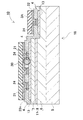
本発明の実施例1に係る発光装置1を図1の断面図に示す。この図の発光装置1に搭載される発光素子10は、窒化物半導体素子の一例であるLEDチップを採用しており、このLEDチップを配線基板9の一であるサブマウント上にフリップチップ実装している。フリップチップ実装とは、電極形成面と対向する成長基板5側を主光取出し面とする実装方式であり、フェイスダウン実装とも呼ばれる。図1の発光素子10は、フリップチップ実装であることを示すため、上下逆に表示している。
A light-emitting
図2は、図1の発光素子10であって、フリップチップ実装する前の状態、すなわち成長基板5を最下層にして、その上方に半導体構造11を積層した状態を示す概略断面図である。実際の発光装置の製造工程では、成長基板5の上面に各層が積層された窒化物半導体素子を上下逆にして図1のように実装する。以下、図2を用いて発光素子10の概略を説明する。また、図1の発光素子10において、図2に示す発光素子10と同様の構成には同一の符号を付して適宜説明を省略する。
FIG. 2 is a schematic cross-sectional view showing the state of the
図2に示す半導体発光素子10は、成長基板5と、その上面に成長された半導体構造11と、半導体構造11に電気的に接続された電極で構成される。半導体構造11は、第一半導体層と、活性領域8と、第二半導体層とを備える。例えば第一半導体層をn型半導体層6とする場合、第二半導体層はp型半導体層7となる。また活性領域8は、発光層に相当する。活性領域8が発する光の中心波長は、例えば360nm〜650nmとする。
A semiconductor
発光素子10は、活性領域8を有する半導体構造11を備える。図2の発光素子10では、対向する一対の主面を有する成長基板5の一方の主面上に、半導体構造11としての窒化物半導体層を積層して形成されている。具体的に、発光素子10は、成長基板5の上面側に、第一半導体層であるn型半導体層6、活性領域8、第二半導体層であるp型半導体層7とを順に備える窒化物半導体構造11が積層されている。また、n型半導体層6及びp型半導体層7には、電気的に接続される第一電極としてn側パッド電極3A及び第二電極としてp側パッド電極3Bを各々備える。発光素子10は、n側パッド電極3A及びp側パッド電極3Bを介して、外部より電力が供給されると、活性領域8から光を放出し、図2における成長基板5の下面側から、主に光が取り出される。すなわち図2の発光素子10では、成長基板5において、電極3A、3Bの装着面側(図2の上側)と対向する他方の主面側(図2の下側)を主な光取り出し面18とする。
(誘電体膜4)
The
(Dielectric film 4)
さらに、n側パッド電極3A、p側パッド電極3Bからなる一組の電極3は、誘電体膜4をそれぞれ有する。図3に、図2の太字の円に示す誘電体膜4の近傍における拡大断面図を示す。図3に示すように、誘電体膜4は、屈折率の異なる2種以上の材料膜4n、4mからなる1組の誘電体4aを、複数組にわたって積層させた多層構造である。誘電体膜4の詳細な構造については後述するが、誘電体膜4は、半導体構造11と電極3との間の少なくとも一部に設けられており、所定の波長光を選択的に反射できる。誘電体膜4は、互いに離間して形成することもできる。また、誘電体膜4は、SiO2、Al2O3等の単層膜としてもよい。単層膜の場合は光が反射せずに透過するため、特に非フリップチップ型の実装方法であるフェイスアップ型の半導体素子では、誘電体膜4の形成面における光取り出し効率が向上する。
(発光素子10)
Further, each of the pair of
(Light emitting element 10)
発光素子10として、例えば図2に示すLEDのような窒化物半導体素子では、成長基板5であるサファイア基板の上に、第一窒化物半導体層であるn型半導体層6、活性領域8である発光層、第二窒化物半導体層であるp型半導体層7を順にエピタキシャル成長させた窒化物半導体構造11と、さらに窒化物半導体構造11の上に形成された透光性導電層13とを有する。また誘電体層4と透光性導電層13との間には、反射層16が設けられる。この反射層16も、SiO2、Al2O3等の誘電体膜で構成され、全反射作用を発揮する。このように誘電体膜4に反射層16を組み合わせた反射構造とすることで、斜め成分の光に対しても高反射率を維持でき、高い取り出し効率が実現できる。
In the nitride semiconductor device such as the LED shown in FIG. 2 as the
続いて、活性領域8およびp型半導体層7の一部を選択的にエッチング除去して、n型半導体層6の一部を露出させ、さらにn側パッド電極3Aを形成している。またn側パッド電極3Aと同一面側であって、透光性導電層13上には、p側パッド電極3Bが形成される。さらに、n側パッド電極3A及びp側パッド電極3Bの所定の表面のみを露出し、他の部分は絶縁性の保護膜14で被覆される。なお、n側パッド電極3Aは、n型半導体層6の露出領域に、透光性導電層13を介して形成してもよい。以下に半導体発光素子10の各構成要素に関して、具体的に説明する。
(成長基板5)
Subsequently, the
(Growth substrate 5)
成長基板5は、半導体構造11をエピタキシャル成長させることができる基板で、基板の大きさや厚さ等は特に限定されない。窒化物半導体における基板としては、C面、R面、及びA面のいずれかを主面とするサファイアやスピネル(MgAl2O4)のような絶縁性基板、また炭化珪素(6H、4H、3C)、シリコン、ZnS、ZnO、GaAs、ダイヤモンド、及び窒化物半導体と格子接合するニオブ酸リチウム、ガリウム酸ネオジウム等の酸化物基板、GaNやAlN等の窒化物半導体基板があり、そのオフアングルした基板(例えば、サファイアC面で0.01°〜3.0°)も用いることができる。また、成長基板を半導体構造形成後に除去した基板の無い半導体素子構造、その取り出した半導体構造を支持基板、例えば導電性基板に接着、フリップチップ実装した構造等とすること、また別の透光性部材・透光性基板を半導体構造に接着した構造とするもできる。具体的には、半導体構造の光取り出し側の主面に成長基板、接着した部材・基板を有する場合は透光性とし、不透光性、遮光性、光吸収性の成長基板の場合は除去し、そのような基板に半導体構造を接着する場合は、半導体構造主面の光反射側に設ける構造とする。光取り出し側の透光性基板・部材から半導体構造に電荷を供給する場合は、導電性のものを用いると良い。その他、ガラス、樹脂などの透光性部材により半導体構造が接着・被覆されて、支持された構造の素子でも良い。成長用基板の除去は、例えば装置又はサブマウントのチップ載置部に保持して、研磨、LLO(Laser Lift Off)で実施できる。また、透光性の異種基板であっても、基板除去することで、光取り出し効率、出力を向上させることができ、好ましい。
(半導体構造11)
The
(Semiconductor structure 11)
半導体構造11としては、実施例及び以下で説明する窒化物半導体が、可視光域の短波長域、近紫外域、若しくはそれより短波長域である点、その点と光変換部材(蛍光体等)とを組み合わせた発光装置において好適に用いられる。あるいはこれらに限定されずに、InGaAs系、GaP系などの半導体でも良い。
(発光素子構造)
As the
(Light emitting element structure)
半導体構造11による発光素子構造は、後述する第一導電型(n型)、第二導電型(p型)層との間に活性領域8を有する構造が、出力、効率上好ましいが、それに限定されず後述する構造など、その他の発光構造でも良い。各導電型層に、絶縁、半絶縁性、逆導電型構造が一部に設けられても良く、またそれらが第一、二導電型層に対し付加的に設けられた構造でも良く、別の回路構造、例えば保護素子構造、を付加的に有しても良く、また、上記基板が発光素子の導電型の一部を担う構造でも良い。
The light emitting device structure using the
半導体構造11に設けられる電極は、実施例及び以下で説明する一方の主面側に第一導電型(n型)、第二導電型(p型)層の電極が設けられる構造が好ましいが、それに限定されず半導体構造の各主面に対向して各々電極が設けられる構造、例えば上記基板除去構造において除去側に電極を設ける構造としても良い。
The electrode provided in the
また、半導体構造11の構造としては、MIS接合、PIN接合やPN接合を有したホモ接合構造、ヘテロ接合構造あるいはダブルへテロ接合構造のものが挙げられる。また、各層を超格子構造としたり、発光層である活性領域8を量子効果が生ずる薄膜に形成させた量子井戸構造とすることもできる。
(窒化物半導体構造)
As the structure of the
(Nitride semiconductor structure)
窒化物半導体としては、一般式がInxAlyGa1-x-yN(0≦x、0≦y、x+y≦1)であって、BやP、Asを混晶してもよい。また、n型半導体層6、p型半導体層7は、単層、多層を特に限定しない。窒化物半導体構造11には発光層である活性領域8を有し、この活性領域8は単一(SQW)又は多重量子井戸構造(MQW)とする。以下に窒化物半導体構造11の詳細を示す。
As the nitride semiconductor, the general formula In x Al y Ga 1-xy N (0 ≦ x, 0 ≦ y, x + y ≦ 1) A, B and P, may be mixed with As. Further, the n-
成長基板5上に、バッファ層などの窒化物半導体の下地層、例えば低温成長薄膜GaNとGaN層、を介して、n型窒化物半導体層、例えばSiドープGaNのn型コンタクト層とGaN/InGaNのn型多層膜層、p型窒化物半導体層、例えばMgドープのInGaN/AlGaNのp型多層膜層とMgドープGaNのp型コンタクト層を有し、さらにそのp型、n型層の間に活性領域8を有する構造を用いる。
An n-type nitride semiconductor layer such as a Si-doped GaN n-type contact layer and a GaN / InGaN layer are formed on a
また、窒化物半導体の活性領域(発光層)8は、例えば、AlaInbGa1-a-bN(0≦a≦1、0≦b≦1、a+b≦1)からなる井戸層と、AlcIndGa1-c-dN(0≦c≦1、0≦d≦1、c+d≦1)からなる障壁層とを含む量子井戸構造を有する。活性領域8に用いられる窒化物半導体は、ノンドープ、n型不純物ドープ、p型不純物ドープのいずれでもよいが、好ましくは、ノンドープもしくは、又はn型不純物ドープの窒化物半導体を用いることにより発光素子を高出力化することができる。障壁層は井戸層よりもバンドギャップエネルギーの大きな窒化物半導体が用いられる。井戸層にAlを含ませることで、GaNのバンドギャップエネルギーである波長365nmより短い波長を得ることができる。活性領域8から放出する光の波長は、発光素子の目的、用途等に応じて360nm〜650nm付近、好ましくは380nm〜560nmの波長とする。
The active region (light emitting layer) 8 of the nitride semiconductor includes, for example, a well layer made of Al a In b Ga 1-ab N (0 ≦ a ≦ 1, 0 ≦ b ≦ 1, a + b ≦ 1), Al having c In d Ga 1-cd N (0 ≦ c ≦ 1,0 ≦ d ≦ 1, c + d ≦ 1) quantum well structure including a made of the barrier layer. The nitride semiconductor used for the
井戸層の組成はInGaNが、可視光・近紫外域に好適に用いられ、その時の障壁層の組成は、GaN、InGaNが良い。井戸層の膜厚は、好ましくは1nm以上30nm以下、より好ましくは2nm以上20nm以下である。 The composition of the well layer is preferably InGaN, and the composition of the barrier layer at that time is preferably GaN or InGaN. The thickness of the well layer is preferably 1 nm or more and 30 nm or less, more preferably 2 nm or more and 20 nm or less.
次に、p型半導体層7の表面に所定の形状をなすマスクを形成し、p型半導体層7及び発光層である活性領域8をエッチングする。これにより、所定の位置のn型半導体層6を構成するn型コンタクト層が露出される。
(透光性導電層13)
Next, a mask having a predetermined shape is formed on the surface of the p-
(Translucent conductive layer 13)
透光性導電層13は、n型半導体層6、p型半導体層7上にそれぞれ形成される。図2の例では、p型半導体層7及び露出したn型半導体層6のほぼ全面に透光性導電層13が形成されることにより、電流をp型半導体層7全体に均一に広げることができる。また、導電層が透光性を備えることで、さらにこの上に誘電体膜4を設けることができる。なお本明細書においてほぼ「全面に形成」とは、半導体構造の上方に形成されていることを言う。
The translucent
透光性導電層13は、透明電極など数々の種類があるが、好ましくはZn、In、Snよりなる群から選択された少なくとも一種の元素を含む酸化物とする。具体的には、ITO、ZnO、In2O3、SnO2等、Zn、In、Snの酸化物を含む透光性導電層13を形成することが望ましく、好ましくはITOを使用する。これにより当接する部材と良好なオーミック接触を得られる。あるいはNi、Au、Pt等の金属からなる3nm程度の薄膜の金属膜、その他の金属の酸化物、窒化物、それらの化合物、光透過構造やこれらの複合物でもよい。このように透光性導電層13は、各導電型層、例えばp型半導体層7のほぼ全面に形成され、電流を全体に均一に広げることができる。
The translucent
また、透光性導電層13の厚さは、その層の光吸収性と電気抵抗・シート抵抗、すなわち、光の誘電体膜4と電流広がりを考慮した厚さとし、例えば1μm以下、具体的には10nmから500nmとする。また、活性領域8から放出される光の波長λに対してλ/4のおよそ整数倍とすることが光取り出し効率が上がるので好ましい。
The thickness of the translucent
ここでは透光性導電層13であるITOの膜厚を700Åとする。また誘電体膜4は、図3の拡大断面図に示すように、ITO膜の上に反射層16として、厚膜のSiO2、Al2O3、Nb2O5等を形成した上で、Nb2O 5 /SiO2/Nb2O 5 /SiO2/Nb2O 5 /SiO2のように(Nb2O 5 /SiO2)を3ペアで構成し、膜厚を発光波長に合わせて調整するのが好ましい。バリア層24としてはRhを100Å成膜する。金属反射層22とパッド電極3は積層構造で、Al−Cu合金/Ti/Pt/Auの構造となる。バリア層24にAgを用いると吸収が低減され、更に取り出し効率が向上する。
(誘電体膜4)
Here, the film thickness of ITO which is the translucent
(Dielectric film 4)
誘電体膜4は、反射層16上に屈折率の異なる2種類の誘電体層を2〜5ペア、好ましくは3〜4ペア積層して構成する。また誘電体膜4の総膜厚は0.2〜1μmが好ましく、0.3〜0.6μmがより好ましい。これにより、誘電体膜4の干渉作用による光透過率の急峻な谷の発生を抑制でき、連続した高反射率な波長域を増大させることができる。この結果、誘電体膜4の中心波長を光源の発光ピーク波長よりも長波長側にずらしても、垂直入射の反射率の減少を抑止できる。つまり、入射角を持って誘電体膜4へと入射した光源の入射成分のみならず入射角の小さい入射成分をも反射可能となり、相対的に発光素子の光出力が向上する。好適には、誘電体膜4はSiO2とNb2O5のペアで構成する。この誘電体膜4は、波長及び方向依存による反射機能を発揮する。また誘電体膜4は、半導体発光素子10の電極形成側の面のほぼ全面に形成することが好ましい。
The
また誘電体膜4で、半導体構造11の側面、さらにはn電極とp電極の間を被覆することが好ましい。これにより、PNギャップ間での光のリークを抑制できる。
(開口部21)
Moreover, it is preferable that the
(Opening 21)
また、誘電体膜4には、開口部21を設ける。開口部21は、図2の断面図に示すように、透光性導電層13を部分的に表出させる。この結果、透光性導電層13は、開口部21を介して金属反射層22及びパッド電極3と電気的に接合される。
(バリア層24)
The
(Barrier layer 24)
バリア層24は、誘電体膜4が設けられていない開口部21に設けられて、開口部21で表出する透光性導電層13を被覆する。さらにこの上面を金属反射層22で被覆する。これによって、バリア層24が透光性導電層13と金属反射層22との間に介在されて、金属反射層22が直接透光性導電層13と接触する事態を回避でき、導通によって金属反射層22が透光性導電層13との接触面で劣化することを防止できる。このようなバリア層24には、Au、Ag、Pt、Pd、Rh、Ir、Ru、Osの群からなる少なくとも一の金属またはその合金からなる。好ましくは、Rhが好適に利用できる。またバリア層24の膜厚は、好ましくは誘電体膜4よりも薄く形成する。
The
バリア層24はスパッタリングや無電界めっき、蒸着等によって形成できる。スパッタリングでは、U字状に湾曲する。一方、無電界めっきでは、フラットに形成できる。
The
また、バリア層24と透光性導電層13の間にTi、Ni、Cr、Moの群からなる少なくとも一の金属またはその合金からなる密着層を有してもよい。この密着層によって、バリア層24と透光性導電層13との密着性が向上する。密着層は0.3〜50nm、好ましくは0.3〜3nmである。密着層の膜厚が薄い場合、活性領域8からの光は密着層を通過してバリア層24で反射されるため、バリア層24の高反射率の特性を利用でき、出力が高い。このとき、特に、バリア層はRhが好適に利用できる。
(金属反射層22)
Moreover, you may have the contact | adherence layer which consists of at least 1 metal which consists of a group of Ti, Ni, Cr, and Mo, or its alloy between the
(Metal reflective layer 22)
一方、金属反射層22は、バリア層24及び透光性導電層13を介して、半導体構造11を構成するn型層、p型層と電気的に接続される。このように金属反射層22は、導電層としての機能に加え、出力光を反射させる機能も奏することができる。この構造によって、半導体発光素子10は取り出し効率を高め、かつ信頼性を向上させることができる。金属反射層22は、Al、Cu、Au、Pt、Pd、Rh、Ni、W、Mo、Cr、Tiよりなる群から選択される。好適には、アルミニウム又はその合金とする。
On the other hand, the
金属反射層22とパッド電極3とは個別に形成してもよい。金属反射層22はAl若しくはその合金を用いる。また金属反射層22は発光領域のほぼ全面に形成する。パッド電極3は金属反射層22と異なるパターンで形成する場合は、フリップチップ実装時に使用する基板配線に合わせた設計が可能となる。この場合、パッド電極3の形成されていない領域には、絶縁性確保の為にSiO2からなる保護膜14を設ける。
The metal
一方でバリア層24が、各開口部21内にそれぞれ形成されている。このバリア層24は、開口部21内にのみ形成されており、またバリア層24と開口部21との個数は同じである。図2の例では、誘電体膜4とバリア層24のパターニングを同一のマスクで行い、パッド電極3と金属反射層22を同一のパターンで形成する。この結果、誘電体膜4の開口部21に正確にバリア層24を形成することができ、マスクを共通化してコストを削減すると共に、マスクの位置合わせ作業も一度で済む。特にバリア層24のパターンを誘電体膜4と同じマスクで行うことで、位置ずれが発生せず、歩留まりが向上して高品質な製品とできる。また作業を連続的に行えることから、製造工程も簡素化できる。また、位置ずれに対してのマージンをバリア設計に考慮しなくても良いので、金属反射層の有効面積を上げることができ、取り出し効率が向上する。
On the other hand, a
このように、誘電体膜4に形成した開口部21の内部に開口径に合わせたバリア層24を形成することで、透光性導電層13と金属反射層22との直接の接触を回避しつつ、金属反射層22として反射率の高い金属を利用できる。また誘電体膜4と金属反射層22とを分離することにより、誘電体膜4を半導体発光素子10の全面に形成することを可能としている。この結果、PNギャップ間の光の漏れを低減することが可能となる。またバリア層24として、更に高反射のAg系の材料を用いることで、取り出し効率の一層の向上が可能となる。このバリア層24は素子構造の内部に形成されるため、イオンマイグレーションも回避できる。
Thus, by forming the
以上説明した半導体発光素子10は、フリップチップ(フェイスダウン)で使用される。ただ、本発明はフリップチップ構造に限られず、フェイスアップ構成で用いることも可能である。
(実施例2)
The semiconductor
(Example 2)
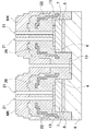
さらに、パッド電極の上に共晶パッド電極を設けることもできる。この例を実施例2として図4〜図7に示す。これらの図において、図4は模式断面図を示している。また図5〜図7は、実際の層構成の一例であって、図5は平面図、図6Aは図5のVI−VI線における断面図、図7は図5のVII−VII線における断面図を、それぞれ示している。これらの図に示す半導体発光素子10’は、図2とほぼ同様の構成を備えており、同一の部材には同一の符号を付して詳細説明を省略する。図4において半導体発光素子10’の表面には、パッド電極の形成された部分を除いて、絶縁性の保護膜14で被覆される。また開口部21に形成されるバリア層24は、図4の例では開口部21の底面のみに平板状に形成されているが、図6Aに示すように、開口部21の底面から周壁にかけて凹状に形成することもできる。これにより、バリア層24と接する誘電体膜4の側面においても光を反射させることができる。さらに図6Aにおいて、パッド電極3の上面に共晶パッド電極27を設けている。
また開口部にバリア層を設けることで、その上に積層する金属反射層の断線を防止できるという利点も得られる。この様子を、図6Bに基づいて説明する。図6Bは、開口部21にバリア層24を設けた上で直接金属反射層22を成長させた例の模式断面図を示している。バリア層のない状態で開口部21に直接、金属反射層22を成長させると、金属反射層22は垂直方向には成長するが横方向には成長し難く、特に誘電体膜4の側面と上面の境界であるエッジの部分で金属反射層22が部分的に薄くなることがある。この結果、金属反射層22の薄い部分では電気抵抗値が部分的に高くなり、電流が流れ難くなる。また、この部分で金属反射層22にバリが発生する等して物理的な接触不良や断線の可能性もあった。特に、誘電体膜4の側面が垂直に近くなる程、この状態が顕著となる。そこで、誘電体膜4の側面を図6Aに示すように傾斜させることで、誘電体膜4のエッジ部分を鈍角にして開口部21の段差を緩やかにする。これにより、金属反射層22がこのエッジ部分で急峻に成長方向を変えられて薄くなる事態が低減されて、綺麗に金属反射層22を成膜できる。また、開口部21の底面にバリア層24を設け、開口部21の深さを浅くすることでも、エッジ部分で金属反射層22が部分的に薄くなることを軽減できる。
また、誘電体膜4の側面を傾斜させてエッジ部分を鈍角にすることに加えて、誘電体膜4の側面にバリア層24を設けることで、この角度をさらに大きくでき、鈍角を大きくすることで開口部21の段差を一層緩やかにして金属反射層22の信頼性を高める効果を一層改善できる。ただ本発明は、誘電体膜の側面を傾斜面に特定するものでなく、垂直面あるいは垂直面に近い角度として、誘電体膜側面のバリア層でもって開口部の段差を緩やかにする構成も採用できる。
さらに図6Aのように、開口部21の底面のみならず、周壁にバリア層24を設けることでも、同様に誘電体膜4のエッジ部分で金属反射層22が薄くなる事態を低減できる。すなわち図6Bに示すように、バリア層24を誘電体膜4のエッジ部分から開口部21の底面に向かって勾配させるように設けることでも、エッジ部分を鈍角にできるので、同様に金属反射層22が部分的に薄くなる事態を回避して綺麗に成膜できる。
具体的には、図6Bに示すように、誘電体膜4の側面に設けられたバリア層24の傾斜面の角度αを、誘電体膜4の側面の傾斜角度βよりも大きくすることが好ましい。また、誘電体膜4の側面に設けられたバリア層24の厚さが、開口部21において上部で狭く(厚さc)、下部で広くなるように(厚さd)することが好ましい。下部の厚さdは、例えばバリア層24の傾斜面を開口部21の底面側に向かって延長させた場合の、交点と誘電体膜4との距離で規定できる。
Furthermore, a eutectic pad electrode can be provided on the pad electrode. This example is shown as a second embodiment in FIGS. In these drawings, FIG. 4 shows a schematic cross-sectional view. 5 to 7 are examples of actual layer configurations, FIG. 5 is a plan view, FIG. 6A is a cross-sectional view taken along the line VI-VI in FIG. 5, and FIG. 7 is a cross-sectional view taken along the line VII-VII in FIG. Each figure is shown. The semiconductor
In addition, by providing a barrier layer in the opening, there is also an advantage that disconnection of the metal reflective layer laminated thereon can be prevented. This will be described with reference to FIG. 6B. FIG. 6B shows a schematic cross-sectional view of an example in which the
Further, in addition to inclining the side surface of the
Further, as shown in FIG. 6A, the provision of the
Specifically, as shown in FIG. 6B, the angle α of the inclined surface of the
ここで比較例として、図5の半導体発光素子の特性を図31の構造を用いた発光素子と比較した。これらの光出力と順方向電圧を比較した結果を、図8のグラフに示す。このグラフに示すように、光出力は向上が見られる一方で、順方向電圧が低下していることが確認され、実施例2に係る構造の有用性が裏付けられた。
(実施例3)
Here, as a comparative example, the characteristics of the semiconductor light emitting device of FIG. 5 were compared with those of the light emitting device using the structure of FIG. FIG. 8 is a graph showing the result of comparing the light output and the forward voltage. As shown in this graph, it was confirmed that the light output was improved while the forward voltage was reduced, and the usefulness of the structure according to Example 2 was confirmed.
Example 3
さらに半導体発光素子は、外部接続のためのパッド電極同士の間にギャップを設けることもできる。このような半導体発光素子10”を実施例3として図9に示す。ここで実施例3に係る半導体発光素子の製造方法について、図10のフローチャートと図11A〜E、図12F〜Iの断面図に基づいて説明する。なおこれらの図においては、説明のためダイス単体を示しており、ウェハプロセス後のチップ化工程については省略している。大まかな手順としては、
ステップS1:エピ受け入れ
ステップS2:n型層出し
ステップS3:ITOオーミック電極形成
ステップS4:全面DBR成膜
ステップS5:開口部形成用レジストマスク形成
ステップS6:DBR膜ドライエッチ
ステップS7:バリアメタル成膜
ステップS8:リフトオフ
ステップS9:パッド電極形成
となる。
Further, in the semiconductor light emitting device, a gap can be provided between pad electrodes for external connection. 9 such a semiconductor
Step S1: Epi acceptance step S2: N-type layer deposition step S3: ITO ohmic electrode formation step S4: Full-surface DBR film formation step S5: Opening formation resist mask formation step S6: DBR film dry etching step S7: Barrier metal film formation Step S8: Lift-off step S9: Pad electrode formation.
まず図11Aに示すようにGaN層を成長させると共に、図11Bに示すようにGaN層上にSiO2やレジスト等のマスクを形成し、RIE等によりnコンタクト用にn型半導体層6を露出させる。そしてRIEマスクを除去後、図11Cに示すように透光性導電層13としてITO電極を成膜して、パターニングを行う。ITO電極の成膜方法としては、蒸着やスパッタ等が上げられる。またパターニングに関しては、エッチング若しくはリフトオフが適宜選択可能である。次に、図11Dに示すように誘電体膜4を全面(半導体構造11の上方と側面の両方を含む。)に成膜する。膜形成方法としては、スパッタ及び蒸着等が利用できる。そして誘電体膜4の成膜後に、図11Eに示すように導通部に合わせて開口部21を設けたマスクMKをフォトレジストにより形成する。そして、図12Fに示すように誘電体膜4のエッチングを行う。このエッチングはウェットエッチングやRIEによるドライエッチングが選択できる。またエッチング時に誘電体膜4にテーパを形成すれば、後の工程でリフトオフ作業を容易とできる。ドライエッチングの終了後、図12Gに示すようにマスクMKを除去せず、そのマスクMKをそのまま使用してバリア層24をリフトオフ形成する。バリア層24として用いる金属は、ITO電極との反応を避けるため、Au、Rh、Pt、Pd、Au、Ag等の仕事関数の高い金属が望ましい。このようにして、開口部21にバリア層24を形成した後、図12Hに示すようにマスクMKを除去し、さらに図12Iに示すようにAl若しくはその合金からなる金属反射層22と、接続用のパッド電極3A、3Bを形成する。
First with a GaN layer is grown as shown in FIG. 11 A, a mask such as SiO 2 or resist is formed on the GaN layer as shown in FIG. 11 B, the n-
このような手順によって、バリア層24の形成のためのマスクMKを、誘電体膜4に開口部21を形成するためのマスクMKと共通化でき、製造工数を低減できる。加えて、バリア層24形成時に開口部21に位置決めする作業が不要となり、高精度なバリア層24の成形が実現できる。
(実施例4)
By such a procedure, the mask MK for forming the
Example 4
さらに、実施例4に係る半導体発光素子(図21の断面図)の製造手順を、図13〜図21の断面図に示す。まず図13においては、半導体構造11をエピタキシャル成長させた後、n型半導体層6を構成するGaN層をエッチングして、露出させる。その上で、透光性導電層13としてITOを成膜する。次に図14において誘電体膜4(DBR)を形成し、さらに金属反射層22としてAl層を形成する。さらに図15でフォトリソグラフィなどによってマスクMKとしてレジスト層を形成して表面を被覆し、金属反射層22をエッチングする。次いで図16でレジスト層を除去し、さらに図17で絶縁膜を成膜する。さらに図18に示すように、フォトリソグラフィなどによってレジスト層を形成し、絶縁膜と誘電体膜4のエッチングを行う。次いで図19においてバリア層24を成膜し、図20でリフトオフを行いレジスト層を剥離させる。最後に図21でフォトリソグラフを行い、バリア層24の上面にパッド電極としてAl層を成膜し、リフトオフによってレジスト層を除去する。このようにして、実施例4に係る半導体発光素子が製造される。
(実施例5)
Furthermore, the manufacturing procedure of the semiconductor light emitting device (cross-sectional view of FIG. 21) according to Example 4 is shown in the cross-sectional views of FIGS. First, in FIG. 13, after the
(Example 5)
さらに、Al反射膜をより広い面積で設けることもできる。このような例を実施例5として図22の断面図に示す。図22の構造ではAl反射膜を多層配線にしてAl反射膜の隙間をなくしているため、光の漏れを抑制することができ、光出力の向上の面では有利となる。
(実施例6)
(共晶実装)
Furthermore, the Al reflective film can be provided in a wider area. Such an example is shown as a fifth embodiment in the sectional view of FIG. In the structure of FIG. 22, since the Al reflective film is formed as a multilayer wiring and the gap between the Al reflective films is eliminated, light leakage can be suppressed, which is advantageous in improving the light output.
(Example 6)
(Eutectic mounting)
また半導体発光素子は、共晶実装に対応させることもできる。このような例を実施例6として図23の断面図に示す。これらの図に示す発光素子は、まず成長基板5上にn型層を積層後、n型層の一部をエッチングして露出させ、透光性導電層13としてITO層を積層する。さらにDBRとバリア層24を積層し、金属反射層22を形成後、電極絶縁膜26を設けて、最後に共晶パッド電極を積層する。
(n側電極3a)
In addition, the semiconductor light emitting element can be adapted to eutectic mounting. Such an example is shown as a sixth embodiment in the sectional view of FIG. In the light emitting device shown in these figures, an n-type layer is first laminated on the
(N-
またn側電極3aは、小径化して分散して配置することが好ましい。n側電極3aは、さらにn側パッド電極3Aと接続することにより、電極の面積を大きくすることができ、放熱性と実装性とが良好な素子となる。このような例を図24の水平断面図に示す。この図に示すようにn側電極3aを小径化させることによって、出力光がn側電極3aで吸収されることを低減して、結果的に光の取り出し効率を向上させることができる。加えて、小径化させたn側電極3aを分散して配置することで、抵抗値を低減してVfを低減でき、出力のリニアリティが向上し、また出力光を吸収するn側電極3aを分散配置することで発光分布を均一化する効果も得られる。ここで、「分散して配置する」とは、複数のn側電極3aが集まって一群となったものが分散配置されていてもよいし、個々のn側電極3aが集合体を作らずに分散配置されていてもよい。
(実施例7)
(立体配線)
(電極絶縁膜26)
Further, the n-
(Example 7)
(Three-dimensional wiring)
(Electrode insulating film 26)
また半導体発光素子は、立体配線に対応させることもできる。このような例を実施例7として図25、図26に示す。これらの図において、図25は発光素子の平面図、図26は図25のXXVI−XXVI線における垂直断面図を、それぞれ示している。立体配線においては、p側電極3b、n側電極3aを一旦電極絶縁膜26で被覆した後、この電極被覆膜に開口された導通窓を通じて、p側パッド電極3B、n側パッド電極3Aを設ける。このようにすることで、パッド電極を広くしても、その下面が電極絶縁膜26で絶縁されているため短絡することがなく、結果的に電極面積を広く確保でき、共晶などによって固定、導通に十分な面積を容易に確保できる利点が得られる。例えば、図26の断面図に示す例では、n側電極3aを、電極絶縁膜26を介して広いnパッド電極に拡大させることができ、共晶のための面積を広く確保でき、共晶の信頼性を高めて安定した実装が実現される。共晶以外の実装、例えばAuスタッドバンプを用いた超音波接合でもバンプ数を増やすことができ、放熱性が改善する。この結果、高電流を通電することが可能となる。また、PNギャップ間では電流が集中して熱を帯びやすいため、複数のn側電極3aに囲まれるように、n側パッド電極3A上にスタッドバンプを形成すれば、放熱性がさらに良好となる。
In addition, the semiconductor light emitting element can be adapted to three-dimensional wiring. Such an example is shown as
これらの図に示す発光素子は、まず成長基板5上にn型層を積層後、n型層の一部をエッチングして露出させ、ITO層を積層する。以下、図23と同様にDBRとバリア層24を積層し、金属反射層22を形成後、電極絶縁膜26を設けて、最後に共晶パッド電極を積層する。このように、n電極とp電極とがオーバーラップするように、立体配線構造を採用することで、本来であればn側電極3aのようにn電極が小さいところ、図25のn側パッド電極3Aように広い面積に拡大できるので、電極面積を広く取ることで共晶実装に有利となる。
In the light emitting device shown in these drawings, an n-type layer is first laminated on the
さらに誘電体膜4を層間絶縁膜として利用した立体配線構造とすることで、発光に寄与しないn型コンタクト層の面積をできるだけ小さくすると共に、フリップチップ接合に必要な接合面積の確保が可能となる。
(実施例8)
Furthermore, by adopting a three-dimensional wiring structure using the
(Example 8)
更に他の実施例として実施例8に係る半導体発光素子を、図27〜図28に示す。これらの図において、図27は発光素子の平面図、図28は図27のXXVIII−XXIII線における断面図である。このように、平面図が正方形状でなく長方形状の発光素子においても、立体配線によって電極面積を広く取ることが可能となり、共晶実装に有利とできる。
(電極絶縁膜26)
As still another example, a semiconductor light emitting device according to Example 8 is shown in FIGS. In these drawings, FIG. 27 is a plan view of the light-emitting element, and FIG. 28 is a cross-sectional view taken along line XXVIII-XXIII in FIG. As described above, even in a light-emitting element having a rectangular shape in plan view, the electrode area can be widened by three-dimensional wiring, which is advantageous for eutectic mounting.
(Electrode insulating film 26)
半導体構造11の側面は、金属反射層22で被覆される。半導体構造11の側面を被覆する金属反射層22は、n型半導体層6を被覆している。またp型半導体層7を被覆する第二金属反射層22nとは分離されており、金属反射層22と第二金属反射層22nとは離間されている。さらに、半導体構造11の側面を被覆する金属反射層22の上面には、電極絶縁膜26を設けている。電極絶縁膜26は、金属反射層22及び第二金属反射層22nの離間された領域を覆うように延長されている。この電極絶縁膜26の上面に、n側パッド電極及びp側パッド電極を離間させている。これにより、n側電極3aとp側電極3bとを立体配線構造として、より広い面積でパッド電極を設けることができ、共晶に有利となる。このように誘電体膜4を層間絶縁膜とした立体配線構造とすることで、電極で光を遮断する事態を避け、光取り出し効率を一層向上できる。
The side surface of the
本発明の半導体発光素子は、照明用光源、LEDディスプレイ、バックライト光源、信号機、照明式スイッチ、各種センサ及び各種インジケータ等に好適に利用できる。 The semiconductor light emitting device of the present invention can be suitably used for illumination light sources, LED displays, backlight light sources, traffic lights, illumination switches, various sensors, various indicators, and the like.
1…発光装置
3…電極;3a…n側電極;3b…p側電極
3A…n側パッド電極;3B…p側パッド電極;303、333…パッド電極
4、294、304、334…誘電体膜;4a…1組の誘電体;4n、4m…材料膜
5、305…成長基板
6…n型半導体層
7…p型半導体層
8…活性領域;298、308…発光層
9…配線基板;309…実装基板
10、10’、10”…半導体発光素子
11…半導体構造
13…透光性導電層;2913、3013、3313…ITO膜
14、3014…保護膜
16、2916…反射層
18、2918、3018…光取り出し面
2920、3020…反射構造
21、2921…開口部
22、3022、3322…金属反射層;22n…第二金属反射層
23、2923、3023…金属電極層
24…バリア層
26…電極絶縁膜
27…共晶パッド電極
3028…絶縁性誘電体膜
MK…マスク
DESCRIPTION OF
Claims (15)
前記半導体構造の上面に形成される透光性導電層と、
前記透光性導電層の上面に形成される誘電体膜と、
前記誘電体膜の上面に形成される金属反射層と、
を備える半導体発光素子であって、
前記誘電体膜は、前記透光性導電層を部分的に表出させるように、1以上の開口部を設けており、
前記透光性導電層は、前記開口部を介して前記金属反射層と電気的に接合されており、
前記開口部の底面及びその周壁である前記誘電体膜の側面を被覆するように、部分的にバリア層が形成され、該バリア層が前記透光性導電層と金属反射層との間に介在されており、
前記誘電体膜の側面に設けられた前記バリア層の厚さが、前記開口部において上部で狭く、下部で広くなるように構成してなることを特徴とする半導体発光素子。 A semiconductor structure including an active region;
A translucent conductive layer formed on an upper surface of the semiconductor structure;
A dielectric film formed on an upper surface of the translucent conductive layer;
A metal reflective layer formed on the top surface of the dielectric film;
A semiconductor light emitting device comprising:
The dielectric film has one or more openings so as to partially expose the translucent conductive layer,
The translucent conductive layer is electrically joined to the metal reflective layer through the opening,
A barrier layer is partially formed so as to cover the bottom surface of the opening and the side surface of the dielectric film that is the peripheral wall thereof, and the barrier layer is interposed between the translucent conductive layer and the metal reflective layer. Has been
A semiconductor light emitting device , wherein the thickness of the barrier layer provided on the side surface of the dielectric film is configured to be narrow at the top and wide at the bottom in the opening .
前記誘電体膜が多層からなることを特徴とする半導体発光素子。 The semiconductor light emitting device according to claim 1,
A semiconductor light-emitting element, wherein the dielectric film is composed of multiple layers.
前記金属反射層が、アルミニウム又はその合金からなることを特徴とする半導体発光素子。 The semiconductor light-emitting device according to claim 1 or 2,
The semiconductor light emitting element, wherein the metal reflective layer is made of aluminum or an alloy thereof.
前記バリア層が、Au、Ag、Pt、Pd、Rh、Ir、Ru、Osの群からなる少なくとも一の金属またはその合金からなることを特徴とする半導体発光素子。 The semiconductor light-emitting device according to claim 1,
The semiconductor light emitting element, wherein the barrier layer is made of at least one metal made of Au, Ag, Pt, Pd, Rh, Ir, Ru, Os or an alloy thereof.
さらに前記バリア層と透光性導電層の間にTi、Ni、Cr、Moの群からなる少なくとも一の金属またはその合金からなる密着層を有することを特徴とする半導体発光素子。 The semiconductor light-emitting device according to claim 1,
Furthermore, the semiconductor light emitting element characterized by having the contact | adherence layer which consists of at least 1 metal which consists of a group of Ti, Ni, Cr, Mo, or its alloy between the said barrier layer and a translucent conductive layer.
前記透光性導電層が、ITOで構成されてなることを特徴とする半導体発光素子。 A semiconductor light emitting device according to any one of claims 1 to 5,
The light-transmitting conductive layer is made of ITO, and is a semiconductor light emitting device.
前記バリア層は、その膜厚が前記誘電体膜よりも薄く形成されてなることを特徴とする半導体発光素子。 The semiconductor light-emitting device according to claim 1,
The barrier layer is formed so as to have a film thickness thinner than that of the dielectric film.
前記バリア層が、前記開口部内にのみ形成されてなることを特徴とする半導体発光素子。 The semiconductor light-emitting device according to claim 1,
The semiconductor light emitting element, wherein the barrier layer is formed only in the opening.
前記誘電体膜が、開口部を除いて前記半導体構造のほぼ全面に形成されてなることを特徴とする半導体発光素子。 The semiconductor light-emitting device according to claim 1,
A semiconductor light-emitting element, wherein the dielectric film is formed on substantially the entire surface of the semiconductor structure except for an opening .
前記透光性導電層が、前記半導体構造のほぼ全面に形成されてなることを特徴とする半導体発光素子。 A semiconductor light emitting device according to any one of claims 1 to 9,
A semiconductor light-emitting element, wherein the translucent conductive layer is formed on substantially the entire surface of the semiconductor structure.
前記誘電体膜で、前記半導体構造の側面を被覆してなることを特徴とする半導体発光素子。 The semiconductor light-emitting device according to claim 1,
A semiconductor light emitting device, wherein the dielectric film covers a side surface of the semiconductor structure.
前記金属反射層の上面に形成されるパッド電極を備え、
前記パッド電極を構成するn側電極が、複数に分割された小径化電極として、分散して配置されてなることを特徴とする半導体発光素子。 The semiconductor light-emitting device according to claim 1, further comprising:
A pad electrode formed on the upper surface of the metal reflective layer;
The n-side electrode which comprises the said pad electrode is disperse | distributed and arrange | positioned as a reduced diameter electrode divided | segmented into plurality, The semiconductor light-emitting device characterized by the above-mentioned.
前記金属反射層で、前記半導体構造の側面を被覆してなることを特徴とする半導体発光素子。 The semiconductor light emitting device according to claim 12,
A semiconductor light emitting device, wherein the metal reflective layer covers a side surface of the semiconductor structure.
前記半導体構造の側面を被覆する前記金属反射層は、前記半導体構造を構成するn型半導体層を被覆してなり、
かつ前記半導体構造を構成するp型半導体層を被覆する第二金属反射層と離間されてなることを特徴とする半導体発光素子。 The semiconductor light emitting device according to claim 13, further comprising:
The metal reflection layer covering the side surface of the semiconductor structure covers an n-type semiconductor layer constituting the semiconductor structure,
A semiconductor light emitting device, wherein the semiconductor light emitting device is separated from a second metal reflection layer covering the p-type semiconductor layer constituting the semiconductor structure.
前記半導体構造の側面を被覆する前記金属反射層の上面に、さらに電極絶縁膜を設けており、
前記電極絶縁膜は、前記金属反射層及び第二金属反射層の離間された領域を覆うように延長されてなり、
さらに該電極絶縁膜の上面に、前記パッド電極として、n側パッド電極及びp側パッド電極が離間されて設けられてなることを特徴とする半導体発光素子。 15. The semiconductor light emitting device according to claim 14, further comprising:
An electrode insulating film is further provided on the upper surface of the metal reflective layer covering the side surface of the semiconductor structure,
The electrode insulating film is extended so as to cover the separated regions of the metal reflective layer and the second metal reflective layer,
Further, an n-side pad electrode and a p-side pad electrode are provided on the upper surface of the electrode insulating film as the pad electrodes, and are separated from each other.
Priority Applications (1)
| Application Number | Priority Date | Filing Date | Title |
|---|---|---|---|
| JP2012173449A JP5949294B2 (en) | 2011-08-31 | 2012-08-03 | Semiconductor light emitting device |
Applications Claiming Priority (5)
| Application Number | Priority Date | Filing Date | Title |
|---|---|---|---|
| JP2011189889 | 2011-08-31 | ||
| JP2011189889 | 2011-08-31 | ||
| JP2012168944 | 2012-07-30 | ||
| JP2012168944 | 2012-07-30 | ||
| JP2012173449A JP5949294B2 (en) | 2011-08-31 | 2012-08-03 | Semiconductor light emitting device |
Publications (2)
| Publication Number | Publication Date |
|---|---|
| JP2014044971A JP2014044971A (en) | 2014-03-13 |
| JP5949294B2 true JP5949294B2 (en) | 2016-07-06 |
Family
ID=46762923
Family Applications (1)
| Application Number | Title | Priority Date | Filing Date |
|---|---|---|---|
| JP2012173449A Active JP5949294B2 (en) | 2011-08-31 | 2012-08-03 | Semiconductor light emitting device |
Country Status (6)
| Country | Link |
|---|---|
| US (1) | US8823031B2 (en) |
| EP (1) | EP2565944B1 (en) |
| JP (1) | JP5949294B2 (en) |
| KR (1) | KR101627010B1 (en) |
| CN (2) | CN102969414B (en) |
| TW (1) | TWI555231B (en) |
Families Citing this family (74)
| Publication number | Priority date | Publication date | Assignee | Title |
|---|---|---|---|---|
| US9142740B2 (en) | 2003-07-04 | 2015-09-22 | Epistar Corporation | Optoelectronic element and manufacturing method thereof |
| JP5768759B2 (en) * | 2012-04-27 | 2015-08-26 | 豊田合成株式会社 | Semiconductor light emitting device |
| KR102005235B1 (en) * | 2013-03-06 | 2019-07-30 | 삼성전자주식회사 | Light Emitting diode package having flip-chip bonding structure |
| KR20150025231A (en) * | 2013-08-28 | 2015-03-10 | 서울반도체 주식회사 | Light source module and manufacturing method thereof, backlight unit |
| JP6306308B2 (en) * | 2013-09-19 | 2018-04-04 | 株式会社東芝 | Semiconductor light emitting device |
| WO2015053595A1 (en) * | 2013-10-11 | 2015-04-16 | 주식회사 세미콘라이트 | Semiconductor light-emitting diode |
| JP6252123B2 (en) * | 2013-11-14 | 2017-12-27 | 日亜化学工業株式会社 | Method for manufacturing light emitting device |
| EP2942815B1 (en) * | 2014-05-08 | 2020-11-18 | Nexperia B.V. | Semiconductor device and manufacturing method |
| JP6720472B2 (en) * | 2014-06-13 | 2020-07-08 | 日亜化学工業株式会社 | Method of manufacturing light emitting device |
| CN104103733B (en) * | 2014-06-18 | 2018-06-05 | 华灿光电(苏州)有限公司 | A kind of upside-down mounting LED chip and its manufacturing method |
| CN105226140B (en) * | 2014-06-19 | 2018-06-01 | 映瑞光电科技(上海)有限公司 | Flip LED chips preparation method |
| CN104037277A (en) * | 2014-06-26 | 2014-09-10 | 圆融光电科技有限公司 | LED flip chip manufacturing method and LED flip chip |
| WO2016011606A1 (en) * | 2014-07-23 | 2016-01-28 | 深圳市国源铭光电科技有限公司 | Manufacturing method for led light source, and batch manufacturing method |
| US9923121B2 (en) * | 2014-08-05 | 2018-03-20 | Seoul Viosys Co., Ltd. | Light-emitting diode and manufacturing method therefor |
| CN104134723A (en) * | 2014-08-08 | 2014-11-05 | 映瑞光电科技(上海)有限公司 | Vertical type LED chip structure and manufacturing method thereof |
| JP6413460B2 (en) * | 2014-08-08 | 2018-10-31 | 日亜化学工業株式会社 | LIGHT EMITTING DEVICE AND LIGHT EMITTING DEVICE MANUFACTURING METHOD |
| US9433050B2 (en) * | 2014-10-08 | 2016-08-30 | Mikro Mesa Technology Co., Ltd. | Micro-light-emitting diode |
| CN104300056B (en) * | 2014-10-11 | 2017-07-07 | 广东晶科电子股份有限公司 | A kind of preparation method of the flip LED chips of high reliability, LED component and LED chip |
| KR102282137B1 (en) * | 2014-11-25 | 2021-07-28 | 삼성전자주식회사 | Semiconductor light emitting device and semiconductor light emitting apparatus having the same |
| CN105870280B (en) * | 2015-01-21 | 2019-07-09 | 展晶科技(深圳)有限公司 | LED crystal particle |
| JP2016146389A (en) * | 2015-02-06 | 2016-08-12 | 株式会社東芝 | Semiconductor light-emitting element and method of manufacturing the same |
| TWI710144B (en) * | 2015-02-17 | 2020-11-11 | 新世紀光電股份有限公司 | Light emitting diode with Bragg reflector and manufacturing method thereof |
| TWI583019B (en) * | 2015-02-17 | 2017-05-11 | 新世紀光電股份有限公司 | Light emitting diode and manufacturing method thereof |
| KR102038443B1 (en) | 2015-03-26 | 2019-10-30 | 엘지이노텍 주식회사 | Light emitting device and light emitting device package |
| US9960321B2 (en) | 2015-07-01 | 2018-05-01 | Sensor Electronic Technology, Inc. | Multi-layered contact to semiconductor structure |
| CN106486572B (en) | 2015-09-02 | 2020-04-28 | 新世纪光电股份有限公司 | Light emitting diode chip |
| JP2017054901A (en) * | 2015-09-09 | 2017-03-16 | 豊田合成株式会社 | Group iii nitride semiconductor light emitting device and manufacturing method of the same |
| KR101890691B1 (en) * | 2016-03-09 | 2018-09-28 | 유태경 | Semiconductor light emitting element |
| KR102443694B1 (en) * | 2016-03-11 | 2022-09-15 | 삼성전자주식회사 | Light emitting diode(LED) device for improving current spread characteristics and light extraction efficiency |
| JP2017183458A (en) | 2016-03-30 | 2017-10-05 | ソニー株式会社 | Light-emitting element assembly, its manufacturing method, and display device |
| DE102016106831A1 (en) * | 2016-04-13 | 2017-10-19 | Osram Opto Semiconductors Gmbh | Optoelectronic semiconductor chip |
| KR101803545B1 (en) | 2016-05-10 | 2018-01-11 | 재단법인대구경북과학기술원 | Reflecting electrode for light emitting diode and preparation method thereof |
| KR102519668B1 (en) | 2016-06-21 | 2023-04-07 | 삼성전자주식회사 | Semiconductor light-emitting device and method for manufacturing the same |
| KR102476139B1 (en) | 2016-08-03 | 2022-12-09 | 삼성전자주식회사 | Semiconductor light emitting device |
| CN111129264B (en) * | 2016-09-05 | 2023-11-17 | 首尔伟傲世有限公司 | Chip-scale package light-emitting diode |
| CN106252477B (en) * | 2016-10-31 | 2018-11-02 | 江苏新广联科技股份有限公司 | A kind of the flip LED chips structure and production method of compound total reflection mirror |
| KR102588170B1 (en) * | 2016-11-16 | 2023-10-13 | 삼성전자주식회사 | Semiconductor light emitting device having a reflector layer of multilayer structure |
| KR102555005B1 (en) * | 2016-11-24 | 2023-07-14 | 삼성전자주식회사 | Semiconductor light emitting device and method of manufacturing the same |
| CN114388674B (en) * | 2016-12-21 | 2024-07-12 | 首尔伟傲世有限公司 | High-reliability light-emitting diode |
| CN207676936U (en) * | 2017-01-06 | 2018-07-31 | 首尔伟傲世有限公司 | Light-emitting component with current barrier layer |
| US10396248B2 (en) | 2017-04-17 | 2019-08-27 | Lumens Co., Ltd. | Semiconductor light emitting diode |
| KR102302593B1 (en) | 2017-07-13 | 2021-09-15 | 삼성전자주식회사 | Light emitting device, package having the same, and method for manufacturing the same |
| KR102499308B1 (en) * | 2017-08-11 | 2023-02-14 | 서울바이오시스 주식회사 | Light emitting diode |
| KR102370621B1 (en) * | 2017-08-24 | 2022-03-04 | 삼성전자주식회사 | Light emitting package and light emitting module including the same |
| JP7308831B2 (en) * | 2017-12-14 | 2023-07-14 | ルミレッズ リミテッド ライアビリティ カンパニー | Method to prevent LED die contamination |
| US10522708B2 (en) | 2017-12-14 | 2019-12-31 | Lumileds Llc | Method of preventing contamination of LED die |
| US20190189850A1 (en) * | 2017-12-19 | 2019-06-20 | Epistar Corporation | Light-emitting device |
| CN115621388A (en) | 2017-12-22 | 2023-01-17 | 首尔伟傲世有限公司 | Light emitting diode |
| KR102601421B1 (en) * | 2018-12-06 | 2023-11-14 | 서울바이오시스 주식회사 | Chip scale packaged light emitting diode |
| KR102440223B1 (en) * | 2017-12-22 | 2022-09-06 | 서울바이오시스 주식회사 | Chip scale packaged light emitting diode |
| KR102427642B1 (en) | 2018-01-25 | 2022-08-01 | 삼성전자주식회사 | Semiconductor light emitting device |
| KR102543183B1 (en) | 2018-01-26 | 2023-06-14 | 삼성전자주식회사 | Semiconductor light emitting device |
| US11637223B2 (en) * | 2018-04-08 | 2023-04-25 | Xiamen Sanan Optoelectronics Technology Co., Ltd. | Light emitting diode device |
| KR102573271B1 (en) * | 2018-04-27 | 2023-08-31 | 삼성전자주식회사 | Semiconductor light emitting device |
| CN111200049A (en) * | 2018-05-02 | 2020-05-26 | 首尔伟傲世有限公司 | Light emitting element package |
| JP7219552B2 (en) | 2018-05-15 | 2023-02-08 | 浜松ホトニクス株式会社 | light emitting device |
| US11456399B2 (en) * | 2018-05-18 | 2022-09-27 | Xiamen Changelight Co., Ltd. | Light emitting diode (LED) chip and manufacturing method and light emitting method thereof |
| TWI688121B (en) | 2018-08-24 | 2020-03-11 | 隆達電子股份有限公司 | Light emitting diode structure |
| KR102618107B1 (en) * | 2018-09-21 | 2023-12-27 | 쑤저우 레킨 세미컨덕터 컴퍼니 리미티드 | Light emitting device and light module |
| JP7154429B2 (en) * | 2018-12-24 | 2022-10-17 | 泉州三安半導体科技有限公司 | Light emitting diode and manufacturing method thereof |
| CN111446338B (en) * | 2019-01-17 | 2022-04-29 | 隆达电子股份有限公司 | Light emitting diode |
| JP7311276B2 (en) * | 2019-02-26 | 2023-07-19 | ローム株式会社 | semiconductor light emitting device |
| JP7345261B2 (en) | 2019-02-26 | 2023-09-15 | ローム株式会社 | Electrode structure and semiconductor light emitting device |
| WO2021118911A1 (en) * | 2019-12-13 | 2021-06-17 | Akalana Management Llc | Display systems having monolithic arrays of light-emitting diodes |
| CN110931620A (en) * | 2019-12-26 | 2020-03-27 | 厦门乾照光电股份有限公司 | Mini LED chip and manufacturing method thereof |
| TW202137582A (en) * | 2020-03-24 | 2021-10-01 | 晶元光電股份有限公司 | Semiconductor light-emitting device and semiconductor light-emitting component |
| CN111540818B (en) * | 2020-03-27 | 2021-06-11 | 华灿光电(浙江)有限公司 | Flip light-emitting diode chip and manufacturing method thereof |
| TWI784266B (en) * | 2020-04-30 | 2022-11-21 | 晶元光電股份有限公司 | Semiconductor device and the manufacturing method thereof |
| CN111564537B (en) * | 2020-05-13 | 2021-06-29 | 厦门乾照光电股份有限公司 | Micro light-emitting element and preparation method thereof |
| CN112951967B (en) * | 2021-02-01 | 2022-10-11 | 厦门三安光电有限公司 | LED chip and manufacturing method thereof, and semiconductor light-emitting device and manufacturing method thereof |
| JP7208563B2 (en) * | 2021-02-04 | 2023-01-19 | 日亜化学工業株式会社 | Light-emitting element and light-emitting device |
| JP7206521B2 (en) * | 2021-02-08 | 2023-01-18 | 日亜化学工業株式会社 | Light-emitting element and light-emitting device |
| CN112701201B (en) * | 2021-03-23 | 2021-07-06 | 北京芯海视界三维科技有限公司 | Light-emitting unit and light-emitting module |
| CN113903842B (en) * | 2021-09-24 | 2022-12-20 | 厦门三安光电有限公司 | Flip-chip light emitting diode and light emitting device |
Family Cites Families (26)
| Publication number | Priority date | Publication date | Assignee | Title |
|---|---|---|---|---|
| US4971928A (en) * | 1990-01-16 | 1990-11-20 | General Motors Corporation | Method of making a light emitting semiconductor having a rear reflecting surface |
| US5300813A (en) * | 1992-02-26 | 1994-04-05 | International Business Machines Corporation | Refractory metal capped low resistivity metal conductor lines and vias |
| JP4074014B2 (en) * | 1998-10-27 | 2008-04-09 | 株式会社東芝 | Semiconductor device and manufacturing method thereof |
| CN1158714C (en) * | 2000-06-20 | 2004-07-21 | 晶元光电股份有限公司 | High-brightness LED with distributed contact layer |
| CN1198339C (en) * | 2002-04-04 | 2005-04-20 | 国联光电科技股份有限公司 | Structure of light-emitting diode and method for making the same |
| US6888172B2 (en) * | 2003-04-11 | 2005-05-03 | Eastman Kodak Company | Apparatus and method for encapsulating an OLED formed on a flexible substrate |
| JP4889193B2 (en) | 2003-07-23 | 2012-03-07 | 日亜化学工業株式会社 | Nitride semiconductor light emitting device |
| JP4604488B2 (en) * | 2003-12-26 | 2011-01-05 | 日亜化学工業株式会社 | Nitride semiconductor light emitting device and manufacturing method thereof |
| JP4507594B2 (en) * | 2003-12-26 | 2010-07-21 | 日亜化学工業株式会社 | Semiconductor light emitting device |
| TWI257714B (en) * | 2004-10-20 | 2006-07-01 | Arima Optoelectronics Corp | Light-emitting device using multilayer composite metal plated layer as flip-chip electrode |
| JP5030398B2 (en) * | 2005-07-04 | 2012-09-19 | 昭和電工株式会社 | Gallium nitride compound semiconductor light emitting device |
| JP4920249B2 (en) * | 2005-12-06 | 2012-04-18 | 豊田合成株式会社 | Group III nitride compound semiconductor light emitting device |
| TWM296476U (en) * | 2005-12-09 | 2006-08-21 | Formosa Epitaxy Inc | Flip chip LED with high luminous efficiency |
| JP2007258323A (en) * | 2006-03-22 | 2007-10-04 | Matsushita Electric Ind Co Ltd | Semiconductor light emitting element |
| JP2008192825A (en) * | 2007-02-05 | 2008-08-21 | Toyoda Gosei Co Ltd | Semiconductor light-emitting element |
| US7683380B2 (en) * | 2007-06-25 | 2010-03-23 | Dicon Fiberoptics, Inc. | High light efficiency solid-state light emitting structure and methods to manufacturing the same |
| US8368100B2 (en) * | 2007-11-14 | 2013-02-05 | Cree, Inc. | Semiconductor light emitting diodes having reflective structures and methods of fabricating same |
| JP2009164423A (en) * | 2008-01-08 | 2009-07-23 | Nichia Corp | Light-emitting element |
| TWI412159B (en) * | 2008-06-16 | 2013-10-11 | Toyoda Gosei Kk | Semiconductor light-emitting device, electrode thereof and production method, and lamp |
| JP5515431B2 (en) * | 2008-06-16 | 2014-06-11 | 豊田合成株式会社 | Semiconductor light emitting device, electrode thereof, manufacturing method and lamp |
| JP2010027768A (en) * | 2008-07-17 | 2010-02-04 | Toyoda Gosei Co Ltd | Light-emitting device and method of manufacturing light-emitting device |
| JP5091823B2 (en) * | 2008-09-30 | 2012-12-05 | パナソニック株式会社 | Semiconductor light emitting device |
| US8643046B2 (en) * | 2009-05-14 | 2014-02-04 | Toyoda Gosei Co., Ltd. | Semiconductor light-emitting element, method for producing the same, lamp, lighting device, electronic equipment, mechanical device and electrode |
| JP5152133B2 (en) * | 2009-09-18 | 2013-02-27 | 豊田合成株式会社 | Light emitting element |
| KR20110092082A (en) * | 2010-02-08 | 2011-08-17 | 삼성엘이디 주식회사 | Semiconductor light emitting device |
| CN101859861A (en) * | 2010-05-13 | 2010-10-13 | 厦门市三安光电科技有限公司 | GaN-based flip-chip light-emitting diode with double reflecting layers and preparation method thereof |
-
2012
- 2012-08-03 JP JP2012173449A patent/JP5949294B2/en active Active
- 2012-08-29 CN CN201210313485.0A patent/CN102969414B/en active Active
- 2012-08-29 CN CN201611234664.XA patent/CN107017320B/en active Active
- 2012-08-30 US US13/600,145 patent/US8823031B2/en active Active
- 2012-08-30 KR KR1020120095526A patent/KR101627010B1/en active IP Right Grant
- 2012-08-31 EP EP12182595.4A patent/EP2565944B1/en active Active
- 2012-08-31 TW TW101131948A patent/TWI555231B/en active
Also Published As
| Publication number | Publication date |
|---|---|
| EP2565944B1 (en) | 2019-05-01 |
| TW201316556A (en) | 2013-04-16 |
| CN107017320B (en) | 2019-08-09 |
| KR101627010B1 (en) | 2016-06-02 |
| EP2565944A3 (en) | 2014-11-26 |
| CN107017320A (en) | 2017-08-04 |
| US8823031B2 (en) | 2014-09-02 |
| CN102969414B (en) | 2017-03-01 |
| JP2014044971A (en) | 2014-03-13 |
| US20130049053A1 (en) | 2013-02-28 |
| TWI555231B (en) | 2016-10-21 |
| CN102969414A (en) | 2013-03-13 |
| EP2565944A2 (en) | 2013-03-06 |
| KR20130024852A (en) | 2013-03-08 |
Similar Documents
| Publication | Publication Date | Title |
|---|---|---|
| JP5949294B2 (en) | Semiconductor light emitting device | |
| US10243109B2 (en) | Light-emitting diode with improved light extraction efficiency | |
| KR102606543B1 (en) | Light-emitting device | |
| KR102641239B1 (en) | Light emitting diode, method of fabricating the same, and light emitting device module having the same | |
| JP6056150B2 (en) | Semiconductor light emitting device | |
| JP5719110B2 (en) | Light emitting element | |
| JP5591487B2 (en) | LIGHT EMITTING DEVICE, PACKAGE AND SYSTEM INCLUDING THE SAME, AND MANUFACTURING METHOD THEREOF | |
| JP4882792B2 (en) | Semiconductor light emitting device | |
| KR101017394B1 (en) | Light emitting device and method of fabricating the same | |
| US20130285103A1 (en) | Light emitting elements, ligh emitting devices including light emitting elements and methods of manufacturing such light emitting elements and/or devices | |
| KR20190091124A (en) | Semiconductor light emitting device | |
| JP2009164423A (en) | Light-emitting element | |
| KR20160025456A (en) | Light emitting diode and method of fabricating the same | |
| KR102563266B1 (en) | Light emitting device and light module | |
| KR20120016831A (en) | Semiconductor light emitting diode and method of manufacturing thereof | |
| KR101781217B1 (en) | Light emitting device and light emitting device package | |
| TW202341523A (en) | Light-emitting device | |
| CN117525238A (en) | Light-emitting chip structure, manufacturing method thereof and light-emitting backboard | |
| KR20220139690A (en) | Semiconductor light emitting device and light emitting device package having the same | |
| JP2012227311A (en) | Semiconductor light-emitting element |
Legal Events
| Date | Code | Title | Description |
|---|---|---|---|
| A621 | Written request for application examination |
Free format text: JAPANESE INTERMEDIATE CODE: A621 Effective date: 20150331 |
|
| A977 | Report on retrieval |
Free format text: JAPANESE INTERMEDIATE CODE: A971007 Effective date: 20160129 |
|
| A131 | Notification of reasons for refusal |
Free format text: JAPANESE INTERMEDIATE CODE: A131 Effective date: 20160209 |
|
| A521 | Request for written amendment filed |
Free format text: JAPANESE INTERMEDIATE CODE: A523 Effective date: 20160405 |
|
| TRDD | Decision of grant or rejection written | ||
| A01 | Written decision to grant a patent or to grant a registration (utility model) |
Free format text: JAPANESE INTERMEDIATE CODE: A01 Effective date: 20160510 |
|
| A61 | First payment of annual fees (during grant procedure) |
Free format text: JAPANESE INTERMEDIATE CODE: A61 Effective date: 20160523 |
|
| R150 | Certificate of patent or registration of utility model |
Ref document number: 5949294 Country of ref document: JP Free format text: JAPANESE INTERMEDIATE CODE: R150 |
|
| R250 | Receipt of annual fees |
Free format text: JAPANESE INTERMEDIATE CODE: R250 |
|
| R250 | Receipt of annual fees |
Free format text: JAPANESE INTERMEDIATE CODE: R250 |
|
| R250 | Receipt of annual fees |
Free format text: JAPANESE INTERMEDIATE CODE: R250 |
|
| R250 | Receipt of annual fees |
Free format text: JAPANESE INTERMEDIATE CODE: R250 |
|
| R250 | Receipt of annual fees |
Free format text: JAPANESE INTERMEDIATE CODE: R250 |