JP4920249B2 - Group III nitride compound semiconductor light emitting device - Google Patents
Group III nitride compound semiconductor light emitting device Download PDFInfo
- Publication number
- JP4920249B2 JP4920249B2 JP2005352722A JP2005352722A JP4920249B2 JP 4920249 B2 JP4920249 B2 JP 4920249B2 JP 2005352722 A JP2005352722 A JP 2005352722A JP 2005352722 A JP2005352722 A JP 2005352722A JP 4920249 B2 JP4920249 B2 JP 4920249B2
- Authority
- JP
- Japan
- Prior art keywords
- layer
- electrode
- compound semiconductor
- group iii
- nitride compound
- Prior art date
- Legal status (The legal status is an assumption and is not a legal conclusion. Google has not performed a legal analysis and makes no representation as to the accuracy of the status listed.)
- Expired - Fee Related
Links
Images


Landscapes
- Led Devices (AREA)
Description
本発明はIII族窒化物系化合物半導体光素子に関する。尚、本明細書で半導体光素子とは、発光素子、受光素子、その他光エネルギーと電気エネルギーとの一方から他方への変換素子その他任意の光機能を有する半導体素子を言うものとする。 The present invention relates to a group III nitride compound semiconductor optical device. In this specification, the term “semiconductor optical element” refers to a light-emitting element, a light-receiving element, a conversion element from one to the other of light energy and electric energy, and other semiconductor elements having an arbitrary optical function.
緑色、青色乃至紫外光を発する発光素子として、III族窒化物系化合物半導体発光素子が登場してから久しいが、依然サファイア基板等の、異種且つ絶縁性基板上に発光素子をエピタキシャル成長するものが主流である。異種の導電性基板を用いる場合であっても、エピタキシャル成長中のいわゆる転位が十分に低減できないことや、エピタキシャル成長後常温に戻すまでに、熱膨張係数の差によるIII族窒化物系化合物半導体層におけるクラックの発生を十分には抑制できないことが依然として問題である。 As a light emitting device that emits green, blue or ultraviolet light, a group III nitride compound semiconductor light emitting device has been used for a long time. It is. Even when different types of conductive substrates are used, so-called dislocations during epitaxial growth cannot be sufficiently reduced, and cracks in the group III nitride compound semiconductor layer due to differences in thermal expansion coefficients before returning to room temperature after epitaxial growth. It is still a problem that generation | occurrence | production of this cannot fully be suppressed.
ところで、エピタキシャル成長を行う基板と、素子として用いる際の支持基板とを異なるものとする、即ちエピタキシャル成長後に他の基板にIII族窒化物系化合物半導体層やIII族窒化物系化合物半導体素子を移し替る技術がある(特許文献1乃至4、非特許文献1)。
本発明者らは、上記技術をIII族窒化物系化合物半導体光素子に適用する際の手法として、支持基板を導電性基板とし、支持基板に接するp層側の電極構成に高反射性金属を用い、且つ反対側、即ちあらわになったn層側の電極を窓枠状に形成することを検討中である。これにより、例えばIII族窒化物系化合物半導体発光素子として、n層側の窓枠状の電極が形成されていない領域(窓)から光取り出しを効率よく行うことができると考えられる。 As a method for applying the above technique to a group III nitride compound semiconductor optical device, the present inventors used a support substrate as a conductive substrate, and applied a highly reflective metal to the electrode structure on the p-layer side in contact with the support substrate. It is under consideration to form the electrode on the opposite side, that is, the exposed n layer side in a window frame shape. Thereby, for example, as a group III nitride compound semiconductor light emitting device, it is considered that light extraction can be efficiently performed from a region (window) in which the window frame-shaped electrode on the n layer side is not formed.
この場合、窓枠状のn層側の電極形状と、p層側の電極形状について次のような構成をとることで、発光領域又は受光領域の全体を有効に活用できることを見出した。即ち、本発明の目的は、III族窒化物系化合物半導体光素子の発光領域又は受光領域の全体を有効活用させるための、当該発光領域又は受光領域を挟んで上下に形成されるp層側の電極形状と、n層側の電極形状を最適化することである。 In this case, it has been found that the entire light emitting region or light receiving region can be effectively utilized by adopting the following configuration for the electrode shape on the n-layer side of the window frame and the electrode shape on the p layer side. That is, an object of the present invention is to effectively utilize the entire light emitting region or light receiving region of a group III nitride compound semiconductor optical device, on the p layer side formed above and below the light emitting region or light receiving region. It is to optimize the electrode shape and the electrode shape on the n-layer side.
請求項1に係る発明は、成長基板の上に、III族窒化物系化合物半導体から成り、少なくともn層と、発光層と、最上層のp層とを成長させ、n層に対する電極とp層に対する電極とが平面状の発光領域を挟んで上側及び下側に位置するIII族窒化物系化合物半導体発光素子において、p層の上全面に形成された透光性電極と、透光性電極の上全面に形成され、透光性電極に至る複数の孔を有した誘電体層と、孔の周囲の誘電体層と接合し、孔に充填されて、透光性電極と接合した金属から成る接続部と、接続部の誘電体層上に形成された部分の上及び誘電体層上の全面に形成された光反射性金属層と、光反射性金属層上に一様に形成された接合層と、接合層を介して光反射性金属層と接合する支持基板と、成長基板が剥離されて露出したn層の表面上に形成されたn電極と、を有し、n層側から光を出力し、接続部と、n電極とは、発光層の発光領域の平面への正射影が互いに重ならない形状に形成されていることを特徴とするIII族窒化物系化合物半導体発光素子である。
尚、ここで「発光領域」とは、pn接合界面、単一又は多重量子井戸構造その他の発光層を全て含むものである。「平面状」とは、界面でない、単層又は多重層の発光層であっても、素子全体から見れば十分に薄いことから「平面状」と呼ぶものであり、当該「平面状の発光領域」に電極の正射影を投影する場合に、「発光領域付近に」平面を想定できることから「発光領域の平面への正射影」と表現したものである。
The invention according to claim 1 is made of a group III nitride compound semiconductor on a growth substrate and grows at least an n layer, a light emitting layer, and an uppermost p layer, and an electrode and a p layer for the n layer In the group III nitride compound semiconductor light-emitting device in which the electrode with respect to the upper and lower sides is located across the planar light emitting region, a translucent electrode formed on the entire upper surface of the p layer, A dielectric layer formed on the entire upper surface and having a plurality of holes reaching the translucent electrode, and a metal layer bonded to the dielectric layer around the hole and filled with the translucent electrode. A connection part, a light-reflective metal layer formed on the entire surface of the connection part on the dielectric layer and on the dielectric layer, and a joint formed uniformly on the light-reflective metal layer A support substrate bonded to the light-reflecting metal layer via the bonding layer, and an n-layer exposed by peeling off the growth substrate Anda n electrode formed on the surface, and outputs the light from the n-layer side, and the connecting portion, and the n electrode, formed into a shape orthogonal projection onto the plane of the light emitting region of the light-emitting layer do not overlap each other It is a group III nitride compound semiconductor light emitting device characterized by being manufactured.
Here, the “ light emitting region” includes all of the pn junction interface, single or multiple quantum well structure, and other light emitting layers . The "flat", non-surfactants, be a light-emitting layer having a single layer or multiple layer, which is referred to as a "planar" because sufficiently thin when viewed from the whole element, the "planar light emitting region when projecting the orthogonal projection of the electrode ", is a representation of the" orthogonal projection from the light-emitting area around the "plane can be assumed to" light-emitting area of the plane ".
請求項2に係る発明は、接合層は多層金属膜であることを特徴とする請求項1に記載のIII族窒化物系化合物半導体発光素子である。
また、請求項3に係る発明は、透光性電極は酸化インジウムスズ(ITO)から成ることを特徴とする請求項1又は請求項2に記載のIII族窒化物系化合物半導体発光素子である
また、請求項4に係る発明は、光反射性金属層はアルミニウム(Al)から成ることを特徴とする請求項1乃至請求項3の何れか1項に記載のIII族窒化物系化合物半導体発光素子である。
The invention according to claim 2 is the group III nitride compound semiconductor light emitting device according to claim 1 , wherein the bonding layer is a multilayer metal film.
The invention according to claim 3 is the group III nitride compound semiconductor light-emitting device according to claim 1 or 2, wherein the translucent electrode is made of indium tin oxide (ITO).
The invention according to claim 4 is the group III nitride compound semiconductor light emitting device according to any one of claims 1 to 3, wherein the light-reflecting metal layer is made of aluminum (Al). It is an element.
III族窒化物系化合物半導体は、n型層は十分に抵抗の低い層が容易に得られるが、p型層は抵抗の低い層を容易に得ることはできない。この点において、例えばGaAs系等の、n型層、p型層共に十分に抵抗の低い層が容易に得られる材料とは、素子構成の設計において大きく異なる。例えば、GaAs系半導体層を積層した発光素子において、p層及びn層に接合する正及び負の電極が、発光領域を挟んで上側及び下側に位置し、且つ正及び負の電極の、発光領域の平面への正射影が互いに重ならない位置に形成すると、p層全体から発光領域及びn層全体に向かって電流が生じる。これは、p層、n層共に抵抗、特に横方向のシート抵抗が小さいため、電極が接続された位置から、p/nコンタクト層全体に横方向へ電流が生じた後、電流が発光領域全体を通って対極に向かうからである。しかし、上述の通り、III族窒化物系化合物半導体はn型層とp型層で抵抗が大きく異なるので、このような構成をIII族窒化物系化合物半導体素子に適用しても、電流が発光領域全体を通ることにはならない。即ち、III族窒化物系化合物半導体のp型層は横方向のシート抵抗が大きく、電流はp電極が形成された領域の幅程度の発光領域を通って対極に向かうからである。 In the group III nitride compound semiconductor, a layer having a sufficiently low resistance can be easily obtained for an n-type layer, but a layer having a low resistance cannot be easily obtained for a p-type layer. In this respect, for example, a material having a sufficiently low resistance for both the n-type layer and the p-type layer, such as GaAs, is greatly different in the design of the element configuration. For example, in a light emitting device in which GaAs-based semiconductor layers are stacked, the positive and negative electrodes joined to the p layer and the n layer are positioned on the upper side and the lower side across the light emitting region, and the positive and negative electrodes emit light. When the orthogonal projections on the plane of the region are formed at positions where they do not overlap with each other, a current is generated from the entire p layer toward the light emitting region and the entire n layer. This is because both the p layer and the n layer have low resistance, particularly sheet resistance in the lateral direction, so that a current is generated in the lateral direction from the position where the electrode is connected to the entire p / n contact layer, and then the current flows over the entire light emitting region. It is because it goes to the opposite electrode through. However, as described above, the resistance of group III nitride compound semiconductors differs greatly between the n-type layer and the p-type layer, so that even when such a configuration is applied to a group III nitride compound semiconductor device, current is emitted. It does not go through the entire area. In other words, the p-type layer of the group III nitride compound semiconductor has a large sheet resistance in the lateral direction, and the current passes through the light emitting region about the width of the region where the p-electrode is formed and goes to the counter electrode.
そこでIII族窒化物系化合物半導体の少なくともp型層全面に薄膜電極を形成することで、p電極が形成された領域からp型層全体に電流を生じさせることが可能となる。但し、薄膜電極の厚さが薄いと、その薄膜電極に電流を注入する接続部と、n電極との正射影が重なる場合は、やはりそれらを直接結ぶ領域内に電流が集中し、発光領域等の全体を電流が通ることにはならない。そこで、請求項1、2のように、III族窒化物系化合物半導体に接合する透光性電極と、当該透光性電極に電気的に接続された接続部とから構成される電極を用いる場合で、接続部と他方の電極、又は正及び負の電極の各々の接続部とが、発光領域又は受光領域の平面への正射影が互いに重ならない形状に形成されている電極の場合は、発光領域又は受光領域全体を有効に活用できることとなる。 Therefore, by forming a thin film electrode on at least the entire surface of the p-type layer of the group III nitride compound semiconductor, it is possible to generate a current from the region where the p-electrode is formed to the entire p-type layer. However, if the thickness of the thin film electrode is thin and the orthogonal projection of the connection part for injecting current into the thin film electrode and the n electrode overlaps, the current is concentrated in the region directly connecting them, and the light emitting region, etc. The current will not pass through. Thus, as in claims 1 and 2, when using an electrode composed of a translucent electrode bonded to a group III nitride compound semiconductor and a connection portion electrically connected to the translucent electrode In the case where the connecting portion and the other electrode, or each connecting portion of the positive and negative electrodes, are electrodes formed so that the orthogonal projections on the plane of the light emitting region or the light receiving region do not overlap each other, light emission The area or the entire light receiving area can be effectively used.
本発明は、任意のIII族窒化物系化合物半導体光素子に適用でき、特に光取り出し領域を有する発光素子、光取込み領域を有する受光素子に適用できる。支持基板を有した素子は、当該基板と接していない側のIII族窒化物系化合物半導体層に窓枠状等の電極を、直接又は透光性電極を介して形成すると良い。本発明は正負の電極が発光領域の上下にそれぞれ位置するので、支持基板としては導電性基板を用いることが望ましく、絶縁性基板を用いる場合は他の導電性基板等に光素子構造を移し替ることが望ましい。 The present invention can be applied to any group III nitride compound semiconductor optical device, and in particular to a light emitting device having a light extraction region and a light receiving device having a light extraction region. In an element having a support substrate, an electrode such as a window frame is preferably formed directly or via a translucent electrode on the group III nitride compound semiconductor layer on the side not in contact with the substrate. In the present invention, since the positive and negative electrodes are respectively located above and below the light emitting region, it is desirable to use a conductive substrate as the support substrate. When an insulating substrate is used, the optical element structure is transferred to another conductive substrate or the like. It is desirable.
レーザ照射により例えばGaNの薄膜部を溶融、分解してエピタキシャル成長基板と分離させる場合は、365nmより短波長のレーザが適しており、波長365nm、266nmのYAGレーザ、波長308nmのXeClレーザ、波長155nmのArFレーザ、波長248nmのKrFが好適に用いられる。レーザ照射を、任意個数のチップサイズとすること、例えば500μm毎にウエハに配置されたチップならば4個×4個の2mm角のレーザ照射、或いは6個×6個の3mm角のレーザ照射とすると、各チップを「レーザ照射済み」「未照射」の境界が横切ることが無く、好適である。 For example, when the thin film portion of GaN is melted and decomposed by laser irradiation and separated from the epitaxial growth substrate, a laser having a wavelength shorter than 365 nm is suitable, a YAG laser having a wavelength of 365 nm, 266 nm, a XeCl laser having a wavelength of 308 nm, An ArF laser and KrF having a wavelength of 248 nm are preferably used. For example, if the chips are arranged on the wafer every 500 μm, 4 × 4 2 mm square laser irradiations or 6 × 6 3 mm square laser irradiations are used. Then, it is preferable that the boundary between “laser irradiated” and “unirradiated” does not cross each chip.
III族窒化物系化合物半導体積層構造は、エピタキシャル成長により形成することが望ましい。但しエピタキシャル成長に先立って形成されるバッファ層は、エピタキシャル成長によらず、例えばスパッタリングその他の方法により形成されるものでも構わない。エピタキシャル成長方法、エピタキシャル成長基板、各層の構成、発光層等の機能層の構造その他の構成方法及び素子分割後の取扱い方法等は、以下の実施例では細部を全く述べないこともあるが、これは本願出願時における、任意の公知の構成を用いること、或いは複数の技術構成を任意に組み合わせて所望の光素子を形成することが、本発明に包含されうることを意味するものである。 The group III nitride compound semiconductor multilayer structure is desirably formed by epitaxial growth. However, the buffer layer formed prior to the epitaxial growth may be formed by, for example, sputtering or other methods without depending on the epitaxial growth. The details of the epitaxial growth method, the epitaxial growth substrate, the structure of each layer, the structure of the functional layer such as the light emitting layer, the other structure method, and the handling method after dividing the element may not be described at all in the following embodiments. Use of any known configuration at the time of filing, or a combination of a plurality of technical configurations to form a desired optical element means that the present invention can be included.
III族窒化物系化合物は、狭義にはAlGaInN系の任意組成の2元系及び3元系を包含する4元系の半導体自体と、それらに導電性を付与するためのドナー又はアクセプタ不純物を添加したものを意味するが、一般的に、他のIII族及びV族を追加的或いは一部置換して用いる半導体、或いは他の機能を付与するために任意の元素を添加された半導体を排除するものではない。 Group III nitride compounds, in a narrow sense, include quaternary semiconductors including arbitrary and binary AlGaInN compositions, and donor or acceptor impurities for imparting conductivity to them. In general, however, semiconductors using other groups III and V in addition or in part, or semiconductors added with any element to give other functions are excluded. It is not a thing.
III族窒化物系化合物層に直接接合させる電極や、当該電極に接続される単層又は多層の電極は、任意の導電性材料を用いることができる。高反射性金属としてはIII族窒化物系化合物層に直接接合させる場合はイリジウム(Ir)、白金(Pt)、ロジウム(Rh)、銀(Ag)、アルミニウム(Al)が好適である。透光性電極を形成することも可能であり、酸化インジウムスズ、酸化インジウムチタンその他の酸化物電極を用いることができる。エピタキシャル成長ウエハと支持基板とを接合させるのにははんだを好適に用いることができ、はんだの成分によって、支持基板やエピタキシャル成長ウエハの接合側面に必要に応じて多層金属膜を形成すると良い。また、2つの層例えば酸化物層と金属層とを直接接触させないために誘電体層をそれらの間に形成する場合、任意の誘電体材料を用い、当該誘電体層に孔部を設けて電気的接続部材を充填するなどの手法が有る。 An arbitrary conductive material can be used for the electrode directly bonded to the group III nitride compound layer and the single-layer or multi-layer electrode connected to the electrode. As the highly reflective metal, iridium (Ir), platinum (Pt), rhodium (Rh), silver (Ag), and aluminum (Al) are suitable for direct bonding to the group III nitride compound layer. A light-transmitting electrode can also be formed, and indium tin oxide, indium titanium oxide, or other oxide electrodes can be used. Solder can be suitably used to join the epitaxially grown wafer and the support substrate, and a multilayer metal film may be formed on the joining side surface of the support substrate or epitaxially grown wafer as needed depending on the solder component. In addition, when a dielectric layer is formed between two layers, for example, an oxide layer and a metal layer so as not to be in direct contact with each other, an arbitrary dielectric material is used, and a hole is provided in the dielectric layer so as to be electrically connected. For example, there is a method of filling the connecting member.
本発明は電極構成に特徴を有するものであり、繰り返し述べるように、他の構成は任意の公知構成、公知技術の組み合わせを用いることができる。 The present invention is characterized by the electrode configuration, and as described repeatedly, any other known configuration and combination of known techniques can be used for other configurations.
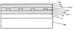
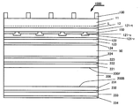
図1.A乃至図1.Kは、本発明の具体的な一実施例に係るIII族窒化物系化合物半導体発光素子1000の製造方法を示す工程図(断面図)である。尚、図1.K及び図2では、実質的に1チップのIII族窒化物系化合物半導体発光素子1000に対応する図を示しており、図1.A乃至図1.Jにおいても1チップ分の断面図に対応する図面を示している。しかし、図1.A乃至図1.Jは1枚のウエハ等の「一部」を拡大して表現したものであり、図1.Kも、ダイシング等によりチップ化する前の状態である1枚のウエハ等の「一部」を拡大した断面図をも意味するものである。
FIG. A to FIG. K is a process diagram (cross-sectional view) showing a method for manufacturing a group III nitride compound semiconductor
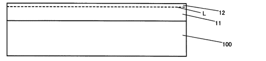
まず、サファイア基板100を用意し、通常のエピタキシャル成長によりIII族窒化物系化合物半導体層を形成する(図1.A)。図1.Aでは単純化して、n型層11とp型層12と発光領域Lとして積層されたIII族窒化物系化合物半導体層を示した。図1.A乃至図1.Kにおいて、n型層11とp型層12とは、破線で示した発光領域Lで接する2つの層の如く記載しているが、これらは細部の積層構造の記載を省略したものである。実際、サファイア基板100に例えばバッファ層、シリコンをドープしたGaNから成る高濃度n+層、GaNから成る低濃度n層、n−AlGaNクラッド層を構成するものであっても、図1.A乃至図1.Kにおいてはn型層11として代表させている。同様に、マグネシウムをドープしたp−AlGaNクラッド層、GaNから成る低濃度p層、GaNから成る高濃度p+層を構成するものであっても、図1.A乃至図1.Kにおいてはp型層12として代表させている。また、発光領域Lは、pn接合の場合の接合面と、例えば多重量子井戸構造の発光層(通常、井戸層はアンドープ層)の両方を代表して破線で示したものであり、単に「n型層11とp型層12との界面」を意味するものではない。但し、「発光領域の平面」は発光領域Lで示した破線付近に存在する、平面である。尚、p型層12は、下記の「窒素(N2)雰囲気下の熱処理」前においては、「p型不純物を含む層ではあるが、低抵抗化していない」ものであり、当該「窒素(N2)雰囲気下の熱処理」後においては、通常の意味の低抵抗のp型層である。
First, a
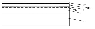
次に、電子ビーム蒸着により、p型層12の全面に厚さ300nmの酸化インジウムスズ(ITO)から成る透光性電極121−tを形成する。この後、N2雰囲気下、700℃で、5分間加熱処理してp型層12を低抵抗化すると共に、p型層12とITO電極121−tとの間のコンタクト抵抗を低抵抗化する。次に、ITO電極121−tの全面に、厚さ100nmの窒化ケイ素(SiNx)から成る誘電体層150を形成する(図1.B)。
Next, a translucent electrode 121-t made of indium tin oxide (ITO) having a thickness of 300 nm is formed on the entire surface of the p-
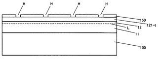
次に、図示しないレジスト膜を用いたフォトリソグラフにより、ドライエッチングでSiNxから成る誘電体層150に孔部Hを形成する。後述するように、孔部Hの形状と位置、即ちニッケル(Ni)から成る接続部121−cの形状と位置は、のちに形成する多層金属膜から成るn電極130の形状と位置との関係において、「発光領域Lの平面」に投影した両者の正射影が重ならないようにする。本実施例においては、孔部Hは、一辺400乃至500μmの正方形状のIII族窒化物系化合物半導体発光素子1000に対して幅約20μm、孔部Hの間隔80乃至100μmのストライプ状とした。この後レジスト膜を除去する(図1.C)。
Next, a hole H is formed in the
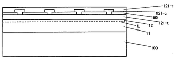
次に、孔部Hにニッケル(Ni)から成る接続部121−cを形成するため、図示しないレジスト膜を形成する。このレジスト膜には、SiNxから成る誘電体層150の孔部H上部に、当該孔部よりも大きい孔部を形成する。こうして、SiNxから成る誘電体層150の孔部Hと、その上に形成されたレジスト膜の孔部とにニッケル(Ni)を抵抗加熱蒸着により形成する。この際、ニッケル(Ni)はSiNxから成る誘電体層150の孔部Hを充填し、且つ誘電体層150上部に20nm厚の庇状部が形成されるまで蒸着した。こうして、レジスト膜を除去し、SiNxから成る誘電体層150の孔部Hを充填する、ニッケル(Ni)から成る接続部121−cを形成した(図1.D)。
Next, in order to form the connection part 121-c made of nickel (Ni) in the hole H, a resist film (not shown) is formed. In this resist film, a hole larger than the hole is formed above the hole H of the
次に、ニッケル(Ni)から成る接続部121−cを孔部Hに有するSiNxから成る誘電体層150の上に、厚さ300nmのアルミニウム(Al)から成る高反射性金属層121−rを蒸着により形成する(図1.E)。こうして、ITOから成る透光性電極121−t、ニッケル(Ni)から成る接続部121−c、アルミニウム(Al)から成る高反射性金属層121−rとにより、III族窒化物系化合物半導体層との密着性が高く、光を吸収せず高反射する、多重p電極が形成される。尚、ニッケル(Ni)から成る接続部121−cを孔部Hに有するSiNxから成る誘電体層150の役割は、アルミニウム(Al)とITOを直接接触させないことで、アルミニウム(Al)の酸化による電極特性の劣化を防止することである。
Next, the highly reflective metal layer 121-r made of aluminum (Al) having a thickness of 300 nm is formed on the
次に、多層金属膜を次の順に蒸着により形成する。厚さ50nmのチタン(Ti)層122、厚さ500nmのニッケル(Ni)層123、厚さ50nmの金(Au)層124。こうして図1.Fの層構成となる。チタン(Ti)層122、ニッケル(Ni)層123、金(Au)層124の機能は、次の通りである。スズ20%の金スズはんだ(Au−20Sn)51を設けるにあたって、当該金スズはんだ(Au−20Sn)51と合金化する層として金(Au)層124を、スズ(Sn)のアルミニウム(Al)から成る高反射性金属層121−rへの拡散を防ぐ層としてニッケル(Ni)層123を、ニッケル(Ni)層123とアルミニウム(Al)から成る高反射性金属層121−rとの密着性を向上させるためにチタン(Ti)層122を各々設けるものである。
Next, a multilayer metal film is formed by vapor deposition in the following order. A titanium (Ti)
次に金(Au)層124の上に、スズ20%の金スズはんだ(Au−20Sn)51を厚さ1500nm形成する(1.G)。
Next, a gold tin solder (Au-20Sn) 51 of 20% tin is formed on the gold (Au)
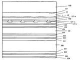
次にn型シリコン基板200を用意し、両面に導電性多層膜を次の順に蒸着等により形成する。表面側の層を符号221乃至224で、裏面側の層を符号231乃至244で示す。厚さ50nmの窒化チタン(TiN)層221及び231、厚さ100nmのチタン(Ti)層222及び232、厚さ500nmのニッケル(Ni)層223及び233、厚さ50nmの金(Au)層224及び234。窒化チタン(TiN)層221及び231は、n型シリコン基板200とのコンタクト抵抗が低い点から選択された層であり、チタン(Ti)層222及び232、ニッケル(Ni)層223及び233、金(Au)層224及び234の機能は、上述のチタン(Ti)層122、ニッケル(Ni)層123、金(Au)層124の機能と全く同様である。このn型シリコン基板200に形成した表面側の導電性多層膜の最上層である金(Au)層224の上にスズ20%の金スズはんだ(Au−20Sn)52を厚さ1500nm形成し、上述の図1.Gのスズ20%の金スズはんだ(Au−20Sn)51を厚さ1500nm形成したIII族窒化物系化合物半導体発光素子ウエハと、金スズはんだ(Au−20Sn)を形成した面同士を貼り合わせる(図1.H)。こうして、300℃、30kg重/cm2(2.94MPa)で熱プレスして、2つのウエハを合体させる。以下、金スズはんだ(Au−20Sn)は一体化した層50として示す(図1.I)。
Next, an n-
このような一体化されたウエハの、サファイア基板100側から、248nmのKrF高出力パルスレーザを照射する。照射条件は、0.7J/cm2以上、パルス幅25ns(ナノ秒)、照射領域2mm角又は3mm角で、各照射ごとに、レーザ照射領域外周が、「1チップ」を横切らないようにすると良い。このレーザ照射により、サファイア基板100に最も近いn型層11(GaN層)の界面11fが薄膜状に溶融し、ガリウム(Ga)液滴と窒素(N2)とに分解する。こののち、サファイア基板100を一体化ウエハからリフトオフにより除去する(図1.J)。この後、露出したn型層11表面を希塩酸により洗浄し、表面に付着しているガリウム(Ga)液滴を除去する。
The integrated wafer is irradiated with a 248 nm KrF high-power pulse laser from the
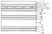
次に、図示しないレジスト膜を形成し、レジスト膜の孔部に多層金属膜から成るn電極130を次の順に蒸着により形成する。レジスト膜の孔部は、後述する通り、ニッケル(Ni)からなる接続部121−cの形状と正射影が互いに重ならないように「窓枠状」に形成した。次にn型層11の上(レジスト膜の孔部)に順に、厚さ15nmのバナジウム(V)層、厚さ150nmのアルミニウム(Al)層、厚さ30nmのチタン(Ti)層、厚さ500nmのニッケル(Ni)層、厚さ500nmの金(Au)層。この後にレジストをリフトオフして除去することで、レジスト膜の孔部の多層金属膜から成るn電極130が残り、他の領域の金属膜はレジストと共に除去される。こうして、両面に導電性多層膜を形成したn型シリコン基板200を支持基板とし、p側にITOから成る透光性電極121−t、ニッケル(Ni)から成る接続部121−c、アルミニウム(Al)から成る高反射性金属層121−rとを形成され、多層金属膜を介して金スズはんだ(Au−20Sn)50でn型シリコン基板200と電気的に接続された、III族窒化物系化合物半導体発光素子1000が形成された(図1.K)。III族窒化物系化合物半導体発光素子1000は、「窓枠状」に形成された多層金属膜から成るn電極130の形成されていない領域が光取り出し領域である発光素子である。
Next, a resist film (not shown) is formed, and an n-
この後、任意の方法で分割して個々の素子とする。例えばダイシングブレードによりハーフカットを行い、ブレーキングして分割する。ハーフカットは、シリコン基板200の裏面200Bからはシリコン基板200をある程度切削するようにする。一方、エピタキシャル層であるn型層11及びp型層12側は、少なくとも当該エピタキシャル層であるn型層11及びp型層12側が分割線付近で完全に切削されて分離されれば良く、必ずしもシリコン基板200の表面200Fにまで切削が達する必要は無い。
Thereafter, it is divided into arbitrary elements by an arbitrary method. For example, half cutting is performed with a dicing blade, and braking is performed for division. In the half cut, the
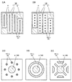
〔n電極130と、接続部121−cの充填された誘電体層150の孔部Hの平面形状について〕
n電極130と、接続部121−cの充填された誘電体層150の孔部Hの平面形状、即ち発光領域Lの平面への正射影は、重ならないことが望ましく、またそれらの正射影はいずれの位置においても一定の距離以下とならないことが好ましい。この場合の「一定の距離」とは、例えばn型層11とp型層12の総膜厚程度の距離、或いはその数倍を設定すると良い。例えばn型層11とp型層12の総膜厚が5μmであるならば、2つの正射影はいずれの位置においても5μm以上離れていることが望ましく、10μm以上離れていることがより望ましく、20μm以上離れていることが更に望ましい。
[About the planar shape of the hole H of the
It is desirable that the orthogonal projections of the n-
図2.Aは、例えば一辺が500μmのチップにおいて、n電極130を4つの窓の窓枠状に形成する例である。4つの窓wの幅を100μm、その窓枠であるストライプ状部分fの幅を20μmとする(右下がりのハッチング)。尚、図2.Aでは、n電極130のボンディング領域bとして、140μm角の正方形の領域を2箇所設ける例である。また、接続部121−cの充填された誘電体層150の孔部Hの平面形状は、n電極130の形成されていない4つの窓wの中心線に沿って、幅20μmのストライプ状に設ける(右上がりのハッチング)。こうして、n電極130と、接続部121−cの充填された誘電体層150の孔部Hの平面形状、即ち発光領域Lの平面への正射影は、重ならず、且ついずれの位置においても互いに20μm以上の間隔を有して離れている。このようにして、光取り出し領域(図2.Aで窓w)を確保しつつ、発光領域Lの全体を電流が通るようにできる。
FIG. A is an example in which the n-
図2.Aにおいて、接続部121−cの充填された誘電体層150の孔部Hの平面形状は、n電極130の形成されていない4つの窓wの中心線に沿って、幅20μmのストライプ状に設けたが、図2.Bのように、4つの窓wの中心線に沿って中心を有する、直径20μmの複数個の円状としても良い。或いは、n電極130(右下がりのハッチング)と接続部121−cの充填された誘電体層150の孔部H(右上がりのハッチング)の平面形状は、図2.C、図2.D、図2.Eのように様々に変形例を考案することができる。
FIG. In A, the planar shape of the hole H of the
上記実施例において、n電極130を直接n型層11に形成するのでなく、例えば透光性電極を形成したのちに更に窓枠状のn電極を形成しても良い。
In the above embodiment, the n-
1000:III族窒化物系化合物半導体発光素子
100:サファイア基板(エピタキシャル成長基板)
11:n型III族窒化物系化合物半導体層
12:p型III族窒化物系化合物半導体層
L:発光領域
121−t:ITOから成る透光性電極
121−c:Niから成る接続部
121−r:Alから成る高反射性金属層
200:シリコン基板(支持基板)
221、231:TiN層
122、222、232:Ti層
123、223、233:Ni層
124、224、234:Au層
130:多層金属膜から成るn電極
50、51、52:Au−20Snはんだ層
150:SiNxから成る誘電体層
H:誘電体層の孔部
1000: Group III nitride compound semiconductor light emitting device 100: Sapphire substrate (epitaxial growth substrate)
11: n-type group III nitride compound semiconductor layer 12: p-type group III nitride compound semiconductor layer L: Light emitting region 121-t: Translucent electrode made of ITO 121-c: Connection portion 121- made of Ni r: highly reflective metal layer made of Al 200: silicon substrate (support substrate)
221, 231:
Claims (4)
前記p層の上全面に形成された透光性電極と、
前記透光性電極の上全面に形成され、前記透光性電極に至る複数の孔を有した誘電体層と、
前記孔の周囲の誘電体層と接合し、前記孔に充填されて、前記透光性電極と接合した金属から成る接続部と、
前記接続部の前記誘電体層上に形成された部分の上及び前記誘電体層上の全面に形成された光反射性金属層と、
前記光反射性金属層上に一様に形成された接合層と、
前記接合層を介して前記光反射性金属層と接合する支持基板と、
前記成長基板が剥離されて露出した前記n層の表面上に形成されたn電極と、
を有し、
前記n層側から光を出力し、前記接続部と、前記n電極とは、前記発光層の発光領域の平面への正射影が互いに重ならない形状に形成されている
ことを特徴とするIII族窒化物系化合物半導体発光素子。 A group III nitride compound semiconductor is formed on a growth substrate, and at least an n layer, a light emitting layer, and an uppermost p layer are grown, and an electrode for the n layer and an electrode for the p layer are planar. In the group III nitride compound semiconductor light emitting device located on the upper side and the lower side across the light emitting region of
A translucent electrode formed on the entire upper surface of the p layer;
A dielectric layer formed on the entire upper surface of the translucent electrode and having a plurality of holes reaching the translucent electrode;
A connecting portion made of a metal bonded to the dielectric layer around the hole, filled in the hole, and bonded to the translucent electrode;
A light-reflective metal layer formed on a portion of the connection portion formed on the dielectric layer and on the entire surface of the dielectric layer;
A bonding layer uniformly formed on the light-reflecting metal layer;
A support substrate bonded to the light reflective metal layer via the bonding layer;
An n-electrode formed on the surface of the n-layer exposed by peeling off the growth substrate;
Have
Light is output from the n-layer side, and the connecting portion and the n-electrode are formed in a shape in which orthogonal projections onto the plane of the light-emitting region of the light-emitting layer do not overlap each other Nitride compound semiconductor light emitting device .
Priority Applications (1)
| Application Number | Priority Date | Filing Date | Title |
|---|---|---|---|
| JP2005352722A JP4920249B2 (en) | 2005-12-06 | 2005-12-06 | Group III nitride compound semiconductor light emitting device |
Applications Claiming Priority (1)
| Application Number | Priority Date | Filing Date | Title |
|---|---|---|---|
| JP2005352722A JP4920249B2 (en) | 2005-12-06 | 2005-12-06 | Group III nitride compound semiconductor light emitting device |
Publications (2)
| Publication Number | Publication Date |
|---|---|
| JP2007158128A JP2007158128A (en) | 2007-06-21 |
| JP4920249B2 true JP4920249B2 (en) | 2012-04-18 |
Family
ID=38242065
Family Applications (1)
| Application Number | Title | Priority Date | Filing Date |
|---|---|---|---|
| JP2005352722A Expired - Fee Related JP4920249B2 (en) | 2005-12-06 | 2005-12-06 | Group III nitride compound semiconductor light emitting device |
Country Status (1)
| Country | Link |
|---|---|
| JP (1) | JP4920249B2 (en) |
Families Citing this family (12)
| Publication number | Priority date | Publication date | Assignee | Title |
|---|---|---|---|---|
| JP2009231549A (en) * | 2008-03-24 | 2009-10-08 | Toyoda Gosei Co Ltd | Nitride-based semiconductor light-emitting device |
| KR101007099B1 (en) * | 2008-04-21 | 2011-01-10 | 엘지이노텍 주식회사 | Semiconductor light emitting device and manufacturing method thereof |
| JP5136398B2 (en) * | 2008-12-26 | 2013-02-06 | 豊田合成株式会社 | Group III nitride compound semiconductor light emitting device |
| JP2010171376A (en) | 2008-12-26 | 2010-08-05 | Toyoda Gosei Co Ltd | Group iii nitride-based compound semiconductor light-emitting device |
| TW201104913A (en) * | 2009-07-31 | 2011-02-01 | Tekcore Co Ltd | Vertical light-emitting diode and manufacture method thereof |
| JP2012175040A (en) | 2011-02-24 | 2012-09-10 | Toshiba Corp | Semiconductor light-emitting device and light-emitting apparatus |
| JP5949294B2 (en) * | 2011-08-31 | 2016-07-06 | 日亜化学工業株式会社 | Semiconductor light emitting device |
| JP2012142630A (en) * | 2012-04-27 | 2012-07-26 | Hitachi Cable Ltd | Light-emitting device |
| JP2012178610A (en) * | 2012-06-06 | 2012-09-13 | Toshiba Corp | Semiconductor light-emitting device and light-emitting apparatus |
| CN103682020A (en) * | 2012-08-31 | 2014-03-26 | 展晶科技(深圳)有限公司 | Manufacture method for LED (Light emitting diode) grain |
| JP6024506B2 (en) | 2013-02-18 | 2016-11-16 | 豊田合成株式会社 | Group III nitride semiconductor light emitting device and method for manufacturing the same |
| JP2013175761A (en) * | 2013-04-17 | 2013-09-05 | Toshiba Corp | Semiconductor light-emitting element and light-emitting apparatus |
Family Cites Families (6)
| Publication number | Priority date | Publication date | Assignee | Title |
|---|---|---|---|---|
| JP3511213B2 (en) * | 1994-03-30 | 2004-03-29 | スタンレー電気株式会社 | Optical semiconductor device |
| JP3765457B2 (en) * | 1999-01-08 | 2006-04-12 | 豊田合成株式会社 | Semiconductor element |
| JP3893874B2 (en) * | 1999-12-21 | 2007-03-14 | 日亜化学工業株式会社 | Manufacturing method of nitride semiconductor light emitting device |
| JP4411871B2 (en) * | 2003-06-17 | 2010-02-10 | 日亜化学工業株式会社 | Nitride semiconductor light emitting device |
| JP4604488B2 (en) * | 2003-12-26 | 2011-01-05 | 日亜化学工業株式会社 | Nitride semiconductor light emitting device and manufacturing method thereof |
| JP2007081011A (en) * | 2005-09-13 | 2007-03-29 | Matsushita Electric Ind Co Ltd | Semiconductor light emitting device |
-
2005
- 2005-12-06 JP JP2005352722A patent/JP4920249B2/en not_active Expired - Fee Related
Also Published As
| Publication number | Publication date |
|---|---|
| JP2007158128A (en) | 2007-06-21 |
Similar Documents
| Publication | Publication Date | Title |
|---|---|---|
| US20230197906A1 (en) | Semiconductor light emitting device | |
| CN101673794B (en) | Light emitting device | |
| JP5496104B2 (en) | Contact for semiconductor light emitting devices | |
| CN103999247B (en) | Light emitting diode and its manufacture method | |
| JP5304662B2 (en) | Light emitting element | |
| US20090294784A1 (en) | Nitride Semiconductor Light Emitting Element and Method for Producing Nitride Semiconductor Light Emitting Element | |
| JP2007158133A (en) | Method for producing group III nitride compound semiconductor device | |
| JP4920249B2 (en) | Group III nitride compound semiconductor light emitting device | |
| JP5729328B2 (en) | Group III nitride semiconductor light emitting device and method of manufacturing the same | |
| JP2008042143A (en) | Group iii nitride compound semiconductor light emitting element, and its manufacturing method | |
| JP4738999B2 (en) | Semiconductor optical device manufacturing method | |
| JP5298927B2 (en) | Light emitting element | |
| JP2007158131A (en) | Group III nitride compound semiconductor optical device | |
| KR20090115902A (en) | Vertical group III-nitride semiconductor light emitting diode device and manufacturing method | |
| JP4570683B2 (en) | Nitride compound semiconductor light emitting device manufacturing method | |
| JP2017069282A (en) | Semiconductor light-emitting element and method for manufacturing the same | |
| JP2010062355A (en) | Light-emitting device | |
| JP2007158132A (en) | Group III nitride compound semiconductor device and method for manufacturing the same | |
| JP2014120511A (en) | Method of manufacturing semiconductor device; and semiconductor device | |
| KR20090115631A (en) | Group III-nitride semiconductor light emitting diode device of vertical structure and manufacturing method | |
| JP2005347714A (en) | Light emitting device and its manufacturing method | |
| JP2007158130A (en) | Group iii nitride-based compound semiconductor optical element and manufacturing method thereof | |
| JP2022037340A (en) | Semiconductor light-emitting element | |
| JP2013172028A (en) | Semiconductor light-emitting element and vehicle lamp fitting | |
| JP2006319248A (en) | Nitride semiconductor light emitting device |
Legal Events
| Date | Code | Title | Description |
|---|---|---|---|
| A621 | Written request for application examination |
Free format text: JAPANESE INTERMEDIATE CODE: A621 Effective date: 20080618 |
|
| A977 | Report on retrieval |
Free format text: JAPANESE INTERMEDIATE CODE: A971007 Effective date: 20101130 |
|
| A131 | Notification of reasons for refusal |
Free format text: JAPANESE INTERMEDIATE CODE: A131 Effective date: 20111004 |
|
| A521 | Request for written amendment filed |
Free format text: JAPANESE INTERMEDIATE CODE: A523 Effective date: 20111201 |
|
| TRDD | Decision of grant or rejection written | ||
| A01 | Written decision to grant a patent or to grant a registration (utility model) |
Free format text: JAPANESE INTERMEDIATE CODE: A01 Effective date: 20120131 |
|
| A01 | Written decision to grant a patent or to grant a registration (utility model) |
Free format text: JAPANESE INTERMEDIATE CODE: A01 |
|
| A61 | First payment of annual fees (during grant procedure) |
Free format text: JAPANESE INTERMEDIATE CODE: A61 Effective date: 20120201 |
|
| R150 | Certificate of patent or registration of utility model |
Ref document number: 4920249 Country of ref document: JP Free format text: JAPANESE INTERMEDIATE CODE: R150 Free format text: JAPANESE INTERMEDIATE CODE: R150 |
|
| FPAY | Renewal fee payment (event date is renewal date of database) |
Free format text: PAYMENT UNTIL: 20150210 Year of fee payment: 3 |
|
| LAPS | Cancellation because of no payment of annual fees |