JP5905552B2 - トランスデューサおよびトランスデューサの製造方法 - Google Patents
トランスデューサおよびトランスデューサの製造方法 Download PDFInfo
- Publication number
- JP5905552B2 JP5905552B2 JP2014192851A JP2014192851A JP5905552B2 JP 5905552 B2 JP5905552 B2 JP 5905552B2 JP 2014192851 A JP2014192851 A JP 2014192851A JP 2014192851 A JP2014192851 A JP 2014192851A JP 5905552 B2 JP5905552 B2 JP 5905552B2
- Authority
- JP
- Japan
- Prior art keywords
- intermediate structure
- magnetic material
- magnetic
- recording
- transducer
- Prior art date
- Legal status (The legal status is an assumption and is not a legal conclusion. Google has not performed a legal analysis and makes no representation as to the accuracy of the status listed.)
- Active
Links
- 238000004519 manufacturing process Methods 0.000 title claims description 36
- 239000000696 magnetic material Substances 0.000 claims description 78
- 239000000463 material Substances 0.000 claims description 40
- 239000011241 protective layer Substances 0.000 claims description 39
- 239000000758 substrate Substances 0.000 claims description 29
- 238000010884 ion-beam technique Methods 0.000 claims description 16
- 238000000465 moulding Methods 0.000 claims description 16
- 238000000034 method Methods 0.000 claims description 13
- 239000011810 insulating material Substances 0.000 claims description 12
- 238000002513 implantation Methods 0.000 claims description 7
- 238000000151 deposition Methods 0.000 claims description 4
- 239000007943 implant Substances 0.000 claims 1
- 239000010410 layer Substances 0.000 description 35
- PNEYBMLMFCGWSK-UHFFFAOYSA-N aluminium oxide Inorganic materials [O-2].[O-2].[O-2].[Al+3].[Al+3] PNEYBMLMFCGWSK-UHFFFAOYSA-N 0.000 description 16
- 238000000992 sputter etching Methods 0.000 description 12
- 238000003860 storage Methods 0.000 description 11
- 230000007704 transition Effects 0.000 description 11
- 239000010949 copper Substances 0.000 description 8
- 230000015572 biosynthetic process Effects 0.000 description 5
- 230000004907 flux Effects 0.000 description 5
- 238000007493 shaping process Methods 0.000 description 5
- XKRFYHLGVUSROY-UHFFFAOYSA-N Argon Chemical compound [Ar] XKRFYHLGVUSROY-UHFFFAOYSA-N 0.000 description 4
- OKTJSMMVPCPJKN-UHFFFAOYSA-N Carbon Chemical compound [C] OKTJSMMVPCPJKN-UHFFFAOYSA-N 0.000 description 4
- RYGMFSIKBFXOCR-UHFFFAOYSA-N Copper Chemical compound [Cu] RYGMFSIKBFXOCR-UHFFFAOYSA-N 0.000 description 4
- KJTLSVCANCCWHF-UHFFFAOYSA-N Ruthenium Chemical compound [Ru] KJTLSVCANCCWHF-UHFFFAOYSA-N 0.000 description 4
- QVGXLLKOCUKJST-UHFFFAOYSA-N atomic oxygen Chemical compound [O] QVGXLLKOCUKJST-UHFFFAOYSA-N 0.000 description 4
- 229910052799 carbon Inorganic materials 0.000 description 4
- 238000006243 chemical reaction Methods 0.000 description 4
- 229910052802 copper Inorganic materials 0.000 description 4
- 238000005530 etching Methods 0.000 description 4
- 230000001939 inductive effect Effects 0.000 description 4
- 150000001247 metal acetylides Chemical class 0.000 description 4
- 150000004767 nitrides Chemical class 0.000 description 4
- 239000001301 oxygen Substances 0.000 description 4
- 229910052760 oxygen Inorganic materials 0.000 description 4
- 230000001681 protective effect Effects 0.000 description 4
- 229910052707 ruthenium Inorganic materials 0.000 description 4
- 229910052715 tantalum Inorganic materials 0.000 description 4
- GUVRBAGPIYLISA-UHFFFAOYSA-N tantalum atom Chemical compound [Ta] GUVRBAGPIYLISA-UHFFFAOYSA-N 0.000 description 4
- 229910002546 FeCo Inorganic materials 0.000 description 3
- QVYYOKWPCQYKEY-UHFFFAOYSA-N [Fe].[Co] Chemical compound [Fe].[Co] QVYYOKWPCQYKEY-UHFFFAOYSA-N 0.000 description 3
- 230000005415 magnetization Effects 0.000 description 3
- 229920002120 photoresistant polymer Polymers 0.000 description 3
- 229910052786 argon Inorganic materials 0.000 description 2
- 238000013500 data storage Methods 0.000 description 2
- 230000008021 deposition Effects 0.000 description 2
- 230000008030 elimination Effects 0.000 description 2
- 238000003379 elimination reaction Methods 0.000 description 2
- 230000007613 environmental effect Effects 0.000 description 2
- 238000003801 milling Methods 0.000 description 2
- 230000003647 oxidation Effects 0.000 description 2
- 238000007254 oxidation reaction Methods 0.000 description 2
- 125000006850 spacer group Chemical group 0.000 description 2
- 229910018072 Al 2 O 3 Inorganic materials 0.000 description 1
- 239000012141 concentrate Substances 0.000 description 1
- 230000000694 effects Effects 0.000 description 1
- 230000006872 improvement Effects 0.000 description 1
- 239000012212 insulator Substances 0.000 description 1
- 230000003993 interaction Effects 0.000 description 1
- 230000001172 regenerating effect Effects 0.000 description 1
- 239000000725 suspension Substances 0.000 description 1
Images


Classifications
-
- G—PHYSICS
- G11—INFORMATION STORAGE
- G11B—INFORMATION STORAGE BASED ON RELATIVE MOVEMENT BETWEEN RECORD CARRIER AND TRANSDUCER
- G11B5/00—Recording by magnetisation or demagnetisation of a record carrier; Reproducing by magnetic means; Record carriers therefor
- G11B5/127—Structure or manufacture of heads, e.g. inductive
- G11B5/31—Structure or manufacture of heads, e.g. inductive using thin films
- G11B5/3109—Details
- G11B5/3116—Shaping of layers, poles or gaps for improving the form of the electrical signal transduced, e.g. for shielding, contour effect, equalizing, side flux fringing, cross talk reduction between heads or between heads and information tracks
-
- G—PHYSICS
- G11—INFORMATION STORAGE
- G11B—INFORMATION STORAGE BASED ON RELATIVE MOVEMENT BETWEEN RECORD CARRIER AND TRANSDUCER
- G11B5/00—Recording by magnetisation or demagnetisation of a record carrier; Reproducing by magnetic means; Record carriers therefor
- G11B5/127—Structure or manufacture of heads, e.g. inductive
- G11B5/31—Structure or manufacture of heads, e.g. inductive using thin films
- G11B5/3103—Structure or manufacture of integrated heads or heads mechanically assembled and electrically connected to a support or housing
- G11B5/3106—Structure or manufacture of integrated heads or heads mechanically assembled and electrically connected to a support or housing where the integrated or assembled structure comprises means for conditioning against physical detrimental influence, e.g. wear, contamination
-
- G—PHYSICS
- G11—INFORMATION STORAGE
- G11B—INFORMATION STORAGE BASED ON RELATIVE MOVEMENT BETWEEN RECORD CARRIER AND TRANSDUCER
- G11B5/00—Recording by magnetisation or demagnetisation of a record carrier; Reproducing by magnetic means; Record carriers therefor
- G11B5/127—Structure or manufacture of heads, e.g. inductive
- G11B5/31—Structure or manufacture of heads, e.g. inductive using thin films
- G11B5/3163—Fabrication methods or processes specially adapted for a particular head structure, e.g. using base layers for electroplating, using functional layers for masking, using energy or particle beams for shaping the structure or modifying the properties of the basic layers
Landscapes
- Engineering & Computer Science (AREA)
- Manufacturing & Machinery (AREA)
- Magnetic Heads (AREA)
Description
典型的なデータ電子機器筐体は、さまざまな構成要素を封入する剛性のハウジングを含む。データ記憶システムは、電子機器筐体の一種である。データ記憶システムにおける構成要素として、1つ以上の記憶媒体が挙げられる。たとえば、記憶媒体は、媒体を回転させてディスクのデータ面が空力式軸受ヘッドスライダの下を通るようにするスピンドルモータ上に取付けられることができる。ヘッドスライダは、少なくとも1つのアームと、音声コイルモータから得られた機械的エネルギを用いて各媒体を横断する少なくとも1つの対応するサスペンションとを有するアクチュエータ上に支持される。スライダはトランスデューサを担持しており、このトランスデューサは、媒体のデータ面に情報を記録し、媒体のデータ面から情報を再生する。
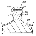
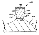
保護されたトランスデューサおよびその製造の実施例を開示する。トランスデューサの一実施例は、後縁と、前縁と、後縁および前縁の間に延びる1対の対向する側壁とを含むように成形される、基板上に形成された磁性材料を含む。保護材料の層は、成形された磁性材料の1対の側壁の各々と接触して位置決めされる。埋め戻し材料は、成形された磁性材料の1対の側壁の各々の上の保護材料を取囲む。
本開示の実施例は、磁気デバイスの製造中に生じ得る端縁反応ゾーンまたは不感層の排除または最小化に関する。磁気デバイスは、再生トランスデューサまたは記録トランスデューサなどの任意のタイプのトランスデューサに関連付けられることができる。しかしながら、本開示では、記録磁極の製造の例示的な実施例について特に説明する。
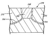
LD)で形成することができ、タンタル(Ta)、ルテニウム(Ru)、銅(Cu)、ダイヤモンド状炭素などの非磁性材料、または、アルミナもしくはさまざまな窒化物もしくは炭化物などの他の類似の材料を含み得る。図2に示される方法では、ステップ203および205は、真空を破壊することなく実行することができる。真空下でこれらのステップを実行することは、湿気および酸素に晒されることなどの環境条件に起因して側壁262および264が損傷を受けることを防ぐ。第1の保護層266が堆積されるとすぐに、磁性材料252が晒されることに関する問題が解消され、真空を破壊することができる。
Claims (2)
- トランスデューサの製造方法であって、
基板上に形成された磁性材料と、前記磁性材料上に堆積されたマスクとを含む第1の中間構造を得るステップと、
第2の中間構造を形成するために、イオンビーム打込みを用いて、第1のエネルギレベルで、前記第1の中間構造上で第1の成形作業を実行するステップとを備え、前記第2の中間構造における成形された磁性材料は、後縁と、前縁と、前記後縁および前記前縁の間に延びる1対の側壁とを含み、前記方法はさらに、
保護層を形成するために、前記第1のエネルギレベルよりも低い第2のエネルギレベルでのイオンビーム打込みを用いて、前記第2の中間構造における前記成形された磁性材料の前記側壁上に、前記側壁と接触して前記基板の材料を再堆積させるステップを備える、方法。 - トランスデューサの製造方法であって、
基板上に形成された磁性材料と、前記磁性材料上に堆積されたマスクとを含む第1の中間構造を得るステップを備え、前記構造を第1の部分と第2の部分とに分割する停止面が、前記磁性材料と前記マスクとの間に規定され、前記方法はさらに、
第2の中間構造を形成するために、前記第1の中間構造上で少なくとも1回の成形作業を実行するステップと、
第3の中間構造を形成するために、前記第2の中間構造上に非磁性材料からなる第1の保護層を堆積させるステップと、
第4の中間構造を形成するために、絶縁材料で前記第3の中間構造を埋め戻しするステップと、
第5の中間構造を形成するために、埋め戻しされた絶縁材料の一部、前記マスクの全体および前記第1の保護層の一部を含む前記構造の前記第1の部分を前記停止面において除去するステップとを備える、方法。
Applications Claiming Priority (2)
| Application Number | Priority Date | Filing Date | Title |
|---|---|---|---|
| US12/502,179 | 2009-07-13 | ||
| US12/502,179 US9058823B2 (en) | 2009-07-13 | 2009-07-13 | Protected transducer for dead layer reduction |
Related Parent Applications (1)
| Application Number | Title | Priority Date | Filing Date |
|---|---|---|---|
| JP2010158107A Division JP5675192B2 (ja) | 2009-07-13 | 2010-07-12 | トランスデューサおよびトランスデューサの製造方法 |
Publications (2)
| Publication Number | Publication Date |
|---|---|
| JP2014238911A JP2014238911A (ja) | 2014-12-18 |
| JP5905552B2 true JP5905552B2 (ja) | 2016-04-20 |
Family
ID=43427285
Family Applications (2)
| Application Number | Title | Priority Date | Filing Date |
|---|---|---|---|
| JP2010158107A Expired - Fee Related JP5675192B2 (ja) | 2009-07-13 | 2010-07-12 | トランスデューサおよびトランスデューサの製造方法 |
| JP2014192851A Active JP5905552B2 (ja) | 2009-07-13 | 2014-09-22 | トランスデューサおよびトランスデューサの製造方法 |
Family Applications Before (1)
| Application Number | Title | Priority Date | Filing Date |
|---|---|---|---|
| JP2010158107A Expired - Fee Related JP5675192B2 (ja) | 2009-07-13 | 2010-07-12 | トランスデューサおよびトランスデューサの製造方法 |
Country Status (3)
| Country | Link |
|---|---|
| US (1) | US9058823B2 (ja) |
| JP (2) | JP5675192B2 (ja) |
| CN (1) | CN101996642B (ja) |
Families Citing this family (2)
| Publication number | Priority date | Publication date | Assignee | Title |
|---|---|---|---|---|
| US20100108636A1 (en) * | 2008-10-30 | 2010-05-06 | Seagate Technology Llc | Integrated Tool for Fabricating an Electronic Component |
| KR102411080B1 (ko) * | 2015-09-02 | 2022-06-21 | 삼성전자주식회사 | 패턴 형성 방법 및 이를 이용한 자기 메모리 장치의 제조 방법 |
Family Cites Families (26)
| Publication number | Priority date | Publication date | Assignee | Title |
|---|---|---|---|---|
| US5734531A (en) * | 1995-10-31 | 1998-03-31 | Quantum Peripherals Colorado, Inc. | Magneto-resistive read/write head having a combination pole/shield |
| US6264848B1 (en) * | 1998-04-09 | 2001-07-24 | Seagate Technology Llc | Method for providing track position and identification information for data storage devices |
| US6519119B1 (en) * | 1999-11-03 | 2003-02-11 | Seagate Technology, Llc | Structure for current perrpendicular to plane giant magnetoresistive read heads |
| JP2002367112A (ja) * | 2001-06-08 | 2002-12-20 | Tdk Corp | 薄膜磁気ヘッドの製造方法 |
| US6687085B2 (en) | 2001-07-17 | 2004-02-03 | Seagate Technology Llc | Perpendicular write head with high magnetization pole material and method of fabricating the write head |
| JP2003298139A (ja) | 2002-03-29 | 2003-10-17 | Alps Electric Co Ltd | 磁気検出素子 |
| JP2003332649A (ja) | 2002-05-14 | 2003-11-21 | Alps Electric Co Ltd | 磁気検出素子 |
| US6998061B1 (en) | 2002-09-06 | 2006-02-14 | Maxtor Corporation | In-situ exchange biased GMR head for ultra-high density recording with pinning layer-only anneal |
| US7292409B1 (en) | 2004-02-27 | 2007-11-06 | Western Digital (Fremont), Llc | Magnetic head with thin trailing pedestal layer |
| US7367110B2 (en) | 2004-09-27 | 2008-05-06 | Hitachi Global Storage Technologies Netherlands B.V. | Method of fabricating a read head having shaped read sensor-biasing layer junctions using partial milling |
| US7228619B2 (en) | 2004-10-29 | 2007-06-12 | Hitachi Global Storage Technologies Netherlands B.V. | Method of manufacturing a magnetic head with common seed layer for coil and pedestal |
| JP2006134507A (ja) * | 2004-11-08 | 2006-05-25 | Tdk Corp | 磁気ヘッドの製造方法、磁気ヘッド、ヘッドジンバルアセンブリ、ヘッドアームアセンブリ、ヘッドスタックアセンブリ |
| US7639456B2 (en) | 2005-10-06 | 2009-12-29 | Hitachi Global Storage Technologies Netherlands B.V. | Double mill process for patterning current perpendicular to plane (CPP) magnetoresistive devices to minimize barrier shorting and barrier damage |
| US7446984B2 (en) | 2005-12-14 | 2008-11-04 | Hitachi Global Storage Technologies Netherlands B.V. | Magnetic random access memory (MRAM) having increased reference layer anisotropy through ion beam etch of magnetic layers |
| JP2007184022A (ja) | 2006-01-04 | 2007-07-19 | Alps Electric Co Ltd | 垂直磁気記録ヘッドの主磁極形成方法 |
| US20070183093A1 (en) | 2006-02-07 | 2007-08-09 | Quang Le | Protective layer for CMP assisted lift-off process and method of fabrication |
| JP2007257775A (ja) * | 2006-03-24 | 2007-10-04 | Tdk Corp | 狭幅の下部層を有する薄膜素子の製造方法及び該素子を備えた薄膜磁気ヘッド |
| US7765677B2 (en) | 2006-04-18 | 2010-08-03 | Hitachi Global Storage Technologies Netherlands B.V. | Method for manufacturing a magnetic write head using a protective layer to prevent write pole consumption |
| US7748103B2 (en) * | 2006-04-24 | 2010-07-06 | Hitachi Global Storage Technologies Netherlands B.V. | Method of manufacturing a perpendicular magnetic recording write head with notched trailing shield |
| US7587811B2 (en) | 2006-04-25 | 2009-09-15 | Hitachi Global Storage Technologies Netherlands B.V. | Method for manufacturing a magnetic write head for perpendicular magnetic data recording |
| JP2008052840A (ja) | 2006-08-25 | 2008-03-06 | Hitachi Global Storage Technologies Netherlands Bv | 磁気ヘッドスライダの製造方法 |
| US7578049B2 (en) | 2006-09-21 | 2009-08-25 | Hitachi Global Storage Technologies Netherlands B.V. | Method for constructing a magnetic write pole for a perpendicular magnetic recording head |
| US7715147B2 (en) | 2006-10-27 | 2010-05-11 | Hitachi Global Storage Technologies Netherlands B.V. | Magnetic write head having a shield that extends below the leading edge of the write pole |
| US7993535B2 (en) * | 2007-01-26 | 2011-08-09 | International Business Machines Corporation | Robust self-aligned process for sub-65nm current-perpendicular junction pillars |
| JP2008210481A (ja) | 2007-02-27 | 2008-09-11 | Fujitsu Ltd | 磁気記録装置の製造方法 |
| US20100108636A1 (en) * | 2008-10-30 | 2010-05-06 | Seagate Technology Llc | Integrated Tool for Fabricating an Electronic Component |
-
2009
- 2009-07-13 US US12/502,179 patent/US9058823B2/en active Active
-
2010
- 2010-07-12 JP JP2010158107A patent/JP5675192B2/ja not_active Expired - Fee Related
- 2010-07-13 CN CN 201010278034 patent/CN101996642B/zh not_active Expired - Fee Related
-
2014
- 2014-09-22 JP JP2014192851A patent/JP5905552B2/ja active Active
Also Published As
| Publication number | Publication date |
|---|---|
| CN101996642B (zh) | 2013-06-05 |
| US9058823B2 (en) | 2015-06-16 |
| JP2014238911A (ja) | 2014-12-18 |
| US20110007422A1 (en) | 2011-01-13 |
| JP5675192B2 (ja) | 2015-02-25 |
| CN101996642A (zh) | 2011-03-30 |
| JP2011023101A (ja) | 2011-02-03 |
Similar Documents
| Publication | Publication Date | Title |
|---|---|---|
| JP4999121B2 (ja) | サイドシールド層を有する垂直磁気記録用磁気ヘッドおよびその製造方法 | |
| US5809636A (en) | Method of making a magnetoresistive thin film magnetic head with specific shapes of leads | |
| US7388732B2 (en) | Perpendicular recording magnetic head with a write shield megnetically coupled to a first pole piece | |
| US6433968B1 (en) | Merged read/write head and method of fabricating same | |
| KR100924695B1 (ko) | 수직 자기 기록 헤드 및 그 제조방법 | |
| US6999277B2 (en) | Magnetic head having thermally assisted write head with heater element, and protective sacrificial layer | |
| JP2007128581A (ja) | 磁気ヘッド及びその製造方法 | |
| JP3817223B2 (ja) | 薄膜磁気ヘッド及びその製造方法 | |
| US6665156B2 (en) | Magnetoresistive head, manufacture thereof, and magnetic recording/reproducing apparatus with such magnetic head | |
| JP2002329905A (ja) | Cpp構造磁気抵抗効果素子およびその製造方法 | |
| JP5905552B2 (ja) | トランスデューサおよびトランスデューサの製造方法 | |
| CN100349210C (zh) | 磁头及其制造方法 | |
| JP2008192269A (ja) | 磁気リード・ヘッド及びその製造方法 | |
| JP2005182897A (ja) | 薄膜磁気ヘッドおよびその製造方法 | |
| US10950261B2 (en) | Supermalloy and MU metal side and top shields for magnetic read heads | |
| KR100617282B1 (ko) | Cpp 구조 자기 저항 효과 소자 | |
| JPH10154312A (ja) | 磁気ヘッド及びその製造方法 | |
| JP3902183B2 (ja) | 磁気ヘッドおよびその製造方法ならびに磁気記録再生装置 | |
| US6404588B1 (en) | Thin film magnetic head having magnetic yoke layer connected to magnetic yoke piece of reduced width | |
| JP3639529B2 (ja) | 薄膜磁気ヘッド及び薄膜磁気ヘッドの製造方法 | |
| JPH10283617A (ja) | 垂直磁気記録用複合型ヘッド | |
| JP2009205710A (ja) | 垂直磁気記録ヘッドおよびその製造方法 | |
| JP2000215411A (ja) | 薄膜磁気ヘッド、並びに、その製造方法 | |
| JP2008140521A (ja) | 磁気ヘッドおよびその製造方法 | |
| JP2007026562A (ja) | 薄膜磁気ヘッドおよびその製造方法 |
Legal Events
| Date | Code | Title | Description |
|---|---|---|---|
| A621 | Written request for application examination |
Free format text: JAPANESE INTERMEDIATE CODE: A621 Effective date: 20141014 |
|
| A977 | Report on retrieval |
Free format text: JAPANESE INTERMEDIATE CODE: A971007 Effective date: 20150615 |
|
| A131 | Notification of reasons for refusal |
Free format text: JAPANESE INTERMEDIATE CODE: A131 Effective date: 20150707 |
|
| A601 | Written request for extension of time |
Free format text: JAPANESE INTERMEDIATE CODE: A601 Effective date: 20151006 |
|
| A521 | Written amendment |
Free format text: JAPANESE INTERMEDIATE CODE: A523 Effective date: 20151102 |
|
| TRDD | Decision of grant or rejection written | ||
| A01 | Written decision to grant a patent or to grant a registration (utility model) |
Free format text: JAPANESE INTERMEDIATE CODE: A01 Effective date: 20160216 |
|
| A61 | First payment of annual fees (during grant procedure) |
Free format text: JAPANESE INTERMEDIATE CODE: A61 Effective date: 20160316 |
|
| R150 | Certificate of patent or registration of utility model |
Ref document number: 5905552 Country of ref document: JP Free format text: JAPANESE INTERMEDIATE CODE: R150 |
|
| R250 | Receipt of annual fees |
Free format text: JAPANESE INTERMEDIATE CODE: R250 |
|
| R250 | Receipt of annual fees |
Free format text: JAPANESE INTERMEDIATE CODE: R250 |