JP5905552B2 - Transducer and transducer manufacturing method - Google Patents
Transducer and transducer manufacturing method Download PDFInfo
- Publication number
- JP5905552B2 JP5905552B2 JP2014192851A JP2014192851A JP5905552B2 JP 5905552 B2 JP5905552 B2 JP 5905552B2 JP 2014192851 A JP2014192851 A JP 2014192851A JP 2014192851 A JP2014192851 A JP 2014192851A JP 5905552 B2 JP5905552 B2 JP 5905552B2
- Authority
- JP
- Japan
- Prior art keywords
- intermediate structure
- magnetic material
- magnetic
- recording
- transducer
- Prior art date
- Legal status (The legal status is an assumption and is not a legal conclusion. Google has not performed a legal analysis and makes no representation as to the accuracy of the status listed.)
- Active
Links
- 238000004519 manufacturing process Methods 0.000 title claims description 36
- 239000000696 magnetic material Substances 0.000 claims description 78
- 239000000463 material Substances 0.000 claims description 40
- 239000011241 protective layer Substances 0.000 claims description 39
- 239000000758 substrate Substances 0.000 claims description 29
- 238000010884 ion-beam technique Methods 0.000 claims description 16
- 238000000465 moulding Methods 0.000 claims description 16
- 238000000034 method Methods 0.000 claims description 13
- 239000011810 insulating material Substances 0.000 claims description 12
- 238000002513 implantation Methods 0.000 claims description 7
- 238000000151 deposition Methods 0.000 claims description 4
- 239000007943 implant Substances 0.000 claims 1
- 239000010410 layer Substances 0.000 description 35
- PNEYBMLMFCGWSK-UHFFFAOYSA-N aluminium oxide Inorganic materials [O-2].[O-2].[O-2].[Al+3].[Al+3] PNEYBMLMFCGWSK-UHFFFAOYSA-N 0.000 description 16
- 238000000992 sputter etching Methods 0.000 description 12
- 238000003860 storage Methods 0.000 description 11
- 230000007704 transition Effects 0.000 description 11
- 239000010949 copper Substances 0.000 description 8
- 230000015572 biosynthetic process Effects 0.000 description 5
- 230000004907 flux Effects 0.000 description 5
- 238000007493 shaping process Methods 0.000 description 5
- XKRFYHLGVUSROY-UHFFFAOYSA-N Argon Chemical compound [Ar] XKRFYHLGVUSROY-UHFFFAOYSA-N 0.000 description 4
- OKTJSMMVPCPJKN-UHFFFAOYSA-N Carbon Chemical compound [C] OKTJSMMVPCPJKN-UHFFFAOYSA-N 0.000 description 4
- RYGMFSIKBFXOCR-UHFFFAOYSA-N Copper Chemical compound [Cu] RYGMFSIKBFXOCR-UHFFFAOYSA-N 0.000 description 4
- KJTLSVCANCCWHF-UHFFFAOYSA-N Ruthenium Chemical compound [Ru] KJTLSVCANCCWHF-UHFFFAOYSA-N 0.000 description 4
- QVGXLLKOCUKJST-UHFFFAOYSA-N atomic oxygen Chemical compound [O] QVGXLLKOCUKJST-UHFFFAOYSA-N 0.000 description 4
- 229910052799 carbon Inorganic materials 0.000 description 4
- 238000006243 chemical reaction Methods 0.000 description 4
- 229910052802 copper Inorganic materials 0.000 description 4
- 238000005530 etching Methods 0.000 description 4
- 230000001939 inductive effect Effects 0.000 description 4
- 150000001247 metal acetylides Chemical class 0.000 description 4
- 150000004767 nitrides Chemical class 0.000 description 4
- 239000001301 oxygen Substances 0.000 description 4
- 229910052760 oxygen Inorganic materials 0.000 description 4
- 230000001681 protective effect Effects 0.000 description 4
- 229910052707 ruthenium Inorganic materials 0.000 description 4
- 229910052715 tantalum Inorganic materials 0.000 description 4
- GUVRBAGPIYLISA-UHFFFAOYSA-N tantalum atom Chemical compound [Ta] GUVRBAGPIYLISA-UHFFFAOYSA-N 0.000 description 4
- 229910002546 FeCo Inorganic materials 0.000 description 3
- QVYYOKWPCQYKEY-UHFFFAOYSA-N [Fe].[Co] Chemical compound [Fe].[Co] QVYYOKWPCQYKEY-UHFFFAOYSA-N 0.000 description 3
- 230000005415 magnetization Effects 0.000 description 3
- 229920002120 photoresistant polymer Polymers 0.000 description 3
- 229910052786 argon Inorganic materials 0.000 description 2
- 238000013500 data storage Methods 0.000 description 2
- 230000008021 deposition Effects 0.000 description 2
- 230000008030 elimination Effects 0.000 description 2
- 238000003379 elimination reaction Methods 0.000 description 2
- 230000007613 environmental effect Effects 0.000 description 2
- 238000003801 milling Methods 0.000 description 2
- 230000003647 oxidation Effects 0.000 description 2
- 238000007254 oxidation reaction Methods 0.000 description 2
- 125000006850 spacer group Chemical group 0.000 description 2
- 229910018072 Al 2 O 3 Inorganic materials 0.000 description 1
- 239000012141 concentrate Substances 0.000 description 1
- 230000000694 effects Effects 0.000 description 1
- 230000006872 improvement Effects 0.000 description 1
- 239000012212 insulator Substances 0.000 description 1
- 230000003993 interaction Effects 0.000 description 1
- 230000001172 regenerating effect Effects 0.000 description 1
- 239000000725 suspension Substances 0.000 description 1
Images


Classifications
-
- G—PHYSICS
- G11—INFORMATION STORAGE
- G11B—INFORMATION STORAGE BASED ON RELATIVE MOVEMENT BETWEEN RECORD CARRIER AND TRANSDUCER
- G11B5/00—Recording by magnetisation or demagnetisation of a record carrier; Reproducing by magnetic means; Record carriers therefor
- G11B5/127—Structure or manufacture of heads, e.g. inductive
- G11B5/31—Structure or manufacture of heads, e.g. inductive using thin films
- G11B5/3109—Details
- G11B5/3116—Shaping of layers, poles or gaps for improving the form of the electrical signal transduced, e.g. for shielding, contour effect, equalizing, side flux fringing, cross talk reduction between heads or between heads and information tracks
-
- G—PHYSICS
- G11—INFORMATION STORAGE
- G11B—INFORMATION STORAGE BASED ON RELATIVE MOVEMENT BETWEEN RECORD CARRIER AND TRANSDUCER
- G11B5/00—Recording by magnetisation or demagnetisation of a record carrier; Reproducing by magnetic means; Record carriers therefor
- G11B5/127—Structure or manufacture of heads, e.g. inductive
- G11B5/31—Structure or manufacture of heads, e.g. inductive using thin films
- G11B5/3103—Structure or manufacture of integrated heads or heads mechanically assembled and electrically connected to a support or housing
- G11B5/3106—Structure or manufacture of integrated heads or heads mechanically assembled and electrically connected to a support or housing where the integrated or assembled structure comprises means for conditioning against physical detrimental influence, e.g. wear, contamination
-
- G—PHYSICS
- G11—INFORMATION STORAGE
- G11B—INFORMATION STORAGE BASED ON RELATIVE MOVEMENT BETWEEN RECORD CARRIER AND TRANSDUCER
- G11B5/00—Recording by magnetisation or demagnetisation of a record carrier; Reproducing by magnetic means; Record carriers therefor
- G11B5/127—Structure or manufacture of heads, e.g. inductive
- G11B5/31—Structure or manufacture of heads, e.g. inductive using thin films
- G11B5/3163—Fabrication methods or processes specially adapted for a particular head structure, e.g. using base layers for electroplating, using functional layers for masking, using energy or particle beams for shaping the structure or modifying the properties of the basic layers
Landscapes
- Engineering & Computer Science (AREA)
- Manufacturing & Machinery (AREA)
- Magnetic Heads (AREA)
Description
背景
典型的なデータ電子機器筐体は、さまざまな構成要素を封入する剛性のハウジングを含む。データ記憶システムは、電子機器筐体の一種である。データ記憶システムにおける構成要素として、1つ以上の記憶媒体が挙げられる。たとえば、記憶媒体は、媒体を回転させてディスクのデータ面が空力式軸受ヘッドスライダの下を通るようにするスピンドルモータ上に取付けられることができる。ヘッドスライダは、少なくとも1つのアームと、音声コイルモータから得られた機械的エネルギを用いて各媒体を横断する少なくとも1つの対応するサスペンションとを有するアクチュエータ上に支持される。スライダはトランスデューサを担持しており、このトランスデューサは、媒体のデータ面に情報を記録し、媒体のデータ面から情報を再生する。
BACKGROUND A typical data electronics housing includes a rigid housing that encloses various components. A data storage system is a type of electronic device casing. A component in a data storage system includes one or more storage media. For example, the storage medium can be mounted on a spindle motor that rotates the medium so that the data surface of the disk passes under the aerodynamic bearing head slider. The head slider is supported on an actuator having at least one arm and at least one corresponding suspension that traverses each medium using mechanical energy obtained from a voice coil motor. The slider carries a transducer, which records information on the data side of the medium and reproduces information from the data side of the medium.
媒体の面密度を大きくする必要性が果てしないため、トランスデューサの大きさは絶えず縮小している。たとえば、再生センサおよび記録磁極などの磁気トランスデューサの幅は、媒体上のより小さなトラックサイズに合わせるために、より小さくなっている。 Since the need for increasing the areal density of the medium is ending, the size of the transducer is constantly shrinking. For example, the width of magnetic transducers such as read sensors and recording poles are smaller to accommodate smaller track sizes on the media.
一般に、再生センサも記録磁極も、イオンビームエッチング(ion beam etching)(IBE)などのいくつかのタイプのイオンミリングによって規定される。しかしながら、再生センサおよび記録磁極が規定された後、デバイスの側面では、制御されない厚みを有する反応ゾーンまたは不感層(dead layer)の形成が生じる。 In general, both the read sensor and the recording pole are defined by several types of ion milling, such as ion beam etching (IBE). However, after the read sensor and recording pole are defined, the side of the device results in the formation of a reaction zone or dead layer with an uncontrolled thickness.
不感層の形成は、さまざまな理由によって引き起こされる可能性がある。たとえば、イオンミリング中にデバイスの側壁に打込まれるアルゴンビームは、イオンにより誘発される物理的損傷を引き起こす可能性がある。別の例では、再生センサまたは記録磁極がイオンミリングによって規定された後、イオンミリング処理されたデバイスは、他の製造プロセスに遷移するための雰囲気に晒される。イオンミリング処理されたばかりのデバイスが雰囲気に晒されるために、酸素および水分が容易にデバイスの端縁と反応し得る。さらに別の例では、側壁に対するその後の酸化が、アルミナ硬質マスクまたは他のアルミナ層から生じ得る。 The formation of the dead layer can be caused by various reasons. For example, an argon beam that is implanted into the device sidewall during ion milling can cause ion-induced physical damage. In another example, after the read sensor or recording pole is defined by ion milling, the ion milled device is exposed to an atmosphere for transition to another manufacturing process. Because the device that has just been ion milled is exposed to the atmosphere, oxygen and moisture can easily react with the edge of the device. In yet another example, subsequent oxidation to the sidewalls can result from an alumina hard mask or other alumina layer.
不感層は、減少した磁気モーメントをデバイスに提供する。記録磁極の場合には、不感層は、不感層をもたない記録磁極と比較して、より湾曲した遷移を記録磁極に記録させる可能性がある。再生部の場合には、デバイスの抵抗は不感層の厚みによって異なる可能性があるため、再生部の端縁効果が不可欠である。記録磁極および再生部における端縁反応ゾーンの制御または排除は、再生部/記録部の性能制御にとって重要である。 The dead layer provides the device with a reduced magnetic moment. In the case of a recording pole, the dead layer may cause the recording pole to record a more curved transition compared to a recording pole without a dead layer. In the case of the reproducing part, the resistance of the device may vary depending on the thickness of the insensitive layer, so the edge effect of the reproducing part is indispensable. Control or elimination of the edge reaction zone in the recording pole and playback section is important for playback / recorder performance control.
上記の説明は、単に一般的な背景情報のためになされているに過ぎず、クレームされる主題の範囲の決定を助けるものとして用いられることを意図していない。 The above description is merely for general background information and is not intended to be used as an aid in determining the scope of the claimed subject matter.
概要
保護されたトランスデューサおよびその製造の実施例を開示する。トランスデューサの一実施例は、後縁と、前縁と、後縁および前縁の間に延びる1対の対向する側壁とを含むように成形される、基板上に形成された磁性材料を含む。保護材料の層は、成形された磁性材料の1対の側壁の各々と接触して位置決めされる。埋め戻し材料は、成形された磁性材料の1対の側壁の各々の上の保護材料を取囲む。
SUMMARY Disclosed are embodiments of protected transducers and their manufacture. One example of a transducer includes a magnetic material formed on a substrate that is shaped to include a trailing edge, a leading edge, and a pair of opposing sidewalls extending between the trailing and leading edges. The layer of protective material is positioned in contact with each of the pair of side walls of the molded magnetic material. The backfill material surrounds the protective material on each of the pair of side walls of the molded magnetic material.
トランスデューサの一実施例を製造するために、基板上に形成された磁性材料と、磁性材料上に堆積されたマスクとを含む第1の中間構造が得られる。当該構造を第1の部分と第2の部分とに分割する停止面が、磁性材料とマスクとの間に規定される。第2の中間構造を形成するために、第1の中間構造上で少なくとも1回の成形作業が実行される。第3の中間構造を形成するために、第2の中間構造上に非磁性材料からなる第1の保護層が堆積される。第4の中間構造を形成するために、絶縁材料で第3の中間構造が埋め戻しされる。第5の中間構造を形成するために、埋め戻しされた絶縁材料の一部、マスクおよび第1の保護層の一部を含む構造の第1の部分が停止面において除去される。 To manufacture an embodiment of the transducer, a first intermediate structure is obtained that includes a magnetic material formed on a substrate and a mask deposited on the magnetic material. A stop surface that divides the structure into a first portion and a second portion is defined between the magnetic material and the mask. At least one molding operation is performed on the first intermediate structure to form the second intermediate structure. To form a third intermediate structure, a first protective layer made of a nonmagnetic material is deposited on the second intermediate structure. To form the fourth intermediate structure, the third intermediate structure is backfilled with an insulating material. To form a fifth intermediate structure, a first portion of the structure including a portion of the backfilled insulating material, a mask, and a portion of the first protective layer is removed at the stop surface.
トランスデューサの別の実施例を製造するために、基板上に形成された磁性材料と、磁性材料上に堆積されたマスクとを含む第1の中間構造が得られる。第2の中間構造を形成するために、イオンビーム打込みを用いて、第1のエネルギレベルで、第1の中間構造上での第1の成形作業が実行される。保護層を形成するために、イオンビーム打込みを用いて、第2の中間構造における成形された磁性材料の側壁上に、側壁と接触して基板の材料が再堆積される。 To manufacture another embodiment of the transducer, a first intermediate structure is obtained that includes a magnetic material formed on a substrate and a mask deposited on the magnetic material. To form the second intermediate structure, a first shaping operation is performed on the first intermediate structure at a first energy level using ion beam implantation. To form the protective layer, ion beam implantation is used to redeposit the substrate material on the sidewalls of the shaped magnetic material in the second intermediate structure in contact with the sidewalls.
これらのならびにさまざまな他の特徴および利点は、以下の詳細な説明を読むことによって明らかである。この概要は、クレームされる主題の鍵となる特徴または不可欠な特徴を特定することを意図しているわけではなく、クレームされる主題の範囲の決定を助けるものとして用いられることを意図しているわけでもない。クレームされる主題は、背景に記載された任意のまたはすべての不利な点を解決する実現例に限定されない。 These as well as various other features and advantages will be apparent upon reading the following detailed description. This summary is not intended to identify key or essential features of the claimed subject matter, but is intended to be used as an aid in determining the scope of the claimed subject matter. That's not true. The claimed subject matter is not limited to implementations that solve any or all disadvantages noted in the background.
詳細な説明
本開示の実施例は、磁気デバイスの製造中に生じ得る端縁反応ゾーンまたは不感層の排除または最小化に関する。磁気デバイスは、再生トランスデューサまたは記録トランスデューサなどの任意のタイプのトランスデューサに関連付けられることができる。しかしながら、本開示では、記録磁極の製造の例示的な実施例について特に説明する。
Detailed Description Embodiments of the present disclosure relate to the elimination or minimization of edge reaction zones or dead layers that may occur during the manufacture of magnetic devices. The magnetic device can be associated with any type of transducer, such as a reproduction transducer or a recording transducer. However, this disclosure specifically describes exemplary embodiments of recording pole manufacturing.
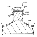
図1は、媒体104への垂直磁気記録のための例示的な再生/記録トランスデューサ102の部分断面図を示す。図1では、明確にするために、すべての間隔層および絶縁層を省略している。再生/記録トランスデューサ102は、スライダ(図1には図示せず)の後縁に形成された記録素子106と再生素子108とを含む。再生素子108は、上部シールド112と下部シールド114との間に間隔をおいて配置された再生センサ110を含む。上部シールド112および下部シールド114は、媒体104に記録されたデータのビットを検知することに影響を及ぼし得るであろう外部磁場から再生センサ110を隔離するように動作する。
FIG. 1 shows a partial cross-sectional view of an exemplary read / write
記録素子106は、記録磁極115と、第1の戻り磁極118と、第2の戻り磁極119とを含む。記録磁極115は、記録磁極先端部126を有する主要部116を含む。磁極先端部126は、後縁148と、前縁149とを含む。記録磁極115は、また、ヨーク部117を含む。第1の戻り磁極118は、第1の戻り磁極先端部128を含み、第1のスペーサ120によって記録磁極115から切離されている。第1の戻り磁極118は、第1の後部間隙閉鎖部122において記録磁極115に接続されている。第1の戻り磁極118は、記録磁極先端部126の前縁149から間隔をおいて配置されている。第2の戻り磁極119は、記録磁極115の、第1の戻り磁極118とは反対側に位置決めされている。特に、第2の戻り磁極119は、記録磁極先端部126の後縁148から間隔をおいて配置されている。第2の戻り磁極先端部129を有する第2の戻り磁極119は、第2のスペーサ121によって記録磁極115から切離され、第2の後部間隙閉鎖部123において接続されている。主要磁極先端部126、第1の戻り磁極先端部128および第2の戻り磁極先端部129は、それぞれ、媒体104の面130に面しており、スライダの空気軸受面(air bearing surface)(ABS)132の一部を形成する。
The
導電性コイル124は、記録磁極115に巻付いて、記録磁極115と第1の戻り磁極118との間および記録磁極115と第2の戻り磁極119との間に延びている。絶縁材料(図示せず)は、導電性コイル124を、記録磁極115および第1の戻り磁極118から、ならびに、記録磁極115および第2の戻り磁極119から、電気的に絶縁する。当業者は、導電性コイル124の他の構成が可能であることを理解すべきである。たとえば、導電性コイル124は、2つの導電性コイルであり得るであろう。一方のコイルが第1の戻り磁極118と記録磁極115との間および後部間隙閉鎖部122の周りに延びており、一方のコイルが第2の戻り磁極119と記録磁極115との間および後部間隙閉鎖部123の周りに延びていることもあり得る。
The
図1は、記録素子106とは別個の上部シールド112および下部シールド114を有する再生素子108を示す。しかしながら、他の再生/記録トランスデューサでは、戻り磁極118が再生素子108のための上部シールドとして動作できることに注目されたい。さらに、記録素子106の部分も遮蔽できることに注目されたい。
FIG. 1 shows a
記録磁極115と、第1の戻り磁極118と、第2の戻り磁極119と、後部間隙閉鎖部122および123と、垂直な磁化の向きを有する硬質磁性層または記憶層136の下に置く媒体104の軟磁性層134とによって、磁気回路が記録素子106に形成される。記憶層136は、均一に磁化された領域138を含み、領域138の各々が、上または下の向きに従ってデータのビットを表す。動作時、電流が導電性コイル124に流され、これは、磁気回路を通して伝えられる磁束を誘発する。磁気回路は、矢印140によって示されるように、磁束が主要磁極先端部126および記録媒体の記憶層136を通って垂直に進むようにする。次に、磁束は、矢印142および143によって示されるように、記録媒体の軟磁性層134を通るように水平に方向付けられ、次いで、矢印144および145によって示されるように、記憶層136を再び通って、第1の戻り磁極118の第1の戻り磁極先端部128および第2の戻り磁極119の第2の戻り磁極先端部129を通るように垂直に方向付けられる。最後に、磁束は、後部間隙閉鎖部122および123を通って記録磁極115に戻るように伝えられる。
The recording
主要磁極先端部126は、記憶層136のパターン138における磁化の向きが強制的に記録磁場と整列させられ、したがって、データのビットをそこに記録させるほどまでに、そこを通って進む磁束を集中させるように成形される。一般に、主要磁極先端部126における記憶層136の磁場は、その層の保磁力または飽和磁場の2倍でなければならない。媒体104は、矢印146によって示される方向に回転する。記録磁極116の後縁148は、記憶層136に記録されたデータのビット間の遷移を規定する「記録端縁」として動作する。なぜなら、その端縁において発生した磁場は、パターン138における磁化の向きを規定する最後のものであるためである。
The main
遮蔽された記録磁極は、後縁148における磁場勾配を大きくし、遷移の質を改善する。シールド記録磁極で記録された遷移の曲率は、シールドなしで記録された遷移の曲率よりも小さい。しかしながら、シールドがあっても、記録磁極は依然として真っ直ぐでない遷移を作り出す。遷移の質の改善は、さらに、空気軸受面、特に空気軸受面の後縁において磁極の全域について高いモーメントの磁性材料を用いることによって、達成することができる。イオンミリングとの相互作用、空気に晒されること、およびその後の埋め戻し堆積はすべて、記録磁極の側壁および端縁上での不感層の形成を引き起こし得る、記録磁極または他のタイプのトランスデューサの製造での例である。不感層は、不感層をもたない記録磁極と比較して、真っ直ぐな遷移を記録磁極が記録することを妨げる。
The shielded recording pole increases the magnetic field gradient at the trailing
図2は、図1のトランスデューサ102などのトランスデューサの製造方法の一実施例を示すフローチャート200である。特に、フローチャート200は、図1に示される記録磁極116などの記録磁極の製造方法を記載する。フローチャート200は、図2〜図9に示される中間構造と組合せて記載される。
FIG. 2 is a
ブロック201において、図3に示されるような第1の中間構造250が得られる。第1の中間構造250は、基板254上に形成された磁性材料252を含む。磁性材料252は、FeCoまたは他のタイプの2.4T鉄コバルトであり得る。基板254は、アルミナ(Al2O3)または他のタイプの絶縁材料であり得る。第1の中間構造250は、また、磁性材料252上に堆積されたマスク256を含む。たとえば、マスク256は、フォトレジストまたは硬質マスクであり得る。マスク256は、製造すべき記録磁極の幅を規定することに用いられるように構成される。一般に、記録磁極の幅は、記憶媒体上のトラックの幅に対応すべきである。
In
ブロック203において、第2の中間構造258(図4に図示)を形成するために、少なくとも1回の成形作業が第1の中間構造250上で実行される。磁性材料の形状を規定するために、マスク256によって塞がれていない磁性材料252の除去を、イオンミリング、たとえば標準的な誘導性イオンビームミルによって、行なうことができる。しかしながら、磁性材料252は、反応性イオンビームエッチング(reactive ion beam etching)(RIBE)などの他の技術を用いて除去されることができる。
At
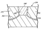
図4に示されるように、成形後、基板254の一部および磁性材料252の一部が除去される。より特定的には、磁性材料252は、前縁249と、後縁248と、1対の対向する側壁262および264とを含むように規定される。なお、後縁248は、図1に示される記録磁極116の後縁148に一致する。
As shown in FIG. 4, after the molding, a part of the
ブロック205において、第3の中間構造268(図5に図示)を形成するために、第1の保護層266が第2の中間構造258上に堆積される。第1の保護層266は、イオンミリングに晒された基板254の部分と接触し、磁性材料252の側壁262および264、ならびにマスク256の、磁性材料252と接触していない部分と接触するように、堆積される。たとえば、第1の保護層266は、原子堆積(atomic deposition)(A
LD)で形成することができ、タンタル(Ta)、ルテニウム(Ru)、銅(Cu)、ダイヤモンド状炭素などの非磁性材料、または、アルミナもしくはさまざまな窒化物もしくは炭化物などの他の類似の材料を含み得る。図2に示される方法では、ステップ203および205は、真空を破壊することなく実行することができる。真空下でこれらのステップを実行することは、湿気および酸素に晒されることなどの環境条件に起因して側壁262および264が損傷を受けることを防ぐ。第1の保護層266が堆積されるとすぐに、磁性材料252が晒されることに関する問題が解消され、真空を破壊することができる。
At
LD) and non-magnetic materials such as tantalum (Ta), ruthenium (Ru), copper (Cu), diamond-like carbon, or other similar materials such as alumina or various nitrides or carbides Can be included. In the method shown in FIG. 2,
ブロック207において、図6に示される第4の中間構造272を形成するために、第3の中間構造268が埋め戻し材料270で埋め戻しされる。たとえば、埋め戻し材料270は、アルミナなどの絶縁材料であり得る。示されるように、埋め戻し材料270は、ブロック204において記載された成形ステップ中にミリングによって取除かれた磁性材料252の側壁262および264を取囲む空間を埋める。また、図6に示されるように、構造272を第1の部分275と第2の部分276とに分割する停止面274が、磁性材料252とマスク256との間に規定される。より特定的には、停止面274は、磁性材料252とマスク256との間の境界面によって規定される。
At
ブロック209において、第5の中間構造278(図7に図示)を形成するために、第4の中間構造272の第1の部分275が停止面274において除去される。第1の部分275を除去することによって、成形された磁性材料252の後縁248を晒すように、第1の保護層266の一部、埋め戻し材料270の一部およびマスク256が除去される。
At
ブロック211において、第6の中間構造282を形成するために、第2の保護層280が第5の中間構造278上に堆積される。特に、第2の保護層280は、埋め戻し材料270、第1の保護層266および成形された磁性材料252の後縁248を被覆するように堆積される。したがって、成形された磁性材料252は、側壁262および264と接触する保護層および後縁248上の保護層によって被覆され、保護される。第1の保護層266と同様に、第2の保護層280は、タンタル(Ta)、ルテニウム(Ru)、銅(Cu)、ダイヤモンド状炭素などの非磁性材料、または、アルミナもしくはさまざまな窒化物もしくは炭化物などの他の類似の材料を含み得る。
In
ブロック213において、(図1に示される間隙または空間120などの)間隙を形成するために、間隙材料284が第6の中間構造282上に堆積される(または、図9に示されるように、第2の保護層280上に堆積される)。シールドまたは前面シールドを形成するために、シールド材料286(図1には特に図示せず)が間隙材料284上に堆積される。間隙材料284およびシールド材料286を追加することによって、第6の中間構造282がトランスデューサ202の少なくとも一部になる。たとえば、間隙材料284はアルミナなどの絶縁材料であり得て、シールド材料286は磁性材料であり得る。前に記載したように、シールド材料286は、後縁248における磁場勾配を大きくし、遷移の質を改善する。
At
図10は、図1のトランスデューサ102などのトランスデューサの製造方法の別の実施例を示すフローチャート300である。特に、フローチャート300は、図1に示される記録磁極116などの記録磁極の製造方法を記載する。フローチャート300は、図11〜図16に示される中間構造と組合せて記載される。
FIG. 10 is a
ブロック301において、図11に示されるような第1の中間構造350が得られる。第1の中間構造350は、基板354上に形成された磁性材料352を含む。図3の磁性材料252と同様に、磁性材料352は、FeCoまたは他のタイプの2.4T鉄コバルトであり得る。基板254と同様に、基板354は、アルミナまたは他のタイプの絶縁材料であり得る。第1の中間構造350は、また、磁性材料352上に形成された第1の保護層366と、第1の保護層366上に堆積されたマスク356とを含む。図5の第1の保護層266と同様に、第1の保護層366は、タンタル(Ta)、ルテニウム(Ru)、銅(Cu)、ダイヤモンド状炭素などの非磁性材料、または、アルミナもしくはさまざまな窒化物もしくは炭化物などの他の類似の材料を含み得る。図3のマスク256と同様に、マスク356は、フォトレジストまたは硬質マスクであり得る。マスク356は、製造すべき記録磁極の幅を規定することに用いられるように構成される。
In
ブロック303において、第2の中間構造358(図12に図示)を形成するために、少なくとも1回の成形作業が第1の中間構造350上で実行される。磁性材料の形状を規定するために、マスク356によって塞がれていない磁性材料352および第1の保護層366の除去を、イオンミリングまたは反応性イオンビームエッチング(RIBE)などの他の技術によって、行なうことができる。図12に示されるように、成形後、基板354の一部、磁性材料352の一部および第1の保護層366の一部が除去される。より特定的には、磁性材料352は、後縁348と、前縁349と、1対の対向する側壁362および364とを含むように規定される。なお、後縁348は、図1に示される記録磁極116の後縁148に一致する。
At
ブロック305において、第3の中間構造368(図13に逗子)を形成するために、大2の保護層380が第2の中間構造358上に堆積される。第2の保護層380は、イオンミリングに晒された基板354の部分と接触し、磁性材料352の側壁362および364ならびに第1の保護材料366の側面ならびにマスク356の部分と接触するように、堆積される。したがって、成形された磁性材料352は、側壁362および364と接触する保護層および後縁348上の保護層によって被覆され、保護される。第1の保護層366と同様に、第2の保護層380は、タンタル(Ta)、ルテニウム(Ru)、銅(Cu)、ダイヤモンド状炭素などの非磁性材料、または、アルミナもしくはさまざまな窒化物もしくは炭化物などの他の類似の材料を含み得る。
At
図10に示される方法では、ステップ303および305は、真空を破壊することなく実行することができる。真空下でこれらのステップを実行することは、湿気および酸素に晒されることなどの環境条件に起因して側壁362および364が損傷を受けることを防ぐ。第1の保護層366および第2の保護層380が堆積されるとすぐに、磁性材料352が晒されることに関する問題が解消され、真空を破壊することができる。
In the method shown in FIG. 10,
ブロック307において、第4の中間構造372(図14に図示)を形成するために、第3の中間構造368が埋め戻し材料370で埋め戻しされる。埋め戻し材料270と同様に、埋め戻し材料370は、アルミナなどの絶縁材料であり得る。示されるように、埋め戻し材料370は、ブロック303において記載された成形ステップ中にミリングによって取除かれ、第2の保護層380でコーティングされた磁性材料352の側壁362および364を取囲む空間を埋める。また、図14に示されるように、構造372を第1の部分375と第2の部分376とに分割する停止面374が、磁性材料352とマスク356との間に規定される。より特定的には、停止面374は、第1の保護層366とマスク356との間の境界面によって規定される。
At
ブロック309において、第5の中間構造378(図15に図示)を形成するために、第4の中間構造372の第1の部分375が停止面374において除去される。第1の部分375を除去することによって、成形された磁性材料352の後縁348上に形成された第1の保護層366を晒すように、第2の保護層380の一部、埋め戻し材料370の一部およびマスク356が除去される。
At
ブロック311において、(図1に示される間隙または空間120などの)間隙を形成するために、間隙材料384が第6の中間構造382上に堆積される(または、図16に示されるように、第2の保護層366および埋め戻し370上に堆積される)。シールドまたは前面シールドを形成するために、シールド材料386(図1には特に図示せず)が間隙材料384上に堆積される。間隙材料384およびシールド材料386を追加することによって、第6の中間構造382がトランスデューサ302の少なくとも一部になる。たとえば、間隙材料384はアルミナなどの絶縁材料であり得て、シールド材料386は磁性材料であり得る。前に記載したように、シールド材料386は、後縁348における磁場勾配を大きくし、遷移の質を改善する。
At
図17は、図1のトランスデューサ102などのトランスデューサの製造方法の別の実施例を示すフローチャート400である。特に、フローチャート400は、図1に示される記録磁極116などの記録磁極の製造方法を記載する。フローチャート400は、図18〜図20に示される中間構造と組合せて記載される。
FIG. 17 is a
ブロック401において、図18に示されるような第1の中間構造450が得られる。第1の中間構造450は、基板454上に形成された磁性材料452を含む。図3の磁性材料252および図11の磁性材料352と同様に、磁性材料452は、FeCoまたは他のタイプの2.4T鉄コバルトであり得る。基板254および基板354と同様に、基板454は、アルミナまたは他のタイプの絶縁材料であり得る。第1の中間構造450は、また、磁性材料452上に堆積されたマスク456を含む。たとえば、マスク456は、フォトレジストまたは硬質マスクであり得る。マスク456は、製造される記録磁極の幅を規定することに用いられるように構成される。一般に、記録磁極の幅は、記憶媒体上のトラックの幅に対応すべきである。
In
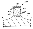
ブロック403において、第2の中間構造458(図19に図示)を形成するために、少なくとも1回の成形作業が第1の中間構造450上で実行される。磁性材料の形状を規定するために、マスク456によって塞がれていない磁性材料452の除去を、イオンミリングまたは反応性イオンビームエッチング(RIBE)などの他の技術によって、第1のエネルギレベルで行なうことができ、第2の中間構造458を形成する。特に、第1の成形作業は、誘導性イオンビームミルによって実行することができる。図19に示されるように、成形後、基板454の一部および磁性材料452の一部が除去される。より特定的には、磁性材料452は、前縁449と、後縁448と、1対の対向する側壁462および464とを含むように規定される。なお、後縁448は、図1に示される記録磁極116の後縁148に一致する。
At
しかしながら、第1の成形作業が磁性材料452上で実行された後、磁性材料452の側面では、制御されない厚みを有する反応ゾーンまたは不感層490の形成が生じる。不感層490の形成は、さまざまな理由によって引き起こされる可能性がある。たとえば、イオンミリング中にデバイスの側壁462および464に打込まれるアルゴンビームは、イオンにより誘発される物理的損傷を引き起こす可能性がある。別の例では、磁性材料452がイオンミリングによって規定された後、磁性材料452は、他の製造プロセスに遷移するための雰囲気に晒される可能性がある。イオンミリング処理されたばかりのデバイスが雰囲気に晒されるために、酸素および水分が容易にデバイスの端縁と反応し得て、不感層490を形成する。さらに別の例では、側壁462および464に対するその後の酸化が、アルミナ硬質マスクまたは他のアルミナ層から生じ得る。
However, after the first molding operation is performed on the
実際、不感層490が磁性材料452上に形成される場合、図20に示されるような第3の中間構造468を形成するために磁性材料452上で第2の成形作業を実行することによって、不感層の厚みを除去または低減することができる。第2の成形作業は、イオンミリングまたはRIBEなどの他の技術によって、第2のエネルギレベルで実行することができる。特に、第2の成形作業は、誘導性イオンビームミルを用いて実行することができる。第2のエネルギレベルは、減少した量または第1のエネルギレベルよりも少ない量のエネルギレベルである。より低いパワーで第2の成形作業を実行することは、第1の成形作業下で形成された損傷層または不感層490と比較して、磁性材料の側壁462および464上の新たな損傷層または不感層491が小さくなることを意味する。また、図20に示されるように、第2の中間構造458上での第2の成形作業は、磁性材料452と基板454との間の境界面に直角(すなわち、磁性材料452の前縁449に直角)の位置に対して第1の角度492で実行される。
Indeed, when the
ブロック405においておよび図21に示されるように、側壁462および464上に保護または封じ込め層466を形成するために、基板454の材料が、イオンビーム打込みを用いて、第2の中間構造458または第3の中間構造468の磁性材料452の側壁462および464上に再堆積される。特に、基板材料を基板454から側壁462および464上に再堆積させるためにイオンビーム打込みを行なうステップは、磁性材料452と基板454との間の境界面に直角(すなわち、磁性材料452の前縁449に直角)の位置において実行される。図21に示されるように、イオンビーム打込みの直角位置によって、基板454のアルミナが基板から解き放たれ、側壁462および464上に堆積する。図20に示される第2の成形作業も図21に示される再堆積作業も、誘導性イオンビームミルを用いて、第2のエネルギレベルで実行することができ、この第2のエネルギレベルは、図19に示される第1の成形作業を実行するためのエネルギレベルよりも低いエネルギレベルである。
In
図19〜図21に示されるすべてのステップが、真空を破壊することなく単一のチャンバ内で実行できることを理解されたい。さらに、図21に示される時点で磁性材料452が依然としてマスク456によって被覆されているので、前縁449に直角の位置において行なわれるイオンビーム打込みを用いた再堆積作業が、製造中のトランスデューサの限界寸法(すなわち、幅)に影響を及ぼさないことを認識されたい。
It should be understood that all steps shown in FIGS. 19-21 can be performed in a single chamber without breaking the vacuum. Furthermore, since the
さまざまな実施例の構造および機能の詳細とともに、さまざまな実施例の多数の特徴および利点について上記の説明の中で記載してきたが、この開示は例示的なものであるに過ぎず、詳細について、特に、添付の特許請求の範囲を表現する用語の幅広い一般的な意味によって示される開示の原理の最大の範囲内で、部品の構造および配置の事項について、変更を行なってもよい。たとえば、特定の素子は、本発明の範囲および精神から逸脱することなく、実質的に同じ機能を維持しながら、トランスデューサのタイプによって異なっていてもよい。また、本明細書に記載される実施例は、製造中に記録磁極を保護することに向けられているが、本発明の教示が、本発明の範囲および精神から逸脱することなく、製造中の他のタイプのトランスデューサの他の構成要素に適用可能であることは、当業者によって理解される。 Although numerous features and advantages of various embodiments have been described in the above description, along with details of the structure and function of the various embodiments, this disclosure is illustrative only, In particular, changes may be made in the structure and arrangement of components within the maximum scope of the disclosed principles as indicated by the broad general meaning of the terms used to describe the appended claims. For example, the particular elements may vary from one transducer type to another while maintaining substantially the same function without departing from the scope and spirit of the present invention. Also, while the embodiments described herein are directed to protecting the recording pole during manufacture, the teachings of the present invention may be used during manufacture without departing from the scope and spirit of the present invention. It will be appreciated by those skilled in the art that it is applicable to other components of other types of transducers.
102 トランスデューサ、148 後縁、149 前縁、252 磁性材料、254 基板、262,264 側壁、266 第1の保護層、270 埋め戻し材料 102 transducer, 148 trailing edge, 149 leading edge, 252 magnetic material, 254 substrate, 262, 264 sidewall, 266 first protective layer, 270 backfill material
Claims (2)
基板上に形成された磁性材料と、前記磁性材料上に堆積されたマスクとを含む第1の中間構造を得るステップと、
第2の中間構造を形成するために、イオンビーム打込みを用いて、第1のエネルギレベルで、前記第1の中間構造上で第1の成形作業を実行するステップとを備え、前記第2の中間構造における成形された磁性材料は、後縁と、前縁と、前記後縁および前記前縁の間に延びる1対の側壁とを含み、前記方法はさらに、
保護層を形成するために、前記第1のエネルギレベルよりも低い第2のエネルギレベルでのイオンビーム打込みを用いて、前記第2の中間構造における前記成形された磁性材料の前記側壁上に、前記側壁と接触して前記基板の材料を再堆積させるステップを備える、方法。 A transducer manufacturing method comprising:
Obtaining a first intermediate structure comprising a magnetic material formed on a substrate and a mask deposited on the magnetic material;
Performing a first forming operation on the first intermediate structure at a first energy level using an ion beam implant to form a second intermediate structure, the second intermediate structure comprising: The shaped magnetic material in the intermediate structure includes a trailing edge, a leading edge, and a pair of sidewalls extending between the trailing edge and the leading edge, the method further comprising:
On the sidewalls of the shaped magnetic material in the second intermediate structure using ion beam implantation at a second energy level lower than the first energy level to form a protective layer, Re-depositing the material of the substrate in contact with the sidewall.
基板上に形成された磁性材料と、前記磁性材料上に堆積されたマスクとを含む第1の中間構造を得るステップを備え、前記構造を第1の部分と第2の部分とに分割する停止面が、前記磁性材料と前記マスクとの間に規定され、前記方法はさらに、
第2の中間構造を形成するために、前記第1の中間構造上で少なくとも1回の成形作業を実行するステップと、
第3の中間構造を形成するために、前記第2の中間構造上に非磁性材料からなる第1の保護層を堆積させるステップと、
第4の中間構造を形成するために、絶縁材料で前記第3の中間構造を埋め戻しするステップと、
第5の中間構造を形成するために、埋め戻しされた絶縁材料の一部、前記マスクの全体および前記第1の保護層の一部を含む前記構造の前記第1の部分を前記停止面において除去するステップとを備える、方法。 A transducer manufacturing method comprising:
Obtaining a first intermediate structure comprising a magnetic material formed on a substrate and a mask deposited on said magnetic material, said stop being divided into a first part and a second part A surface is defined between the magnetic material and the mask, the method further comprising:
Performing at least one molding operation on the first intermediate structure to form a second intermediate structure;
Depositing a first protective layer of a non-magnetic material on the second intermediate structure to form a third intermediate structure;
Backfilling the third intermediate structure with an insulating material to form a fourth intermediate structure;
The first portion of the structure including a portion of the backfilled insulating material, the entire mask and a portion of the first protective layer to form a fifth intermediate structure at the stop surface Removing the method.
Applications Claiming Priority (2)
| Application Number | Priority Date | Filing Date | Title |
|---|---|---|---|
| US12/502,179 | 2009-07-13 | ||
| US12/502,179 US9058823B2 (en) | 2009-07-13 | 2009-07-13 | Protected transducer for dead layer reduction |
Related Parent Applications (1)
| Application Number | Title | Priority Date | Filing Date |
|---|---|---|---|
| JP2010158107A Division JP5675192B2 (en) | 2009-07-13 | 2010-07-12 | Transducer and transducer manufacturing method |
Publications (2)
| Publication Number | Publication Date |
|---|---|
| JP2014238911A JP2014238911A (en) | 2014-12-18 |
| JP5905552B2 true JP5905552B2 (en) | 2016-04-20 |
Family
ID=43427285
Family Applications (2)
| Application Number | Title | Priority Date | Filing Date |
|---|---|---|---|
| JP2010158107A Expired - Fee Related JP5675192B2 (en) | 2009-07-13 | 2010-07-12 | Transducer and transducer manufacturing method |
| JP2014192851A Active JP5905552B2 (en) | 2009-07-13 | 2014-09-22 | Transducer and transducer manufacturing method |
Family Applications Before (1)
| Application Number | Title | Priority Date | Filing Date |
|---|---|---|---|
| JP2010158107A Expired - Fee Related JP5675192B2 (en) | 2009-07-13 | 2010-07-12 | Transducer and transducer manufacturing method |
Country Status (3)
| Country | Link |
|---|---|
| US (1) | US9058823B2 (en) |
| JP (2) | JP5675192B2 (en) |
| CN (1) | CN101996642B (en) |
Families Citing this family (2)
| Publication number | Priority date | Publication date | Assignee | Title |
|---|---|---|---|---|
| US20100108636A1 (en) * | 2008-10-30 | 2010-05-06 | Seagate Technology Llc | Integrated Tool for Fabricating an Electronic Component |
| KR102411080B1 (en) * | 2015-09-02 | 2022-06-21 | 삼성전자주식회사 | Method for forming patterns and method for manufacturing magnetic memory device using the same |
Family Cites Families (26)
| Publication number | Priority date | Publication date | Assignee | Title |
|---|---|---|---|---|
| US5734531A (en) * | 1995-10-31 | 1998-03-31 | Quantum Peripherals Colorado, Inc. | Magneto-resistive read/write head having a combination pole/shield |
| US6264848B1 (en) * | 1998-04-09 | 2001-07-24 | Seagate Technology Llc | Method for providing track position and identification information for data storage devices |
| US6519119B1 (en) * | 1999-11-03 | 2003-02-11 | Seagate Technology, Llc | Structure for current perrpendicular to plane giant magnetoresistive read heads |
| JP2002367112A (en) * | 2001-06-08 | 2002-12-20 | Tdk Corp | Method for manufacturing thin film magnetic head |
| US6687085B2 (en) | 2001-07-17 | 2004-02-03 | Seagate Technology Llc | Perpendicular write head with high magnetization pole material and method of fabricating the write head |
| JP2003298139A (en) | 2002-03-29 | 2003-10-17 | Alps Electric Co Ltd | Magnetic detecting element |
| JP2003332649A (en) | 2002-05-14 | 2003-11-21 | Alps Electric Co Ltd | Magnetic detecting element |
| US6998061B1 (en) | 2002-09-06 | 2006-02-14 | Maxtor Corporation | In-situ exchange biased GMR head for ultra-high density recording with pinning layer-only anneal |
| US7292409B1 (en) | 2004-02-27 | 2007-11-06 | Western Digital (Fremont), Llc | Magnetic head with thin trailing pedestal layer |
| US7367110B2 (en) | 2004-09-27 | 2008-05-06 | Hitachi Global Storage Technologies Netherlands B.V. | Method of fabricating a read head having shaped read sensor-biasing layer junctions using partial milling |
| US7228619B2 (en) | 2004-10-29 | 2007-06-12 | Hitachi Global Storage Technologies Netherlands B.V. | Method of manufacturing a magnetic head with common seed layer for coil and pedestal |
| JP2006134507A (en) * | 2004-11-08 | 2006-05-25 | Tdk Corp | Manufacturing method of magnetic head, magnetic head, head gimbal assembly, head arm assembly, and head stack assembly |
| US7639456B2 (en) | 2005-10-06 | 2009-12-29 | Hitachi Global Storage Technologies Netherlands B.V. | Double mill process for patterning current perpendicular to plane (CPP) magnetoresistive devices to minimize barrier shorting and barrier damage |
| US7446984B2 (en) | 2005-12-14 | 2008-11-04 | Hitachi Global Storage Technologies Netherlands B.V. | Magnetic random access memory (MRAM) having increased reference layer anisotropy through ion beam etch of magnetic layers |
| JP2007184022A (en) | 2006-01-04 | 2007-07-19 | Alps Electric Co Ltd | Manufacturing method of main magnetic pole of perpendicular magnetic recording head |
| US20070183093A1 (en) | 2006-02-07 | 2007-08-09 | Quang Le | Protective layer for CMP assisted lift-off process and method of fabrication |
| JP2007257775A (en) * | 2006-03-24 | 2007-10-04 | Tdk Corp | Method for manufacturing thin-film element having narrow lower layer, and thin-film magnetic head equipped with element |
| US7765677B2 (en) | 2006-04-18 | 2010-08-03 | Hitachi Global Storage Technologies Netherlands B.V. | Method for manufacturing a magnetic write head using a protective layer to prevent write pole consumption |
| US7748103B2 (en) * | 2006-04-24 | 2010-07-06 | Hitachi Global Storage Technologies Netherlands B.V. | Method of manufacturing a perpendicular magnetic recording write head with notched trailing shield |
| US7587811B2 (en) | 2006-04-25 | 2009-09-15 | Hitachi Global Storage Technologies Netherlands B.V. | Method for manufacturing a magnetic write head for perpendicular magnetic data recording |
| JP2008052840A (en) | 2006-08-25 | 2008-03-06 | Hitachi Global Storage Technologies Netherlands Bv | Manufacturing method of magnetic head slider |
| US7578049B2 (en) | 2006-09-21 | 2009-08-25 | Hitachi Global Storage Technologies Netherlands B.V. | Method for constructing a magnetic write pole for a perpendicular magnetic recording head |
| US7715147B2 (en) | 2006-10-27 | 2010-05-11 | Hitachi Global Storage Technologies Netherlands B.V. | Magnetic write head having a shield that extends below the leading edge of the write pole |
| US7993535B2 (en) * | 2007-01-26 | 2011-08-09 | International Business Machines Corporation | Robust self-aligned process for sub-65nm current-perpendicular junction pillars |
| JP2008210481A (en) | 2007-02-27 | 2008-09-11 | Fujitsu Ltd | Manufacturing method of magnetic recording apparatus |
| US20100108636A1 (en) * | 2008-10-30 | 2010-05-06 | Seagate Technology Llc | Integrated Tool for Fabricating an Electronic Component |
-
2009
- 2009-07-13 US US12/502,179 patent/US9058823B2/en active Active
-
2010
- 2010-07-12 JP JP2010158107A patent/JP5675192B2/en not_active Expired - Fee Related
- 2010-07-13 CN CN 201010278034 patent/CN101996642B/en not_active Expired - Fee Related
-
2014
- 2014-09-22 JP JP2014192851A patent/JP5905552B2/en active Active
Also Published As
| Publication number | Publication date |
|---|---|
| CN101996642B (en) | 2013-06-05 |
| US9058823B2 (en) | 2015-06-16 |
| JP2014238911A (en) | 2014-12-18 |
| US20110007422A1 (en) | 2011-01-13 |
| JP5675192B2 (en) | 2015-02-25 |
| CN101996642A (en) | 2011-03-30 |
| JP2011023101A (en) | 2011-02-03 |
Similar Documents
| Publication | Publication Date | Title |
|---|---|---|
| JP4999121B2 (en) | Magnetic head for perpendicular magnetic recording having side shield layer and manufacturing method thereof | |
| US5809636A (en) | Method of making a magnetoresistive thin film magnetic head with specific shapes of leads | |
| US7388732B2 (en) | Perpendicular recording magnetic head with a write shield megnetically coupled to a first pole piece | |
| US6433968B1 (en) | Merged read/write head and method of fabricating same | |
| KR100924695B1 (en) | Vertical magnetic recording head and its manufacturing method | |
| US6999277B2 (en) | Magnetic head having thermally assisted write head with heater element, and protective sacrificial layer | |
| JP2007128581A (en) | Magnetic head and manufacturing method thereof | |
| JP3817223B2 (en) | Thin film magnetic head and manufacturing method thereof | |
| US6665156B2 (en) | Magnetoresistive head, manufacture thereof, and magnetic recording/reproducing apparatus with such magnetic head | |
| JP2002329905A (en) | CPP structure magnetoresistive element and method of manufacturing the same | |
| JP5905552B2 (en) | Transducer and transducer manufacturing method | |
| CN100349210C (en) | Magnetic head and manufacturing method thereof | |
| JP2008192269A (en) | Magnetic read head and manufacturing method thereof | |
| JP2005182897A (en) | Thin film magnetic head and manufacturing method thereof | |
| US10950261B2 (en) | Supermalloy and MU metal side and top shields for magnetic read heads | |
| KR100617282B1 (en) | CPU structure magnetoresistive element | |
| JPH10154312A (en) | Magnetic head and method of manufacturing the same | |
| JP3902183B2 (en) | Magnetic head, manufacturing method thereof, and magnetic recording / reproducing apparatus | |
| US6404588B1 (en) | Thin film magnetic head having magnetic yoke layer connected to magnetic yoke piece of reduced width | |
| JP3639529B2 (en) | Thin film magnetic head and method of manufacturing thin film magnetic head | |
| JPH10283617A (en) | Composite head for perpendicular magnetic recording | |
| JP2009205710A (en) | Perpendicular magnetic recording head and method for manufacturing the same | |
| JP2000215411A (en) | Thin film magnetic head and its manufacture | |
| JP2008140521A (en) | Magnetic head and manufacturing method thereof | |
| JP2007026562A (en) | Thin film magnetic head and manufacturing method thereof |
Legal Events
| Date | Code | Title | Description |
|---|---|---|---|
| A621 | Written request for application examination |
Free format text: JAPANESE INTERMEDIATE CODE: A621 Effective date: 20141014 |
|
| A977 | Report on retrieval |
Free format text: JAPANESE INTERMEDIATE CODE: A971007 Effective date: 20150615 |
|
| A131 | Notification of reasons for refusal |
Free format text: JAPANESE INTERMEDIATE CODE: A131 Effective date: 20150707 |
|
| A601 | Written request for extension of time |
Free format text: JAPANESE INTERMEDIATE CODE: A601 Effective date: 20151006 |
|
| A521 | Written amendment |
Free format text: JAPANESE INTERMEDIATE CODE: A523 Effective date: 20151102 |
|
| TRDD | Decision of grant or rejection written | ||
| A01 | Written decision to grant a patent or to grant a registration (utility model) |
Free format text: JAPANESE INTERMEDIATE CODE: A01 Effective date: 20160216 |
|
| A61 | First payment of annual fees (during grant procedure) |
Free format text: JAPANESE INTERMEDIATE CODE: A61 Effective date: 20160316 |
|
| R150 | Certificate of patent or registration of utility model |
Ref document number: 5905552 Country of ref document: JP Free format text: JAPANESE INTERMEDIATE CODE: R150 |
|
| R250 | Receipt of annual fees |
Free format text: JAPANESE INTERMEDIATE CODE: R250 |
|
| R250 | Receipt of annual fees |
Free format text: JAPANESE INTERMEDIATE CODE: R250 |