JP5851734B2 - Liquid crystal display - Google Patents
Liquid crystal display Download PDFInfo
- Publication number
- JP5851734B2 JP5851734B2 JP2011142754A JP2011142754A JP5851734B2 JP 5851734 B2 JP5851734 B2 JP 5851734B2 JP 2011142754 A JP2011142754 A JP 2011142754A JP 2011142754 A JP2011142754 A JP 2011142754A JP 5851734 B2 JP5851734 B2 JP 5851734B2
- Authority
- JP
- Japan
- Prior art keywords
- transistor
- film
- liquid crystal
- signal
- region
- Prior art date
- Legal status (The legal status is an assumption and is not a legal conclusion. Google has not performed a legal analysis and makes no representation as to the accuracy of the status listed.)
- Expired - Fee Related
Links
Images


Classifications
-
- G—PHYSICS
- G09—EDUCATION; CRYPTOGRAPHY; DISPLAY; ADVERTISING; SEALS
- G09G—ARRANGEMENTS OR CIRCUITS FOR CONTROL OF INDICATING DEVICES USING STATIC MEANS TO PRESENT VARIABLE INFORMATION
- G09G3/00—Control arrangements or circuits, of interest only in connection with visual indicators other than cathode-ray tubes
- G09G3/20—Control arrangements or circuits, of interest only in connection with visual indicators other than cathode-ray tubes for presentation of an assembly of a number of characters, e.g. a page, by composing the assembly by combination of individual elements arranged in a matrix no fixed position being assigned to or needed to be assigned to the individual characters or partial characters
- G09G3/34—Control arrangements or circuits, of interest only in connection with visual indicators other than cathode-ray tubes for presentation of an assembly of a number of characters, e.g. a page, by composing the assembly by combination of individual elements arranged in a matrix no fixed position being assigned to or needed to be assigned to the individual characters or partial characters by control of light from an independent source
- G09G3/36—Control arrangements or circuits, of interest only in connection with visual indicators other than cathode-ray tubes for presentation of an assembly of a number of characters, e.g. a page, by composing the assembly by combination of individual elements arranged in a matrix no fixed position being assigned to or needed to be assigned to the individual characters or partial characters by control of light from an independent source using liquid crystals
- G09G3/3611—Control of matrices with row and column drivers
- G09G3/3674—Details of drivers for scan electrodes
- G09G3/3677—Details of drivers for scan electrodes suitable for active matrices only
-
- G—PHYSICS
- G02—OPTICS
- G02F—OPTICAL DEVICES OR ARRANGEMENTS FOR THE CONTROL OF LIGHT BY MODIFICATION OF THE OPTICAL PROPERTIES OF THE MEDIA OF THE ELEMENTS INVOLVED THEREIN; NON-LINEAR OPTICS; FREQUENCY-CHANGING OF LIGHT; OPTICAL LOGIC ELEMENTS; OPTICAL ANALOGUE/DIGITAL CONVERTERS
- G02F1/00—Devices or arrangements for the control of the intensity, colour, phase, polarisation or direction of light arriving from an independent light source, e.g. switching, gating or modulating; Non-linear optics
- G02F1/01—Devices or arrangements for the control of the intensity, colour, phase, polarisation or direction of light arriving from an independent light source, e.g. switching, gating or modulating; Non-linear optics for the control of the intensity, phase, polarisation or colour
- G02F1/13—Devices or arrangements for the control of the intensity, colour, phase, polarisation or direction of light arriving from an independent light source, e.g. switching, gating or modulating; Non-linear optics for the control of the intensity, phase, polarisation or colour based on liquid crystals, e.g. single liquid crystal display cells
- G02F1/133—Constructional arrangements; Operation of liquid crystal cells; Circuit arrangements
- G02F1/136—Liquid crystal cells structurally associated with a semi-conducting layer or substrate, e.g. cells forming part of an integrated circuit
- G02F1/1362—Active matrix addressed cells
- G02F1/1368—Active matrix addressed cells in which the switching element is a three-electrode device
-
- G—PHYSICS
- G09—EDUCATION; CRYPTOGRAPHY; DISPLAY; ADVERTISING; SEALS
- G09G—ARRANGEMENTS OR CIRCUITS FOR CONTROL OF INDICATING DEVICES USING STATIC MEANS TO PRESENT VARIABLE INFORMATION
- G09G3/00—Control arrangements or circuits, of interest only in connection with visual indicators other than cathode-ray tubes
- G09G3/20—Control arrangements or circuits, of interest only in connection with visual indicators other than cathode-ray tubes for presentation of an assembly of a number of characters, e.g. a page, by composing the assembly by combination of individual elements arranged in a matrix no fixed position being assigned to or needed to be assigned to the individual characters or partial characters
- G09G3/34—Control arrangements or circuits, of interest only in connection with visual indicators other than cathode-ray tubes for presentation of an assembly of a number of characters, e.g. a page, by composing the assembly by combination of individual elements arranged in a matrix no fixed position being assigned to or needed to be assigned to the individual characters or partial characters by control of light from an independent source
- G09G3/36—Control arrangements or circuits, of interest only in connection with visual indicators other than cathode-ray tubes for presentation of an assembly of a number of characters, e.g. a page, by composing the assembly by combination of individual elements arranged in a matrix no fixed position being assigned to or needed to be assigned to the individual characters or partial characters by control of light from an independent source using liquid crystals
- G09G3/3611—Control of matrices with row and column drivers
- G09G3/3685—Details of drivers for data electrodes
- G09G3/3688—Details of drivers for data electrodes suitable for active matrices only
-
- G—PHYSICS
- G09—EDUCATION; CRYPTOGRAPHY; DISPLAY; ADVERTISING; SEALS
- G09G—ARRANGEMENTS OR CIRCUITS FOR CONTROL OF INDICATING DEVICES USING STATIC MEANS TO PRESENT VARIABLE INFORMATION
- G09G2310/00—Command of the display device
- G09G2310/02—Addressing, scanning or driving the display screen or processing steps related thereto
- G09G2310/0235—Field-sequential colour display
-
- G—PHYSICS
- G09—EDUCATION; CRYPTOGRAPHY; DISPLAY; ADVERTISING; SEALS
- G09G—ARRANGEMENTS OR CIRCUITS FOR CONTROL OF INDICATING DEVICES USING STATIC MEANS TO PRESENT VARIABLE INFORMATION
- G09G3/00—Control arrangements or circuits, of interest only in connection with visual indicators other than cathode-ray tubes
- G09G3/20—Control arrangements or circuits, of interest only in connection with visual indicators other than cathode-ray tubes for presentation of an assembly of a number of characters, e.g. a page, by composing the assembly by combination of individual elements arranged in a matrix no fixed position being assigned to or needed to be assigned to the individual characters or partial characters
- G09G3/34—Control arrangements or circuits, of interest only in connection with visual indicators other than cathode-ray tubes for presentation of an assembly of a number of characters, e.g. a page, by composing the assembly by combination of individual elements arranged in a matrix no fixed position being assigned to or needed to be assigned to the individual characters or partial characters by control of light from an independent source
- G09G3/3406—Control of illumination source
- G09G3/3413—Details of control of colour illumination sources
Description
トランジスタを画素に有するアクティブマトリクス型の液晶表示装置に関する。 The present invention relates to an active matrix liquid crystal display device including a transistor in a pixel.
透過型の液晶表示装置の場合、バックライトの消費電力が液晶表示装置全体の消費電力に大きく影響を及ぼすため、パネルの内部における光の損失を如何に低減できるかが消費電力削減の重要なポイントとなる。パネルの内部における光の損失は、層間絶縁膜における光の屈折や、カラーフィルタによる光の吸収などによりもたらされる。特に、カラーフィルタは、色素による光の吸収を利用することで白色光から特定の波長領域の光を取り出すため、原理的に光の損失が大きい。実際にバックライトからの光のエネルギーは、カラーフィルタにより70%以上も吸収される。よって、カラーフィルタは液晶表示装置の低消費電力化を阻む要因の一つといえる。 In the case of a transmissive liquid crystal display device, the power consumption of the backlight greatly affects the power consumption of the entire liquid crystal display device, so how to reduce the light loss inside the panel is an important point for reducing power consumption. It becomes. Light loss inside the panel is caused by light refraction in the interlayer insulating film, light absorption by the color filter, and the like. In particular, since the color filter extracts light in a specific wavelength region from white light by utilizing light absorption by the pigment, in principle, light loss is large. Actually, 70% or more of the energy of light from the backlight is absorbed by the color filter. Therefore, it can be said that the color filter is one of the factors hindering the low power consumption of the liquid crystal display device.
カラーフィルタによる光の損失の問題を回避するためには、フィールドシーケンシャル駆動(FS駆動)が有効である。FS駆動は、異なる色相の光を発する複数の光源を順次点灯させることでカラーの画像を表示する駆動方法である。FS駆動ではカラーフィルタを用いる必要がないため、パネルの内部における光の損失を低減することができ、パネルの透過率を高めることができる。よって、バックライトからの光の利用効率を高めることができ、液晶表示装置全体の消費電力を低減させることができる。また、FS駆動では、1つの画素で各色に対応する画像の表示を行うことができるため、高精細な画像の表示を行うことができる。 In order to avoid the problem of light loss due to the color filter, field sequential driving (FS driving) is effective. The FS driving is a driving method for displaying a color image by sequentially lighting a plurality of light sources that emit light of different hues. Since it is not necessary to use a color filter in FS driving, light loss inside the panel can be reduced, and the transmittance of the panel can be increased. Therefore, the utilization efficiency of the light from the backlight can be increased, and the power consumption of the entire liquid crystal display device can be reduced. Further, in the FS driving, since an image corresponding to each color can be displayed with one pixel, a high-definition image can be displayed.
下記特許文献1には、通常はフィールドシーケンシャル方式でのカラー画像の表示を行い、文字などの画像のときにはモノカラー表示に切り換える液晶表示装置について開示されている。
しかし、FS駆動では、各色の画像が合成されずに個別に視認される、カラーブレイクと呼ばれる現象が起こりやすい。特に、カラーブレイクは動画を表示する際に顕著に起こりやすい。 However, in FS driving, a phenomenon called color break, in which images of the respective colors are individually viewed without being synthesized, is likely to occur. In particular, a color break is likely to occur when displaying a moving image.
また、上述したように、フィールドシーケンシャル駆動を用いる場合、カラーフィルタを用いる場合に比べて、液晶表示装置の消費電力を低減させることができる。しかし、携帯用電子機器の普及に伴い液晶表示装置への低消費電力化の要求は厳しさを増しており、更なる消費電力の低減が求められている。 Further, as described above, when field sequential driving is used, the power consumption of the liquid crystal display device can be reduced as compared with the case where a color filter is used. However, with the widespread use of portable electronic devices, the demand for lower power consumption in liquid crystal display devices has become stricter, and further reduction in power consumption is required.
上述の課題に鑑み、本発明は、画質の低下を防ぐことができる液晶表示装置及びその駆動方法の提案を課題の一つとする。或いは、本発明は、消費電力の低減を実現することができる液晶表示装置及びその駆動方法の提案を課題の一つとする。 In view of the above problems, an object of the present invention is to propose a liquid crystal display device and a driving method thereof that can prevent deterioration in image quality. Alternatively, an object of the present invention is to propose a liquid crystal display device that can reduce power consumption and a driving method thereof.
本発明の一態様に係る液晶表示装置は、バックライトが、異なる色相の光を発する複数の光源を有する。そして、フルカラー画像の表示を行う場合と、モノカラー画像の表示を行う場合とで、光源の駆動方法を切り換える。 In the liquid crystal display device according to one embodiment of the present invention, the backlight includes a plurality of light sources that emit light of different hues. Then, the driving method of the light source is switched between when a full color image is displayed and when a monocolor image is displayed.
フルカラー画像の表示を行う場合は、画素部を複数の領域に分割し、領域ごとに上記光源の点灯を制御する。具体的に、本発明の一態様では、画素部が第1の領域及び第2の領域を少なくとも有し、前記第1の領域に、異なる色相を有する複数の光が、第1の輪番に従い順次供給されると共に、前記第2の領域にも異なる色相を有する前記複数の光が、前記第1の輪番とは異なる第2の輪番に従い、順次供給される。 When displaying a full-color image, the pixel portion is divided into a plurality of regions, and lighting of the light source is controlled for each region. Specifically, in one embodiment of the present invention, the pixel portion includes at least a first region and a second region, and a plurality of lights having different hues are sequentially applied to the first region according to a first rotation number. The plurality of lights that are supplied and also have different hues in the second region are sequentially supplied according to a second rotation number different from the first rotation number.
モノカラー画像の表示を行う場合は、画素部全体、或いは領域ごとに、異なる色相を有する複数の光の少なくとも一つを連続して供給する。 In the case of displaying a monochromatic image, at least one of a plurality of lights having different hues is continuously supplied to the entire pixel portion or each region.
さらに、本発明の一態様では、上記モノカラー画像が静止画である場合に、モノカラー画像が動画である場合よりも、その駆動周波数を低くする。そして、本発明の一態様では、駆動周波数を低くするために、液晶表示装置の画素部に、液晶素子と、当該液晶素子に与えられる電圧の保持を制御するための、オフ電流が極めて小さい絶縁ゲート電界効果型トランジスタ(以下、単にトランジスタとする)とを設ける。オフ電流の極めて小さいトランジスタを用いることで、液晶素子に与えられる電圧が保持される期間を長くすることができる。そのため、静止画のように、連続する幾つかのフレーム期間に渡って、画素部に同じ画像情報を有する画像信号が書き込まれる場合などは、駆動周波数を低くしても、言い換えると一定期間内における画像信号の書き込み回数を少なくしても、画像の表示を維持することができる。 Furthermore, in one embodiment of the present invention, when the monocolor image is a still image, the driving frequency is set lower than when the monocolor image is a moving image. In one embodiment of the present invention, in order to reduce the driving frequency, the pixel portion of the liquid crystal display device is provided with an insulating film with extremely low off-state current for controlling the liquid crystal element and holding of the voltage applied to the liquid crystal element. A gate field effect transistor (hereinafter simply referred to as a transistor) is provided. By using a transistor with extremely low off-state current, a period during which a voltage applied to the liquid crystal element is held can be extended. Therefore, when an image signal having the same image information is written in the pixel portion over several consecutive frame periods like a still image, even if the drive frequency is lowered, in other words, within a certain period. Even if the number of times of writing the image signal is reduced, the display of the image can be maintained.
上記トランジスタは、シリコン半導体よりもバンドギャップが広く、真性キャリア密度がシリコン半導体よりも低い半導体材料を、チャネル形成領域に含むことを特徴とする。上述したような特性を有する半導体材料をチャネル形成領域に含むことで、オフ電流が極めて低いトランジスタを実現することができる。このような半導体材料としては、例えば、シリコンの約3倍程度の大きなバンドギャップを有する、酸化物半導体が挙げられる。上記構成を有するトランジスタを、液晶素子に与えられる電圧を保持するためのスイッチング素子として用いることで、通常のシリコンやゲルマニウムなどの半導体材料で形成されたトランジスタを用いた場合に比べて、液晶素子からの電荷のリークを防ぐことができる。 The transistor includes a channel formation region containing a semiconductor material having a wider band gap than a silicon semiconductor and a lower intrinsic carrier density than a silicon semiconductor. By including the semiconductor material having the above characteristics in the channel formation region, a transistor with extremely low off-state current can be realized. As such a semiconductor material, for example, an oxide semiconductor having a large band gap about three times that of silicon can be given. By using the transistor having the above structure as a switching element for holding a voltage applied to the liquid crystal element, the liquid crystal element can be compared with a case where a transistor formed of a semiconductor material such as normal silicon or germanium is used. It is possible to prevent the leakage of charges.
具体的に、本発明の一態様に係る液晶表示装置は、画素部、及び、前記画素部への画像信号の入力を制御する駆動回路が設けられたパネルと、前記画素部に色相の異なる光を供給する複数の光源とを有する。前記画素部は、入力される画像信号の電圧に従って透過率が制御される液晶素子と、前記電圧の保持を制御するトランジスタとを有する。そして、前記トランジスタは、そのチャネル形成領域に、例えば酸化物半導体などの、バンドギャップがシリコン半導体よりも広く、真性キャリア密度がシリコン半導体よりも低い半導体材料を含んでいる。 Specifically, a liquid crystal display device according to one embodiment of the present invention includes a panel provided with a pixel portion and a driver circuit that controls input of an image signal to the pixel portion, and light having a different hue in the pixel portion. A plurality of light sources. The pixel portion includes a liquid crystal element whose transmittance is controlled according to a voltage of an input image signal, and a transistor that controls the holding of the voltage. The transistor includes a semiconductor material having a band gap wider than that of the silicon semiconductor and lower intrinsic carrier density than that of the silicon semiconductor, such as an oxide semiconductor, in the channel formation region.
また、具体的に、本発明の一態様に係る液晶表示装置の駆動方法では、フルカラー画像の表示を行う場合、画素部が第1の領域及び第2の領域を少なくとも有し、前記第1の領域に、異なる色相を有する複数の光が、第1の輪番に従い順次供給されると共に、前記第2の領域にも異なる色相を有する前記複数の光が、前記第1の輪番とは異なる第2の輪番に従い、順次供給される。モノカラー画像の表示を行う場合、画素部全体、或いは領域ごとに、単一の色相を有する光を連続して供給する。そして、画像信号が第1のモノカラー画像の情報を含む場合と、画像信号が第2のモノカラー画像の情報を含む場合とで、一定期間内における前記画像信号の書き込み回数を切り換える。 Specifically, in the driving method of the liquid crystal display device according to one embodiment of the present invention, when a full-color image is displayed, the pixel portion includes at least a first region and a second region, A plurality of lights having different hues are sequentially supplied to the area in accordance with a first rotation number, and the plurality of lights having different hues in the second area are also different from the first rotation number. Are sequentially supplied according to In the case of displaying a monochromatic image, light having a single hue is continuously supplied to the entire pixel portion or each region. Then, the number of times of writing the image signal within a predetermined period is switched between when the image signal includes information of the first monocolor image and when the image signal includes information of the second monocolor image.
なお、電子供与体(ドナー)となる水分または水素などの不純物が低減され、なおかつ酸素の添加により酸素欠損が低減されることで高純度化された酸化物半導体(purified OS)は、i型(真性半導体)又はi型に限りなく近い。そのため、上記酸化物半導体を用いたトランジスタは、オフ電流が著しく低いという特性を有する。具体的に、高純度化された酸化物半導体は、二次イオン質量分析法(SIMS:Secondary Ion Mass Spectrometry)による水素濃度の測定値が、5×10¹⁹/cm3以下、好ましくは5×1018/cm3以下、より好ましくは5×1017/cm3以下、さらに好ましくは1×1016/cm3以下とする。また、ホール効果測定により測定できる酸化物半導体膜のキャリア密度は、1×1014/cm3未満、好ましくは1×1012/cm3未満、さらに好ましくは1×1011/cm3未満とする。また、酸化物半導体のバンドギャップは、2eV以上、好ましくは2.5eV以上、より好ましくは3eV以上である。水分または水素などの不純物濃度が十分に低減され、なおかつ酸素の添加により酸素欠損が低減されることで高純度化された酸化物半導体膜を用いることにより、トランジスタのオフ電流を下げることができる。 Note that an oxide semiconductor (purified OS) that is highly purified by reduction of impurities such as moisture or hydrogen which serves as an electron donor (donor) and oxygen vacancies by addition of oxygen is an i-type ( Intrinsic semiconductor) or i type. Therefore, a transistor including the above oxide semiconductor has a characteristic of extremely low off-state current. Specifically, a highly purified oxide semiconductor has a hydrogen concentration measured by secondary ion mass spectrometry (SIMS) of 5 × 10 19 / cm 3 or less, preferably 5 × 10. 18 / cm 3 or less, more preferably 5 × 10 17 / cm 3 or less, and even more preferably 1 × 10 16 / cm 3 or less. The carrier density of the oxide semiconductor film that can be measured by Hall effect measurement is less than 1 × 10 14 / cm 3 , preferably less than 1 × 10 12 / cm 3 , and more preferably less than 1 × 10 11 / cm 3 . . The band gap of the oxide semiconductor is 2 eV or more, preferably 2.5 eV or more, more preferably 3 eV or more. By using an oxide semiconductor film that is highly purified by the concentration of impurities such as moisture or hydrogen being sufficiently reduced and oxygen vacancies are reduced by the addition of oxygen, the off-state current of the transistor can be reduced.
ここで、酸化物半導体膜中の、水素濃度の分析について触れておく。酸化物半導体膜中及び導電膜中の水素濃度測定は、SIMSで行う。SIMSは、その原理上、試料表面近傍や、材質が異なる膜との積層界面近傍のデータを正確に得ることが困難であることが知られている。そこで、膜中における水素濃度の厚さ方向の分布をSIMSで分析する場合、対象となる膜が存在する範囲において、値に極端な変動が無く、ほぼ一定の値が得られる領域における平均値を、水素濃度として採用する。また、測定の対象となる膜の厚さが小さい場合、隣接する膜内の水素濃度の影響を受けて、ほぼ一定の値が得られる領域を見いだせない場合がある。この場合、当該膜が存在する領域における、水素濃度の極大値または極小値を、当該膜中の水素濃度として採用する。さらに、当該膜が存在する領域において、極大値を有する山型のピーク、極小値を有する谷型のピークが存在しない場合、変曲点の値を水素濃度として採用する。 Here, the analysis of the hydrogen concentration in the oxide semiconductor film is mentioned. The hydrogen concentration in the oxide semiconductor film and the conductive film is measured by SIMS. In SIMS, it is known that it is difficult to accurately obtain data in the vicinity of the sample surface and in the vicinity of the laminated interface with films of different materials. Therefore, when analyzing the distribution in the thickness direction of the hydrogen concentration in the film by SIMS, the average value in a region where there is no extreme variation in the value and an almost constant value is obtained in the range where the target film exists. Adopted as hydrogen concentration. Further, when the thickness of the film to be measured is small, there may be a case where an area where a substantially constant value is obtained cannot be found due to the influence of the hydrogen concentration in the adjacent film. In this case, the maximum value or the minimum value of the hydrogen concentration in the region where the film is present is adopted as the hydrogen concentration in the film. Further, in the region where the film is present, when there is no peak having a maximum value and no valley peak having a minimum value, the value of the inflection point is adopted as the hydrogen concentration.
具体的に、高純度化された酸化物半導体膜を活性層として用いたトランジスタのオフ電流が低いことは、いろいろな実験により証明できる。例えば、チャネル幅が1×106μmでチャネル長が10μmの素子であっても、ソース電極とドレイン電極間の電圧(ドレイン電圧)が1Vから10Vの範囲において、オフ電流(ゲート電極とソース電極間の電圧を0V以下としたときのドレイン電流)が、半導体パラメータアナライザの測定限界以下、すなわち1×10−13A以下という特性を得ることができる。この場合、オフ電流をトランジスタのチャネル幅で除した数値に相当するオフ電流密度は、100zA/μm以下であることが分かる。また、容量素子とトランジスタとを接続して、容量素子に流入または容量素子から流出する電荷を当該トランジスタで制御する回路を用いて、オフ電流密度の測定を行った。当該測定では、上記トランジスタに高純度化された酸化物半導体膜をチャネル形成領域に用い、容量素子の単位時間あたりの電荷量の推移から当該トランジスタのオフ電流密度を測定した。その結果、トランジスタのソース電極とドレイン電極間の電圧が3Vの場合に、数十yA/μmという、さらに低いオフ電流密度が得られることが分かった。したがって、本発明の一態様に係る半導体装置では、高純度化された酸化物半導体膜を活性層として用いたトランジスタのオフ電流密度を、ソース電極とドレイン電極間の電圧によっては、100yA/μm以下、好ましくは10yA/μm以下、更に好ましくは1yA/μm以下にすることができる。従って、高純度化された酸化物半導体膜を活性層として用いたトランジスタは、オフ電流が、結晶性を有するシリコンを用いたトランジスタに比べて著しく低い。 Specifically, it can be proved by various experiments that the off-state current of a transistor using a highly purified oxide semiconductor film as an active layer is low. For example, even in an element having a channel width of 1 × 10 6 μm and a channel length of 10 μm, when the voltage between the source electrode and the drain electrode (drain voltage) is in the range of 1 V to 10 V, the off-current (gate electrode and source electrode) The drain current when the voltage between them is 0 V or less) can be obtained below the measurement limit of the semiconductor parameter analyzer, that is, 1 × 10 −13 A or less. In this case, it can be seen that the off-current density corresponding to a value obtained by dividing the off-current by the channel width of the transistor is 100 zA / μm or less. Further, off-state current density was measured using a circuit in which a capacitor and a transistor are connected and charge flowing into or out of the capacitor is controlled by the transistor. In this measurement, a highly purified oxide semiconductor film of the transistor was used for a channel formation region, and the off-state current density of the transistor was measured from the change in charge amount per unit time of the capacitor. As a result, it was found that when the voltage between the source electrode and the drain electrode of the transistor is 3 V, an even lower off-current density of several tens of yA / μm can be obtained. Therefore, in the semiconductor device according to one embodiment of the present invention, the off-state current density of the transistor using the highly purified oxide semiconductor film as an active layer is 100 yA / μm or less depending on the voltage between the source electrode and the drain electrode. , Preferably 10 yA / μm or less, more preferably 1 yA / μm or less. Therefore, a transistor using a highly purified oxide semiconductor film as an active layer has a significantly lower off-state current than a transistor using crystalline silicon.
なお、酸化物半導体として、酸化インジウム、酸化スズ、酸化亜鉛、二元系金属の酸化物であるIn−Zn系酸化物、Sn−Zn系酸化物、Al−Zn系酸化物、Zn−Mg系酸化物、Sn−Mg系酸化物、In−Mg系酸化物、In−Ga系酸化物、三元系金属の酸化物であるIn−Ga−Zn系酸化物(IGZOとも表記する)、In−Al−Zn系酸化物、In−Sn−Zn系酸化物、Sn−Ga−Zn系酸化物、Al−Ga−Zn系酸化物、Sn−Al−Zn系酸化物、In−Hf−Zn系酸化物、In−La−Zn系酸化物、In−Ce−Zn系酸化物、In−Pr−Zn系酸化物、In−Nd−Zn系酸化物、In−Sm−Zn系酸化物、In−Eu−Zn系酸化物、In−Gd−Zn系酸化物、In−Tb−Zn系酸化物、In−Dy−Zn系酸化物、In−Ho−Zn系酸化物、In−Er−Zn系酸化物、In−Tm−Zn系酸化物、In−Yb−Zn系酸化物、In−Lu−Zn系酸化物、四元系金属の酸化物であるIn−Sn−Ga−Zn系酸化物、In−Hf−Ga−Zn系酸化物、In−Al−Ga−Zn系酸化物、In−Sn−Al−Zn系酸化物、In−Sn−Hf−Zn系酸化物、In−Hf−Al−Zn系酸化物を用いることができる。 Note that as oxide semiconductors, indium oxide, tin oxide, zinc oxide, binary metal oxides such as In—Zn oxides, Sn—Zn oxides, Al—Zn oxides, Zn—Mg oxides are used. Oxides, Sn—Mg oxides, In—Mg oxides, In—Ga oxides, In—Ga—Zn oxides (also referred to as IGZO) which are oxides of ternary metals, In— Al-Zn oxide, In-Sn-Zn oxide, Sn-Ga-Zn oxide, Al-Ga-Zn oxide, Sn-Al-Zn oxide, In-Hf-Zn oxide In-La-Zn-based oxide, In-Ce-Zn-based oxide, In-Pr-Zn-based oxide, In-Nd-Zn-based oxide, In-Sm-Zn-based oxide, In-Eu -Zn oxide, In-Gd-Zn oxide, In-Tb-Zn oxide, I -Dy-Zn oxide, In-Ho-Zn oxide, In-Er-Zn oxide, In-Tm-Zn oxide, In-Yb-Zn oxide, In-Lu-Zn oxide Oxides, In-Sn-Ga-Zn-based oxides that are quaternary metal oxides, In-Hf-Ga-Zn-based oxides, In-Al-Ga-Zn-based oxides, In-Sn-Al A —Zn-based oxide, an In—Sn—Hf—Zn-based oxide, or an In—Hf—Al—Zn-based oxide can be used.
なお、例えば、In−Ga−Zn系酸化物とは、InとGaとZnを有する酸化物という意味であり、InとGaとZnの比率は問わない。また、InとGaとZn以外の金属元素が入っていてもよい。また、酸化物半導体として、InMO3(ZnO)m(m>0、且つ、mは整数でなくてもよい)で表記される材料を用いてもよい。なお、Mは、Ga、Fe、Mn及びCoから選ばれた一の金属元素または複数の金属元素を示す。また、酸化物半導体として、In2SnO5(ZnO)n(n>0、且つ、nは整数)で表記される材料を用いてもよい。 Note that, for example, an In—Ga—Zn-based oxide means an oxide containing In, Ga, and Zn, and there is no limitation on the ratio of In, Ga, and Zn. Moreover, metal elements other than In, Ga, and Zn may be contained. Alternatively, a material represented by InMO 3 (ZnO) m (m> 0 is satisfied, and m may not be an integer) may be used as the oxide semiconductor. Note that M represents one metal element or a plurality of metal elements selected from Ga, Fe, Mn, and Co. Alternatively, a material represented by In 2 SnO 5 (ZnO) n (n> 0 is satisfied, and n is an integer) may be used as the oxide semiconductor.
本発明の一態様に係る液晶表示装置は、画素部を複数の領域に分割し、領域ごとに異なる色相の光を順次供給することで、カラー画像の表示を行う。よって、特定の時刻に着目すると、隣接する領域に供給される光の色相を、互いに異ならせることができる。よって、各色の画像が合成されずに個別に視認されるのを防ぐことができ、動画の表示を行う際に起きやすかったカラーブレイクの発生を防ぐことができる。 In a liquid crystal display device according to one embodiment of the present invention, a pixel portion is divided into a plurality of regions, and light of a different hue is sequentially supplied to each region to display a color image. Therefore, when paying attention to a specific time, the hue of light supplied to adjacent regions can be made different from each other. Therefore, it is possible to prevent the images of the respective colors from being individually viewed without being combined, and it is possible to prevent the occurrence of a color break that easily occurs when displaying a moving image.
なお、異なる色相を有する複数の光源を用いてカラー画像の表示を行う場合、単色の光源とカラーフィルタを組み合わせる場合とは異なり、上記複数の光源を順次切り換えて発光させる必要がある。そして、上記光源の切り換えが行われる周波数は、単色の光源を用いた場合のフレーム周波数よりも高い値に設定する必要がある。例えば、単色の光源を用いた場合のフレーム周波数を60Hzとすると、赤、緑、青の各色に対応する光源を用いてFS駆動を行う場合、光源の切り替えを行う周波数は、3倍の180Hzとなる。よって、駆動回路も上記光源の周波数に合わせて動作させるので、非常に高い周波数で動作を行うことになる。従って、駆動回路における消費電力が、単色の光源とカラーフィルタを組み合わせる場合に比べて高くなりやすい。 Note that when a color image is displayed using a plurality of light sources having different hues, it is necessary to sequentially switch the plurality of light sources to emit light, unlike when combining a single color light source and a color filter. The frequency at which the light source is switched needs to be set to a value higher than the frame frequency when a monochromatic light source is used. For example, assuming that the frame frequency when a monochromatic light source is used is 60 Hz, when FS driving is performed using light sources corresponding to red, green, and blue colors, the frequency for switching the light source is three times 180 Hz. Become. Therefore, since the drive circuit is also operated in accordance with the frequency of the light source, the operation is performed at a very high frequency. Therefore, the power consumption in the drive circuit tends to be higher than when a monochromatic light source and a color filter are combined.
しかし、本発明の一態様では、オフ電流の極めて小さいトランジスタを用いることで、液晶素子に与えられる電圧が保持される期間を長くすることができる。そのため、静止画を表示する際の駆動周波数を、動画を表示する際の駆動周波数よりも低くすることができる。よって、消費電力を低減することができる液晶表示装置を実現することができる。 However, in one embodiment of the present invention, the period in which the voltage applied to the liquid crystal element is held can be extended by using a transistor with extremely low off-state current. Therefore, the driving frequency when displaying a still image can be made lower than the driving frequency when displaying a moving image. Thus, a liquid crystal display device that can reduce power consumption can be realized.
以下では、本発明の実施の形態について図面を用いて詳細に説明する。ただし、本発明は以下の説明に限定されず、本発明の趣旨及びその範囲から逸脱することなくその形態及び詳細を様々に変更し得ることは、当業者であれば容易に理解される。したがって、本発明は、以下に示す実施の形態の記載内容に限定して解釈されるものではない。 Hereinafter, embodiments of the present invention will be described in detail with reference to the drawings. However, the present invention is not limited to the following description, and it will be easily understood by those skilled in the art that modes and details can be variously changed without departing from the spirit and scope of the present invention. Therefore, the present invention should not be construed as being limited to the description of the embodiments below.
(実施の形態1)
<液晶表示装置の構成例>
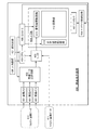
図1に示すように、本実施の形態の液晶表示装置400は、複数の画像メモリ401と、画像データ選択回路402と、セレクタ403と、CPU404と、コントローラ405と、パネル406と、バックライト407と、バックライト制御回路408とを有する。
(Embodiment 1)
<Configuration example of liquid crystal display device>
As shown in FIG. 1, the liquid crystal display device 400 of this embodiment includes a plurality of image memories 401, an image
複数の画像メモリ401には、液晶表示装置400に入力された、フルカラー画像に対応する画像データ(フルカラー画像データ410)が記憶される。上記フルカラー画像データ410には、複数の色相にそれぞれ対応する画像データが含まれている。複数の各画像メモリ401には、各色相に対応する画像データがそれぞれ記憶されている。
In the plurality of image memories 401, image data (full color image data 410) corresponding to the full color image input to the liquid crystal display device 400 is stored. The full
画像メモリ401は、例えばDRAM(Dynamic Random Access Memory)、SRAM(Static Random Access Memory)等の記憶回路を用いることができる。 As the image memory 401, for example, a storage circuit such as a DRAM (Dynamic Random Access Memory) or SRAM (Static Random Access Memory) can be used.
画像データ選択回路402は、コントローラ405からの命令に従って複数の画像メモリ401に記憶されている、各色相に対応するフルカラー画像データを読み出し、セレクタ403に送る。
The image
また、液晶表示装置400には、モノカラー画像に対応する画像データ(モノカラー画像データ411)も入力される。入力されたモノカラー画像データ411は、セレクタ403に入力される。
The liquid crystal display device 400 also receives image data corresponding to a monochromatic image (monochromatic image data 411). The input mono
なお、異なる色相の色を複数用い、各色の階調により表示される画像をフルカラー画像とする。また、単一の色相の色を用い、その色の階調により表示される画像をモノカラー画像とする。 Note that a plurality of colors of different hues are used, and an image displayed with the gradation of each color is a full-color image. Also, a single hue color is used, and an image displayed with the gradation of the color is a monocolor image.
また、本実施の形態では、モノカラー画像データ411が直接セレクタ403に入力される構成を示しているが、本発明はこの構成に限定されない。フルカラー画像データ410と同様に、モノカラー画像データ411も、画像メモリ401において一旦記憶し、画像データ選択回路402において読み出すようにしても良い。この場合、セレクタ403が画像データ選択回路402に含まれる構成となる。
In this embodiment, the mono
また、モノカラー画像データ411は、フルカラー画像データ410を液晶表示装置400において合成することで、作製されていても良い。
The
CPU404は、フルカラー画像の表示を行う場合と、モノカラー画像の表示を行う場合とで、セレクタ403とコントローラ405の動作が切り替わるように制御する。
The
具体的に、フルカラー画像の表示を行う場合、セレクタ403は、CPU404からの命令に従って、入力されたフルカラー画像データ410を選択し、パネル406に供給する。また、コントローラ405は、CPU404からの命令に従って、フルカラー画像データ410に同期した駆動信号またはフルカラー画像の表示を行う際に用いられる電源電位を、パネル406に供給する。
Specifically, when displaying a full-color image, the
或いは、モノカラー画像の表示を行う場合、セレクタ403は、CPU404からの命令に従って、入力されたモノカラー画像データ411を選択し、パネル406に供給する。また、コントローラ405は、CPU404からの命令に従って、モノカラー画像データ411に同期した駆動信号またはモノカラー画像の表示を行う際に用いられる電源電位を、パネル406に供給する。
Alternatively, when displaying a monocolor image, the
パネル406は、各画素に液晶素子を有する画素部412と、信号線駆動回路413、走査線駆動回路414などの駆動回路とを有する。セレクタ403からのフルカラー画像データ410またはモノカラー画像データ411は、信号線駆動回路413に与えられる。また、コントローラ405からの駆動信号または電源電位は、信号線駆動回路413または走査線駆動回路414に与えられる。
The panel 406 includes a pixel portion 412 having a liquid crystal element in each pixel and driving circuits such as a signal line driver circuit 413 and a scanning
なお、駆動信号には、信号線駆動回路413の動作を制御する信号線駆動回路用スタートパルス信号(SSP)、信号線駆動回路用クロック信号(SCK)、走査線駆動回路414の動作を制御する走査線駆動回路用スタートパルス信号(GSP)、走査線駆動回路用クロック信号(GCK)などが含まれる。
Note that the drive signal controls a signal line driver circuit start pulse signal (SSP) for controlling the operation of the signal line driver circuit 413, a signal line driver circuit clock signal (SCK), and an operation of the scanning
バックライト407には、色相の異なる光を発する複数の光源が配置されている。コントローラ405は、バックライト制御回路408を介してバックライト407が有する光源の駆動を制御する。 The backlight 407 is provided with a plurality of light sources that emit light having different hues. The controller 405 controls driving of the light source included in the backlight 407 via the backlight control circuit 408.
なお、フルカラー画像の表示とモノカラー画像の表示の切り替えは、人為的に行うことができる。この場合、入力装置420を液晶表示装置400に設け、入力装置420からの信号に従って、CPU404が上記切り替えを制御するようにすれば良い。
Note that switching between the display of a full-color image and the display of a mono-color image can be performed artificially. In this case, the input device 420 may be provided in the liquid crystal display device 400, and the
また、実施の形態で例示される液晶表示装置400は、測光回路421を有していても良い。測光回路421は当該液晶表示装置400が使用されている環境の明るさを測定する回路である。そして、測光回路421において検知された明るさに従って、CPU404がフルカラー画像の表示とモノカラー画像の表示の切り替えを制御しても良い。
In addition, the liquid crystal display device 400 exemplified in the embodiment may include a photometric circuit 421. The photometric circuit 421 is a circuit that measures the brightness of the environment where the liquid crystal display device 400 is used. Then, the
例えば、本実施の形態で例示される液晶表示装置400を薄暗い環境で利用する場合、測光回路421からの信号に従って、CPU404がフルカラー画像の表示を選択し、明るい環境で利用する場合、測光回路421からの信号に従って、CPU404がモノカラー画像の表示を選択しても良い。なお、測光回路421にあらかじめ閾値を設定し、使用環境の明るさが閾値を下回ると、バックライト407が点灯するように設定してもよい。
For example, when the liquid crystal display device 400 exemplified in this embodiment is used in a dim environment, the
<パネルの構成例>
次いで、本発明の一態様に係る液晶表示装置の、パネルの具体的な構成について、一例を挙げて説明する。
<Example of panel configuration>
Next, a specific structure of the panel of the liquid crystal display device according to one embodiment of the present invention is described with an example.
図2(A)は、液晶表示装置の構成例を示す図である。図2(A)に示す液晶表示装置は、画素部10と、走査線駆動回路11と、信号線駆動回路12とを有する。本発明の一態様では、画素部10が複数の領域に分割されている。具体的に、図2(A)では、画素部10が、3つの領域(領域101〜領域103)に分割されている場合を例示している。そして、各領域は、マトリクス状に配設された複数の画素15を有する。
FIG. 2A illustrates a configuration example of a liquid crystal display device. The liquid crystal display device illustrated in FIG. 2A includes a
また、画素部10には、走査線駆動回路11によって電位が制御されるm本の走査線GLと、信号線駆動回路12によって電位が制御されるn本の信号線SLとが設けられている。そして、m本の走査線GLは、画素部10が有する領域の数に合わせて、複数のグループに分割されている。例えば、図2(A)の場合、画素部10が3つの領域に分割されているので、m本の走査線GLも3つのグループに分割されている。そして、各グループに属する走査線GLは、当該グループに対応する領域が有する複数の画素15に、接続されている。具体的に、各走査線GLは、各領域においてマトリクス状に配設された複数の画素15のうち、いずれかの行に配設されたn個の画素15に接続される。
The
また、各信号線SLは、上記領域に係わらず、画素部10においてm行n列に配設された複数の画素15のうち、いずれかの列に配設されたm個の画素15に接続される。
In addition, each signal line SL is connected to m
なお、本明細書において接続とは電気的な接続を意味しており、電流、電圧または電位が、供給可能、或いは伝送可能な状態に相当する。従って、接続している状態とは、直接接続している状態を必ずしも指すわけではなく、電流、電圧または電位が、供給可能、或いは伝送可能であるように、配線、抵抗、ダイオード、トランジスタなどの回路素子を介して間接的に接続している状態も、その範疇に含む。 Note that in this specification, connection means electrical connection and corresponds to a state where current, voltage, or a potential can be supplied or transmitted. Therefore, the connected state does not necessarily indicate a directly connected state, and a wiring, a resistor, a diode, a transistor, or the like is provided so that current, voltage, or potential can be supplied or transmitted. The state of being indirectly connected through a circuit element is also included in the category.
なお、回路図上は独立している構成要素どうしが接続されている場合であっても、実際には、例えば配線の一部が電極としても機能する場合など、一の導電膜が、複数の構成要素の機能を併せ持っている場合もある。本明細書において接続とは、このような、一の導電膜が、複数の構成要素の機能を併せ持っている場合も、その範疇に含める。 Note that even when independent components on the circuit diagram are connected to each other, in practice, for example, when a part of the wiring also functions as an electrode, one conductive film includes a plurality of conductive films. In some cases, it also has the function of a component. In this specification, the term “connection” includes a case where one conductive film has functions of a plurality of components.
また、トランジスタが有するソース電極とドレイン電極は、トランジスタの極性及び各電極に与えられる電位の高低差によって、その呼び方が入れ替わる。一般的に、nチャネル型トランジスタでは、低い電位が与えられる電極がソース電極と呼ばれ、高い電位が与えられる電極がドレイン電極と呼ばれる。また、pチャネル型トランジスタでは、低い電位が与えられる電極がドレイン電極と呼ばれ、高い電位が与えられる電極がソース電極と呼ばれる。本明細書では、ソース電極とドレイン電極のいずれか一方を第1端子、他方を第2端子とし、トランジスタの接続関係を説明する。 The names of the source electrode and the drain electrode of the transistor are interchanged depending on the polarity of the transistor and the difference in potential applied to each electrode. In general, in an n-channel transistor, an electrode to which a low potential is applied is called a source electrode, and an electrode to which a high potential is applied is called a drain electrode. In a p-channel transistor, an electrode to which a low potential is applied is called a drain electrode, and an electrode to which a high potential is applied is called a source electrode. In this specification, a connection relation of transistors is described with one of a source electrode and a drain electrode being a first terminal and the other being a second terminal.
図2(B)は、図2(A)に示す液晶表示装置が有する画素15の回路図の一例を示す図である。図2(B)に示す画素15は、スイッチング素子として機能するトランジスタ16と、トランジスタ16を介して与えられた画像信号の電位に従って、その透過率が制御される液晶素子18と、容量素子17とを有する。
FIG. 2B is a diagram illustrating an example of a circuit diagram of the
液晶素子18は、画素電極と、対向電極と、画素電極と対向電極間の電圧が印加される液晶を含んだ液晶層とを有している。そして、容量素子17は、液晶素子18が有する画素電極と対向電極間の電圧を保持する機能を有している。
The
液晶層には、例えば、サーモトロピック液晶またはリオトロピック液晶に分類される液晶材料を用いることができる。或いは、液晶層には、例えば、ネマチック液晶、スメクチック液晶、コレステリック液晶、または、ディスコチック液晶に分類される液晶材料を用いることができる。或いは、液晶層には、例えば、強誘電性液晶、または反強誘電性液晶に分類される液晶材料を用いることができる。或いは、液晶層には、例えば、主鎖型高分子液晶、側鎖型高分子液晶、或いは、複合型高分子液晶などの高分子液晶、または低分子液晶に分類される液晶材料を用いることができる。或いは、液晶層には、例えば、高分子分散型液晶(PDLC)に分類される液晶材料を用いることができる。 For the liquid crystal layer, for example, a liquid crystal material classified into a thermotropic liquid crystal or a lyotropic liquid crystal can be used. Alternatively, for example, a liquid crystal material classified into a nematic liquid crystal, a smectic liquid crystal, a cholesteric liquid crystal, or a discotic liquid crystal can be used for the liquid crystal layer. Alternatively, for example, a liquid crystal material classified into a ferroelectric liquid crystal or an antiferroelectric liquid crystal can be used for the liquid crystal layer. Alternatively, for the liquid crystal layer, for example, a liquid crystal material classified into a polymer liquid crystal such as a main chain polymer liquid crystal, a side chain polymer liquid crystal, or a composite polymer liquid crystal, or a low molecular liquid crystal is used. it can. Alternatively, for the liquid crystal layer, for example, a liquid crystal material classified as a polymer dispersed liquid crystal (PDLC) can be used.
また、配向膜を用いないブルー相を示す液晶を用いてもよい。ブルー相は液晶相の一つであり、コレステリック液晶を昇温していくと、コレステリック相から等方相へ転移する直前に発現する相である。ブルー相は狭い温度範囲でしか発現しないため、カイラル剤や紫外線硬化樹脂を添加して温度範囲を改善する。ブルー相を示す液晶とカイラル剤とを含む液晶組成物は、応答速度が1msec以下と短く、光学的等方性であるため配向処理が不要であり、視野角依存性が小さいため好ましい。 Alternatively, a liquid crystal exhibiting a blue phase for which an alignment film is unnecessary may be used. The blue phase is one of the liquid crystal phases. When the temperature of the cholesteric liquid crystal is increased, the blue phase appears immediately before the transition from the cholesteric phase to the isotropic phase. Since the blue phase appears only in a narrow temperature range, the temperature range is improved by adding a chiral agent or an ultraviolet curable resin. A liquid crystal composition containing a liquid crystal exhibiting a blue phase and a chiral agent is preferable because it has a response speed as short as 1 msec or less, is optically isotropic, does not require alignment treatment, and has a small viewing angle dependency.
また液晶の駆動方法としては、TN(Twisted Nematic)モード、STN(Super Twisted Nematic)モード、VA(Vertical Alignment)モード、MVA(Multi−domain Vertical Alignment)モード、IPS(In−Plane Switching)モード、OCB(Optically Compensated Birefringence)モード、ECB(Electrically Controlled Birefringence)モード、FLC(Ferroelectric Liquid Crystal)モード、AFLC(AntiFerroelectric Liquid Crystal)モード、PDLC(Polymer Dispersed Liquid Crystal)モード、PNLC(Polymer Network Liquid Crystal)モード、ゲストホストモードなどを適用することが可能である。 In addition, as a driving method of the liquid crystal, a TN (Twisted Nematic) mode, an STN (Super Twisted Nematic) mode, a VA (Vertical Alignment) mode, an MVA (Multi-domain Vertical Alignment) mode, an IPS (In-P) mode, an IPS (In-P) mode (Optically Compensated Birefringence) mode, ECB (Electrically Controlled Birefringence) mode, FLC (Ferroelectric Liquid Crystal Liquid) mode, AFLC (Anti-Ferroelectric LCLiquid Liquid Liquid mode) er Dispersed Liquid Crystal) mode, PNLC (Polymer Network Liquid Crystal) mode, it is possible to apply such a guest-host mode.
画素15は、必要に応じて、トランジスタ、ダイオード、抵抗素子、容量素子、インダクタンスなどのその他の回路素子を、さらに有していても良い。
The
具体的に、図2(B)では、トランジスタ16のゲート電極が走査線GLに接続されている。トランジスタ16は、その第1端子が信号線SLに接続され、その第2端子が液晶素子18の画素電極に接続されている。容量素子17は、一方の電極が液晶素子18の画素電極に接続されており、他方の電極が、特定の電位の与えられているノードに接続されている。なお、液晶素子18が有する対向電極にも特定の電位が与えられている。そして、対向電極に与えられる電位は、容量素子17が有する他方の電極に与えられる電位と共通であっても良い。
Specifically, in FIG. 2B, the gate electrode of the
そして、本発明の一態様では、上記スイッチング素子として機能するトランジスタ16のチャネル形成領域に、シリコン半導体よりもバンドギャップが広く、真性キャリア密度がシリコン半導体よりも低い半導体を含んでいても良い。上記半導体の一例として、炭化珪素(SiC)、窒化ガリウム(GaN)などの化合物半導体、酸化亜鉛(ZnO)などの金属酸化物でなる酸化物半導体などを適用することができる。この中でも酸化物半導体は、スパッタリング法や湿式法(印刷法など)により作製可能であり、量産性に優れるといった利点がある。また、炭化シリコンや窒化ガリウムなどの化合物半導体は単結晶であることが必須で、単結晶材料を得るためには、酸化物半導体のプロセス温度よりも著しく高い温度による結晶成長、或いは、特殊な基板上のエピタキシャル成長が必要である。一方、酸化物半導体は、室温でも成膜が可能なため、入手が容易なシリコンウェハや、安価で大型化に対応できるガラス基板上への成膜が可能であり、量産性が高い。また、通常のシリコンやガリウムなどの半導体材料を用いた集積回路上に、酸化物半導体による半導体素子を積層させることも可能である。よって、上述したワイドギャップ半導体の中でも、特に酸化物半導体は量産性が高いというメリットを有する。また、トランジスタの性能(例えば電界効果移動度)を向上させるために結晶性の酸化物半導体を得ようとする場合でも、200℃から800℃の熱処理によって容易に結晶性の酸化物半導体を得ることができる。
In one embodiment of the present invention, the channel formation region of the
以下の説明では、バンドギャップが大きい半導体として、上記のような利点を有する酸化物半導体を用いる場合を例に挙げている。 In the following description, an example in which an oxide semiconductor having the above advantages is used as a semiconductor having a large band gap is given.
なお、特に断りがない限り、本明細書でオフ電流とは、nチャネル型トランジスタにおいては、ドレイン電極をソース電極とゲート電極よりも高い電位とした状態において、ソース電極の電位を基準としたときのゲート電極の電位が0以下であるときに、ソース電極とドレイン電極の間に流れる電流のことを意味する。或いは、本明細書でオフ電流とは、pチャネル型トランジスタにおいては、ドレイン電極をソース電極とゲート電極よりも低い電位とした状態において、ソース電極の電位を基準としたときのゲート電極の電位が0以上であるときに、ソース電極とドレイン電極の間に流れる電流のことを意味する。 Note that unless otherwise specified, the off-state current in this specification refers to an n-channel transistor in which the drain electrode is higher than the source and gate electrodes and the potential of the source electrode is used as a reference. This means a current that flows between the source electrode and the drain electrode when the potential of the gate electrode is 0 or less. Alternatively, in this specification, off-state current refers to that in a p-channel transistor, the potential of the gate electrode is based on the potential of the source electrode when the drain electrode is lower than the source and gate electrodes. When it is 0 or more, it means a current flowing between the source electrode and the drain electrode.
また、図2(B)では、画素15において、一のトランジスタ16をスイッチング素子として用いている場合について示しているが、本発明はこの構成に限定されない。一のスイッチング素子として機能する複数のトランジスタを用いていても良い。複数のトランジスタが一のスイッチング素子として機能する場合、上記複数のトランジスタは並列に接続されていても良いし、直列に接続されていても良いし、直列と並列が組み合わされて接続されていても良い。
2B shows the case where one
本明細書において、トランジスタが直列に接続されている状態とは、例えば、第1のトランジスタの第1端子と第2端子のいずれか一方のみが、第2のトランジスタの第1端子と第2端子のいずれか一方のみに接続されている状態を意味する。また、トランジスタが並列に接続されている状態とは、第1のトランジスタの第1端子が第2のトランジスタの第1端子に接続され、第1のトランジスタの第2端子が第2のトランジスタの第2端子に接続されている状態を意味する。 In this specification, the state in which the transistors are connected in series means, for example, that only one of the first terminal and the second terminal of the first transistor is the first terminal and the second terminal of the second transistor. It means that it is connected to only one of these. The state in which the transistors are connected in parallel means that the first terminal of the first transistor is connected to the first terminal of the second transistor, and the second terminal of the first transistor is the second terminal of the second transistor. It means the state connected to 2 terminals.
上述したような特性を有する半導体材料をチャネル形成領域に含むことで、オフ電流が極めて低く、なおかつ高耐圧であるトランジスタ16を実現することができる。そして、上記構成を有するトランジスタ16をスイッチング素子として用いることで、通常のシリコンやゲルマニウムなどの半導体材料で形成されたトランジスタを用いた場合に比べて、液晶素子18に蓄積された電荷のリークを防ぐことができる。
By including the semiconductor material having the above-described characteristics in the channel formation region, the
オフ電流の極めて小さいトランジスタ16を用いることで、液晶素子18に与えられる電圧が保持される期間を長く確保することができる。そのため、静止画のように、連続する幾つかのフレーム期間に渡って、画素部10に同じ画像情報を有する画像信号が書き込まれる場合などは、駆動周波数を低くする、言い換えると一定期間内における画素部10への画像信号の書き込み回数を少なくしても、画像の表示を維持することができる。例えば、上述したような、高純度化された酸化物半導体膜を活性層として用いたトランジスタ16を用いることで、画像信号の書き込みの間隔を10秒以上、好ましくは30秒以上、さらに好ましくは1分以上にすることができる。そして、画像信号が書き込まれる間隔を長くすればするほど、より消費電力を低減することができる。
By using the
また、複数回の画像信号の書き込みによる画像を視認する際、複数回にわたって切り替わる画像を人間の目は視認することとなる。そのため、人間の目に疲労が生じることもあり得る。本実施の形態で説明したように、画像信号の書き込み回数を削減する構成とすることで、目の疲労を減らすといった効果もある。 Further, when visually recognizing an image obtained by writing an image signal a plurality of times, the human eye visually recognizes an image that is switched a plurality of times. Therefore, fatigue may occur in human eyes. As described in the present embodiment, the configuration of reducing the number of times of writing image signals has an effect of reducing eye fatigue.
また、画像信号の電位をより長い期間に渡って保持することができるため、画像信号の電位を保持するために、液晶素子18に容量素子17を接続しなくても、表示される画質が低下するのを防ぐことができる。よって、容量素子17を設けないことによって、或いは容量素子17のサイズを小さくすることによって、開口率を高めることができるため、液晶表示装置の消費電力を低減させることができる。
Further, since the potential of the image signal can be held for a longer period, the displayed image quality is reduced without connecting the
また、画像信号の電位の極性を、対向電極の電位を基準として反転させる反転駆動を行うことで、焼き付きと呼ばれる液晶の劣化を防ぐことができる。しかし、反転駆動を行うと、画像信号の極性が変化する際に信号線に与えられる電位の変化が大きくなるため、スイッチング素子として機能するトランジスタ16のソース電極とドレイン電極の電位差が大きくなる。よって、トランジスタ16は、閾値電圧がシフトするなどの特性劣化が生じやすい。また、液晶素子18に保持されている電圧を維持するために、ソース電極とドレイン電極の電位差が大きくても、オフ電流が低いことが要求される。本発明の一態様では、トランジスタ16に、シリコンまたはゲルマニウムよりもバンドギャップが大きく、真性キャリア密度が低い酸化物半導体などの半導体を用いているので、トランジスタ16の耐圧性を高め、オフ電流を著しく低くすることができる。よって、通常のシリコンやゲルマニウムなどの半導体材料で形成されたトランジスタを用いた場合に比べて、トランジスタ16の劣化を防ぎ、液晶素子18に保持されている電圧を維持することができる。
Further, by performing inversion driving in which the polarity of the potential of the image signal is inverted with respect to the potential of the counter electrode, deterioration of the liquid crystal called burn-in can be prevented. However, when inversion driving is performed, a change in potential applied to the signal line when the polarity of the image signal changes increases, so that a potential difference between the source electrode and the drain electrode of the
<パネルとバックライトの動作例>
次いで、パネルの動作の一例について、バックライトの動作とともに説明する。図3は、液晶表示装置とバックライトの動作を模式的に示した図である。図3に示すように、本発明の一態様に係る液晶表示装置の動作は、フルカラー画像を表示する期間(フルカラー画像表示期間301)と、モノカラー画像の動画を表示する期間(モノカラー動画表示期間302)と、モノカラー画像の静止画を表示する期間(モノカラー静止画表示期間303)とに大別される。
<Operation example of panel and backlight>
Next, an example of the operation of the panel will be described together with the operation of the backlight. FIG. 3 is a diagram schematically showing the operation of the liquid crystal display device and the backlight. As shown in FIG. 3, the operation of the liquid crystal display device according to one embodiment of the present invention includes a period for displaying a full-color image (full-color image display period 301) and a period for displaying a moving image of a mono-color image (mono-color moving image display). Period 302) and a period for displaying a monochromatic image still image (monocolor still image display period 303).
フルカラー画像表示期間301では、複数のサブフレーム期間により1フレーム期間が構成されている。そして、サブフレーム期間ごとに画素部への画像信号の書き込みが行われている。そして、走査線駆動回路や信号線駆動回路などの駆動回路には、画像の表示を行っている間において、連続して駆動信号が供給されている。よって、フルカラー画像表示期間301では、駆動回路は動作している状態にある。また、フルカラー画像表示期間301では、バックライトにより画素部に供給される光の色相が、サブフレーム期間ごとに切り換わる。そして、各色相に対応した画像信号を画素部へ順に書き込んでいき、1フレーム期間内に全ての色相に対応した画像信号を書き込むことで1画像が形成される。そのため、フルカラー画像表示期間301では、1フレーム期間における画素部への画像信号の書き込み回数は複数回であり、その数はバックライトから供給される光の色相の数により決まる。
In the full-color
モノカラー動画表示期間302では、1フレーム期間ごとに画素部への画像信号の書き込みが行われている。そして、走査線駆動回路や信号線駆動回路などの駆動回路には、画像の表示を行っている間において、連続して駆動信号が供給されている。よって、モノカラー動画表示期間302では、駆動回路は動作している状態にある。また、モノカラー動画表示期間302では、バックライトにより画素部に供給される光の色相が、フレーム期間ごとに切り換わることがなく、一の色相の光が連続して画素部に供給される。そして、1フレーム期間内に、その一の色相に対応した画像信号を画素部へ順に書き込むことで、1画像が形成される。そのため、モノカラー動画表示期間302では、1フレーム期間における画素部への画像信号の書き込み回数は1回となる。
In the mono color moving
モノカラー静止画表示期間303では、1フレーム期間ごとに画素部への画像信号の書き込みが行われている。しかし、フルカラー画像表示期間301やモノカラー動画表示期間302とは異なり、画素部への画像信号の書き込み時に駆動回路に駆動信号が供給され、書き込みが終了した後は駆動回路への駆動信号の供給が停止する。よって、モノカラー静止画表示期間303では、画像信号の書き込み時以外は非動作の状態にある。また、モノカラー静止画表示期間303では、バックライトにより画素部に供給される光の色相が、フレーム期間ごとに切り換わることがなく、一の色相の光が連続して画素部に供給される。そして、1フレーム期間内に、その一の色相に対応した画像信号を画素部へ順に書き込むことで、1画像が形成される。そのため、モノカラー静止画表示期間303では、1フレーム期間における画素部への画像信号の書き込み回数は1回となる。
In the monochromatic still
なお、モノカラー動画表示期間302では、フリッカ等の画像のちらつきが視認されるのを防ぐために、1秒間に60フレーム期間以上設けることが望ましい。モノカラー静止画表示期間303では、1フレーム期間を極端に長く、例えば1分以上とすることができる。1フレーム期間を長くすることで、駆動回路が非動作の期間を長くすることができるので、液晶表示装置の消費電力を低減させることができる。
Note that in the monochromatic moving
また、本発明の一態様に係る液晶表示装置は、カラーフィルタを用いる必要がない。よって、カラーフィルタを用いた液晶表示装置に比べて、フルカラー画像表示期間301、モノカラー動画表示期間302、モノカラー静止画表示期間303の全てにおいて、バックライトの消費電力を約1/3にすることができる。
In addition, the liquid crystal display device according to one embodiment of the present invention does not need to use a color filter. Therefore, compared to a liquid crystal display device using a color filter, the power consumption of the backlight is reduced to about 1/3 in the full color
なお、フルカラー画像表示期間301では、1フレーム期間において、画素部の各領域に色相の異なる複数の光を順次供給する。図4に、各領域に供給される光の色相の一例を、模式的に示す。なお、図4では、図2(A)に示したように、画素部が3つの領域に分割されている場合を例示している。さらに、図4では、画素部に、バックライトから赤(R)の光、青(B)の光、緑(G)の光が供給される場合を例示している。
Note that in the full-color
まず、図4(A)に、最初のサブフレーム期間において、領域101に赤(R)の光、領域102に緑(G)の光、領域103に青(B)の光が、それぞれ供給されている様子を示す。そして、図4(B)に、次のサブフレーム期間において、領域101に緑(G)の光、領域102に青(B)の光、領域103に赤(R)の光が、それぞれ供給されている様子を示す。そして、図4(C)に、さらに次のサブフレーム期間において、領域101に青(B)の光、領域102に赤(R)の光、領域103に緑(G)の光が、それぞれ供給されている様子を示す。
First, in FIG. 4A, red (R) light is supplied to the
そして、上記全てのサブフレーム期間が終了することで、1フレーム期間が終了する。1フレーム期間において、各領域に供給される光の色相が一巡することで、フルカラーの画像を表示することができる。なお、各領域に着目すると、領域101では、供給される光の色相が、赤(R)、緑(G)、青(B)の順に変化している。また、領域102では、供給される光の色相が、緑(G)、青(B)、赤(R)の順に変化している。また、領域103では、供給される光の色相が、青(B)、赤(R)、緑(G)の順に変化している。よって、各領域には、異なる色相を有する複数の光が、互いに異なる輪番に従い順次供給されていることが分かる。
Then, when all the subframe periods are finished, one frame period is finished. In one frame period, a full color image can be displayed as the hue of light supplied to each region makes a round. Focusing on each region, in the
なお、図4では、各サブフレーム期間において、一の領域に対し一の色相の光だけが供給されている例を示しているが、本発明の一態様はこの構成に限定されない。例えば、各領域内において、画像信号の書き込みが終了した部分から順に供給される光の色相を切り換えていくようにしても良い。この場合、各色相の光が供給される照射領域と、画素部が分割されることで形成される領域とは必ずしも一致しない。 Note that FIG. 4 illustrates an example in which only light of one hue is supplied to one region in each subframe period; however, one embodiment of the present invention is not limited to this structure. For example, in each region, the hue of the light supplied in order from the portion where the writing of the image signal is completed may be switched. In this case, the irradiation region to which the light of each hue is supplied does not necessarily match the region formed by dividing the pixel portion.
また、モノカラー動画表示期間302及びモノカラー静止画表示期間303では、画素部全体、或いは領域ごとに、異なる色相を有する複数の光の少なくとも一つを連続して供給する。図5に、各領域に供給される光の色相の一例を、模式的に示す。なお、図5では、図2(A)に示したように画素部を3つの領域に分割した場合を例に挙げている。
In the monochromatic moving
図5(A)に、バックライトから画素部に赤(R)の光、青(B)の光、緑(G)の光が並行して供給されている様子を示す。赤(R)の光、青(B)の光、緑(G)の光が混ざることで、領域101、領域102、及び領域103には白(W)の光が供給される。よって、画素部には、白の階調により表される画像が、表示される。
FIG. 5A illustrates a state in which red (R) light, blue (B) light, and green (G) light are supplied in parallel from the backlight to the pixel portion. By mixing red (R) light, blue (B) light, and green (G) light, white (W) light is supplied to the
なお、図5(A)では、異なる色相を有する複数の光を混色させることで、一の色相を有する光を画素部に供給する例を示しているが、混色によらずに一の色相を有する光を画素部に供給しても良い。図5(B)に、バックライトから画素部に緑(G)の光が供給されている様子を示す。この場合、画素部には、緑の階調により表される画像が、表示される。 Note that FIG. 5A illustrates an example in which light having one hue is supplied to the pixel portion by mixing a plurality of lights having different hues; however, one hue is used regardless of the color mixture. You may supply the light which has to a pixel part. FIG. 5B illustrates a state in which green (G) light is supplied from the backlight to the pixel portion. In this case, an image represented by a green gradation is displayed on the pixel portion.
<走査線駆動回路11の構成例>
図6は、図2(A)に示す走査線駆動回路11の構成例を示す図である。図6に示す走査線駆動回路11は、第1のパルス出力回路20_1乃至第mのパルス出力回路20_mを有している。第1のパルス出力回路20_1乃至第mのパルス出力回路20_mから出力される選択信号は、それぞれm本の走査線GL(走査線GL1乃至走査線GLm)に供給される。
<Configuration Example of Scan
FIG. 6 is a diagram illustrating a configuration example of the scanning
また、走査線駆動回路11には、第1の走査線駆動回路用クロック信号(GCK1)乃至第4の走査線駆動回路用クロック信号(GCK4)と、第1のパルス幅制御信号(PWC1)乃至第6のパルス幅制御信号(PWC6)と、走査線駆動回路用スタートパルス信号(GSP)とが、駆動信号として供給されている。
The scan
なお、図6では、第1のパルス出力回路20_1乃至第kのパルス出力回路20_k(kは、m/2未満の4の倍数)が、領域101に配設された走査線GL1乃至走査線GLkに接続されている場合を例示している。また、図6では、第k+1のパルス出力回路20_k+1乃至第2kのパルス出力回路20_2kが、領域102に配設された走査線GLk+1乃至走査線GL2kに接続されている場合を例示している。また、図6では、第2k+1のパルス出力回路20_2k+1乃至第mのパルス出力回路20_mが領域103に配設された走査線GL2k+1乃至走査線GLmに接続されている場合を例示している。
Note that in FIG. 6, the first pulse output circuit 20_1 to the k-th pulse output circuit 20_k (k is a multiple of 4 less than m / 2) are connected to the scan lines GL1 to GLk arranged in the
第1のパルス出力回路20_1乃至第mのパルス出力回路20_mは、第1のパルス出力回路20_1に入力される走査線駆動回路用スタートパルス信号(GSP)に従って動作を開始し、パルスが順次シフトした選択信号を出力する。 The first pulse output circuit 20_1 to the m-th pulse output circuit 20_m start operation in accordance with the scan line driver circuit start pulse signal (GSP) input to the first pulse output circuit 20_1, and the pulses are sequentially shifted. Outputs a selection signal.
第1のパルス出力回路20_1乃至第mのパルス出力回路20_mには、同一の構成を有する回路を適用することができる。第1のパルス出力回路20_1乃至第mのパルス出力回路20_mの具体的な接続関係について、図7を参照して説明する。 Circuits having the same structure can be used for the first pulse output circuit 20_1 to the m-th pulse output circuit 20_m. Specific connection relations of the first pulse output circuit 20_1 to the m-th pulse output circuit 20_m are described with reference to FIGS.
図7は、第xのパルス出力回路20_x(xは、m以下の自然数)を、模式的に示した図である。第1のパルス出力回路20_1乃至第mのパルス出力回路20_mのそれぞれは、端子21乃至端子27を有する。なお、端子21乃至端子24及び端子26は入力端子であり、端子25及び端子27は出力端子である。
FIG. 7 is a diagram schematically illustrating the x-th pulse output circuit 20_x (x is a natural number equal to or less than m). Each of the first pulse output circuit 20_1 to the m-th pulse output circuit 20_m includes a terminal 21 to a terminal 27. The
まず、端子21について述べる。第1のパルス出力回路20_1の端子21は、走査線駆動回路用スタートパルス信号(GSP)を供給する配線に接続され、第2のパルス出力回路20_2乃至第mのパルス出力回路20_mの端子21は、前段のパルス出力回路の端子27に接続される。
First, the terminal 21 will be described. A terminal 21 of the first pulse output circuit 20_1 is connected to a wiring for supplying a start pulse signal (GSP) for the scan line driver circuit, and
次いで、端子22について述べる。第(4a−3)のパルス出力回路20_(4a−3)(aは、m/4以下の自然数)の端子22は、第1の走査線駆動回路用クロック信号(GCK1)を供給する配線に接続され、第(4a−2)のパルス出力回路20_(4a−2)の端子22は、第2の走査線駆動回路用クロック信号(GCK2)を供給する配線に接続され、第(4a−1)のパルス出力回路20_(4a−1)の端子22は、第3の走査線駆動回路用クロック信号(GCK3)を供給する配線に接続され、第4aのパルス出力回路20_4aの端子22は、第4の走査線駆動回路用クロック信号(GCK4)を供給する配線に接続される。
Next, the terminal 22 will be described. The terminal 22 of the (4a-3) th pulse output circuit 20_ (4a-3) (a is a natural number of m / 4 or less) is a wiring for supplying the first scanning line driving circuit clock signal (GCK1). The terminal 22 of the (4a-2) th pulse output circuit 20_ (4a-2) is connected to a wiring for supplying the second scanning line driver circuit clock signal (GCK2), and the (4a-1) th is connected. ) Of the pulse output circuit 20_ (4a-1) is connected to a wiring for supplying the third scanning line driver circuit clock signal (GCK3), and the
次いで、端子23について述べる。第(4a−3)のパルス出力回路20_(4a−3)の端子23は、第2の走査線駆動回路用クロック信号(GCK2)を供給する配線に接続され、第(4a−2)のパルス出力回路20_(4a−2)の端子23は、第3の走査線駆動回路用クロック信号(GCK3)を供給する配線に接続され、第(4a−1)のパルス出力回路20_(4a−1)の端子23は、第4の走査線駆動回路用クロック信号(GCK4)を供給する配線に接続され、第4aのパルス出力回路20_4aの端子23は、第1の走査線駆動回路用クロック信号(GCK1)を供給する配線に接続される。
Next, the terminal 23 will be described. The terminal 23 of the (4a-3) th pulse output circuit 20_ (4a-3) is connected to the wiring for supplying the second scanning line driver circuit clock signal (GCK2), and the (4a-2) th pulse. The terminal 23 of the output circuit 20_ (4a-2) is connected to a wiring that supplies the third scanning line driver circuit clock signal (GCK3), and the (4a-1) th pulse output circuit 20_ (4a-1). The terminal 23 is connected to a wiring for supplying a fourth scanning line driving circuit clock signal (GCK4), and the
次いで、端子24について述べる。第(2b−1)のパルス出力回路20_(2b−1)(bは、k/2以下の自然数)の端子24は、第1のパルス幅制御信号(PWC1)を供給する配線に接続され、第2bのパルス出力回路20_2bの端子24は、第4のパルス幅制御信号(PWC4)を供給する配線に接続され、第(2c−1)のパルス出力回路20_(2c−1)(cは、(k/2+1)以上k以下の自然数)の端子24は、第2のパルス幅制御信号(PWC2)を供給する配線に接続され、第2cのパルス出力回路20_2cの端子24は、第5のパルス幅制御信号(PWC5)を供給する配線に接続され、第(2d−1)のパルス出力回路20_(2d−1)(dは、(k+1)以上m/2以下の自然数)の端子24は、第3のパルス幅制御信号(PWC3)を供給する配線に接続され、第2dのパルス出力回路20_2dの端子24は、第6のパルス幅制御信号(PWC6)を供給する配線に接続される。
Next, the terminal 24 will be described. The terminal 24 of the (2b-1) th pulse output circuit 20_ (2b-1) (b is a natural number equal to or less than k / 2) is connected to a wiring for supplying the first pulse width control signal (PWC1). The terminal 24 of the 2b-th pulse output circuit 20_2b is connected to the wiring for supplying the fourth pulse width control signal (PWC4), and the (2c-1) -th pulse output circuit 20_ (2c-1) (c is (A natural number of (k / 2 + 1) to k) is connected to a wiring for supplying the second pulse width control signal (PWC2), and the
次いで、端子25について述べる。第xのパルス出力回路20_xの端子25は、x行目に配設された走査線GLxに接続される。 Next, the terminal 25 will be described. A terminal 25 of the x-th pulse output circuit 20_x is connected to the scanning line GLx arranged in the x-th row.
次いで、端子26について述べる。第yのパルス出力回路20_y(yは、m−1以下の自然数)の端子26は、第(y+1)のパルス出力回路20_(y+1)の端子27に接続され、第mのパルス出力回路20_mの端子26は、第mのパルス出力回路用ストップ信号(STP)を供給する配線に接続される。なお、第mのパルス出力回路用ストップ信号(STP)は、第(m+1)のパルス出力回路20_(m+1)が設けられている場合に、当該第(m+1)のパルス出力回路20_(m+1)の端子27から出力される信号に相当する。具体的に、これらの信号は、実際にダミー回路として第(m+1)のパルス出力回路20_(m+1)を設けること、又は外部から当該信号を直接入力することなどによって、第mのパルス出力回路20_mに供給することができる。
Next, the terminal 26 will be described. A terminal 26 of the y-th pulse output circuit 20_y (y is a natural number equal to or less than m−1) is connected to a
各パルス出力回路の端子27の接続関係は既出である。そのため、ここでは前述の説明を援用することとする。 The connection relation of the terminal 27 of each pulse output circuit has already been described. For this reason, the above description is incorporated herein.
<パルス出力回路の構成例1>
次いで、図8(A)に、図7に示す第xのパルス出力回路20_xの、具体的な構成の一例を示す。図8(A)に示すパルス出力回路は、トランジスタ31乃至トランジスタ39を有する。
<Configuration Example 1 of Pulse Output Circuit>
Next, FIG. 8A illustrates an example of a specific structure of the x-th
トランジスタ31は、そのゲート電極が端子21に接続されている。また、トランジスタ31は、その第1端子が高電源電位(Vdd)の与えられているノードに接続され、その第2端子がトランジスタ33のゲート電極及びトランジスタ38のゲート電極に接続されている。
The gate electrode of the
トランジスタ32は、そのゲート電極がトランジスタ34のゲート電極及びトランジスタ39のゲート電極に接続されている。トランジスタ32は、その第1端子が低電源電位(Vss)の与えられているノードに接続され、その第2端子がトランジスタ33のゲート電極及びトランジスタ38のゲート電極に接続されている。
The gate electrode of the
トランジスタ33は、その第1端子が端子22に接続され、その第2端子が端子27に接続されている。
The
トランジスタ34は、その第1端子が低電源電位(Vss)の与えられているノードに接続され、その第2端子が端子27に接続されている。
The
トランジスタ35は、そのゲート電極が端子21に接続されている。また、トランジスタ35は、その第1端子が低電源電位(Vss)の与えられているノードに接続され、その第2端子がトランジスタ34のゲート電極及びトランジスタ39のゲート電極に接続されている。
The gate electrode of the
トランジスタ36は、そのゲート電極が端子26に接続されている。また、トランジスタ36は、その第1端子が高電源電位(Vdd)の与えられているノードに接続され、その第2端子がトランジスタ34のゲート電極及びトランジスタ39のゲート電極に接続されている。なお、トランジスタ36の第1端子が、低電源電位(Vss)よりも高電位であり且つ高電源電位(Vdd)よりも低電位である電源電位(Vcc)の与えられているノードに接続される構成とすることもできる。
The gate electrode of the
トランジスタ37は、そのゲート電極が端子23に接続されている。また、トランジスタ37は、その第1端子が高電源電位(Vdd)の与えられているノードに接続され、その第2端子がトランジスタ34のゲート電極及びトランジスタ39のゲート電極に接続されている。なお、トランジスタ37の第1端子が、電源電位(Vcc)の与えられているノードに接続される構成とすることもできる。
The gate electrode of the
トランジスタ38は、その第1端子が端子24に接続され、その第2端子が端子25に接続されている。
The
トランジスタ39は、その第1端子が低電源電位(Vss)の与えられているノードに接続され、その第2端子が端子25に接続されている。
The
次いで、図8(B)に、図8(A)に示したパルス出力回路のタイミングチャートの一例を示す。なお、図8(B)に示す期間t1乃至期間t7は、同じ長さの期間を示している。そして、上記期間t1乃至期間t7は、第1の走査線駆動回路用クロック信号(GCK1)乃至第4の走査線駆動回路用クロック信号(GCK4)のパルス幅の1/3にそれぞれ相当し、第1のパルス幅制御信号(PWC1)乃至第6のパルス幅制御信号(PWC6)のパルス幅の1/2にそれぞれ相当する。 Next, FIG. 8B illustrates an example of a timing chart of the pulse output circuit illustrated in FIG. Note that a period t1 to a period t7 illustrated in FIG. 8B indicate periods of the same length. The periods t1 to t7 correspond to 1/3 of the pulse widths of the first scan line driver circuit clock signal (GCK1) to the fourth scan line driver circuit clock signal (GCK4), respectively. 1 to ½ of the pulse width of the first pulse width control signal (PWC1) to the sixth pulse width control signal (PWC6).
図8(A)に示したパルス出力回路は、期間t1及び期間t2において、端子21に入力される電位がハイレベル、端子22、端子23、端子24及び端子26に入力される電位がローレベルとなるため、端子25からローレベルの電位、端子27からローレベルの電位が出力される。 In the pulse output circuit illustrated in FIG. 8A, the potential input to the terminal 21 is high level and the potential input to the terminal 22, the terminal 23, the terminal 24, and the terminal 26 is low level in the periods t1 and t2. Therefore, a low level potential is output from the terminal 25 and a low level potential is output from the terminal 27.
次いで、期間t3において、端子21及び端子24に入力される電位がハイレベル、端子22、端子23及び端子26に入力される電位がローレベルとなるため、端子25からハイレベルの電位、端子27からローレベルの電位が出力される。 Next, in a period t3, the potential input to the terminal 21 and the terminal 24 is at a high level, and the potential input to the terminal 22, the terminal 23, and the terminal 26 is at a low level; To output a low level potential.
次いで、期間t4において、端子22及び端子24に入力される電位がハイレベル、端子21、端子23及び端子26に入力される電位がローレベルの期間において、端子25からハイレベルの電位、端子27からハイレベルの電位が出力される。 Next, in a period t4, a potential input to the terminal 22 and the terminal 24 is a high level, and a potential input to the terminal 21, the terminal 23, and the terminal 26 is a low level. To output a high level potential.
次いで、期間t5及び期間t6において、端子22に入力される電位がハイレベル、端子21、端子23、端子24及び端子26に入力される電位がローレベルの期間において、端子25からローレベルの電位、端子27からハイレベルの電位が出力される。 Next, in the period t5 and the period t6, the potential input to the terminal 22 is high level, and the potential input to the terminal 21, the terminal 23, the terminal 24, and the terminal 26 is low level. A high level potential is output from the terminal 27.
次いで、期間t7において、端子23及び端子26に入力される電位がハイレベル、端子21、端子22、及び端子24に入力される電位がローレベルの期間において、端子25からローレベルの電位、端子27からローレベルの電位が出力される。 Next, in the period t7, the potential input to the terminal 23 and the terminal 26 is high level, and the potential input to the terminal 21, the terminal 22, and the terminal 24 is low level. 27 outputs a low-level potential.
次いで、図8(C)に、図8(A)に示したパルス出力回路のタイミングチャートの、別の一例を示す。なお、図8(C)に示す期間t1乃至期間t7は、同じ長さの期間を示している。そして、上記期間t1乃至期間t7は、第1の走査線駆動回路用クロック信号(GCK1)乃至第4の走査線駆動回路用クロック信号(GCK4)のパルス幅の1/3にそれぞれ相当し、第1のパルス幅制御信号(PWC1)乃至第6のパルス幅制御信号(PWC6)のパルス幅の1/3にそれぞれ相当する。 Next, FIG. 8C illustrates another example of the timing chart of the pulse output circuit illustrated in FIG. Note that a period t1 to a period t7 illustrated in FIG. 8C each have the same length. The periods t1 to t7 correspond to 1/3 of the pulse widths of the first scan line driver circuit clock signal (GCK1) to the fourth scan line driver circuit clock signal (GCK4), respectively. 1 pulse width control signal (PWC1) to sixth pulse width control signal (PWC6) corresponding to 1/3 of the pulse width.
図8(A)に示したパルス出力回路は、期間t1乃至期間t3において、端子21に入力される電位がハイレベル、端子22、端子23、端子24及び端子26に入力される電位がローレベルとなるため、端子25からローレベルの電位、端子27からローレベルの電位が出力される。 In the pulse output circuit illustrated in FIG. 8A, the potential input to the terminal 21 is high level and the potential input to the terminal 22, the terminal 23, the terminal 24, and the terminal 26 is low level in the periods t1 to t3. Therefore, a low level potential is output from the terminal 25 and a low level potential is output from the terminal 27.
次いで、期間t4乃至期間t6において、端子22及び端子24に入力される電位がハイレベル、端子21、端子23及び端子26に入力される電位がローレベルの期間において、端子25からハイレベルの電位、端子27からハイレベルの電位が出力される。 Next, in the period t4 to the period t6, the potential input to the terminal 22 and the terminal 24 is high level, and the potential input to the terminal 21, the terminal 23, and the terminal 26 is low level. A high level potential is output from the terminal 27.
<フルカラー画像表示期間301における走査線駆動回路の動作例>
次いで、図6、図7、図8(A)を用いて説明した走査線駆動回路11を例に挙げて、図3において示したフルカラー画像表示期間301における、走査線駆動回路11の動作について説明する。
<Operation Example of Scanning Line Driving Circuit in Full Color
Next, the operation of the scanning
図9に、フルカラー画像表示期間301における、走査線駆動回路11のタイミングチャートの一例を示す。図9では、サブフレーム期間SF1、サブフレーム期間SF2、サブフレーム期間SF3が、1フレーム期間に設けられている場合を例示している。そして、サブフレーム期間SF1のタイミングチャートを、図9に代表例として示している。ただし、図9では、m=3kの場合を例示している。
FIG. 9 shows an example of a timing chart of the scanning
図9では、走査線GL1乃至走査線GLkは、領域101の画素に接続され、走査線GLk+1乃至走査線GL2kは、領域102の画素に接続され、走査線GL2k+1乃至走査線GL3kは、領域103の画素に接続されている場合のタイミングチャートを例示する。
In FIG. 9, the scanning lines GL1 to GLk are connected to the pixels in the
第1の走査線駆動回路用クロック信号(GCK1)は、周期的にハイレベルの電位(高電源電位(Vdd))とローレベルの電位(低電源電位(Vss))を繰り返す、デューティー比が1/4の信号である。また、第2の走査線駆動回路用クロック信号(GCK2)は、第1の走査線駆動回路用クロック信号(GCK1)から1/4周期分位相が遅れた信号であり、第3の走査線駆動回路用クロック信号(GCK3)は、第1の走査線駆動回路用クロック信号(GCK1)から1/2周期位相が遅れた信号であり、第4の走査線駆動回路用クロック信号(GCK4)は、第1の走査線駆動回路用クロック信号(GCK1)から3/4周期位相が遅れた信号である。 The first scanning line driver circuit clock signal (GCK1) periodically repeats a high level potential (high power supply potential (Vdd)) and a low level potential (low power supply potential (Vss)), and has a duty ratio of 1. / 4 signal. The second scanning line driver circuit clock signal (GCK2) is a signal that is delayed in phase by ¼ period from the first scanning line driver circuit clock signal (GCK1). The circuit clock signal (GCK3) is a signal whose half cycle phase is delayed from the first scanning line driving circuit clock signal (GCK1), and the fourth scanning line driving circuit clock signal (GCK4) is This signal is delayed by 3/4 cycle phase from the first scanning line driving circuit clock signal (GCK1).
第1のパルス幅制御信号(PWC1)は、周期的にハイレベルの電位(高電源電位(Vdd))とローレベルの電位(低電源電位(Vss))を繰り返す、デューティー比が1/3の信号である。また、第2のパルス幅制御信号(PWC2)は、第1のパルス幅制御信号(PWC1)から1/6周期位相が遅れた信号であり、第3のパルス幅制御信号(PWC3)は、第1のパルス幅制御信号(PWC1)から1/3周期位相が遅れた信号であり、第4のパルス幅制御信号(PWC4)は、第1のパルス幅制御信号(PWC1)から1/2周期位相が遅れた信号であり、第5のパルス幅制御信号(PWC5)は、第1のパルス幅制御信号(PWC1)から2/3周期位相が遅れた信号であり、第6のパルス幅制御信号(PWC6)は、第1のパルス幅制御信号(PWC1)から5/6周期位相が遅れた信号である。 The first pulse width control signal (PWC1) periodically repeats a high level potential (high power supply potential (Vdd)) and a low level potential (low power supply potential (Vss)) with a duty ratio of 1/3. Signal. In addition, the second pulse width control signal (PWC2) is a signal delayed by 1/6 cycle phase from the first pulse width control signal (PWC1), and the third pulse width control signal (PWC3) 1 pulse width control signal (PWC1) is delayed by 1/3 cycle phase, and the fourth pulse width control signal (PWC4) is 1/2 cycle phase from the first pulse width control signal (PWC1). The fifth pulse width control signal (PWC5) is a signal with a 2/3 cycle phase delayed from the first pulse width control signal (PWC1), and the sixth pulse width control signal (PWC5) PWC6) is a signal whose phase is delayed by 5/6 period from the first pulse width control signal (PWC1).
そして、図9では、第1の走査線駆動回路用クロック信号(GCK1)乃至第4の走査線駆動回路用クロック信号(GCK4)のパルス幅と第1のパルス幅制御信号(PWC1)乃至第6のパルス幅制御信号(PWC6)のパルス幅の比は、3:2とする。 In FIG. 9, the pulse widths of the first scan line driver circuit clock signal (GCK1) to the fourth scan line driver circuit clock signal (GCK4) and the first pulse width control signal (PWC1) to sixth The pulse width ratio of the pulse width control signal (PWC6) is 3: 2.
各サブフレーム期間SFは、走査線駆動回路用スタートパルス信号(GSP)のパルスが有する電位の立ち下がりに従って開始する。走査線駆動回路用スタートパルス信号(GSP)のパルス幅は、第1の走査線駆動回路用クロック信号(GCK1)乃至第4の走査線駆動回路用クロック信号(GCK4)と同程度である。そして、走査線駆動回路用スタートパルス信号(GSP)のパルスが有する電位の立ち下がりと、第1の走査線駆動回路用クロック信号(GCK1)のパルスが有する電位の立ち上がりが、同期している。また、走査線駆動回路用スタートパルス信号(GSP)のパルスが有する電位の立ち下がりは、第1のパルス幅制御信号(PWC1)のパルスが有する電位の立ち上がりから、第1のパルス幅制御信号(PWC1)の1/6周期分遅れたタイミングで出現する。 Each subframe period SF starts in accordance with the fall of the potential of the pulse of the scan line driver circuit start pulse signal (GSP). The pulse width of the scan line driver circuit start pulse signal (GSP) is approximately the same as that of the first scan line driver circuit clock signal (GCK1) to the fourth scan line driver circuit clock signal (GCK4). The fall of the potential of the pulse of the scan line driver circuit start pulse signal (GSP) is synchronized with the rise of the potential of the pulse of the first scan line driver circuit clock signal (GCK1). In addition, the fall of the potential of the pulse of the scan line driver circuit start pulse signal (GSP) starts from the rise of the potential of the pulse of the first pulse width control signal (PWC1). Appears at a timing delayed by 1/6 period of PWC1).
そして、上記信号により、図8(A)に示したパルス出力回路は、図8(B)に示したタイミングチャートに従って動作する。よって、図9に示すように、領域101に対応する走査線GL1乃至走査線GLkには、パルスの順次シフトした選択信号が与えられる。なおかつ、走査線GL1乃至走査線GLkに与えられる選択信号のパルスは、パルス幅の2分の3に相当する期間、位相が遅れるようにシフトしている。なお、走査線GL1乃至走査線GLkに与えられる選択信号のパルス幅は、第1のパルス幅制御信号(PWC1)乃至第6のパルス幅制御信号(PWC6)のパルス幅と同程度である。
Then, the pulse output circuit illustrated in FIG. 8A operates according to the timing chart illustrated in FIG. Therefore, as shown in FIG. 9, a selection signal in which pulses are sequentially shifted is supplied to the scanning lines GL1 to GLk corresponding to the
また、領域101の場合と同様に、領域102に対応する走査線GLk+1乃至走査線GL2kには、パルスの順次シフトした選択信号が与えられる。なおかつ、走査線GLk+1乃至走査線GL2kに与えられる選択信号のパルスは、パルス幅の2分の3に相当する期間、位相が遅れるようにシフトしている。なお、走査線GLk+1乃至走査線GL2kに与えられる選択信号のパルス幅は、第1のパルス幅制御信号(PWC1)乃至第6のパルス幅制御信号(PWC6)のパルス幅と同程度である。
Similarly to the case of the
また、領域101の場合と同様に、領域103に対応する走査線GL2k+1乃至走査線GL3kには、パルスの順次シフトした選択信号が与えられる。なおかつ、走査線GL2k+1乃至走査線GL3kに与えられる選択信号のパルスは、パルス幅の2分の3に相当する期間、位相が遅れるようにシフトしている。なお、走査線GL2k+1乃至走査線GL3kに与えられる選択信号のパルス幅は、第1のパルス幅制御信号(PWC1)乃至第6のパルス幅制御信号(PWC6)のパルス幅と同程度である。
Similarly to the case of the
そして、走査線GL1、走査線GLk+1、走査線GL2k+1に与えられる選択信号のパルスは、パルス幅の2分の1に相当する期間、位相が遅れるように順次シフトしている。
The pulses of the selection signal applied to the scanning line GL1, the scanning
<モノカラー静止画表示期間303における走査線駆動回路の動作例>
次いで、図6、図7、図8(A)を用いて説明した走査線駆動回路11を例に挙げて、図3において示したモノカラー静止画表示期間303における、走査線駆動回路11の動作について説明する。
<Operation Example of Scan Line Driver Circuit in Monochromatic Still
Next, taking the scanning
図10に、モノカラー静止画表示期間303における、走査線駆動回路11のタイミングチャートの一例を示す。図10では、画像信号の画素への書き込みを行う書き込み期間と、上記画像信号の保持を行う保持期間とが、1フレーム期間に設けられている場合を例示している。
FIG. 10 shows an example of a timing chart of the scanning
第1の走査線駆動回路用クロック信号(GCK1)乃至第4の走査線駆動回路用クロック信号(GCK4)には、図9の場合と同様の信号を用いることができる。 For the first scan line driver circuit clock signal (GCK1) to the fourth scan line driver circuit clock signal (GCK4), signals similar to those in FIG. 9 can be used.
第1のパルス幅制御信号(PWC1)、第4のパルス幅制御信号(PWC4)は、書き込み期間における最初の1/3の期間において、周期的にハイレベルの電位(高電源電位(Vdd))とローレベルの電位(低電源電位(Vss))を繰り返す、デューティー比が1/2の信号であり、なおかつ、それ以外の期間はローレベルの電位を有する信号である。そして、第4のパルス幅制御信号(PWC4)は、第1のパルス幅制御信号(PWC1)から1/2周期位相が遅れた信号である。 The first pulse width control signal (PWC1) and the fourth pulse width control signal (PWC4) are periodically at a high level (high power supply potential (Vdd)) in the first third period of the writing period. And a low-level potential (low power supply potential (Vss)), a signal having a duty ratio of ½, and a signal having a low-level potential in other periods. The fourth pulse width control signal (PWC4) is a signal having a 1/2 cycle phase delayed from the first pulse width control signal (PWC1).
また、第2のパルス幅制御信号(PWC2)、第5のパルス幅制御信号(PWC5)は、書き込み期間における真ん中の1/3の期間において、周期的にハイレベルの電位(高電源電位(Vdd))とローレベルの電位(低電源電位(Vss))を繰り返す、デューティー比が1/2の信号であり、なおかつ、それ以外の期間はローレベルの電位を有する信号である。そして、第5のパルス幅制御信号(PWC5)は、第2のパルス幅制御信号(PWC2)から1/2周期位相が遅れた信号である。 Further, the second pulse width control signal (PWC2) and the fifth pulse width control signal (PWC5) are periodically set to a high level potential (high power supply potential (Vdd) in the middle 3 period of the writing period. )) And a low-level potential (low power supply potential (Vss)), a signal having a duty ratio of ½, and a signal having a low-level potential in other periods. The fifth pulse width control signal (PWC5) is a signal having a 1/2 cycle phase delayed from the second pulse width control signal (PWC2).
また、第3のパルス幅制御信号(PWC3)、第6のパルス幅制御信号(PWC6)は、書き込み期間における最後の1/3の期間において、周期的にハイレベルの電位(高電源電位(Vdd))とローレベルの電位(低電源電位(Vss))を繰り返す、デューティー比が1/2の信号であり、なおかつ、それ以外の期間はローレベルの電位を有する信号である。そして、第6のパルス幅制御信号(PWC6)は、第3のパルス幅制御信号(PWC3)から1/2周期位相が遅れた信号である。 Further, the third pulse width control signal (PWC3) and the sixth pulse width control signal (PWC6) are periodically set to a high level potential (high power supply potential (Vdd) in the last one third period of the writing period. )) And a low-level potential (low power supply potential (Vss)), a signal having a duty ratio of ½, and a signal having a low-level potential in other periods. The sixth pulse width control signal (PWC6) is a signal having a half cycle phase delayed from the third pulse width control signal (PWC3).
そして、図10では、第1の走査線駆動回路用クロック信号(GCK1)乃至第4の走査線駆動回路用クロック信号(GCK4)のパルス幅と第1のパルス幅制御信号(PWC1)乃至第6のパルス幅制御信号(PWC6)のパルス幅の比は、1:1とする。 In FIG. 10, the pulse widths of the first scan line driver circuit clock signal (GCK1) to the fourth scan line driver circuit clock signal (GCK4) and the first pulse width control signal (PWC1) to sixth. The pulse width ratio of the pulse width control signal (PWC6) is 1: 1.
フレーム期間Fは、走査線駆動回路用スタートパルス信号(GSP)のパルスが有する電位の立ち下がりに従って開始する。走査線駆動回路用スタートパルス信号(GSP)のパルス幅は、第1の走査線駆動回路用クロック信号(GCK1)乃至第4の走査線駆動回路用クロック信号(GCK4)と同程度である。そして、走査線駆動回路用スタートパルス信号(GSP)のパルスが有する電位の立ち下がりと、第1の走査線駆動回路用クロック信号(GCK1)のパルスが有する電位の立ち上がりが、同期している。また、走査線駆動回路用スタートパルス信号(GSP)のパルスが有する電位の立ち下がりと、第1のパルス幅制御信号(PWC1)のパルスが有する電位の立ち上がりとが、同期している。 The frame period F starts in accordance with the fall of the potential of the pulse of the scan line driver circuit start pulse signal (GSP). The pulse width of the scan line driver circuit start pulse signal (GSP) is approximately the same as that of the first scan line driver circuit clock signal (GCK1) to the fourth scan line driver circuit clock signal (GCK4). The fall of the potential of the pulse of the scan line driver circuit start pulse signal (GSP) is synchronized with the rise of the potential of the pulse of the first scan line driver circuit clock signal (GCK1). Further, the fall of the potential of the pulse of the scan line driver circuit start pulse signal (GSP) is synchronized with the rise of the potential of the pulse of the first pulse width control signal (PWC1).
そして、上記信号により、図8(A)に示したパルス出力回路は、図8(C)に示したタイミングチャートに従って動作する。よって、図10に示すように、領域101に対応する走査線GL1乃至走査線GLkには、パルスの順次シフトした選択信号が与えられる。なおかつ、走査線GL1乃至走査線GLkに与えられる選択信号のパルスは、パルス幅に相当する期間、位相が遅れるようにシフトしている。なお、走査線GL1乃至走査線GLkに与えられる選択信号のパルス幅は、第1のパルス幅制御信号(PWC1)乃至第6のパルス幅制御信号(PWC6)のパルス幅と同程度である。
With the above signal, the pulse output circuit illustrated in FIG. 8A operates according to the timing chart illustrated in FIG. Therefore, as shown in FIG. 10, a selection signal in which pulses are sequentially shifted is applied to the scanning lines GL1 to GLk corresponding to the
また、領域101に対応する走査線GL1乃至走査線GLkの全てにパルスの順次シフトした選択信号が与えられると、次いで、領域102に対応する走査線GLk+1乃至走査線GL2kにも、パルスの順次シフトした選択信号が与えられる。なおかつ、走査線GLk+1乃至走査線GL2kに与えられる選択信号のパルスは、パルス幅に相当する期間、位相が遅れるようにシフトしている。なお、走査線GLk+1乃至走査線GL2kに与えられる選択信号のパルス幅は、第1のパルス幅制御信号(PWC1)乃至第6のパルス幅制御信号(PWC6)のパルス幅と同程度である。
Further, when a selection signal obtained by sequentially shifting pulses is applied to all of the scanning lines GL1 to GLk corresponding to the
また、領域102に対応する走査線GLk+1乃至走査線GL2kの全てにパルスの順次シフトした選択信号が与えられると、次いで、領域103に対応する走査線GL2k+1乃至走査線GL3kにも、パルスの順次シフトした選択信号が与えられる。なおかつ、走査線GL2k+1乃至走査線GL3kに与えられる選択信号のパルスは、パルス幅に相当する期間、位相が遅れるようにシフトしている。なお、走査線GL2k+1乃至走査線GL3kに与えられる選択信号のパルス幅は、第1のパルス幅制御信号(PWC1)乃至第6のパルス幅制御信号(PWC6)のパルス幅と同程度である。
Further, when a selection signal obtained by sequentially shifting the pulses is applied to all of the scanning lines GLk + 1 to GL2k corresponding to the
次いで、保持期間では、走査線駆動回路11への駆動信号または電源電位の供給を停止する。具体的には、まず、走査線駆動回路用スタートパルス信号(GSP)の供給を停止することで、走査線駆動回路11におけるパルス出力回路からの選択信号の出力を停止し、全ての走査線におけるパルスによる選択を終了させる。その後、走査線駆動回路11への電源電位Vddの供給を停止する。なお、入力又は供給の停止とは、例えば信号又は電位が入力されていた配線を浮遊状態にすること、或いは、信号又は電位が入力されていた配線に、ローレベルの電位を与えることを意味する。上記方法により、動作を停止する際に、走査線駆動回路11が誤動作するのを防ぐことができる。さらに、上記構成に加えて、第1の走査線駆動回路用クロック信号(GCK1)乃至第4の走査線駆動回路用クロック信号(GCK4)、第1のパルス幅制御信号(PWC1)乃至第6のパルス幅制御信号(PWC6)の走査線駆動回路11への供給を停止しても良い。
Next, in the holding period, the supply of the drive signal or the power supply potential to the scan
走査線駆動回路11への駆動信号または電源電位の供給を停止することで、走査線GL1乃至走査線GLkと、走査線GLk+1乃至走査線GL2kと、走査線GL2k+1乃至走査線GL3kとには、全てローレベルの電位が与えられる。
By stopping the supply of the drive signal or the power supply potential to the scanning
なお、モノカラー動画表示期間302については、書き込み期間における走査線駆動回路11の動作がモノカラー静止画表示期間303と同じである。
Note that in the monochromatic moving
本発明の一態様では、オフ電流の極めて小さいトランジスタを画素に用いることで、液晶素子に与えられる電圧が保持される期間を長くすることができる。そのため、図10に示す保持期間を長く確保することができ、図9に示した動作を行う場合よりも、走査線駆動回路11の駆動周波数を低くすることができる。そのため、消費電力を低減することができる液晶表示装置を実現することができる。
In one embodiment of the present invention, a transistor in which an off-state current is extremely small is used for a pixel, whereby a period during which a voltage applied to the liquid crystal element is held can be extended. Therefore, the holding period shown in FIG. 10 can be secured for a long time, and the driving frequency of the scanning
<信号線駆動回路12の構成例>
図11は、図2(A)に示す液晶表示装置が有する信号線駆動回路12の構成例を示す図である。図11に示す信号線駆動回路12は、第1の出力端子乃至第nの出力端子を有するシフトレジスタ120と、画像信号(DATA)の信号線SL1乃至信号線SLnへの供給を制御するスイッチング素子群123とを有する。
<Configuration Example of Signal
FIG. 11 is a diagram illustrating a configuration example of the signal
具体的に、スイッチング素子群123は、トランジスタ121_1乃至トランジスタ121_nを有している。トランジスタ121_1乃至トランジスタ121_nは、その第1端子が、画像信号(DATA)を供給する配線に接続されており、その第2端子が信号線SL1乃至信号線SLnのそれぞれに接続されている。トランジスタ121_1乃至トランジスタ121_nのゲート電極は、第1の出力端子乃至第nの出力端子にそれぞれ接続されている。
Specifically, the switching
なお、シフトレジスタ120は、信号線駆動回路用スタートパルス信号(SSP)と、信号線駆動回路用クロック信号(SCK)などの駆動信号に従って動作を行い、パルスが順次シフトした信号を第1の出力端子乃至第nの出力端子から出力する。上記信号がゲート電極に入力されることで、トランジスタ121_1乃至トランジスタ121_nは、順次オンとなる。
Note that the
図12(A)は、フルカラー画像表示期間301における、信号線に供給される画像信号(DATA)のタイミングの一例を示す図である。図11に示す信号線駆動回路12では、図12(A)に示すように、2つの走査線に入力される選択信号のパルスが重なっている期間において、パルスが先に出現した走査線に対応する画像信号(DATA)がサンプリングされて、各信号線に入力される。具体的には、走査線GL1に入力される選択信号のパルスと、走査線GLk+1に入力される選択信号のパルスとが、パルス幅の1/2に相当する期間t4において重なっている。なお、走査線GL1と走査線GLk+1とでは、パルスが先に出現しているのは走査線GL1である。そして、上記パルスが重なっている期間において、画像信号(DATA)のうち、走査線GL1に対応する画像信号(data1)がサンプリングされ、信号線SL1乃至信号線SLnに入力される。
FIG. 12A is a diagram illustrating an example of the timing of the image signal (DATA) supplied to the signal line in the full-color
同様に、期間t5において、走査線GLk+1に対応する画像信号(datak+1)がサンプリングされ、信号線SL1乃至信号線SLnに入力される。期間t6において、走査線GL2k+1に対応する画像信号(data2k+1)がサンプリングされ、信号線SL1乃至信号線SLnに入力される。期間t7において、走査線GL2に対応する画像信号(data2)がサンプリングされ、信号線SL1乃至信号線SLnに入力される。そして、期間t8以降においても、同様の動作が繰り返されることで、画素部に画像信号(DATA)が書き込まれる。
Similarly, in a period t5, an image signal (datak + 1) corresponding to the scanning
すなわち、信号線SL1乃至信号線SLnへの画像信号の入力は、走査線GLs(sは、k未満の自然数)に接続された画素、次いで、走査線GLk+sに接続された画素、次いで、走査線GL2k+sに接続された画素、次いで、走査線GLs+1に接続された画素、という順序で行われる。
That is, input of image signals to the signal lines SL1 to SLn is performed by pixels connected to the scanning line GLs (s is a natural number less than k), pixels connected to the scanning line GLk + s, and then scanning lines. This is performed in the order of pixels connected to GL2k + s and then pixels connected to scanning
図12(B)は、モノカラー動画表示期間302及びモノカラー静止画表示期間303が有する書き込み期間における、信号線に供給される画像信号(DATA)のタイミングの一例を示す図である。図11に示す信号線駆動回路12では、図12(B)に示すように、各走査線に入力される選択信号のパルスが出現している期間において、当該走査線に対応する画像信号(DATA)がサンプリングされて、各信号線に入力される。具体的には、走査線GL1に入力される選択信号のパルスが出現している期間において、画像信号(DATA)のうち、走査線GL1に対応する画像信号(data1)がサンプリングされ、信号線SL1乃至信号線SLnに入力される。
FIG. 12B is a diagram illustrating an example of the timing of the image signal (DATA) supplied to the signal line in the writing period included in the monochrome moving
同様に、以下、走査線GL1以降の全ての各走査線においても同様の動作が繰り返されることで、画素部に画像信号(DATA)が書き込まれる。 Similarly, an image signal (DATA) is written in the pixel portion by repeating the same operation for all the scanning lines after the scanning line GL1.
なお、モノカラー静止画表示期間303が有する保持期間では、シフトレジスタ120への信号線駆動回路用スタートパルス信号(SSP)の供給と、画像信号(DATA)の、信号線駆動回路12への供給を停止する。具体的には、まず、信号線駆動回路用スタートパルス信号(SSP)の供給を停止することで、信号線駆動回路12における画像信号のサンプリングを停止させる。その後、信号線駆動回路12への画像信号の供給と、電源電位の供給とを停止する。上記方法により、動作を停止する際に、信号線駆動回路12が誤動作するのを防ぐことができる。さらに、上記構成に加えて、信号線駆動回路12への、信号線駆動回路用クロック信号(SCK)の供給を停止しても良い。
Note that in the holding period of the monochromatic still
<液晶表示装置の動作例>
図13は、フルカラー画像表示期間301における、上述した液晶表示装置における選択信号の走査のタイミングと、バックライトの点灯のタイミングとを示す図である。なお、図13において縦軸は画素部における行を表し、横軸は時間を表している。
<Operation example of liquid crystal display device>
FIG. 13 is a diagram illustrating the scanning timing of the selection signal and the lighting timing of the backlight in the above-described liquid crystal display device in the full-color
図13に示すように、本実施の形態で示した液晶表示装置では、フルカラー画像表示期間301において、走査線GL1に対して選択信号を供給した後にk行分先の走査線GLk+1に対して選択信号を供給するような駆動方法を用いることが可能である。そのため、同一のサブフレーム期間SFにおいて、走査線GL1に接続されたn個の画素から走査線GLkに接続されたn個の画素を順次選択し、且つ、走査線GLk+1に接続されたn個の画素から走査線GL2kに接続されたn個の画素を順次選択し、且つ、走査線GL2k+1に接続されたn個の画素から走査線GL3kに接続されたn個の画素を順次選択することで、各画素に画像信号を入力することが可能である。
As shown in FIG. 13, in the liquid crystal display device described in this embodiment, after a selection signal is supplied to the scanning line GL1 in the full-color
具体的に、図13では、第1のサブフレーム期間SF1において、走査線GL1から走査線GLkに接続された画素に赤(R)に対応する画像信号を書き込んだ後、当該走査線に接続された画素に、赤(R)の光を供給する。上記構成により、走査線GL1から走査線GLkに対応する画素部の領域101において、赤(R)に対応する画像を表示することができる。
Specifically, in FIG. 13, in the first subframe period SF1, an image signal corresponding to red (R) is written to pixels connected from the scanning line GL1 to the scanning line GLk, and then connected to the scanning line. Red (R) light is supplied to the pixels. With the above structure, an image corresponding to red (R) can be displayed in the
また、第1のサブフレーム期間SF1において、走査線GLk+1から走査線GL2kに接続された画素に緑(G)に対応する画像信号を書き込んだ後、当該走査線に接続された画素に、緑(G)の光を供給する。上記構成により、走査線GLk+1から走査線GL2kに対応する画素部の領域102において、緑(G)に対応する画像を表示することができる。
In the first subframe period SF1, an image signal corresponding to green (G) is written to the pixels connected to the scan line GL2k from the scan
また、第1のサブフレーム期間SF1において、走査線GL2k+1から走査線GL3kに接続された画素に青(B)に対応する画像信号を書き込んだ後、当該走査線に接続された画素に、青(B)の光を供給する。上記構成により、走査線GL2k+1から走査線GL3kに対応する画素部の領域103において、青(B)に対応する画像を表示することができる。
In addition, in the first subframe period SF1, after writing an image signal corresponding to blue (B) to the pixels connected to the scan line GL3k from the scan
次いで、第2のサブフレーム期間SF2及び第3のサブフレーム期間SF3においても、第1のサブフレーム期間SF1と同様の動作を繰り返す。ただし、第2のサブフレーム期間SF2では、走査線GL1から走査線GLkに対応する画素部の領域101において、青(B)に対応する画像を表示し、走査線GLk+1から走査線GL2kに対応する画素部の領域102において、赤(R)に対応する画像を表示し、走査線GL2k+1から走査線GL3kに対応する画素部の領域103において、緑(G)に対応する画像を表示する。また、第3のサブフレーム期間SF3では、走査線GL1から走査線GLkに対応する画素部の領域101において、緑(G)に対応する画像を表示し、走査線GLk+1から走査線GL2kに対応する画素部の領域102において、青(B)に対応する画像を表示し、走査線GL2k+1から走査線GL3kに対応する画素部の領域103において、赤(R)に対応する画像を表示する。
Next, in the second subframe period SF2 and the third subframe period SF3, the same operation as in the first subframe period SF1 is repeated. However, in the second subframe period SF2, an image corresponding to blue (B) is displayed in the
そして、全ての走査線GLにおいて第1のサブフレーム期間SF1乃至第3のサブフレーム期間SF3が終了する、すなわち1フレーム期間が終了することで、フルカラーの画像を画素部に表示することができる。 Then, the first subframe period SF1 to the third subframe period SF3 end in all the scanning lines GL, that is, one frame period ends, so that a full color image can be displayed on the pixel portion.
なお、本発明の一態様では、各領域をさらに分割し、その分割された領域において画像信号の書き込みが終了した時点で、バックライトの点灯を順次開始するようにしても良い。例えば、領域101のうち、走査線GL1から走査線GLh(hはk/4以下の自然数とする)に接続された画素に赤(R)に対応する画像信号を書き込んだ後、走査線GLh+1から走査線GL2hに接続された画素に赤(R)に対応する画像信号を書き込むのと並行して、走査線GL1から走査線GLhに接続された画素に赤(R)の光を供給するようにしても良い。
Note that in one embodiment of the present invention, each region may be further divided, and lighting of the backlight may be sequentially started when writing of an image signal is finished in the divided region. For example, after writing an image signal corresponding to red (R) to pixels connected to the scanning line GLh (h is a natural number equal to or less than k / 4) in the
また、図14は、モノカラー静止画表示期間303における、上述した液晶表示装置における選択信号の走査のタイミングと、バックライトの点灯のタイミングとを示す図である。なお、図14において縦軸は画素部における行を表し、横軸は時間を表している。
FIG. 14 is a diagram showing the scanning timing of the selection signal and the lighting timing of the backlight in the above-described liquid crystal display device in the monochromatic still
図14に示すように、本実施の形態で示した液晶表示装置では、モノカラー静止画表示期間303において、走査線GL1乃至走査線GL3kに対して順次選択信号を供給する。
As shown in FIG. 14, in the liquid crystal display device described in this embodiment, a selection signal is sequentially supplied to the scanning lines GL1 to GL3k in the monochromatic still
具体的に、図14では、例えば、領域101のうち、走査線GL1から走査線GLhに接続された画素に画像信号を書き込んだ後、走査線GLh+1から走査線GL2hに接続された画素に画像信号を書き込むのと並行して、走査線GL1から走査線GLhに接続された画素に、赤(R)と緑(G)と青(B)の混色により形成される白(W)の光を供給する。そして、以降の全ての走査線に接続された画素においても、同様の動作を行うことで、モノカラーの画像を画素部に表示することができる。
Specifically, in FIG. 14, for example, after writing an image signal to the pixels connected to the scanning line GLh from the scanning line GL1 in the
なお、モノカラー動画表示期間302の場合は、全ての走査線に接続された画素において上記動作が行われた後、再度同じ動作を繰り返し、モノカラーの画像を連続して画素部に表示すれば良い。
Note that in the case of the monochromatic moving
なお、本発明の一態様に係る液晶表示装置では、バックライトとして赤(R)、緑(G)、青(B)の3色に対応する光源を用いる構成について示したが、本発明の液晶表示装置は、当該構成に限定されない。すなわち、本発明の液晶表示装置では、任意の色を呈する光源を用いたバックライトを組み合わせて用いることが可能である。例えば、赤(R)、緑(G)、青(B)、白(W)、若しくは赤(R)、緑(G)、青(B)、黄(Y)の4色を組み合わせて用いること、又はシアン(C)、マゼンタ(M)、イエロー(Y)の3色を組み合わせて用いることなどが可能である。 Note that in the liquid crystal display device according to one embodiment of the present invention, a structure in which light sources corresponding to three colors of red (R), green (G), and blue (B) are used as a backlight is described. The display device is not limited to this configuration. That is, in the liquid crystal display device of the present invention, a backlight using a light source exhibiting an arbitrary color can be used in combination. For example, red (R), green (G), blue (B), white (W), or a combination of four colors of red (R), green (G), blue (B), and yellow (Y). Alternatively, it is possible to use a combination of three colors of cyan (C), magenta (M), and yellow (Y).
また、白(W)の光を混色により形成するのではなく、白(W)の光を発する光源をさらにバックライトに設けるようにしても良い。白(W)の光を発する光源は、発光効率が高いため、当該光源を用いてバックライトを構成することで、消費電力を低減することが可能である。また、バックライトが補色の関係にある2色の光を発する光源を有する場合(例えば、青(B)と黄(Y)の2色を有する場合)、当該2色を呈する光を混色することで白(W)を呈する光を形成することも可能である。さらに、淡色の赤(R)、緑(G)、及び青(B)、並びに濃色の赤(R)、緑(G)、及び青(B)の6色を組み合わせて用いること、又は赤(R)、緑(G)、青(B)、シアン(C)、マゼンタ(M)、イエロー(Y)の6色を組み合わせて用いることなども可能である。 Further, instead of forming white (W) light by color mixing, a light source that emits white (W) light may be further provided in the backlight. Since a light source that emits white (W) light has high light emission efficiency, power consumption can be reduced by configuring a backlight using the light source. In addition, when the backlight has a light source that emits light of two colors having a complementary color relationship (for example, when the backlight has two colors of blue (B) and yellow (Y)), the light having the two colors is mixed. It is also possible to form light exhibiting white (W). Furthermore, a combination of six colors of light red (R), green (G), and blue (B) and dark red (R), green (G), and blue (B), or red It is also possible to use a combination of six colors (R), green (G), blue (B), cyan (C), magenta (M), and yellow (Y).
なお、例えば、赤(R)、緑(G)、及び青(B)の光源を用いて表現できる色は、色度図上のそれぞれの発光色に対応する3点が描く三角形の内側に示される色に限られる。従って、色度図上の該三角形の外側に発光色が存在する光源を別途加えることで、当該液晶表示装置において表現できる色域を拡大し、色再現性を豊かにすることができる。 For example, colors that can be expressed using light sources of red (R), green (G), and blue (B) are shown inside a triangle drawn by three points corresponding to the respective emission colors on the chromaticity diagram. The color is limited. Therefore, by separately adding a light source having a luminescent color outside the triangle on the chromaticity diagram, the color gamut that can be expressed in the liquid crystal display device can be expanded and the color reproducibility can be enhanced.
例えば、色度図の中心から、色度図上の青色の光源Bに対応する点に向かって概ね外側に位置する点で表される深い青色(Deep Blue:DB)や、色度図の中心から、赤色の光源Rに対応する色度図上の点に向かって概ね外側に位置する点で表されるより深い赤色(Deep Red:DR)を発する光源を、赤(R)、緑(G)、及び青(B)の光源を有するバックライトに加えて使用することができる。 For example, from the center of the chromaticity diagram, deep blue (Deep Blue: DB) represented by a point located substantially outward toward the point corresponding to the blue light source B on the chromaticity diagram, or the center of the chromaticity diagram To light sources emitting deeper red (Deep Red: DR) represented by points located substantially outward toward the point on the chromaticity diagram corresponding to the red light source R, red (R), green (G ) And a backlight having a blue (B) light source.
バックライトの光源としては、冷陰極蛍光ランプよりも消費電力を低減でき、光の強弱を調節できる発光ダイオード(LED)を複数用いることが好ましい。バックライトにLEDを用いることによって部分的に光の強弱を調節し、コントラストが大きく、色の視認性の高い画像表示を行うことができる。 As the light source of the backlight, it is preferable to use a plurality of light emitting diodes (LEDs) that can reduce power consumption and adjust the intensity of light compared to cold cathode fluorescent lamps. By using LEDs for the backlight, it is possible to partially adjust the intensity of light, and to perform image display with high contrast and high color visibility.
また、画素部において1枚の画像を形成する期間の前後に、選択信号の走査及びバックライトユニットの点灯が行われない期間(消灯期間)を設ける構成とすることも可能である。 In addition, a period in which the scanning of the selection signal and the lighting of the backlight unit are not performed (light-out period) may be provided before and after the period for forming one image in the pixel portion.
また、バックライトにおける色の点灯順が互いに異なる複数のフレーム期間を設けることで、カラーブレイクの発生をより抑えることができる。 In addition, the occurrence of a color break can be further suppressed by providing a plurality of frame periods in which the lighting order of colors in the backlight is different from each other.
<パルス出力回路の構成例2>
また、図19(A)に、パルス出力回路の別の構成例を示す。図19(A)に示すパルス出力回路は、図8(A)に示したパルス出力回路にトランジスタ50を付加した構成を有する。トランジスタ50は、その第1端子が高電源電位の与えられているノードに接続され、その第2端子がトランジスタ32のゲート電極、トランジスタ34のゲート電極、及びトランジスタ39のゲート電極に接続されている。またトランジスタ50は、そのゲート電極がリセット端子(Reset)に接続されている。
<Configuration example 2 of pulse output circuit>
FIG. 19A illustrates another configuration example of the pulse output circuit. The pulse output circuit illustrated in FIG. 19A has a structure in which a
なお、当該リセット端子には、画素部においてバックライトの色相の切り替えが一巡した後の期間において、ハイレベルの電位が入力され、その他の期間においてはローレベルの電位が入力される。なお、トランジスタ50は、ハイレベルの電位が入力されることでオン状態となるトランジスタである。これにより、バックライトの点灯が行われた後の期間において、各ノードの電位を初期化することができるので、誤動作を防止することが可能となる。
Note that a high-level potential is input to the reset terminal in a period after the switching of the hue of the backlight in the pixel portion is completed, and a low-level potential is input in other periods. Note that the
なお、当該初期化を行う場合には、画素部に1枚の画像が形成される期間どうしの間に初期化期間を設ける必要がある。また、画素部に1画像を形成した後にバックライトを消灯する場合、消灯する期間において当該初期化を行うことが可能である。 Note that in the case of performing the initialization, it is necessary to provide an initialization period between periods in which one image is formed in the pixel portion. In addition, when the backlight is turned off after one image is formed in the pixel portion, the initialization can be performed in a period during which the backlight is turned off.
また、図19(B)に、パルス出力回路の別の構成例を示す。図19(B)に示すパルス出力回路は、図8(A)に示したパルス出力回路にトランジスタ51を付加した構成を有する。トランジスタ51は、その第1端子がトランジスタ31の第2端子及びトランジスタ32の第2端子に接続され、その第2端子がトランジスタ33のゲート電極及びトランジスタ38のゲート電極に接続されている。また、トランジスタ51は、そのゲート電極が高電源電位の与えられているノードに接続されている。
FIG. 19B illustrates another configuration example of the pulse output circuit. The pulse output circuit illustrated in FIG. 19B has a structure in which a
なお、トランジスタ51は、図8(B)及び図8(C)に示した期間t1乃至期間t6において、オフとなる。そのため、トランジスタ51を付加した構成とすることで、期間t1乃至期間t6において、トランジスタ33のゲート電極及びトランジスタ38のゲート電極と、トランジスタ31の第2端子及びトランジスタ32の第2端子との接続を遮断することが可能となる。これにより、期間t1乃至期間t6に含まれる期間において、当該パルス出力回路で行われるブートストラップ動作時の負荷を低減することが可能である。
Note that the
また、図20(A)に、パルス出力回路の別の構成例を示す。図20(A)に示すパルス出力回路は、図19(B)に示したパルス出力回路にトランジスタ52を付加した構成を有する。トランジスタ52は、その第1端子がトランジスタ33のゲート電極及びトランジスタ51の第2端子に接続され、その第2端子がトランジスタ38のゲート電極に接続されている。また、トランジスタ52は、そのゲート電極が、高電源電位の与えられているノードに接続されている。
FIG. 20A illustrates another configuration example of the pulse output circuit. The pulse output circuit illustrated in FIG. 20A has a structure in which a
トランジスタ52を設けることによって、当該パルス出力回路で行われるブートストラップ動作時の負荷を低減することが可能である。特に、当該パルス出力回路がトランジスタ33のソース電極とゲート電極の容量結合のみによって、トランジスタ33のゲート電極に接続されているノードの電位を上昇させる場合、当該負荷を低減する効果が大きい。
By providing the
また、図20(B)に、パルス出力回路の別の構成例を示す。図20(B)に示すパルス出力回路は、図20(A)に示したパルス出力回路からトランジスタ51を削除し、トランジスタ53を付加した構成を有する。トランジスタ53は、その第1端子がトランジスタ31の第2端子、トランジスタ32の第2端子、及びトランジスタ52の第1端子に接続され、その第2端子がトランジスタ33のゲート電極に接続されている。また、トランジスタ53は、そのゲート電極が高電源電位の与えられているノードに接続されている。
FIG. 20B illustrates another configuration example of the pulse output circuit. The pulse output circuit illustrated in FIG. 20B has a structure in which the
トランジスタ53を設けることによって、当該パルス出力回路で行われるブートストラップ動作時の負荷を低減することが可能である。また、当該パルス出力回路に生じる不正パルスが、トランジスタ33及びトランジスタ38のスイッチングに与える影響を軽減することが可能である。
By providing the
本実施の形態で示したように、本発明の一態様に係る液晶表示装置は、画素部を複数の領域に分割し、領域ごとに異なる色相の光を順次供給することで、カラー画像の表示を行う。よって、特定の時刻に着目すると、隣接する領域に供給される光の色相を、互いに異ならせることができる。よって、各色の画像が合成されずに個別に視認されるのを防ぐことができ、動画の表示を行う際に起きやすかったカラーブレイクの発生を防ぐことができる。 As described in this embodiment, a liquid crystal display device according to one embodiment of the present invention can display a color image by dividing a pixel portion into a plurality of regions and sequentially supplying light of different hues in each region. I do. Therefore, when paying attention to a specific time, the hue of light supplied to adjacent regions can be made different from each other. Therefore, it is possible to prevent the images of the respective colors from being individually viewed without being combined, and it is possible to prevent the occurrence of a color break that easily occurs when displaying a moving image.
なお、異なる色相を有する複数の光源を用いてカラー画像の表示を行う場合、単色の光源とカラーフィルタを組み合わせる場合とは異なり、上記複数の光源を順次切り換えて発光させる必要がある。そして、上記光源の切り換えが行われる周波数は、単色の光源を用いた場合のフレーム周波数よりも高い値に設定する必要がある。例えば、単色の光源を用いた場合のフレーム周波数を60Hzとすると、赤、緑、青の各色に対応する光源を用いてFS駆動を行う場合、光源の切り替えを行う周波数は、約3倍の180Hzとなる。よって、駆動回路も上記光源の周波数に合わせて動作させるので、非常に高い周波数で動作を行うことになる。従って、駆動回路における消費電力が、単色の光源とカラーフィルタを組み合わせる場合に比べて高くなりやすい。 Note that when a color image is displayed using a plurality of light sources having different hues, it is necessary to sequentially switch the plurality of light sources to emit light, unlike when combining a single color light source and a color filter. The frequency at which the light source is switched needs to be set to a value higher than the frame frequency when a monochromatic light source is used. For example, assuming that the frame frequency when a monochromatic light source is used is 60 Hz, when FS driving is performed using light sources corresponding to red, green, and blue colors, the frequency for switching the light source is about three times 180 Hz. It becomes. Therefore, since the drive circuit is also operated in accordance with the frequency of the light source, the operation is performed at a very high frequency. Therefore, the power consumption in the drive circuit tends to be higher than when a monochromatic light source and a color filter are combined.
しかし、本発明の一態様では、オフ電流の極めて小さいトランジスタを用いることで、液晶素子に与えられる電圧が保持される期間を長くすることができる。そのため、静止画を表示する際の駆動周波数を、動画を表示する際の駆動周波数よりも低くすることができる。そのため、消費電力を低減することができる液晶表示装置を実現することができる。 However, in one embodiment of the present invention, the period in which the voltage applied to the liquid crystal element is held can be extended by using a transistor with extremely low off-state current. Therefore, the driving frequency when displaying a still image can be made lower than the driving frequency when displaying a moving image. Therefore, a liquid crystal display device that can reduce power consumption can be realized.
(実施の形態2)
本実施の形態では、実施の形態1とパネルの構成が異なる、本発明の一態様に係る液晶表示装置の一例について説明する。
<パネルの構成例>
本発明の一態様に係るパネルの具体的な構成について、一例を挙げて説明する。
(Embodiment 2)
In this embodiment, an example of a liquid crystal display device according to one embodiment of the present invention, in which the panel structure is different from that in
<Example of panel configuration>
A specific structure of the panel according to one embodiment of the present invention is described with an example.
図15(A)は、液晶表示装置の構成例を示す図である。図15(A)に示す液晶表示装置は、画素部60と、走査線駆動回路61と、信号線駆動回路62とを有する。本発明の一態様では、画素部60が複数の領域に分割されている。具体的に、図15(A)では、画素部60が、3つの領域(領域601〜領域603)に分割されている場合を例示している。そして、各領域は、マトリクス状に配設された複数の画素615を有する。
FIG. 15A illustrates an example of a structure of a liquid crystal display device. The liquid crystal display device illustrated in FIG. 15A includes a
また、画素部60には、走査線駆動回路61によって電位が制御されるm本の走査線GLと、信号線駆動回路62によって電位が制御される3×n本の信号線SLとが設けられている。そして、m本の走査線GLは、画素部60が有する領域の数に合わせて、複数のグループに分割されている。例えば、図15(A)の場合、画素部60が3つの領域に分割されているので、m本の走査線GLも3つのグループに分割されている。そして、各グループに属する走査線GLは、当該グループに対応する領域が有する複数の画素615に、接続されている。具体的に、各走査線GLは、各領域においてマトリクス状に配設された複数の画素615のうち、いずれかの行に配設されたn個の画素615に接続される。
The
また、信号線SLも、画素部60が有する領域の数に合わせて、複数のグループに分割されている。例えば、図15(A)の場合、画素部60が3つの領域に分割されているので、3×n本の信号線SLも3つのグループに分割されている。そして、各グループに属する信号線SLは、当該グループに対応する領域が有する複数の画素615に、接続されている。
The signal lines SL are also divided into a plurality of groups in accordance with the number of regions included in the
具体的に、図15(A)では、3×n本の信号線SLが、n本の信号線SLaと、n本の信号線SLbと、n本の信号線SLcとで構成されている場合を例示している。そして、図15(A)では、n本の信号線SLaが、領域601においてマトリクス状に配設された複数の画素615のうち、いずれかの列に配設された画素615に接続されている場合を例示している。また、図15(A)では、n本の信号線SLbが、領域602においてマトリクス状に配設された複数の画素615のうち、いずれかの列に配設された画素615に接続されている場合を例示している。また、図15(A)では、n本の信号線SLcが、領域603においてマトリクス状に配設された複数の画素615のうち、いずれかの列に配設された画素615に接続されている場合を例示している。
Specifically, in FIG. 15A, 3 × n signal lines SL include n signal lines SLa, n signal lines SLb, and n signal lines SLc. Is illustrated. In FIG. 15A, n signal lines SLa are connected to the
図15(B)、図15(C)、図15(D)は、それぞれ、領域601における画素615、領域602における画素615、領域603における画素615の回路図に相当する。画素615の構成は全ての領域において同じである。具体的には、スイッチング素子として機能するトランジスタ616と、トランジスタ616を介して与えられた画像信号の電位に従って、その透過率が制御される液晶素子618と、液晶素子618が有する画素電極と対向電極間の電圧を保持する容量素子617とを有する。
15B, 15C, and 15D correspond to circuit diagrams of the
ただし、図15(B)に示すように、領域601では、画素615に隣接するように信号線SLa、信号線SLb、信号線SLcが設けられている。そして、領域601において画素615は、トランジスタ616のゲート電極が走査線GLに接続されている。トランジスタ616は、その第1端子が信号線SLaに接続され、その第2端子が液晶素子618の画素電極に接続されている。容量素子617は、一方の電極が液晶素子618の画素電極に接続されており、他方の電極が、特定の電位の与えられているノードに接続されている。
However, as illustrated in FIG. 15B, in the
また、図15(C)に示すように、領域602では、画素615に隣接するように信号線SLb、信号線SLcが設けられている。そして、領域602において画素615は、トランジスタ616のゲート電極が走査線GLに接続されている。トランジスタ616は、その第1端子が信号線SLbに接続され、その第2端子が液晶素子618の画素電極に接続されている。容量素子617は、一方の電極が液晶素子618の画素電極に接続されており、他方の電極が、特定の電位の与えられているノードに接続されている。
In addition, as illustrated in FIG. 15C, in the
また、図15(D)に示すように、領域603では、画素615に隣接するように信号線SLcが設けられている。そして、領域603において画素615は、トランジスタ616のゲート電極が走査線GLに接続されている。トランジスタ616は、その第1端子が信号線SLcに接続され、その第2端子が液晶素子618の画素電極に接続されている。容量素子617は、一方の電極が液晶素子618の画素電極に接続されており、他方の電極が、特定の電位の与えられているノードに接続されている。
In addition, as illustrated in FIG. 15D, in the
なお、全ての画素615において、液晶素子618が有する対向電極にも特定の電位が与えられている。そして、対向電極に与えられる電位は、容量素子617が有する他方の電極に与えられる電位と共通であっても良い。
Note that in all the
画素615は、必要に応じて、トランジスタ、ダイオード、抵抗素子、容量素子、インダクタンスなどのその他の回路素子を、さらに有していても良い。
The
そして、本発明の一態様では、上記スイッチング素子として機能するトランジスタ616のチャネル形成領域に、シリコン半導体よりもバンドギャップが広く、真性キャリア密度がシリコンよりも低い半導体を含んでいても良い。上述したような特性を有する半導体材料をチャネル形成領域に含むことで、オフ電流が極めて低く、なおかつ高耐圧であるトランジスタ616を実現することができる。そして、上記構成を有するトランジスタ616をスイッチング素子として用いることで、通常のシリコンやゲルマニウムなどの半導体材料で形成されたトランジスタを用いた場合に比べて、液晶素子618に蓄積された電荷のリークを防ぐことができる。
In one embodiment of the present invention, the channel formation region of the
オフ電流の極めて小さいトランジスタ616を用いることで、液晶素子618に与えられる電圧が保持される期間を長く確保することができる。そのため、静止画のように、連続する幾つかのフレーム期間に渡って、画素部60に同じ画像情報を有する画像信号が書き込まれる場合などは、駆動周波数を低くする、言い換えると一定期間内における画素部60への画像信号の書き込み回数を少なくしても、画像の表示を維持することができる。例えば、上述したような、高純度化された酸化物半導体膜を活性層として用いたトランジスタ616を用いることで、画像信号の書き込みの間隔を10秒以上、好ましくは30秒以上、さらに好ましくは1分以上にすることができる。そして、画像信号が書き込まれる間隔を長くすればするほど、より消費電力を低減することができる。
With the use of the
また、画像信号の電位をより長い期間に渡って保持することができるため、画像信号の電位を保持するために、液晶素子618に容量素子617を接続しなくても、表示される画質が低下するのを防ぐことができる。よって、容量素子617を設けずとも、或いは容量素子617のサイズを小さく抑えても、開口率を高めることができるため、液晶表示装置の消費電力を低減させることができる。
In addition, since the potential of the image signal can be held for a longer period, the displayed image quality is reduced even when the
また、画像信号の電位の極性を、対向電極の電位を基準として反転させる反転駆動を行うことで、焼き付きと呼ばれる液晶の劣化を防ぐことができる。しかし、反転駆動を行うと、画像信号の極性が変化する際に信号線に与えられる電位の変化が大きくなるため、スイッチング素子として機能するトランジスタ616のソース電極とドレイン電極の電位差が大きくなる。よって、トランジスタ616は、閾値電圧がシフトするなどの特性劣化が生じやすい。また、液晶素子618に保持されている電圧を維持するために、ソース電極とドレイン電極の電位差が大きくても、オフ電流が低いことが要求される。本発明の一態様では、トランジスタ616に、シリコンまたはゲルマニウムよりもバンドギャップが大きく、真性キャリア密度が低い酸化物半導体などの半導体を用いているので、トランジスタ616の耐圧性を高め、オフ電流を著しく低くすることができる。よって、通常のシリコンやゲルマニウムなどの半導体材料で形成されたトランジスタを用いた場合に比べて、トランジスタ616の劣化を防ぎ、液晶素子618に保持されている電圧を維持することができる。
Further, by performing inversion driving in which the polarity of the potential of the image signal is inverted with respect to the potential of the counter electrode, deterioration of the liquid crystal called burn-in can be prevented. However, when inversion driving is performed, a change in potential applied to the signal line when the polarity of the image signal changes increases, and thus a potential difference between the source electrode and the drain electrode of the
なお、図15(B)乃至画素15(D)では、画素615において、一のトランジスタ616をスイッチング素子として用いている場合について示しているが、本発明はこの構成に限定されない。一のスイッチング素子として機能する複数のトランジスタを用いていても良い。複数のトランジスタが一のスイッチング素子として機能する場合、上記複数のトランジスタは並列に接続されていても良いし、直列に接続されていても良いし、直列と並列が組み合わされて接続されていても良い。
Note that FIGS. 15B to 15D illustrate the case where one
<走査線駆動回路61の構成例>
図16は、図15に示す液晶表示装置が有する、走査線駆動回路61の構成例を示す図である。図16に示す走査線駆動回路61は、k個の出力端子を有するシフトレジスタ611〜613を有する。なお、シフトレジスタ611が有する出力端子のそれぞれは、領域601に配設されたk本の走査線GLのいずれかに接続され、シフトレジスタ612が有する出力端子のそれぞれは、領域602に配設されたk本の走査線GLのいずれかに接続され、シフトレジスタ613が有する出力端子のそれぞれは、領域603に配設されたk本の走査線GLのいずれかに接続される。すなわち、シフトレジスタ611は、領域601において選択信号を走査するシフトレジスタであり、シフトレジスタ612は、領域602において選択信号を走査するシフトレジスタであり、シフトレジスタ613は、領域603において選択信号を走査するシフトレジスタである。
<Configuration Example of Scan
16 is a diagram illustrating a configuration example of the scanning
具体的に、シフトレジスタ611は、走査線駆動回路用スタートパルス信号(GSP)のパルスが入力されると、上記パルスに従って、走査線GL1乃至走査線GLkに、順次パルスが1/2周期毎にシフトする選択信号を供給する。シフトレジスタ612は、走査線駆動回路用スタートパルス信号(GSP)のパルスが入力されると、上記パルスに従って、走査線GLk+1乃至走査線GL2kに、順次パルスが1/2周期毎にシフトする選択信号を供給する。シフトレジスタ613は、走査線駆動回路用スタートパルス信号(GSP)のパルスが入力されると、上記パルスに従って、走査線GL2k+1乃至走査線GL3kに、順次パルスが1/2周期毎にシフトする選択信号を供給する。
Specifically, when a pulse of the scan line driver circuit start pulse signal (GSP) is input to the
上述した走査線駆動回路61の、フルカラー画像表示期間301と、モノカラー静止画表示期間303の動作例について、図17を参照して説明する。
An operation example of the above-described scanning
なお、図17では、走査線駆動回路用クロック信号(GCK)、走査線GL1乃至走査線GLkに入力される選択信号、走査線GLk+1乃至走査線GL2kに入力される選択信号、走査線GL2k+1乃至走査線GL3kに入力される選択信号の、タイミングチャートを示している。 In FIG. 17, the scanning line driver circuit clock signal (GCK), the selection signals input to the scanning lines GL1 to GLk, the selection signals input to the scanning lines GLk + 1 to the scanning lines GL2k, the scanning lines GL2k + 1 to the scanning lines. The timing chart of the selection signal inputted into line GL3k is shown.
まず、フルカラー画像表示期間301における走査線駆動回路61の動作について説明する。フルカラー画像表示期間301では、走査線駆動回路用スタートパルス信号(GSP)のパルスに従って、第1のサブフレーム期間SF1が開始する。第1のサブフレーム期間SF1では、走査線GL1乃至走査線GLkに、順次パルスが1/2周期毎にシフトする選択信号が供給される。また、走査線GLk+1乃至走査線GL2kにも、順次パルスが1/2周期毎にシフトする選択信号が供給される。また、走査線GL2k+1乃至走査線GL3kにも、順次パルスが1/2周期毎にシフトする選択信号が供給される。
First, the operation of the scanning
そして、再び走査線駆動回路用スタートパルス信号(GSP)のパルスが走査線駆動回路61に入力されると、上記パルスに従って、第2のサブフレーム期間SF2が開始する。第2のサブフレーム期間SF2では、第1のサブフレーム期間SF1と同様に、走査線GL1乃至走査線GLk、走査線GLk+1乃至走査線GL2k、走査線GL2k+1乃至走査線GL3kに、順次パルスのシフトした選択信号が入力される。
Then, when a pulse of the scan line driver circuit start pulse signal (GSP) is input to the scan
そして、再び走査線駆動回路用スタートパルス信号(GSP)のパルスが走査線駆動回路61に入力されると、上記パルスに従って、第3のサブフレーム期間SF3が開始する。第3のサブフレーム期間SF3では、第1のサブフレーム期間SF1と同様に、走査線GL1乃至走査線GLk、走査線GLk+1乃至走査線GL2k、走査線GL2k+1乃至走査線GL3kに、順次パルスのシフトした選択信号が入力される。
Then, when a pulse of the scan line driver circuit start pulse signal (GSP) is input to the scan
第1のサブフレーム期間SF1乃至第3のサブフレーム期間SF3が終了することで1フレーム期間が終了し、画素部に画像が表示される。 When the first subframe period SF1 to the third subframe period SF3 end, one frame period ends, and an image is displayed on the pixel portion.
次いで、モノカラー静止画表示期間303における走査線駆動回路61の動作について説明する。モノカラー静止画表示期間303では、画像信号の書き込み期間において、フルカラー画像表示期間301における各サブフレーム期間と同様の動作が走査線駆動回路61で行われる。
Next, the operation of the scanning
次いで、保持期間では、走査線駆動回路61への駆動信号及び電源電位の供給を停止する。具体的には、まず、走査線駆動回路用スタートパルス信号(GSP)の供給を停止することで、走査線駆動回路61からの選択信号の出力を停止し、全ての走査線GLにおけるパルスによる選択を終了させる。その後、走査線駆動回路61への電源電位の供給を停止する。上記方法により、走査線駆動回路61の動作を停止する際に、走査線駆動回路61が誤動作するのを防ぐことができる。さらに、上記構成に加えて、第1の走査線駆動回路用クロック信号(GCK1)乃至第4の走査線駆動回路用クロック信号GCK4の走査線駆動回路61への供給を停止しても良い。
Next, in the holding period, the supply of the drive signal and the power supply potential to the scan
走査線駆動回路61への駆動信号または電源電位の供給を停止することで、走査線GL1乃至走査線GLkと、走査線GLk+1乃至走査線GL2kと、走査線GL2k+1乃至走査線GL3kとには、全てローレベルの電位が与えられる。
By stopping the supply of the driving signal or the power supply potential to the scanning
なお、モノカラー動画表示期間302については、書き込み期間における走査線駆動回路61の動作がモノカラー静止画表示期間303と同じである。
Note that in the monochromatic moving
本発明の一態様では、オフ電流の極めて小さいトランジスタを画素に用いることで、液晶素子に与えられる電圧が保持される期間を長くすることができる。そのため、モノカラー静止画表示期間303では、図17に示す保持期間を長く確保することができ、フルカラー画像表示期間301よりも、走査線駆動回路61の駆動周波数を低くすることができる。そのため、消費電力を低減することができる液晶表示装置を実現することができる。
In one embodiment of the present invention, a transistor in which an off-state current is extremely small is used for a pixel, so that a period during which a voltage applied to the liquid crystal element is held can be extended. Therefore, in the monochromatic still
<信号線駆動回路62の構成例>
図18は、図15(A)に示す信号線駆動回路62の構成例を示す図である。図18に示す信号線駆動回路62は、第1の出力端子乃至第nの出力端子を有するシフトレジスタ620と、領域601に対応する画像信号(DATA1)、領域602に対応する画像信号(DATA2)、領域603に対応する画像信号(DATA3)の、信号線SLa乃至信号線SLcへの供給を制御するスイッチング素子群623とを有する。
<Configuration Example of Signal
18 is a diagram illustrating a configuration example of the signal
具体的に、スイッチング素子群623は、トランジスタ65a1乃至トランジスタ65anと、トランジスタ65b1乃至トランジスタ65bnと、トランジスタ65c1乃至トランジスタ65cnとを有している。
Specifically, the switching
トランジスタ65a1乃至トランジスタ65anは、その第1端子が、画像信号(DATA1)を供給する配線に接続されており、その第2端子が信号線SLa1乃至信号線SLanのそれぞれに接続されている。トランジスタ65a1乃至トランジスタ65anのゲート電極は、シフトレジスタ620の第1の出力端子乃至第nの出力端子にそれぞれ接続されている。
The first terminals of the transistors 65a1 to 65an are connected to a wiring for supplying an image signal (DATA1), and the second terminals are connected to the signal lines SLa1 to SLan. Gate electrodes of the transistors 65a1 to 65an are connected to a first output terminal to an nth output terminal of the
トランジスタ65b1乃至トランジスタ65bnは、その第1端子が、画像信号(DATA2)を供給する配線に接続されており、その第2端子が信号線SLb1乃至信号線SLbnのそれぞれに接続されている。トランジスタ65b1乃至トランジスタ65bnのゲート電極は、シフトレジスタ620の第1の出力端子乃至第nの出力端子にそれぞれ接続されている。
The first terminals of the transistors 65b1 to 65bn are connected to a wiring for supplying an image signal (DATA2), and the second terminals are connected to the signal lines SLb1 to SLbn, respectively. Gate electrodes of the transistors 65b1 to 65bn are connected to a first output terminal to an nth output terminal of the
トランジスタ65c1乃至トランジスタ65cnは、その第1端子が、画像信号(DATA3)を供給する配線に接続されており、その第2端子が信号線SLc1乃至信号線SLcnのそれぞれに接続されている。トランジスタ65c1乃至トランジスタ65cnのゲート電極は、シフトレジスタ620の第1の出力端子乃至第nの出力端子にそれぞれ接続されている。
The first terminals of the transistors 65c1 to 65cn are connected to a wiring for supplying an image signal (DATA3), and the second terminals are connected to the signal lines SLc1 to SLcn, respectively. Gate electrodes of the transistors 65c1 to 65cn are connected to a first output terminal to an nth output terminal of the
なお、シフトレジスタ620は、信号線駆動回路用スタートパルス信号(SSP)と、信号線駆動回路用クロック信号(SCK)などの駆動信号に従って動作を行い、パルスが順次シフトした信号を第1の出力端子乃至第nの出力端子から出力する。上記信号がゲート電極に入力されることで、トランジスタ65a1乃至トランジスタ65anと、トランジスタ65b1乃至トランジスタ65bnと、トランジスタ65c1乃至トランジスタ65cnは、順次オンとなる。そして、信号線SLa1乃至信号線SLanに画像信号(DATA1)が入力され、信号線SLb1乃至信号線SLbnに画像信号(DATA2)が入力され、信号線SLc1乃至信号線SLcnに画像信号(DATA3)が入力され、画像が表示される。
Note that the
なお、モノカラー静止画表示期間303が有する保持期間では、シフトレジスタ620への信号線駆動回路用スタートパルス信号(SSP)の供給と、画像信号(DATA1)乃至画像信号(DATA3)の、信号線駆動回路62への供給を停止する。具体的には、まず、信号線駆動回路用スタートパルス信号(SSP)の供給を停止することで、信号線駆動回路62における画像信号のサンプリングを停止させる。その後、信号線駆動回路62への画像信号の供給と、電源電位の供給とを停止する。上記方法により、動作を停止する際に、信号線駆動回路62が誤動作するのを防ぐことができる。さらに、上記構成に加えて、信号線駆動回路62への、信号線駆動回路用クロック信号(SCK)の供給を停止しても良い。
Note that in the holding period included in the monochromatic still
本実施の形態は、上記実施の形態と適宜組み合わせて実施することが可能である。 This embodiment can be implemented in combination with any of the above embodiments as appropriate.
(実施の形態3)
本実施の形態では、酸化物半導体を用いたトランジスタの作製方法について説明する。
(Embodiment 3)
In this embodiment, a method for manufacturing a transistor including an oxide semiconductor will be described.
まず、図21(A)に示すように、基板700の絶縁表面上に、絶縁膜701を形成し、絶縁膜701上にゲート電極702を形成する。
First, as illustrated in FIG. 21A, an insulating
基板700として使用することができる基板は透光性を有していれば良く、その他には特に大きな制限はないが、少なくとも、後の加熱処理に耐えうる程度の耐熱性を有していることが必要となる。例えば、基板700には、フュージョン法やフロート法で作製されるガラス基板、石英基板、セラミック基板等を用いることができる。ガラス基板としては、後の加熱処理の温度が高い場合には、歪み点が730℃以上のものを用いると良い。プラスチック等の可撓性を有する合成樹脂からなる基板は、一般的に上記基板と比較して耐熱温度が低い傾向にあるが、作製工程における処理温度に耐え得るのであれば用いることが可能である。
A substrate that can be used as the
絶縁膜701は、後の作製工程における加熱処理の温度に耐えうる材料を用いる。具体的に、絶縁膜701として、酸化珪素、窒化珪素、窒化酸化珪素、酸化窒化珪素、窒化アルミニウム、酸化アルミニウムなどを用いるのが望ましい。
The insulating
なお、本明細書において酸化窒化物とは、その組成として、窒素よりも酸素の含有量が多い物質であり、また、窒化酸化物とは、その組成として、酸素よりも窒素の含有量が多い物質を意味する。 Note that in this specification, oxynitride is a substance having a higher oxygen content than nitrogen in the composition, and nitride oxide has a nitrogen content higher than oxygen in the composition. Means a substance.
ゲート電極702の材料は、モリブデン、チタン、クロム、タンタル、タングステン、ネオジム、スカンジウム等の金属材料、これら金属材料を主成分とする合金材料を用いた導電膜、或いはこれら金属の窒化物を、単層で又は積層で用いることができる。なお、後の工程において行われる加熱処理の温度に耐えうるのであれば、上記金属材料としてアルミニウム、銅を用いることもできる。アルミニウムまたは銅は、耐熱性や腐食性の問題を回避するために、高融点金属材料と組み合わせて用いると良い。高融点金属材料としては、モリブデン、チタン、クロム、タンタル、タングステン、ネオジム、スカンジウム等を用いることができる。
As a material of the
例えば、二層の積層構造を有するゲート電極702として、アルミニウム膜上にモリブデン膜が積層された二層の積層構造、銅膜上にモリブデン膜を積層した二層構造、銅膜上に窒化チタン膜若しくは窒化タンタル膜を積層した二層構造、または、窒化チタン膜とモリブデン膜とを積層した二層構造とすることが好ましい。3層の積層構造を有するゲート電極702としては、アルミニウム膜、アルミニウムとシリコンの合金膜、アルミニウムとチタンの合金膜またはアルミニウムとネオジムの合金膜を中間層とし、タングステン膜、窒化タングステン膜、窒化チタン膜またはチタン膜を上下層として積層した構造とすることが好ましい。
For example, as the
また、ゲート電極702に酸化インジウム、酸化インジウム酸化スズ混合物、酸化インジウム酸化亜鉛混合物、酸化亜鉛、酸化亜鉛アルミニウム、酸窒化亜鉛アルミニウム、または酸化亜鉛ガリウム等の透光性を有する酸化物導電膜を用いることもできる。
The
ゲート電極702の膜厚は、10nm〜400nm、好ましくは100nm〜200nmとする。本実施の形態では、タングステンターゲットを用いたスパッタ法により150nmのゲート電極用の導電膜を形成した後、該導電膜をエッチングにより所望の形状に加工(パターニング)することで、ゲート電極702を形成する。なお、形成されたゲート電極の端部がテーパー形状であると、上に積層するゲート絶縁膜の被覆性が向上するため好ましい。なお、レジストマスクをインクジェット法で形成してもよい。レジストマスクをインクジェット法で形成するとフォトマスクを使用しないため、製造コストを低減できる。
The thickness of the
次いで、図21(B)に示すように、ゲート電極702上にゲート絶縁膜703を形成した後、ゲート絶縁膜703上においてゲート電極702と重なる位置に、島状の酸化物半導体膜704を形成する。
Next, as illustrated in FIG. 21B, a
ゲート絶縁膜703は、プラズマCVD法又はスパッタリング法等を用いて、酸化珪素膜、窒化珪素膜、酸化窒化珪素膜、窒化酸化珪素膜、酸化アルミニウム膜、窒化アルミニウム膜、酸化窒化アルミニウム膜、窒化酸化アルミニウム膜、酸化ハフニウム膜または酸化タンタル膜を単層で又は積層させて形成することができる。ゲート絶縁膜703は、水分や、水素、酸素などの不純物を極力含まないことが望ましい。スパッタリング法により酸化珪素膜を成膜する場合には、ターゲットとしてシリコンターゲット又は石英ターゲットを用い、スパッタガスとして酸素又は、酸素及びアルゴンの混合ガスを用いる。
The
不純物を除去し、酸素欠損が低減されることで高純度化された酸化物半導体は界面準位、界面電荷に対して極めて敏感であるため、高純度化された酸化物半導体とゲート絶縁膜703との界面は重要である。そのため高純度化された酸化物半導体に接するゲート絶縁膜(GI)は、高品質化が要求される。
Since an oxide semiconductor purified by removing impurities and reducing oxygen vacancies is extremely sensitive to interface states and interface charges, the purified oxide semiconductor and the
例えば、μ波(周波数2.45GHz)を用いた高密度プラズマCVDは、緻密で絶縁耐圧の高い高品質な絶縁膜を形成できるので好ましい。高純度化された酸化物半導体と高品質ゲート絶縁膜とが密接することにより、界面準位を低減して界面特性を良好なものとすることができるからである。 For example, high-density plasma CVD using μ-wave (frequency: 2.45 GHz) is preferable because a high-quality insulating film with high density and high withstand voltage can be formed. This is because when the highly purified oxide semiconductor and the high-quality gate insulating film are in close contact with each other, the interface state can be reduced and interface characteristics can be improved.
もちろん、ゲート絶縁膜703として良質な絶縁膜を形成できるものであれば、スパッタリング法やプラズマCVD法など他の成膜方法を適用することができる。また、成膜後の熱処理によって膜質や、酸化物半導体との界面特性が改善される絶縁膜であっても良い。いずれにしても、ゲート絶縁膜としての膜質が良好であることは勿論のこと、ゲート絶縁膜と酸化物半導体との界面準位密度を低減し、良好な界面を形成できるものであれば良い。
Needless to say, another film formation method such as a sputtering method or a plasma CVD method can be used as long as a high-quality insulating film can be formed as the
バリア性の高い材料を用いた絶縁膜と、窒素の含有比率が低い酸化珪素膜、酸化窒化珪素膜などの絶縁膜とを積層させた構造を有するゲート絶縁膜703を形成しても良い。この場合、酸化珪素膜、酸化窒化珪素膜などの絶縁膜は、バリア性の高い絶縁膜と酸化物半導体膜の間に形成する。バリア性の高い絶縁膜として、例えば窒化珪素膜、窒化酸化珪素膜、窒化アルミニウム膜、または窒化酸化アルミニウム膜などが挙げられる。バリア性の高い絶縁膜を用いることで、水分または水素などの雰囲気中の不純物、或いは基板内に含まれるアルカリ金属、重金属などの不純物が、酸化物半導体膜内、ゲート絶縁膜703内、或いは、酸化物半導体膜と他の絶縁膜の界面とその近傍に入り込むのを防ぐことができる。また、酸化物半導体膜に接するように窒素の含有比率が低い酸化珪素膜、酸化窒化珪素膜などの絶縁膜を形成することで、バリア性の高い絶縁膜が直接酸化物半導体膜に接するのを防ぐことができる。
The
例えば、第1のゲート絶縁膜としてスパッタリング法により膜厚50nm以上200nm以下の窒化珪素膜(SiNy(y>0))を形成し、第1のゲート絶縁膜上に第2のゲート絶縁膜として膜厚5nm以上300nm以下の酸化珪素膜(SiOx(x>0))を積層して、膜厚100nmのゲート絶縁膜703としても良い。ゲート絶縁膜703の膜厚は、トランジスタに要求される特性によって適宜設定すればよく350nm乃至400nm程度でもよい。
For example, a silicon nitride film (SiN y (y> 0)) with a thickness of 50 nm to 200 nm is formed as the first gate insulating film by a sputtering method, and the second gate insulating film is formed over the first gate insulating film. A silicon oxide film (SiO x (x> 0)) with a thickness of 5 nm to 300 nm may be stacked to form the
本実施の形態では、スパッタ法で形成された膜厚50nmの窒化珪素膜上に、スパッタ法で形成された膜厚100nmの酸化珪素膜を積層させた構造を有する、ゲート絶縁膜703を形成する。
In this embodiment, the
なお、ゲート絶縁膜703は後に形成される酸化物半導体と接する。酸化物半導体は、水素が含有されると特性に悪影響を及ぼすので、ゲート絶縁膜703は水素、水酸基および水分が含まれないことが望ましい。ゲート絶縁膜703に水素、水酸基及び水分がなるべく含まれないようにするためには、成膜の前処理として、スパッタリング装置の予備加熱室でゲート電極702が形成された基板700を予備加熱し、基板700に吸着した水分または水素などの不純物を脱離し排気することが好ましい。なお、予備加熱の温度は、100℃以上400℃以下、好ましくは150℃以上300℃以下である。なお、予備加熱室に設ける排気手段はクライオポンプが好ましい。なお、この予備加熱の処理は省略することもできる。
Note that the
島状の酸化物半導体膜は、ゲート絶縁膜703上に形成した酸化物半導体膜を所望の形状に加工することで、形成することができる。上記酸化物半導体膜の膜厚は、2nm以上200nm以下、好ましくは3nm以上50nm以下、さらに好ましくは3nm以上20nm以下とする。酸化物半導体膜は、酸化物半導体をターゲットとして用い、スパッタ法により成膜する。また、酸化物半導体膜は、希ガス(例えばアルゴン)雰囲気下、酸素雰囲気下、又は希ガス(例えばアルゴン)及び酸素混合雰囲気下においてスパッタ法により形成することができる。
The island-shaped oxide semiconductor film can be formed by processing the oxide semiconductor film formed over the
なお、酸化物半導体膜をスパッタ法により成膜する前に、アルゴンガスを導入してプラズマを発生させる逆スパッタを行い、ゲート絶縁膜703の表面に付着している塵埃を除去することが好ましい。逆スパッタとは、ターゲット側に電圧を印加せずに、アルゴン雰囲気下で基板側にRF電源を用いて電圧を印加して基板近傍にプラズマを形成して表面を改質する方法である。なお、アルゴン雰囲気に代えて窒素、ヘリウムなどを用いてもよい。また、アルゴン雰囲気に酸素、亜酸化窒素などを加えた雰囲気で行ってもよい。また、アルゴン雰囲気に塩素、四フッ化炭素などを加えた雰囲気で行ってもよい。
Note that before the oxide semiconductor film is formed by a sputtering method, reverse sputtering in which an argon gas is introduced to generate plasma is preferably performed to remove dust attached to the surface of the
酸化物半導体膜には、上述したように、酸化インジウム、酸化スズ、酸化亜鉛、二元系金属の酸化物であるIn−Zn系酸化物、Sn−Zn系酸化物、Al−Zn系酸化物、Zn−Mg系酸化物、Sn−Mg系酸化物、In−Mg系酸化物、In−Ga系酸化物、三元系金属の酸化物であるIn−Ga−Zn系酸化物(IGZOとも表記する)、In−Al−Zn系酸化物、In−Sn−Zn系酸化物、Sn−Ga−Zn系酸化物、Al−Ga−Zn系酸化物、Sn−Al−Zn系酸化物、In−Hf−Zn系酸化物、In−La−Zn系酸化物、In−Ce−Zn系酸化物、In−Pr−Zn系酸化物、In−Nd−Zn系酸化物、In−Sm−Zn系酸化物、In−Eu−Zn系酸化物、In−Gd−Zn系酸化物、In−Tb−Zn系酸化物、In−Dy−Zn系酸化物、In−Ho−Zn系酸化物、In−Er−Zn系酸化物、In−Tm−Zn系酸化物、In−Yb−Zn系酸化物、In−Lu−Zn系酸化物、四元系金属の酸化物であるIn−Sn−Ga−Zn系酸化物、In−Hf−Ga−Zn系酸化物、In−Al−Ga−Zn系酸化物、In−Sn−Al−Zn系酸化物、In−Sn−Hf−Zn系酸化物、In−Hf−Al−Zn系酸化物を用いることができる。 As described above, the oxide semiconductor film includes indium oxide, tin oxide, zinc oxide, In—Zn-based oxide, Sn—Zn-based oxide, and Al—Zn-based oxide, which are binary metal oxides. Zn-Mg-based oxide, Sn-Mg-based oxide, In-Mg-based oxide, In-Ga-based oxide, In-Ga-Zn-based oxide which is an oxide of a ternary metal (also referred to as IGZO) In-Al-Zn-based oxide, In-Sn-Zn-based oxide, Sn-Ga-Zn-based oxide, Al-Ga-Zn-based oxide, Sn-Al-Zn-based oxide, In- Hf—Zn oxide, In—La—Zn oxide, In—Ce—Zn oxide, In—Pr—Zn oxide, In—Nd—Zn oxide, In—Sm—Zn oxide , In-Eu-Zn-based oxide, In-Gd-Zn-based oxide, In-Tb-Zn-based , In-Dy-Zn-based oxide, In-Ho-Zn-based oxide, In-Er-Zn-based oxide, In-Tm-Zn-based oxide, In-Yb-Zn-based oxide, In-Lu -Zn-based oxides, In-Sn-Ga-Zn-based oxides that are quaternary metal oxides, In-Hf-Ga-Zn-based oxides, In-Al-Ga-Zn-based oxides, In- Sn-Al-Zn-based oxides, In-Sn-Hf-Zn-based oxides, and In-Hf-Al-Zn-based oxides can be used.
酸化物半導体は、好ましくはInを含有する酸化物半導体、さらに好ましくは、In、及びGaを含有する酸化物半導体である。酸化物半導体膜をi型(真性)とするため、後に説明する脱水化または脱水素化と、酸化物半導体膜への酸素の供与による酸素欠損の低減は、有効である。 The oxide semiconductor is preferably an oxide semiconductor containing In, and more preferably an oxide semiconductor containing In and Ga. In order to make the oxide semiconductor film i-type (intrinsic), dehydration or dehydrogenation described later and reduction of oxygen vacancies by supplying oxygen to the oxide semiconductor film are effective.
本実施の形態では、In(インジウム)、Ga(ガリウム)、及びZn(亜鉛)を含むターゲットを用いたスパッタ法により得られる膜厚30nmのIn−Ga−Zn−O系酸化物半導体の薄膜を、酸化物半導体膜として用いる。上記ターゲットとして、例えば、In2O3:Ga2O3:ZnO=1:1:1[mol数比]の組成比を有するターゲットを用いる。また、In2O3:Ga2O3:ZnO=1:1:2[mol数比]の組成比を有するターゲット、またはIn2O3:Ga2O3:ZnO=1:1:4[mol数比]を有するターゲットを用いることができる。また、In、Ga、及びZnを含むターゲットの充填率は90%以上100%以下、好ましくは95%以上100%未満である。充填率の高いターゲットを用いることにより、成膜した酸化物半導体膜は緻密な膜となる。 In this embodiment, a 30-nm-thick In—Ga—Zn—O-based oxide semiconductor thin film obtained by a sputtering method using a target containing In (indium), Ga (gallium), and Zn (zinc) is used. Used as an oxide semiconductor film. As the target, for example, a target having a composition ratio of In 2 O 3 : Ga 2 O 3 : ZnO = 1: 1: 1 [molar ratio] is used. In addition, a target having a composition ratio of In 2 O 3 : Ga 2 O 3 : ZnO = 1: 1: 2 [molar ratio], or In 2 O 3 : Ga 2 O 3 : ZnO = 1: 1: 4 [ A target having a mol number ratio] can be used. The filling rate of the target containing In, Ga, and Zn is 90% to 100%, preferably 95% to less than 100%. By using a target with a high filling rate, the formed oxide semiconductor film becomes a dense film.
なお、酸化物半導体としてIn−Zn−O系の材料を用いる場合、用いるターゲットの組成比は、原子数比で、In:Zn=50:1〜1:2(モル数比に換算するとIn2O3:ZnO=25:1〜1:4)、好ましくはIn:Zn=20:1〜1:1(モル数比に換算するとIn2O3:ZnO=10:1〜2:1)、さらに好ましくはIn:Zn=1.5:1〜15:1(モル数比に換算するとIn2O3:ZnO=3:4〜15:2)とする。例えば、In−Zn−O系酸化物半導体の形成に用いるターゲットは、原子数比がIn:Zn:O=X:Y:Zのとき、Z>1.5X+Yとする。Znの比率を上記範囲に収めることで、移動度の向上を実現することができる。 Note that in the case where an In—Zn—O-based material is used as the oxide semiconductor, the composition ratio of the target to be used is an atomic ratio, and In: Zn = 50: 1 to 1: 2 (in terms of the molar ratio, In 2 O 3 : ZnO = 25: 1 to 1: 4), preferably In: Zn = 20: 1 to 1: 1 (In 2 O 3 : ZnO = 10: 1 to 2: 1 in terms of molar ratio), More preferably, In: Zn = 1.5: 1 to 15: 1 (In 2 O 3 : ZnO = 3: 4 to 15: 2 in terms of molar ratio). For example, a target used for forming an In—Zn—O-based oxide semiconductor satisfies Z> 1.5X + Y when the atomic ratio is In: Zn: O = X: Y: Z. By keeping the Zn ratio in the above range, the mobility can be improved.
本実施の形態では、減圧状態に保持された処理室内に基板を保持し、処理室内の残留水分を除去しつつ水素及び水分が除去されたスパッタガスを導入し、上記ターゲットを用いて基板700上に酸化物半導体膜を成膜する。成膜時に、基板温度を100℃以上600℃以下、好ましくは200℃以上400℃以下としても良い。基板を加熱しながら成膜することにより、成膜した酸化物半導体膜に含まれる不純物濃度を低減することができる。また、スパッタリングによる損傷が軽減される。処理室内の残留水分を除去するためには、吸着型の真空ポンプを用いることが好ましい。例えば、クライオポンプ、イオンポンプ、チタンサブリメーションポンプを用いることが好ましい。また、排気手段としては、ターボポンプにコールドトラップを加えたものであってもよい。クライオポンプを用いて成膜室を排気すると、例えば、水素原子、水(H2O)など水素原子を含む化合物(より好ましくは炭素原子を含む化合物も)等が排気されるため、当該成膜室で成膜した酸化物半導体膜に含まれる不純物の濃度を低減できる。
In this embodiment mode, the substrate is held in a processing chamber kept under reduced pressure, a sputtering gas from which hydrogen and moisture have been removed while introducing residual moisture in the processing chamber is introduced, and the
成膜条件の一例としては、基板とターゲットの間との距離を100mm、圧力0.6Pa、直流(DC)電源0.5kW、酸素(酸素流量比率100%)雰囲気下の条件が適用される。なお、パルス直流(DC)電源を用いると、成膜時に発生する塵埃が軽減でき、膜厚分布も均一となるために好ましい。 As an example of the film forming conditions, the distance between the substrate and the target is 100 mm, the pressure is 0.6 Pa, the direct current (DC) power source is 0.5 kW, and the oxygen (oxygen flow rate is 100%) atmosphere is applied. Note that a pulse direct current (DC) power source is preferable because dust generated in film formation can be reduced and the film thickness can be made uniform.
なお、酸化物半導体膜に水素、水酸基及び水分がなるべく含まれないようにするために、成膜の前処理として、スパッタリング装置の予備加熱室でゲート絶縁膜703までが形成された基板700を予備加熱し、基板700に吸着した水分または水素などの不純物を脱離し排気することが好ましい。なお、予備加熱の温度は、100℃以上400℃以下、好ましくは150℃以上300℃以下である。また、予備加熱室に設ける排気手段はクライオポンプが好ましい。なお、この予備加熱の処理は省略することもできる。また、この予備加熱は、後に行われる絶縁膜707の成膜前に、導電膜705、導電膜706まで形成した基板700にも同様に行ってもよい。
Note that in order to prevent the oxide semiconductor film from containing hydrogen, a hydroxyl group, and moisture as much as possible, as a pretreatment for film formation, the
なお、島状の酸化物半導体膜704を形成するためのエッチングは、ドライエッチングでもウェットエッチングでもよく、両方を用いてもよい。ドライエッチングに用いるエッチングガスとしては、塩素を含むガス(塩素系ガス、例えば塩素(Cl2)、三塩化硼素(BCl3)、四塩化珪素(SiCl4)、四塩化炭素(CCl4)など)が好ましい。また、フッ素を含むガス(フッ素系ガス、例えば四弗化炭素(CF4)、六弗化硫黄(SF6)、三弗化窒素(NF3)、トリフルオロメタン(CHF3)など)、臭化水素(HBr)、酸素(O2)、これらのガスにヘリウム(He)やアルゴン(Ar)などの希ガスを添加したガス、などを用いることができる。
Note that the etching for forming the island-shaped
ドライエッチング法としては、平行平板型RIE(Reactive Ion Etching)法や、ICP(Inductively Coupled Plasma:誘導結合型プラズマ)エッチング法を用いることができる。所望の加工形状にエッチングできるように、エッチング条件(コイル型の電極に印加される電力量、基板側の電極に印加される電力量、基板側の電極温度等)を適宜調節する。 As the dry etching method, a parallel plate RIE (Reactive Ion Etching) method or an ICP (Inductively Coupled Plasma) etching method can be used. Etching conditions (such as the amount of power applied to the coil-type electrode, the amount of power applied to the substrate-side electrode, the substrate-side electrode temperature, etc.) are adjusted as appropriate so that the desired processed shape can be etched.
ウェットエッチングに用いるエッチング液として、ITO−07N(関東化学社製)を用いてもよい。 As an etchant used for wet etching, ITO-07N (manufactured by Kanto Chemical Co., Inc.) may be used.
島状の酸化物半導体膜704を形成するためのレジストマスクをインクジェット法で形成してもよい。レジストマスクをインクジェット法で形成するとフォトマスクを使用しないため、製造コストを低減できる。
A resist mask for forming the island-shaped
なお、次工程の導電膜を形成する前に逆スパッタを行い、島状の酸化物半導体膜704及びゲート絶縁膜703の表面に付着しているレジスト残渣などを除去することが好ましい。
Note that before the conductive film in the next step is formed, reverse sputtering is preferably performed to remove a resist residue or the like attached to the surfaces of the island-shaped
なお、スパッタ等で成膜された酸化物半導体膜中には、不純物としての水分または水素(水酸基を含む)が多量に含まれていることがある。水分または水素はドナー準位を形成しやすいため、酸化物半導体にとっては不純物である。そこで、本発明の一態様では、酸化物半導体膜中の水分または水素などの不純物を低減(脱水化または脱水素化)するために、島状の酸化物半導体膜704に対して、減圧雰囲気下、窒素や希ガスなどの不活性ガス雰囲気下、酸素ガス雰囲気下、または超乾燥エア(CRDS(キャビティリングダウンレーザー分光法)方式の露点計を用いて測定した場合の水分量が20ppm(露点換算で−55℃)以下、好ましくは1ppm以下、好ましくは10ppb以下の空気)雰囲気下で、島状の酸化物半導体膜704に加熱処理を施す。
Note that an oxide semiconductor film formed by sputtering or the like may contain a large amount of moisture or hydrogen (including a hydroxyl group) as an impurity. Since moisture or hydrogen easily forms a donor level, it is an impurity for an oxide semiconductor. Therefore, in one embodiment of the present invention, the island-shaped
島状の酸化物半導体膜704に加熱処理を施すことで、島状の酸化物半導体膜704中の水分または水素を脱離させることができる。具体的には、250℃以上750℃以下、好ましくは400℃以上基板の歪み点未満の温度で加熱処理を行えば良い。例えば、500℃、3分間以上6分間以下程度で行えばよい。加熱処理にRTA法を用いれば、短時間に脱水化または脱水素化が行えるため、ガラス基板の歪点を超える温度でも処理することができる。
By performing heat treatment on the island-shaped
本実施の形態では、加熱処理装置の一つである電気炉を用いる。 In this embodiment, an electric furnace which is one of heat treatment apparatuses is used.
なお、加熱処理装置は電気炉に限られず、抵抗発熱体などの発熱体からの熱伝導または熱輻射によって、被処理物を加熱する装置を備えていてもよい。例えば、GRTA(Gas Rapid Thermal Anneal)装置、LRTA(Lamp Rapid Thermal Anneal)装置等のRTA(Rapid Thermal Anneal)装置を用いることができる。LRTA装置は、ハロゲンランプ、メタルハライドランプ、キセノンアークランプ、カーボンアークランプ、高圧ナトリウムランプ、高圧水銀ランプなどのランプから発する光(電磁波)の輻射により、被処理物を加熱する装置である。GRTA装置は、高温のガスを用いて加熱処理を行う装置である。気体には、アルゴンなどの希ガス、または窒素のような、加熱処理によって被処理物と反応しない不活性気体が用いられる。 Note that the heat treatment apparatus is not limited to an electric furnace, and may include a device for heating an object to be processed by heat conduction or heat radiation from a heating element such as a resistance heating element. For example, a rapid thermal annealing (RTA) device such as a GRTA (Gas Rapid Thermal Anneal) device or an LRTA (Lamp Rapid Thermal Anneal) device can be used. The LRTA apparatus is an apparatus that heats an object to be processed by radiation of light (electromagnetic waves) emitted from a lamp such as a halogen lamp, a metal halide lamp, a xenon arc lamp, a carbon arc lamp, a high pressure sodium lamp, or a high pressure mercury lamp. The GRTA apparatus is an apparatus that performs heat treatment using a high-temperature gas. As the gas, an inert gas that does not react with an object to be processed by heat treatment, such as nitrogen or a rare gas such as argon, is used.
なお、加熱処理においては、窒素、またはヘリウム、ネオン、アルゴン等の希ガスに、水分または水素などが含まれないことが好ましい。または、加熱処理装置に導入する窒素、またはヘリウム、ネオン、アルゴン等の希ガスの純度を、6N(99.9999%)以上、好ましくは7N(99.99999%)以上、(即ち不純物濃度を1ppm以下、好ましくは0.1ppm以下)とすることが好ましい。 Note that in the heat treatment, moisture, hydrogen, or the like is preferably not contained in nitrogen or a rare gas such as helium, neon, or argon. Alternatively, the purity of nitrogen or a rare gas such as helium, neon, or argon introduced into the heat treatment apparatus is 6N (99.9999%) or more, preferably 7N (99.99999%) or more (that is, the impurity concentration is 1 ppm). Or less, preferably 0.1 ppm or less).
以上の工程により、島状の酸化物半導体膜704中の水素の濃度を低減し、高純度化することができる。それにより酸化物半導体膜の安定化を図ることができる。また、ガラス転移温度以下の加熱処理で、水素に起因するキャリア密度が少なく、バンドギャップの広い酸化物半導体膜を形成することができる。このため、大面積基板を用いてトランジスタを作製することができ、量産性を高めることができる。上記加熱処理は、酸化物半導体膜の成膜以降であれば、いつでも行うことができる。
Through the above steps, the concentration of hydrogen in the island-shaped
なお、酸化物半導体膜を加熱する場合、酸化物半導体膜の材料や加熱条件にもよるが、その表面に板状結晶が形成されることがある。板状結晶は、酸化物半導体膜の表面に対して略垂直にc軸配向した単結晶体であることが好ましい。また、単結晶体でなくとも、各結晶が、酸化物半導体膜の表面に対して略垂直にc軸配向した多結晶体であることが好ましい。そして、上記多結晶体は、c軸配向している事に加えて、各結晶のab面が一致するか、a軸、或いは、b軸が一致していることが好ましい。なお、酸化物半導体膜の下地表面に凹凸がある場合、板状結晶は多結晶体となる。したがって、下地表面は可能な限り平坦であることが望まれる。 Note that in the case of heating an oxide semiconductor film, a plate-like crystal may be formed on the surface of the oxide semiconductor film, depending on a material of the oxide semiconductor film and heating conditions. The plate-like crystal is preferably a single crystal having a c-axis orientation substantially perpendicular to the surface of the oxide semiconductor film. Further, even if it is not a single crystal, it is preferable that each crystal be a polycrystal in which the c-axis orientation is substantially perpendicular to the surface of the oxide semiconductor film. In addition to the c-axis orientation of the polycrystal, it is preferable that the ab planes of the crystals coincide, or the a-axis or b-axis coincide. Note that in the case where the base surface of the oxide semiconductor film is uneven, the plate-like crystal is a polycrystal. Therefore, it is desirable that the underlying surface be as flat as possible.
次いで、図21(C)に示すように、ソース電極、ドレイン電極として機能する導電膜705、導電膜706と、上記導電膜705、導電膜706、及び島状の酸化物半導体膜704上に、絶縁膜707を形成する。
Next, as illustrated in FIG. 21C, the
導電膜705、導電膜706は、島状の酸化物半導体膜704を覆うように、スパッタ法や真空蒸着法で導電膜を形成したあと、エッチング等により該導電膜をパターニングすることで、形成することができる。
The
導電膜705及び導電膜706は、島状の酸化物半導体膜704に接している。導電膜705、導電膜706となる導電膜の材料としては、アルミニウム、クロム、銅、タンタル、チタン、モリブデン、タングステンからから選ばれた元素、または上述した元素を成分とする合金か、上述した元素を組み合わせた合金膜等が挙げられる。また、アルミニウム、銅などの金属膜の下側もしくは上側にクロム、タンタル、チタン、モリブデン、タングステンなどの高融点金属膜を積層させた構成としても良い。また、アルミニウムまたは銅は、耐熱性や腐食性の問題を回避するために、高融点金属材料と組み合わせて用いると良い。高融点金属材料としては、モリブデン、チタン、クロム、タンタル、タングステン、ネオジム、スカンジウム、イットリウム等を用いることができる。
The
また、導電膜は、単層構造でも、2層以上の積層構造としてもよい。例えば、シリコンを含むアルミニウム膜の単層構造、アルミニウム膜上にチタン膜を積層する2層構造、チタン膜と、そのチタン膜上に重ねてアルミニウム膜を積層し、さらにその上にチタン膜を成膜する3層構造などが挙げられる。 The conductive film may have a single-layer structure or a stacked structure including two or more layers. For example, a single layer structure of an aluminum film containing silicon, a two-layer structure in which a titanium film is laminated on an aluminum film, a titanium film, an aluminum film laminated on the titanium film, and a titanium film formed on the titanium film. Examples include a three-layer structure.
また、導電膜705、導電膜706となる導電膜としては、導電性の金属酸化物で形成しても良い。導電性の金属酸化物としては酸化インジウム、酸化スズ、酸化亜鉛、酸化インジウム酸化スズ混合物、酸化インジウム酸化亜鉛混合物または前記金属酸化物材料にシリコン若しくは酸化シリコンを含ませたものを用いることができる。
Alternatively, the conductive film to be the
導電膜形成後に加熱処理を行う場合には、この加熱処理に耐える耐熱性を導電膜に持たせることが好ましい。 In the case where heat treatment is performed after formation of the conductive film, the conductive film preferably has heat resistance enough to withstand the heat treatment.
なお、導電膜のエッチングの際に、島状の酸化物半導体膜704がなるべく除去されないようにそれぞれの材料及びエッチング条件を適宜調節する。エッチング条件によっては、島状の酸化物半導体膜704の露出した部分が一部エッチングされることで、溝部(凹部)が形成されることもある。
Note that each material and etching conditions are adjusted as appropriate so that the island-shaped
本実施の形態では、導電膜にチタン膜を用いる。そのため、アンモニアと過酸化水素水を含む溶液(アンモニア過水)を用いて、選択的に導電膜をウェットエッチングすることができる。具体的には、31重量%の過酸化水素水と、28重量%のアンモニア水と、水とを、体積比5:2:2で混合したアンモニア過水を用いる。或いは、塩素(Cl2)、塩化硼素(BCl3)などを含むガスを用いて、導電膜をドライエッチングしても良い。 In this embodiment, a titanium film is used for the conductive film. Therefore, the conductive film can be selectively wet-etched using a solution containing ammonia and aqueous hydrogen peroxide (ammonia hydrogen peroxide). Specifically, ammonia water is used in which 31% by weight of hydrogen peroxide, 28% by weight of ammonia, and water are mixed at a volume ratio of 5: 2: 2. Alternatively, the conductive film may be dry-etched using a gas containing chlorine (Cl 2 ), boron chloride (BCl 3 ), or the like.
なお、フォトリソグラフィ工程で用いるフォトマスク数及び工程数を削減するため、透過した光に多段階の強度をもたせる多階調マスクによって形成されたレジストマスクを用いてエッチング工程を行ってもよい。多階調マスクを用いて形成したレジストマスクは複数の膜厚を有する形状となり、エッチングを行うことでさらに形状を変形することができるため、異なるパターンに加工する複数のエッチング工程に用いることができる。よって、一枚の多階調マスクによって、少なくとも二種類以上の異なるパターンに対応するレジストマスクを形成することができる。よって露光マスク数を削減することができ、対応するフォトリソグラフィ工程も削減できるため、工程の簡略化が可能となる。 Note that in order to reduce the number of photomasks used in the photolithography process and the number of processes, the etching process may be performed using a resist mask formed by a multi-tone mask that gives multi-level intensity to transmitted light. A resist mask formed using a multi-tone mask has a shape with a plurality of thicknesses, and the shape can be further deformed by etching. Therefore, the resist mask can be used for a plurality of etching processes for processing into different patterns. . Therefore, a resist mask corresponding to at least two kinds of different patterns can be formed by using one multi-tone mask. Therefore, the number of exposure masks can be reduced, and the corresponding photolithography process can be reduced, so that the process can be simplified.
なお、絶縁膜707を形成する前に、N2O、N2、またはArなどのガスを用いたプラズマ処理を島状の酸化物半導体膜704に対して行う。このプラズマ処理によって露出している島状の酸化物半導体膜704の表面に付着した吸着水などを除去する。また、酸素とアルゴンの混合ガスを用いてプラズマ処理を行ってもよい。
Note that before the insulating
絶縁膜707は、水分や、水素などの不純物を極力含まないことが望ましく、単層の絶縁膜であっても良いし、積層された複数の絶縁膜で構成されていても良い。絶縁膜707に水素が含まれると、その水素が酸化物半導体膜へ侵入し、又は水素が酸化物半導体膜中の酸素を引き抜き、島状の酸化物半導体膜704のバックチャネル部が低抵抗化(n型化)してしまい、寄生チャネルが形成されるおそれがある。よって、絶縁膜707はできるだけ水素を含まない膜になるように、成膜方法に水素を用いないことが重要である。上記絶縁膜707には、バリア性の高い材料を用いるのが望ましい。例えば、バリア性の高い絶縁膜として、窒化珪素膜、窒化酸化珪素膜、窒化アルミニウム膜、または窒化酸化アルミニウム膜などを用いることができる。複数の積層された絶縁膜を用いる場合、窒素の含有比率が低い酸化珪素膜、酸化窒化珪素膜などの絶縁膜を、上記バリア性の高い絶縁膜よりも、島状の酸化物半導体膜704に近い側に形成する。そして、窒素の含有比率が低い絶縁膜を間に挟んで、導電膜705、導電膜706及び島状の酸化物半導体膜704と重なるように、バリア性の高い絶縁膜を形成する。バリア性の高い絶縁膜を用いることで、島状の酸化物半導体膜704内、ゲート絶縁膜703内、或いは、島状の酸化物半導体膜704と他の絶縁膜の界面とその近傍に、水分または水素などの不純物が入り込むのを防ぐことができる。また、島状の酸化物半導体膜704に接するように窒素の比率が低い酸化珪素膜、酸化窒化珪素膜などの絶縁膜を形成することで、バリア性の高い材料を用いた絶縁膜が直接島状の酸化物半導体膜704に接するのを防ぐことができる。
The insulating
本実施の形態では、スパッタ法で形成された膜厚200nmの酸化珪素膜上に、スパッタ法で形成された膜厚100nmの窒化珪素膜を積層させた構造を有する、絶縁膜707を形成する。成膜時の基板温度は、室温以上300℃以下とすればよく、本実施の形態では100℃とする。
In this embodiment, the insulating
なお、絶縁膜707を形成した後に、加熱処理を施しても良い。加熱処理は、窒素、超乾燥空気、または希ガス(アルゴン、ヘリウムなど)の雰囲気下において、好ましくは200℃以上400℃以下、例えば250℃以上350℃以下)で行う。上記ガスは、水の含有量が20ppm以下、好ましくは1ppm以下、好ましくは10ppb以下であることが望ましい。本実施の形態では、例えば、窒素雰囲気下で250℃、1時間の加熱処理を行う。或いは、導電膜705、導電膜706を形成する前に、水分または水素を低減させるための酸化物半導体膜に対して行った先の加熱処理と同様に、高温短時間のRTA処理を行っても良い。酸素を含む絶縁膜707が設けられた後に加熱処理が施されることによって、先の加熱処理により、島状の酸化物半導体膜704に酸素欠損が発生していたとしても、絶縁膜707から島状の酸化物半導体膜704に酸素が供与される。そして、島状の酸化物半導体膜704に酸素が供与されることで、島状の酸化物半導体膜704において、ドナーとなる酸素欠損を低減し、化学量論的組成比を満たすことが可能である。島状の酸化物半導体膜704には、化学量論的組成比を超える量の酸素が含まれていることが好ましい。その結果、島状の酸化物半導体膜704をi型に近づけることができ、酸素欠損によるトランジスタの電気特性のばらつきを軽減し、電気特性の向上を実現することができる。この加熱処理を行うタイミングは、絶縁膜707の形成後であれば特に限定されず、他の工程、例えば樹脂膜形成時の加熱処理や、透光性を有する導電膜を低抵抗化させるための加熱処理と兼ねることで、工程数を増やすことなく、島状の酸化物半導体膜704をi型に近づけることができる。
Note that heat treatment may be performed after the insulating
また、酸素雰囲気下で島状の酸化物半導体膜704に加熱処理を施すことで、酸化物半導体に酸素を添加し、島状の酸化物半導体膜704中においてドナーとなる酸素欠損を低減させても良い。加熱処理の温度は、例えば100℃以上350℃未満、好ましくは150℃以上250℃未満で行う。上記酸素雰囲気下の加熱処理に用いられる酸素ガスには、水、水素などが含まれないことが好ましい。または、加熱処理装置に導入する酸素ガスの純度を、6N(99.9999%)以上、好ましくは7N(99.99999%)以上、(即ち酸素中の不純物濃度を1ppm以下、好ましくは0.1ppm以下)とすることが好ましい。
In addition, by performing heat treatment on the island-shaped
或いは、イオン注入法またはイオンドーピング法などを用いて、島状の酸化物半導体膜704に酸素を添加することで、ドナーとなる酸素欠損を低減させても良い。例えば、2.45GHzのマイクロ波でプラズマ化した酸素を島状の酸化物半導体膜704に添加すれば良い。
Alternatively, oxygen vacancies serving as donors may be reduced by adding oxygen to the island-shaped
なお、絶縁膜707上に導電膜を形成した後、該導電膜をパターニングすることで、島状の酸化物半導体膜704と重なる位置にバックゲート電極を形成しても良い。バックゲート電極を形成した場合は、バックゲート電極を覆うように絶縁膜を形成するのが望ましい。バックゲート電極は、ゲート電極702、或いは導電膜705、導電膜706と同様の材料、構造を用いて形成することが可能である。
Note that after the conductive film is formed over the insulating
バックゲート電極の膜厚は、10nm〜400nm、好ましくは100nm〜200nmとする。例えば、チタン膜、アルミニウム膜、チタン膜が積層された構造を有する導電膜を形成した後、フォトリソグラフィ法などによりレジストマスクを形成し、エッチングにより不要な部分を除去して、該導電膜を所望の形状に加工(パターニング)することで、バックゲート電極を形成すると良い。 The thickness of the back gate electrode is 10 nm to 400 nm, preferably 100 nm to 200 nm. For example, after a conductive film having a structure in which a titanium film, an aluminum film, and a titanium film are stacked is formed, a resist mask is formed by a photolithography method or the like, and unnecessary portions are removed by etching, so that the conductive film is desired. It is preferable to form a back gate electrode by processing (patterning) into the shape.
以上の工程により、トランジスタ708が形成される。
Through the above process, the
トランジスタ708は、ゲート電極702と、ゲート電極702上のゲート絶縁膜703と、ゲート絶縁膜703上においてゲート電極702と重なっている島状の酸化物半導体膜704と、島状の酸化物半導体膜704上に形成された一対の導電膜705または導電膜706とを有する。さらに、トランジスタ708は、絶縁膜707を、その構成要素に含めても良い。図21(C)に示すトランジスタ708は、導電膜705と導電膜706の間において、島状の酸化物半導体膜704の一部がエッチングされたチャネルエッチ構造である。
The
なお、トランジスタ708はシングルゲート構造のトランジスタを用いて説明したが、必要に応じて、電気的に接続された複数のゲート電極702を有することで、チャネル形成領域を複数有する、マルチゲート構造のトランジスタも形成することができる。
Note that although the
本実施の形態は、他の実施の形態と適宜組み合わせて実施することが可能である。 This embodiment can be implemented in appropriate combination with any of the other embodiments.
(実施の形態4)
本実施の形態では、トランジスタの構成例について説明する。なお、上記実施の形態と同一部分又は同様な機能を有する部分、及び工程は、上記実施の形態と同様に行うことができ、本実施の形態での繰り返しの説明は省略する。なお、同じ箇所の詳細な説明も省略する。
(Embodiment 4)
In this embodiment, structural examples of transistors are described. Note that portions and processes having the same or similar functions to those in the above embodiment can be performed in a manner similar to that in the above embodiment, and repetitive description in this embodiment is omitted. Detailed description of the same part is also omitted.
図22(A)に示すトランジスタ2450は、基板2400上にゲート電極2401が形成され、ゲート電極2401上にゲート絶縁膜2402が形成され、ゲート絶縁膜2402上に酸化物半導体膜2403が形成され、酸化物半導体膜2403上に、ソース電極2405a、及びドレイン電極2405bが形成されている。また、酸化物半導体膜2403、ソース電極2405a、及びドレイン電極2405b上に絶縁膜2407が形成されている。また、絶縁膜2407上に保護絶縁膜2409を形成してもよい。トランジスタ2450は、ボトムゲート構造のトランジスタの一つであり、逆スタガ型トランジスタの一つでもある。
In the
図22(B)に示すトランジスタ2460は、基板2400上にゲート電極2401が形成され、ゲート絶縁膜2402上に酸化物半導体膜2403が形成され、酸化物半導体膜2403上にチャネル保護層2406が形成され、チャネル保護層2406及び酸化物半導体膜2403上に、ソース電極2405a、及びドレイン電極2405bが形成されている。また、ソース電極2405a、及びドレイン電極2405b上に保護絶縁膜2409を形成してもよい。トランジスタ2460は、チャネル保護型(チャネルストップ型ともいう)と呼ばれるボトムゲート構造のトランジスタの一つであり、逆スタガ型トランジスタの一つでもある。チャネル保護層2406は、他の絶縁膜と同様の材料及び方法を用いて形成することができる。
In a
図22(C)に示すトランジスタ2470は、基板2400上に下地膜2436が形成され、下地膜2436上に酸化物半導体膜2403が形成され、酸化物半導体膜2403、及び下地膜2436上に、ソース電極2405a、及びドレイン電極2405bが形成され、酸化物半導体膜2403、ソース電極2405a、及びドレイン電極2405b上にゲート絶縁膜2402が形成され、ゲート絶縁膜2402上にゲート電極2401が形成されている。また、ゲート電極2401上に保護絶縁膜2409を形成してもよい。トランジスタ2470は、トップゲート構造のトランジスタの一つである。
In the
図22(D)に示すトランジスタ2480は、基板2400上に、第1のゲート電極2411が形成され、第1のゲート電極2411上に第1のゲート絶縁膜2413が形成され、第1のゲート絶縁膜2413上に酸化物半導体膜2403が形成され、酸化物半導体膜2403、及び第1のゲート絶縁膜2413上に、ソース電極2405a、及びドレイン電極2405bが形成されている。また、酸化物半導体膜2403、ソース電極2405a、及びドレイン電極2405b上に第2のゲート絶縁膜2414が形成され、第2のゲート絶縁膜2414上に第2のゲート電極2412が形成されている。また、第2のゲート電極2412上に保護絶縁膜2409を形成してもよい。
In a
トランジスタ2480は、トランジスタ2450とトランジスタ2470を併せた構造を有している。第1のゲート電極2411と第2のゲート電極2412を電気的に接続して一つのゲート電極として機能させることができる。また、第1のゲート電極2411と第2のゲート電極2412のうち、どちらか一方を単にゲート電極と呼び、他方をバックゲート電極と呼ぶことがある。
The
バックゲート電極の電位を変化させることで、トランジスタのしきい値電圧を変化させることができる。バックゲート電極は、酸化物半導体膜2403のチャネル形成領域と重なるように形成する。バックゲート電極は、電気的に絶縁しているフローティングの状態であっても良いし、電位が与えられる状態であっても良い。後者の場合、バックゲート電極には、ゲート電極と同じ高さの電位が与えられていても良いし、グラウンドなどの固定電位が与えられていても良い。バックゲート電極に与える電位の高さを制御することで、トランジスタの閾値電圧を制御することができる。
By changing the potential of the back gate electrode, the threshold voltage of the transistor can be changed. The back gate electrode is formed so as to overlap with a channel formation region of the
また、バックゲート電極により酸化物半導体膜2403を覆うことで、バックゲート電極側から酸化物半導体膜2403に光が入射するのを防ぐことができる。よって、酸化物半導体膜2403の光劣化を防ぎ、トランジスタの閾値電圧がシフトするなどの特性の劣化が引き起こされるのを防ぐことができる。
In addition, when the
酸化物半導体膜2403に接する絶縁膜(本実施の形態においては、ゲート絶縁膜2402、絶縁膜2407、チャネル保護層2406、下地膜2436、第1のゲート絶縁膜2413、第2のゲート絶縁膜2414が相当する。)は、第13族元素および酸素を含む絶縁材料を用いることが好ましい。酸化物半導体材料には第13族元素を含むものが多く、第13族元素を含む絶縁材料は酸化物半導体との相性が良く、これを酸化物半導体に接する絶縁膜に用いることで、酸化物半導体との界面の状態を良好に保つことができる。
An insulating film in contact with the oxide semiconductor film 2403 (in this embodiment, the
第13族元素を含む絶縁材料とは、絶縁材料に一または複数の第13族元素を含むことを意味する。第13族元素を含む絶縁材料としては、例えば、酸化ガリウム、酸化アルミニウム、酸化アルミニウムガリウム、酸化ガリウムアルミニウムなどがある。ここで、酸化アルミニウムガリウムとは、ガリウムの含有量(原子%)よりアルミニウムの含有量(原子%)が多いものを示し、酸化ガリウムアルミニウムとは、ガリウムの含有量(原子%)がアルミニウムの含有量(原子%)以上のものを示す。
An insulating material containing a
例えば、ガリウムを含有する酸化物半導体膜に接して絶縁膜を形成する場合に、絶縁膜に酸化ガリウムを含む材料を用いることで酸化物半導体膜と絶縁膜の界面特性を良好に保つことができる。例えば、酸化物半導体膜と酸化ガリウムを含む絶縁膜とを接して設けることにより、酸化物半導体膜と絶縁膜の界面における水素のパイルアップを低減することができる。なお、絶縁膜に酸化物半導体の成分元素と同じ族の元素を用いる場合には、同様の効果を得ることが可能である。例えば、酸化アルミニウムを含む材料を用いて絶縁膜を形成することも有効である。なお、酸化アルミニウムは、水を透過させにくいという特性を有しているため、当該材料を用いることは、酸化物半導体膜への水の侵入防止という点においても好ましい。 For example, when an insulating film is formed in contact with an oxide semiconductor film containing gallium, the interface characteristics between the oxide semiconductor film and the insulating film can be kept favorable by using a material containing gallium oxide for the insulating film. . For example, when the oxide semiconductor film and the insulating film containing gallium oxide are provided in contact with each other, hydrogen pileup at the interface between the oxide semiconductor film and the insulating film can be reduced. Note that a similar effect can be obtained when an element of the same group as a constituent element of the oxide semiconductor is used for the insulating film. For example, it is also effective to form an insulating film using a material containing aluminum oxide. Note that aluminum oxide has a characteristic that water does not easily permeate, and thus the use of the material is preferable in terms of preventing water from entering the oxide semiconductor film.
また、酸化物半導体膜2403に接する絶縁膜は、酸素雰囲気下による熱処理や、酸素ドープなどにより、絶縁材料を化学量論的組成比より酸素が多い状態とすることが好ましい。酸素ドープとは、酸素をバルクに添加することをいう。なお、当該バルクの用語は、酸素を薄膜表面のみでなく薄膜内部に添加することを明確にする趣旨で用いている。また、酸素ドープには、プラズマ化した酸素をバルクに添加する酸素プラズマドープが含まれる。また、酸素ドープは、イオン注入法またはイオンドーピング法を用いて行ってもよい。
The insulating film in contact with the
例えば、酸化物半導体膜2403に接する絶縁膜として酸化ガリウムを用いた場合、酸素雰囲気下による熱処理や、酸素ドープを行うことにより、酸化ガリウムの組成をGa2OX(X=3+α、0<α<1)とすることができる。
For example, in the case where gallium oxide is used as the insulating film in contact with the
また、酸化物半導体膜2403に接する絶縁膜として酸化アルミニウムを用いた場合、酸素雰囲気下による熱処理や、酸素ドープを行うことにより、酸化アルミニウムの組成をAl2OX(X=3+α、0<α<1)とすることができる。
In the case where aluminum oxide is used as the insulating film in contact with the
また、酸化物半導体膜2403に接する絶縁膜として酸化ガリウムアルミニウム(酸化アルミニウムガリウム)を用いた場合、酸素雰囲気下による熱処理や、酸素ドープを行うことにより、酸化ガリウムアルミニウム(酸化アルミニウムガリウム)の組成をGaXAl2−XO3+α(0<X<2、0<α<1)とすることができる。
In the case where gallium aluminum oxide (aluminum gallium oxide) is used as the insulating film in contact with the
酸素ドープ処理を行うことにより、化学量論的組成比より酸素が多い領域を有する絶縁膜を形成することができる。このような領域を備える絶縁膜と酸化物半導体膜が接することにより、絶縁膜中の過剰な酸素が酸化物半導体膜に供給され、酸化物半導体膜中、または酸化物半導体膜と絶縁膜の界面における酸素欠損を低減し、酸化物半導体膜をI型化またはI型に限りなく近い酸化物半導体とすることができる。 By performing the oxygen doping treatment, an insulating film having a region where oxygen is higher than the stoichiometric composition ratio can be formed. When the insulating film including such a region is in contact with the oxide semiconductor film, excess oxygen in the insulating film is supplied to the oxide semiconductor film, and the oxide semiconductor film or the interface between the oxide semiconductor film and the insulating film is supplied. Oxygen deficiency can be reduced, and the oxide semiconductor film can be made to be an I-type oxide semiconductor or an oxide semiconductor close to I-type.
なお、化学量論的組成比より酸素が多い領域を有する絶縁膜は、酸化物半導体膜2403に接する絶縁膜のうち、上層に位置する絶縁膜または下層に位置する絶縁膜のうち、どちらか一方のみに用いても良いが、両方の絶縁膜に用いる方が好ましい。化学量論的組成比より酸素が多い領域を有する絶縁膜を、酸化物半導体膜2403に接する絶縁膜の、上層及び下層に位置する絶縁膜に用い、酸化物半導体膜2403を挟む構成とすることで、上記効果をより高めることができる。
Note that the insulating film having a region where oxygen is higher than the stoichiometric composition ratio is one of the insulating film in contact with the
また、酸化物半導体膜2403の上層または下層に用いる絶縁膜は、上層と下層で同じ構成元素を有する絶縁膜としても良いし、異なる構成元素を有する絶縁膜としても良い。例えば、上層と下層とも、組成がGa2OX(X=3+α、0<α<1)の酸化ガリウムとしても良いし、上層と下層の一方を組成がGa2OX(X=3+α、0<α<1)の酸化ガリウムとし、他方を組成がAl2OX(X=3+α、0<α<1)の酸化アルミニウムとしても良い。
The insulating film used for the upper layer or the lower layer of the
また、酸化物半導体膜2403に接する絶縁膜は、化学量論的組成比より酸素が多い領域を有する絶縁膜の積層としても良い。例えば、酸化物半導体膜2403の上層に組成がGa2OX(X=3+α、0<α<1)の酸化ガリウムを形成し、その上に組成がGaXAl2−XO3+α(0<X<2、0<α<1)の酸化ガリウムアルミニウム(酸化アルミニウムガリウム)を形成してもよい。なお、酸化物半導体膜2403の下層を、化学量論的組成比より酸素が多い領域を有する絶縁膜の積層としても良いし、酸化物半導体膜2403の上層及び下層の両方を、化学量論的組成比より酸素が多い領域を有する絶縁膜の積層としても良い。
The insulating film in contact with the
本実施の形態は、他の実施の形態と適宜組み合わせて実施することが可能である。 This embodiment can be implemented in appropriate combination with any of the other embodiments.
(実施の形態5)
本実施の形態では、本発明の一態様に係る液晶表示装置において用いられる、基板の一形態について、図23と図24を用いて説明する。
(Embodiment 5)
In this embodiment, one embodiment of a substrate used in the liquid crystal display device according to one embodiment of the present invention will be described with reference to FIGS.
まず、基板6200上に、剥離層6201を介して、被剥離層6116を形成する(図23(A)参照)。
First, the layer to be peeled 6116 is formed over the
基板6200としては、石英基板、サファイア基板、セラミック基板や、ガラス基板、金属基板などを用いることができる。なお、これら基板は、可撓性を明確に表さない程度に厚みのあるものを使用することで、精度良くトランジスタなどの素子を形成することができる。可撓性を明確に表さない程度とは、通常液晶表示装置を作製する際に使用されているガラス基板の弾性率程度、もしくはより弾性率が大きいことを意味する。
As the
剥離層6201は、スパッタリング法やプラズマCVD法、塗布法、印刷法等により、タングステン(W)、モリブデン(Mo)、チタン(Ti)、タンタル(Ta)、ニオブ(Nb)、ニッケル(Ni)、コバルト(Co)、ジルコニウム(Zr)、亜鉛(Zn)、ルテニウム(Ru)、ロジウム(Rh)、パラジウム(Pd)、オスミウム(Os)、イリジウム(Ir)、珪素(Si)から選択された元素、又は元素を主成分とする合金材料、又は元素を主成分とする化合物材料からなる層を、単層又は積層して形成する。
The
剥離層6201が単層構造の場合、好ましくは、タングステン層、モリブデン層、又はタングステンとモリブデンの混合物を含む層を形成する。又は、タングステンの酸化物若しくは酸化窒化物を含む層、モリブデンの酸化物若しくは酸化窒化物を含む層、又はタングステンとモリブデンの混合物の酸化物若しくは酸化窒化物を含む層を形成する。なお、タングステンとモリブデンの混合物とは、例えば、タングステンとモリブデンの合金に相当する。
In the case where the
剥離層6201が積層構造の場合、好ましくは、1層目として金属層を形成し、2層目として金属酸化物層を形成する。代表的には1層目としてタングステン層、モリブデン層、又はタングステンとモリブデンの混合物を含む層を形成し、2層目として、タングステン、モリブデン又はタングステンとモリブデンの混合物の酸化物、窒化物、酸化窒化物又は窒化酸化物を形成すると良い。2層目の金属酸化物層の形成は、1層目の金属層上に、酸化物層(例えば酸化シリコンなどの絶縁層として利用できるもの)を形成することで金属層表面に当該金属の酸化物が形成されることを応用しても良い。
In the case where the
被剥離層6116としては、トランジスタや層間絶縁膜、配線、画素電極及び場合に応じて対向電極や、遮蔽膜、配向膜など、素子基板として必要な要素が含まれる。これらは、剥離層6201上に、通常通り作製することができる。これらの材料、作製方法及び構造などに関しては上記実施の形態において示したものと同様であるため、説明を省略する。このように、トランジスタや電極は公知の材料や方法を用いて精度良く作製することができる。
The layer to be peeled 6116 includes a transistor, an interlayer insulating film, a wiring, a pixel electrode, and elements necessary as an element substrate such as a counter electrode, a shielding film, and an alignment film depending on circumstances. These can be formed on the
次いで、剥離用接着剤6203を用いて被剥離層6116を仮支持基板6202に接着した後、被剥離層6116を基板6200の剥離層6201から剥離して転置する(図23(B)参照)。これにより被剥離層6116は、仮支持基板6202側に設けられる。なお、本明細書において、基板6200から仮支持基板6202に剥離層を転置する工程を転置工程という。
Next, after the
仮支持基板6202は、ガラス基板、石英基板、サファイア基板、セラミック基板、金属基板などを用いることができる。また、以降の処理温度に耐えうる耐熱性を有するプラスチック基板を用いても良い。
As the
また、ここで用いる剥離用接着剤6203は、水や溶媒に可溶なものや、紫外線などの照射により可塑化させることが可能であるような、必要時に仮支持基板6202と被剥離層6116とを分離することが可能な接着剤を用いる。 In addition, the peeling adhesive 6203 used here is soluble in water or a solvent, or can be plasticized by irradiation with ultraviolet rays or the like. Adhesive that can be separated is used.
なお、仮支持基板6202への転置工程は、様々な方法を適宜用いることができる。例えば、剥離層6201として、被剥離層6116と接する側に金属酸化膜を含む膜を形成した場合は、当該金属酸化膜を結晶化させることにより脆弱化して、被剥離層6116を基板6200から剥離することができる。また、基板6200と被剥離層6116の間に、剥離層6201として水素を含む非晶質珪素膜を形成した場合は、レーザ光の照射またはエッチングにより当該水素を含む非晶質珪素膜を除去して、被剥離層6116を基板6200から剥離することができる。また、剥離層6201として窒素、酸素や水素等を含む膜(例えば、水素を含む非晶質珪素膜、水素含有合金膜、酸素含有合金膜など)を用いた場合には、剥離層6201にレーザ光を照射して剥離層6201内に含有する窒素、酸素や水素をガスとして放出させ、被剥離層6116と基板6200との分離を促進することができる。他の方法として、剥離層6201と被剥離層6116との界面に液体を浸透させて基板6200から被剥離層6116を剥離してもよい。剥離層6201をタングステンで形成し、アンモニア水と過酸化水素水の混合溶液により剥離層6201をエッチングしながら剥離を行う方法もある。
Note that various methods can be appropriately used for the transfer step to the
また、上記剥離方法を複数組み合わせることでより容易に転置工程を行うことができる。レーザ光の照射、ガスや溶液などによる剥離層へのエッチング、鋭いナイフやメスなどによる機械的な除去を部分的に行い、剥離層と被剥離層とを剥離しやすい状態にしてから、物理的な力(機械等による)によって剥離を行う工程などがこれに当たる。剥離層6201を金属と金属酸化物との積層構造により形成した場合、レーザ光の照射によって形成される溝や鋭いナイフやメスなどによる傷などをきっかけとして、剥離層から物理的に引き剥がすことも容易となる。
Moreover, the transposition process can be performed more easily by combining a plurality of the above peeling methods. Laser irradiation, etching of the release layer with gas or solution, mechanical removal with a sharp knife or scalpel, etc. are partially performed to make the release layer and the peelable layer easy to peel off, and then physically This is the process of peeling with a strong force (by machine etc.). In the case where the
また、これら剥離を行う際に水などの液体をかけながら行ってもよい。 Moreover, when performing these peeling, you may carry out, applying liquids, such as water.
被剥離層6116を基板6200から分離する方法としては、他に、被剥離層6116が形成された基板6200を、機械的に研磨などを行って除去する方法や、溶液やNF3、BrF3、ClF3等のフッ化ハロゲンガスによるエッチングで除去する方法等も用いることができる。この場合は、剥離層6201を設けなくとも良い。
Other methods for separating the layer to be peeled 6116 from the
続いて、基板6200から剥離され、露出した剥離層6201、若しくは被剥離層6116表面に剥離用接着剤6203とは異なる接着剤による第1の接着剤層6111を用いて転置基板6110を接着する(図23(C)参照)。
Subsequently, the
第1の接着剤層6111の材料としては、紫外線硬化型接着剤など光硬化型の接着剤、反応硬化型接着剤、熱硬化型接着剤、または嫌気型接着剤など各種硬化型接着剤を用いることができる。
As a material for the
転置基板6110としては、じん性が大きい各種基板を用い、例えば、有機樹脂のフィルムや金属基板などを好適に使用することができる。じん性の大きい基板は耐衝撃性に優れ、破損し難い基板である。有機樹脂のフィルムは軽量であり、また、金属基板も薄いものは軽量であることから、通常のガラス基板を使用する場合と比較して、大幅な軽量化が可能となる。このような基板を用いることによって、軽く、破損しにくい液晶表示装置を作製することができるようになる。
As the
透過型もしくは半透過型の液晶表示装置の場合には、転置基板6110としては、じん性が大きく且つ可視光に対する透光性を有する基板を用いれば良い。このような基板を構成する材料としては、例えば、ポリエチレンテレフタレート(PET)又はポリエチレンナフタレート(PEN)等のポリエステル樹脂、アクリル樹脂、ポリアクリルニトリル樹脂、ポリイミド樹脂、ポリメチルメタクリレート樹脂、ポリカーボネート樹脂(PC)、ポリエーテルスルフォン樹脂(PES)、ポリアミド樹脂、シクロオレフィン樹脂、ポリスチレン樹脂、ポリアミドイミド樹脂、ポリ塩化ビニル樹脂等などが挙げられる。これら有機樹脂からなる基板は、じん性が大きいことから、耐衝撃性にも優れ、破損しにくい基板である。また、これら有機樹脂のフィルムは軽量であることから、通常のガラス基板と比較して、非常に軽量化された液晶表示装置を作製することが可能となる。また、この場合、転置基板6110は、少なくとも各画素の光が透過する領域と重なる部分に開口が設けられた金属板6206をさらに備えることが好ましい構成である。この構成とすることによって、寸法変化を抑制しながらじん性が大きく、耐衝撃性が高く破損しにくい転置基板6110を構成できる。さらに、金属板6206の厚さを薄くすることで、従来のガラス基板よりも軽い転置基板6110を構成できる。このような基板を用いることによって、軽く、破損しにくい液晶表示装置を作製することができるようになる。(図23(D)参照)。
In the case of a transmissive or transflective liquid crystal display device, a substrate having high toughness and a property of transmitting visible light may be used as the
図24(A)は液晶表示装置における上面図の一例である。図24(A)のように、第1の配線層6210と第2の配線層6211とが交差し、第1の配線層6210と第2の配線層6211に囲まれた領域が光の透過する領域6212である液晶表示装置の場合、図24(B)のように、第1の配線層6210及び第2の配線層6211と重なる部分が残り、碁盤の目状に開口が設けられた金属板6206を用いれば良い。図24(C)に示すように、このような金属板6206を貼り合わせて用いることにより、有機樹脂からなる基板を用いたことによる合わせ精度の悪化や基板の伸びによる寸法変化を抑制することができる。なお、偏光板(図示せず)が必要な場合には、転置基板6110と金属板6206の間に設けても、金属板6206のさらに外側に設けても良い。偏光板はあらかじめ金属板6206に貼り付けられていても良い。なお、軽量化の観点からは、金属板6206として上記寸法安定化の効果を奏する範囲内において薄い基板を採用することが好ましい。
FIG. 24A is an example of a top view of a liquid crystal display device. As shown in FIG. 24A, the
その後、被剥離層6116から仮支持基板6202を分離する。剥離用接着剤6203は必要時に仮支持基板6202と被剥離層6116とを分離することが可能な材料で形成されているので、当該材料に合った方法により仮支持基板6202を分離すれば良い。なお、バックライトは図面矢印のように照射される(図23(E)参照)。
After that, the
以上により、トランジスタから画素電極までが形成された被剥離層6116(必要に応じて対向電極、遮蔽膜、配向膜などが設けられていても良い)を転置基板6110上に作製することができ、軽量かつ耐衝撃性の高い素子基板を作製することができる。
Through the above steps, a layer to be peeled 6116 (from which a transistor to a pixel electrode are formed) (a counter electrode, a shielding film, an alignment film, or the like may be provided if necessary) can be formed over the
<変形例>
上述した構成を有する液晶表示装置は、本発明の一態様であり、当液晶表示装置と異なる構成を備える以下の液晶表示装置も、本発明に含まれる。上述の転置工程(図23(B))の後、転置基板6110を貼り付ける前に、露出した剥離層6201、若しくは被剥離層6116表面に、金属板6206を貼り付けても良い(図23(C’)参照)。この場合、金属板6206からの汚染物質が、被剥離層6116におけるトランジスタの特性に悪影響を及ぼすことを防ぐため、バリア層6207を間に設けると良い。バリア層6207を設ける場合は、露出した剥離層6201、若しくは被剥離層6116表面にバリア層6207を設けてから、金属板6206を貼り付ければ良い。バリア層6207は無機材料や有機材料などにより形成すれば良く、代表的には窒化シリコンなどが挙げられるが、トランジスタの汚染を防止することができれば、これらに限られることはない。バリア層は透光性を有する材料で形成するか、もしくは透光性を有する程度に薄い膜とするなど、少なくとも可視光に対する透光性を有するように作製する。なお、金属板6206は、剥離用接着剤6203とは異なる接着剤を用いて第2の接着剤層(図示せず)を形成し、接着すればよい。
<Modification>
The liquid crystal display device having the above-described configuration is one embodiment of the present invention, and the following liquid crystal display device having a configuration different from that of the liquid crystal display device is also included in the present invention. After the transfer step (FIG. 23B), before the
この後、第1の接着剤層6111を金属板6206表面に形成し、転置基板6110を貼り付け(図23(D’))、被剥離層6116から仮支持基板6202を分離する(図23(E’))ことにより、同様に軽量且つ耐衝撃性の高い素子基板を作製することができる。なお、バックライトは図面矢印のように照射される。
After that, a
このように作製した軽量かつ耐衝撃性の高い素子基板と、対向基板とを液晶層を間に挟持させてシール材で固着することによって、軽量かつ耐衝撃性の高い液晶表示装置を作製することができる。対向基板としては、じん性が大きく、可視光に対する透光性を有する基板(転置基板6110に用いることが可能なプラスチック基板と同様のもの)を用いることができる。必要に応じてこれに偏光板、遮蔽膜や対向電極及び配向膜が設けられていても良い。液晶層を形成する方法としては、従来同様ディスペンサ法や注入法などを適用することができる。 A light-weight and high impact-resistant liquid crystal display device is manufactured by sandwiching the light-weight and high-impact-resistant element substrate thus manufactured and a counter substrate with a liquid crystal layer sandwiched between them and a sealing material. Can do. As the counter substrate, a substrate having large toughness and a property of transmitting visible light (similar to a plastic substrate that can be used for the transfer substrate 6110) can be used. If necessary, a polarizing plate, a shielding film, a counter electrode, and an alignment film may be provided thereon. As a method for forming the liquid crystal layer, a dispenser method, an injection method, or the like can be applied as in the prior art.
以上のように作製された軽量かつ耐衝撃性の高い液晶表示装置は、トランジスタなどの微細な素子の作製を、寸法安定性が比較的良好なガラス基板上などで行うことができ、また、従来どおりの作製方法の適用が可能であることから、微細な素子であっても精度良く形成することができる。このため、耐衝撃性を有しながらも、高精細で高品質な画像を提供でき、且つ軽量な液晶表示装置を提供することが可能となる。 The light-weight and high impact-resistant liquid crystal display device manufactured as described above can be used to manufacture fine elements such as transistors on a glass substrate with relatively good dimensional stability. Since the same manufacturing method can be applied, even a fine element can be formed with high accuracy. Therefore, it is possible to provide a light-weight liquid crystal display device that can provide high-definition and high-quality images while having impact resistance.
さらに、上記のように作製した液晶表示装置は、可撓性を有せしめることも可能である。 Furthermore, the liquid crystal display device manufactured as described above can be flexible.
本実施の形態は、上記実施の形態と適宜組み合わせて実施することが可能である。 This embodiment can be implemented in combination with any of the above embodiments as appropriate.
(実施の形態6)
次いで、本発明の一態様に係る液晶表示装置について、図26を用いて説明する。図26(A)は、基板4001と対向基板4006とをシール材4005によって接着させたパネルの上面図であり、図26(B)は、図26(A)の破線A−A’における断面図に相当する。
(Embodiment 6)
Next, a liquid crystal display device according to one embodiment of the present invention will be described with reference to FIGS. 26A is a top view of a panel in which a
基板4001上に設けられた画素部4002と、走査線駆動回路4004とを囲むように、シール材4005が設けられている。また、画素部4002、走査線駆動回路4004の上に対向基板4006が設けられている。よって、画素部4002と走査線駆動回路4004は、基板4001とシール材4005と対向基板4006とによって、液晶4007と共に封止されている。
A
また、基板4001上のシール材4005によって囲まれている領域とは異なる領域に、信号線駆動回路4003が形成された基板4021が、実装されている。図26では、信号線駆動回路4003に含まれるトランジスタ4009を例示している。
Further, the
また、基板4001上に設けられた画素部4002、走査線駆動回路4004は、トランジスタを複数有している。図26(B)では、画素部4002に含まれるトランジスタ4010、トランジスタ4022を例示している。トランジスタ4010、トランジスタ4022は、酸化物半導体をチャネル形成領域に含んでいる。そして、対向基板4006に形成されている遮光膜4040は、トランジスタ4010、トランジスタ4022と重なっている。トランジスタ4010、トランジスタ4022を遮光することで、酸化物半導体の光による劣化を防ぎ、トランジスタ4010、トランジスタ4022の閾値電圧がシフトするなどの特性の劣化を防ぐことができる。
In addition, the
また、液晶素子4011が有する画素電極4030は、トランジスタ4010と電気的に接続されている。そして、液晶素子4011の対向電極4031は、対向基板4006に形成されている。画素電極4030と対向電極4031と液晶4007とが重なっている部分が、液晶素子4011に相当する。
In addition, the
また、スペーサ4035が、画素電極4030と対向電極4031との間の距離(セルギャップ)を制御するために設けられている。なお、図26(B)では、スペーサ4035が、絶縁膜をパターニングすることで形成されている場合を例示しているが、球状スペーサを用いていても良い。
A
また、信号線駆動回路4003、走査線駆動回路4004、画素部4002に与えられる各種信号及び電位は、引き回し配線4014及び4015を介して、接続端子4016から供給されている。接続端子4016は、FPC4018が有する端子と、異方性導電膜4019を介して電気的に接続されている。
In addition, a variety of signals and potentials are supplied to the signal
なお、基板4001、対向基板4006、基板4021には、ガラス、セラミックス、プラスチックを用いることができる。プラスチックには、FRP(Fiberglass−Reinforced Plastics)板、PVF(ポリビニルフルオライド)フィルム、ポリエステルフィルムまたはアクリル樹脂フィルムなどが含まれる。また、アルミニウムホイルをPVFフィルムで挟んだ構造のシートを用いることもできる。
Note that glass, ceramics, or plastics can be used for the
但し、液晶素子4011からの光の取り出し方向に位置する基板には、ガラス板、プラスチック、ポリエステルフィルムまたはアクリルフィルムのような透光性を有する材料を用いる。
Note that a light-transmitting material such as a glass plate, a plastic, a polyester film, or an acrylic film is used for the substrate positioned in the light extraction direction from the
図27は、本発明の一態様に係る液晶表示装置の構造を示す、斜視図の一例である。図27に示す液晶表示装置は、画素部を有するパネル1601と、第1の拡散板1602と、プリズムシート1603と、第2の拡散板1604と、導光板1605と、バックライトパネル1607と、回路基板1608と、信号線駆動回路の形成された基板1611とを有している。
FIG. 27 is an example of a perspective view illustrating a structure of a liquid crystal display device according to one embodiment of the present invention. 27 includes a
パネル1601と、第1の拡散板1602と、プリズムシート1603と、第2の拡散板1604と、導光板1605と、バックライトパネル1607とは、順に積層されている。バックライトパネル1607は、複数の光源で構成されたバックライト1612を有している。導光板1605内部に拡散されたバックライト1612からの光は、第1の拡散板1602、プリズムシート1603及び第2の拡散板1604によって、パネル1601に照射される。
The
なお、本実施の形態では、第1の拡散板1602と第2の拡散板1604とを用いているが、拡散板の数はこれに限定されず、単数であっても3以上であっても良い。そして、拡散板は導光板1605とパネル1601の間に設けられていれば良い。よって、プリズムシート1603よりもパネル1601に近い側にのみ拡散板が設けられていても良いし、プリズムシート1603よりも導光板1605に近い側にのみ拡散板が設けられていても良い。
In this embodiment, the
またプリズムシート1603は、図27に示した断面が鋸歯状の形状に限定されず、導光板1605からの光をパネル1601側に集光できる形状を有していれば良い。
In addition, the
回路基板1608には、パネル1601に入力される各種信号を生成する回路、またはこれら信号に処理を施す回路などが設けられている。そして、図27では、回路基板1608とパネル1601とが、COFテープ1609を介して接続されている。また、信号線駆動回路の形成された基板1611が、COF(Chip ON Film)法を用いてCOFテープ1609に接続されている。
The
図27では、バックライト1612の駆動を制御する制御系の回路が回路基板1608に設けられており、該制御系の回路とバックライトパネル1607とがFPC1610を介して接続されている例を示している。ただし、上記制御系の回路はパネル1601に形成されていても良く、この場合はパネル1601とバックライトパネル1607とがFPCなどにより接続されるようにする。
FIG. 27 shows an example in which a control circuit for controlling the driving of the
本実施の形態は、他の実施の形態と適宜組み合わせて実施することが可能である。 This embodiment can be implemented in appropriate combination with any of the other embodiments.
(実施の形態7)
図25(A)に、画素の上面図を一例として示す。また、図25(B)に、図25(A)の破線A1―A2における断面図を示す。
(Embodiment 7)
FIG. 25A illustrates a top view of a pixel as an example. FIG. 25B is a cross-sectional view taken along dashed line A1-A2 in FIG.
図25(A)、図25(B)に示す画素は、走査線GLとして機能する導電膜501と、信号線SLとして機能する導電膜502と、配線COMとして機能する導電膜503と、トランジスタ16の第2端子として機能する導電膜504とを有している。導電膜501は、図2(B)に示したトランジスタ16のゲート電極としても機能する。また、導電膜502は、トランジスタ16の第1端子としても機能する。
In the pixel illustrated in FIGS. 25A and 25B, the
導電膜501、導電膜503は、絶縁表面を有する基板500上に形成された一の導電膜を所望の形状に加工することで形成することができる。導電膜501、導電膜503上にはゲート絶縁膜506が形成されている。さらに、導電膜502、導電膜504は、ゲート絶縁膜506上に形成された一の導電膜を所望の形状に加工することで形成することができる。
The
また、トランジスタ16の活性層507は、導電膜501と重なる位置においてゲート絶縁膜506上に形成されている。そして、図25に示すように、活性層507は、ゲート電極として機能する導電膜501に完全に重なる構成を用いることが望ましい。上記構成を採用することで、基板500側から入射した光により活性層507中の酸化物半導体が劣化するのを防ぎ、よって、トランジスタ16の閾値電圧がシフトするなどの特性の劣化が引き起こされるのを防ぐことができる。
Further, the
さらに、図25に示す画素は、活性層507、導電膜502、導電膜504を覆うように、絶縁膜512と、絶縁膜513とが順に形成されている。そして、絶縁膜513上には画素電極505が形成されており、絶縁膜512及び絶縁膜513に形成されたコンタクトホールを介して、導電膜504と画素電極505とが接続されている。
Further, in the pixel illustrated in FIG. 25, an insulating
なお、配線COMとして機能する導電膜503と、導電膜504とが、ゲート絶縁膜506を間に挟んで重なり合っている部分が、容量素子17として機能する。
Note that a portion where the
また、本実施の形態では、導電膜501とゲート絶縁膜506の間に絶縁膜508が形成されている。絶縁膜508は、導電膜501と導電膜502の間に設けられているので、導電膜501と導電膜502の間に生じる寄生容量を絶縁膜508により小さく抑えることができる。
In this embodiment, the insulating
また、本実施の形態では、導電膜503とゲート絶縁膜506の間に絶縁膜509が形成されている。そして、絶縁膜509と重なる位置において、画素電極505上にスペーサ510が形成されている。
In this embodiment, the insulating
なお、図25(A)では、スペーサ510までが形成された画素の上面図を示している。図25(B)では、スペーサ510までが形成されている基板500と対峙するように、基板514が配置されている様子を示す。
Note that FIG. 25A shows a top view of a pixel in which the
基板514上には対向電極515が形成されており、画素電極505と対向電極515の間には液晶を含む液晶層516が設けられている。画素電極505と、対向電極515と、液晶層516とが重なる部分に液晶素子18が形成される。
A
画素電極505と対向電極515には、例えば、酸化珪素を含む酸化インジウムスズ(ITSO)、酸化インジウムスズ(ITO)、酸化亜鉛(ZnO)、酸化インジウム亜鉛(IZO)、ガリウムを添加した酸化亜鉛(GZO)などの透光性を有する導電材料を用いることができる。
The
なお、画素電極505と液晶層516の間、または対向電極515と液晶層516の間に、配向膜を適宜設けても良い。配向膜は、ポリイミド、ポリビニルアルコールなどの有機樹脂を用いて形成することができ、その表面には、ラビングなどの、液晶分子を一定方向に配列させるための配向処理が施されている。ラビングは、配向膜に接するように、ナイロンなどの布を巻いたローラーを回転させて、上記配向膜の表面を一定方向に擦ることで、行うことができる。なお、酸化珪素などの無機材料を用い、配向処理を施すことなく、蒸着法で配向特性を有する配向膜を直接形成することも可能である。
Note that an alignment film may be provided as appropriate between the
また、液晶層516を形成するために行われる液晶の注入は、ディスペンサ式(滴下式)を用いても良いし、ディップ式(汲み上げ式)を用いていても良い。
In addition, liquid crystal injection performed for forming the
なお、基板514上には、画素間における液晶の配向の乱れに起因するディスクリネーションが視認されるのを防ぐため、或いは、拡散した光が隣接する複数の画素に入射するのを防ぐために、光を遮蔽することができる遮蔽膜517が設けられている。遮蔽膜517には、カーボンブラック、二酸化チタンよりも酸化数が小さい低次酸化チタンなどの黒色顔料を含む有機樹脂を用いることができる。または、クロムを用いた膜で、遮蔽膜を形成することも可能である。
Note that on the
また、遮蔽膜517をトランジスタ16の活性層507と重なるように設けることで、基板514側から入射した光により活性層507中の酸化物半導体が劣化するのを防ぎ、よって、トランジスタ16の閾値電圧がシフトするなどの特性の劣化が引き起こされるのを防ぐことができる。
Further, by providing the
なお、図25では、画素電極505と対向電極515の間に液晶層516が挟まれている構造を有する液晶素子18を例に挙げて説明したが、本発明の一態様に係る液晶表示装置はこの構成に限定されない。IPS型の液晶素子やブルー相を用いた液晶素子のように、一対の電極が共に一の基板に形成されていても良い。
Note that although the
なお、駆動回路をパネルが形成される基板上に形成する場合、駆動回路に用いられるトランジスタにも、ゲート電極或いは遮蔽膜による遮光を行うことで、トランジスタの閾値電圧がシフトするなどの特性の劣化が引き起こされるのを防ぐことができる。 Note that when a driver circuit is formed over a substrate over which a panel is formed, characteristics of the transistor used in the driver circuit, such as a shift in threshold voltage of the transistor due to light shielding by a gate electrode or a shielding film, is deteriorated. Can be prevented.
なお、活性層507への光の入射をより確実に防ぐために、遮光性を有する導電膜を活性層507と重なるように設けても良い。図25に示した画素において、活性層507と重なるように遮光性を有する導電膜530を設けた様子を、図32に示す。図32(A)は画素の上面図に相当する。また、図32(B)に、図32(A)の破線A1―A2における断面図を示す。
Note that a light-shielding conductive film may be provided so as to overlap with the
具体的に、図32では、絶縁膜512上に絶縁膜531を更に有しており、導電膜530は絶縁膜531上に形成されている。また、導電膜530を覆うように、絶縁膜531上に絶縁膜513が形成されている。
Specifically, in FIG. 32, an insulating
そして、活性層507は、導電膜502及び導電膜504と部分的に重なっているため、導電膜502及び導電膜504により覆われている部分と、導電膜502及び導電膜504により覆われずに露出している部分とを有する。図32では、導電膜530を、後者の導電膜502及び導電膜504により覆われずに露出している部分と重なる位置に設ける。
Since the
導電膜530を設けることで、基板514側から入射した光により活性層507中の酸化物半導体が劣化するのを防ぎ、よって、トランジスタ16の閾値電圧がシフトするなどの特性の劣化が引き起こされるのを防ぐことができる。
By providing the
なお、導電膜530は、電気的に絶縁しているフローティングの状態であっても良いし、電位が与えられる状態であっても良い。
Note that the
本実施の形態は、他の実施の形態と適宜組み合わせて実施することが可能である。 This embodiment can be implemented in appropriate combination with any of the other embodiments.
(実施の形態8)
本実施の形態では、他の実施の形態に示した作製方法を用いてトランジスタ951、及びバックゲート電極を有するトランジスタ952の2種類のトランジスタを作製し、光負バイアス試験前後でのしきい値電圧(Vth)変化量を評価した結果を示す。
(Embodiment 8)
In this embodiment, two kinds of transistors, a
まず、図29(A)を用いてトランジスタ951の積層構成及び作製方法について説明する。基板900上に、下地膜936として、CVD法により窒化シリコン膜(厚さ200nm)と酸化窒化シリコン膜(厚さ400nm)の積層膜を形成した。次に、下地膜936上に、スパッタ法により窒化タンタル膜(厚さ30nm)と、タングステン膜(厚さ100nm)の積層膜を成膜し、選択的にエッチングしてゲート電極901を形成した。
First, a stack structure and a manufacturing method of the
次に、ゲート電極901上に、ゲート絶縁膜902として、高密度プラズマCVD法により酸化窒化シリコン膜(厚さ30nm)を形成した。
Next, a silicon oxynitride film (thickness: 30 nm) was formed as the
次に、ゲート絶縁膜902上に、スパッタ法によりIn−Ga−Zn−O系酸化物半導体ターゲットを用いて、酸化物半導体膜(厚さ30nm)を形成した。続いて、酸化物半導体膜を選択的にエッチングし、島状の酸化物半導体膜903を形成した。
Next, an oxide semiconductor film (thickness: 30 nm) was formed over the
次に、窒素雰囲気下、450℃で60分間の第1の加熱処理を行った。 Next, first heat treatment was performed at 450 ° C. for 60 minutes in a nitrogen atmosphere.
次に、酸化物半導体膜903上にチタン膜(厚さ100nm)、アルミニウム膜(厚さ200nm)、及びチタン膜(厚さ100nm)の積層膜をスパッタ法により成膜し、選択的にエッチングしてソース電極905a及びドレイン電極905bを形成した。
Next, a stacked film of a titanium film (thickness 100 nm), an aluminum film (thickness 200 nm), and a titanium film (thickness 100 nm) is formed over the
次に、窒素雰囲気下、300℃で60分間の第2の加熱処理を行った。 Next, a second heat treatment was performed at 300 ° C. for 60 minutes in a nitrogen atmosphere.
次に、酸化物半導体膜903の一部に接し、ソース電極905a及びドレイン電極905b上に、絶縁膜907としてスパッタ法により酸化シリコン膜を形成し、絶縁膜907上に、絶縁膜908として、ポリイミド樹脂層(厚さ1.5μm)を形成した。
Next, a silicon oxide film is formed by sputtering as the insulating
次に、窒素雰囲気下、250℃で60分間の第3の加熱処理を行った。 Next, a third heat treatment was performed at 250 ° C. for 60 minutes in a nitrogen atmosphere.
次に、絶縁膜908上に絶縁膜909として、ポリイミド樹脂層(厚さ2.0μm)を形成した。
Next, a polyimide resin layer (thickness: 2.0 μm) was formed as an insulating
次に、窒素雰囲気下、250℃で60分間の第4の加熱処理を行った。 Next, a fourth heat treatment was performed at 250 ° C. for 60 minutes in a nitrogen atmosphere.
図29(B)に示すトランジスタ952は、トランジスタ951と同様に作製することができる。なお、トランジスタ951とは、絶縁膜908と絶縁膜909の間にバックゲート電極912が形成されている点が異なる。バックゲート電極912は、絶縁膜908上に、チタン膜(厚さ100nm)、アルミニウム膜(厚さ200nm)、及びチタン膜(厚さ100nm)の積層膜をスパッタ法により成膜し、選択的にエッチングすることで形成した。バックゲート電極912は、ソース電極905aと電気的に接続した。
A
また、トランジスタ951及びトランジスタ952とも、チャネル長は3μm、チャネル幅は20μmとした。
In both the
続いて、本実施の形態で作製したトランジスタ951及びトランジスタ952に対して行った光負バイアス試験について説明する。
Next, an optical negative bias test performed on the
光負バイアス試験は加速試験の一種であり、光が照射されている環境下におけるトランジスタの特性変化を、短時間で評価することができる。特に、光負バイアス試験におけるトランジスタのVthの変化量は、信頼性を調べるための重要な指標となる。光負バイアス試験において、Vthの変化量が少ないほど、信頼性が高いトランジスタであるといえる。光負バイアス試験の前後におけるVthの変化量は、1V以下が好ましく、0.5V以下がさらに好ましい。 The light negative bias test is a kind of acceleration test, and the change in characteristics of a transistor under an environment where light is irradiated can be evaluated in a short time. In particular, the amount of change in Vth of the transistor in the optical negative bias test is an important index for examining the reliability. In the optical negative bias test, it can be said that the smaller the amount of change in Vth, the higher the reliability of the transistor. The amount of change in Vth before and after the optical negative bias test is preferably 1 V or less, and more preferably 0.5 V or less.
具体的には、光負バイアス試験は、トランジスタが形成されている基板の温度(基板温度)を一定に維持し、トランジスタのソース電極及びドレイン電極を同電位とし、光を照射しながら、ゲート電極にソース電極及びドレイン電極よりも低い電位を一定時間印加することで行う。 Specifically, in the negative optical bias test, the temperature of the substrate on which the transistor is formed (substrate temperature) is maintained constant, the source electrode and the drain electrode of the transistor are set to the same potential, and the gate electrode is irradiated with light. Is applied by applying a potential lower than that of the source electrode and the drain electrode for a predetermined time.
光負バイアス試験のストレス強度は、光照射条件、基板温度、ゲート絶縁膜に加えられる電界強度、電界印加時間により決定することができる。ゲート絶縁膜に加えられる電界強度は、ゲート電極と、ソース電極及びドレイン電極の電位差をゲート絶縁膜の厚さで除して決定される。例えば、厚さが100nmのゲート絶縁膜に印加する電界強度を2MV/cmとしたい場合は、電位差を20Vとすればよい。 The stress intensity of the light negative bias test can be determined by the light irradiation conditions, the substrate temperature, the electric field strength applied to the gate insulating film, and the electric field application time. The electric field strength applied to the gate insulating film is determined by dividing the potential difference between the gate electrode, the source electrode, and the drain electrode by the thickness of the gate insulating film. For example, if the electric field strength applied to the gate insulating film having a thickness of 100 nm is to be 2 MV / cm, the potential difference may be 20V.
なお、光が照射されている環境下において、ソース電極及びドレイン電極の電位よりも高い電位をゲート電極に印加して行う試験を光正バイアス試験というが、光正バイアス試験よりも、光負バイアス試験の方が、トランジスタの特性変動が起きやすいため、本実施の形態では光負バイアス試験にて評価している。 Note that a test in which a potential higher than the potential of the source electrode and the drain electrode is applied to the gate electrode in an environment where light is irradiated is referred to as an optical positive bias test. However, since transistor characteristic fluctuations are more likely to occur, this embodiment evaluates with an optical negative bias test.
本実施の形態における光負バイアス試験は、基板温度を室温(25℃)とし、ゲート絶縁膜902に印加する電界強度を2MV/cmとし、光照射及び電界印加時間を1時間として行った。また、光照射の条件は、朝日分光社キセノン光源「MAX−302」を用いて、ピーク波長400nm(半値幅10nm)、放射照度326μW/cm2とした。
In the negative optical bias test in this embodiment, the substrate temperature was room temperature (25 ° C.), the electric field strength applied to the
光負バイアス試験に先立ち、まず、試験対象となるトランジスタの初期特性を測定した。本実施の形態では、基板温度を室温(25℃)とし、ソース電極とドレイン電極間の電圧(以下、ドレイン電圧またはVdという)を3Vとし、ソース電極とゲート電極間の電圧(以下、ゲート電圧またはVgという)を−5V〜+5Vまで変化させた時の、ソース電極とドレイン電極間に流れる電流(以下、ドレイン電流またはIdという)の変化特性、すなわちVg−Id特性を測定した。 Prior to the negative light bias test, first, initial characteristics of the transistor to be tested were measured. In this embodiment mode, the substrate temperature is set to room temperature (25 ° C.), the voltage between the source electrode and the drain electrode (hereinafter referred to as drain voltage or Vd) is set to 3 V, and the voltage between the source electrode and the gate electrode (hereinafter referred to as gate voltage). Or Vg) was changed from −5 V to +5 V, and a change characteristic of a current flowing between the source electrode and the drain electrode (hereinafter referred to as a drain current or Id), that is, a Vg-Id characteristic was measured.
次に、絶縁膜909側から光照射を開始し、トランジスタのソース電極及びドレイン電極の電位を0Vとし、トランジスタのゲート絶縁膜902へ印加される電界強度が2MV/cmとなるようにゲート電極901に負の電圧を印加した。ここでは、トランジスタのゲート絶縁膜902の厚さが30nmであるため、ゲート電極901に−6Vを印加し、そのまま1時間保持した。ここでは印加時間を1時間としたが、目的に応じて適宜時間を変更してもよい。
Next, light irradiation is started from the insulating
次に、電圧の印加を終了し、光を照射したまま、初期特性の測定と同じ条件でVg−Id特性を測定し、光負バイアス試験後のVg−Id特性を得た。 Next, the application of voltage was terminated, and the Vg-Id characteristics were measured under the same conditions as the measurement of the initial characteristics while irradiating light, and the Vg-Id characteristics after the optical negative bias test were obtained.
ここで、本実施の形態におけるVthの定義について図30を例示して説明しておく。図30の横軸はゲート電圧をリニアスケールで示しており、縦軸はドレイン電流の平方根(以下、√Idともいう)をリニアスケールで示している。曲線921は、Vg−Id特性におけるIdの値を平方根で表した曲線(以下、√Id曲線ともいう)である。
Here, the definition of Vth in the present embodiment will be described with reference to FIG. The horizontal axis in FIG. 30 shows the gate voltage on a linear scale, and the vertical axis shows the square root of the drain current (hereinafter also referred to as √Id) on the linear scale. A
まず、測定したVg−Id曲線から√Id曲線(曲線921)を求める。次に、√Id曲線上の、√Id曲線の微分値が最大になる点の接線924を求める。次に、接線924を延伸し、接線924上でIdが0Aとなる時のVg、すなわち接線924のゲート電圧軸切片925の値をVthとして定義する。
First, a √Id curve (curve 921) is obtained from the measured Vg-Id curve. Next, a tangent 924 of the point on the √Id curve where the differential value of the √Id curve is maximized is obtained. Next, the tangent 924 is stretched, and Vg when Id is 0 A on the tangent 924, that is, the value of the gate
図31に、光負バイアス試験前後におけるトランジスタ951及びトランジスタ952のVg−Id特性を示す。図31(A)及び図31(B)とも、横軸はゲート電圧(Vg)で、縦軸はゲート電圧に対するドレイン電流(Id)を対数目盛で示している。
FIG. 31 shows Vg-Id characteristics of the
図31(A)は、光負バイアス試験前後におけるトランジスタ951のVg−Id特性を示している。初期特性931は、光負バイアス試験前のトランジスタ951のVg−Id特性であり、試験後特性932は、光負バイアス試験後のトランジスタ951のVg−Id特性である。初期特性931のVthは、1.01Vであり、試験後特性932のVthは、0.44Vであった。
FIG. 31A shows Vg-Id characteristics of the
図31(B)は、光負バイアス試験前後におけるトランジスタ952のVg−Id特性を示している。また、図31(C)は、図31(B)中の部位945を拡大した図である。初期特性941は、光負バイアス試験前のトランジスタ952のVg−Id特性であり、試験後特性942は、光負バイアス試験後のトランジスタ952のVg−Id特性である。初期特性941のVthは、1.16Vであり、試験後特性942のVthは、1.10Vであった。なお、トランジスタ952のバックゲート電極912はソース電極905aと電気的に接続されているため、バックゲート電極912とソース電極905aの電位は同電位となる。
FIG. 31B illustrates Vg-Id characteristics of the
図31(A)において、試験後特性932は、初期特性931に比べてVthがマイナス方向に0.57V変化しており、図31(B)において、試験後特性942は、初期特性941に比べてVthがマイナス方向に0.06V変化している。トランジスタ951及びトランジスタ952とも、Vthの変化量は1V以下であり、信頼性が高いトランジスタであることが確認できる。また、バックゲート電極912を設けたトランジスタ952は、Vthの変化量が0.1V以下であり、トランジスタ951よりもさらに信頼性の高いトランジスタであることが確認できる。
In FIG. 31A, in the post-test characteristic 932, Vth is changed by 0.57 V in the negative direction as compared with the
本発明の一態様に係る液晶表示装置を用いることで、高画質である画像の表示を行うことができる電子機器を提供することが可能である。或いは、本発明の一態様に係る液晶表示装置を用いることで、低消費電力の電子機器を提供することが可能である。特に電力の供給を常時受けることが困難な携帯用の電子機器の場合、本発明の一態様に係る液晶表示装置をその構成要素に追加することにより、連続使用時間が長くなるといったメリットも得られる。 By using the liquid crystal display device according to one embodiment of the present invention, an electronic device that can display an image with high image quality can be provided. Alternatively, by using the liquid crystal display device according to one embodiment of the present invention, an electronic device with low power consumption can be provided. In particular, in the case of a portable electronic device in which it is difficult to constantly receive power supply, the addition of the liquid crystal display device according to one embodiment of the present invention to its components can also provide an advantage that the continuous use time is increased. .
本発明の一態様に係る液晶表示装置は、表示装置、ノート型パーソナルコンピュータ、記録媒体を備えた画像再生装置(代表的にはDVD:Digital Versatile Disc等の記録媒体を再生し、その画像を表示しうるディスプレイを有する装置)に用いることができる。その他に、本発明の一態様に係る液晶表示装置を用いることができる電子機器として、携帯電話、携帯型ゲーム機、携帯情報端末、電子書籍、ビデオカメラ、デジタルスチルカメラ、ゴーグル型ディスプレイ(ヘッドマウントディスプレイ)、ナビゲーションシステム、音響再生装置(カーオーディオ、デジタルオーディオプレイヤー等)、複写機、ファクシミリ、プリンター、プリンター複合機、現金自動預け入れ払い機(ATM)、自動販売機などが挙げられる。これら電子機器の具体例を図28に示す。 A liquid crystal display device according to one embodiment of the present invention includes a display device, a notebook personal computer, and an image reproduction device including a recording medium (typically, a recording medium such as a DVD: Digital Versatile Disc) is reproduced and the image is displayed. A device having a display capable of being used). In addition, as an electronic device in which the liquid crystal display device according to one embodiment of the present invention can be used, a mobile phone, a portable game machine, a portable information terminal, an electronic book, a video camera, a digital still camera, a goggle display (head mount) Display), navigation system, sound reproduction device (car audio, digital audio player, etc.), copier, facsimile, printer, printer multifunction device, automatic teller machine (ATM), vending machine, and the like. Specific examples of these electronic devices are shown in FIGS.
図28(A)は電子書籍であり、筐体7001、表示部7002等を有する。本発明の一態様に係る液晶表示装置は、表示部7002に用いることができる。表示部7002に本発明の一態様に係る液晶表示装置を用いることで、高画質である画像の表示が可能な電子書籍、或いは、低消費電力の電子書籍を提供することができる。また、可撓性を有する基板でパネルを作製し、なおかつタッチパネルにも可撓性を持たせることで、液晶表示装置に可撓性を持たせることができるので、フレキシブルかつ軽くて使い勝手の良い電子書籍を提供することができる。 FIG. 28A illustrates an electronic book, which includes a housing 7001, a display portion 7002, and the like. The liquid crystal display device according to one embodiment of the present invention can be used for the display portion 7002. By using the liquid crystal display device according to one embodiment of the present invention for the display portion 7002, an electronic book capable of displaying an image with high image quality or an electronic book with low power consumption can be provided. In addition, since a liquid crystal display device can be made flexible by manufacturing a panel using a flexible substrate and also making the touch panel flexible, it is flexible, light and easy to use. Books can be provided.
図28(B)は表示装置であり、筐体7011、表示部7012、支持台7013等を有する。本発明の一態様に係る液晶表示装置は、表示部7012に用いることができる。表示部7012に本発明の一態様に係る液晶表示装置を用いることで、高画質である画像の表示が可能な表示装置、或いは、低消費電力の表示装置を提供することができる。なお、表示装置には、パーソナルコンピュータ用、TV放送受信用、広告表示用などの全ての情報表示用表示装置が含まれる。 FIG. 28B illustrates a display device, which includes a housing 7011, a display portion 7012, a support base 7013, and the like. The liquid crystal display device according to one embodiment of the present invention can be used for the display portion 7012. By using the liquid crystal display device according to one embodiment of the present invention for the display portion 7012, a display device capable of displaying an image with high image quality or a display device with low power consumption can be provided. The display device includes all information display devices for personal computers, TV broadcast reception, advertisement display, and the like.
図28(C)は現金自動預け入れ払い機であり、筐体7021、表示部7022、硬貨投入口7023、紙幣投入口7024、カード投入口7025、通帳投入口7026等を有する。本発明の一態様に係る液晶表示装置は、表示部7022に用いることができる。表示部7022に本発明の一態様に係る液晶表示装置を用いることで、高画質である画像の表示が可能な現金自動預け入れ払い機、或いは、低消費電力の現金自動預け入れ払い機を提供することができる。 FIG. 28C illustrates an automatic teller machine that includes a housing 7021, a display portion 7022, a coin slot 7023, a bill slot 7024, a card slot 7025, a passbook slot 7026, and the like. The liquid crystal display device according to one embodiment of the present invention can be used for the display portion 7022. By using the liquid crystal display device according to one embodiment of the present invention for the display portion 7022, an automatic teller machine that can display an image with high image quality or an automatic teller machine with low power consumption is provided. Can do.
図28(D)は携帯型ゲーム機であり、筐体7031、筐体7032、表示部7033、表示部7034、マイクロホン7035、スピーカー7036、操作キー7037、スタイラス7038等を有する。本発明の一態様に係る液晶表示装置は、表示部7033、表示部7034に用いることができる。表示部7033、表示部7034に本発明の一態様に係る液晶表示装置を用いることで、高画質である画像の表示が可能な携帯型ゲーム機、或いは、低消費電力の携帯型ゲーム機を提供することができる。なお、図28(D)に示した携帯型ゲーム機は、2つの表示部7033と表示部7034とを有しているが、携帯型ゲーム機が有する表示部の数は、これに限定されない。
FIG. 28D illustrates a portable game machine including a housing 7031, a housing 7032, a display portion 7033, a display portion 7034, a microphone 7035, speakers 7036,
図28(E)は携帯電話であり、筐体7041、表示部7042、音声入力部7043、音声出力部7044、操作キー7045、受光部7046等を有する。受光部7046において受信した光を電気信号に変換することで、外部の画像を取り込むことができる。本発明の一態様に係る液晶表示装置は、表示部7042に用いることができる。表示部7042に本発明の一態様に係る液晶表示装置を用いることで、高画質である画像の表示が可能な携帯電話、或いは、低消費電力の携帯電話を提供することができる。 FIG. 28E illustrates a mobile phone, which includes a housing 7041, a display portion 7042, an audio input portion 7043, an audio output portion 7044, operation keys 7045, a light receiving portion 7046, and the like. An external image can be captured by converting the light received by the light receiving unit 7046 into an electrical signal. The liquid crystal display device according to one embodiment of the present invention can be used for the display portion 7042. By using the liquid crystal display device according to one embodiment of the present invention for the display portion 7042, a mobile phone capable of displaying an image with high image quality or a mobile phone with low power consumption can be provided.
図28(F)は携帯情報端末であり、筐体7051、表示部7052、操作キー7053等を有する。図28(F)に示す携帯情報端末は、モデムが筐体7051に内蔵されていても良い。本発明の一態様に係る液晶表示装置は、表示部7052に用いることができる。表示部7052に本発明の一態様に係る液晶表示装置を用いることで、高画質である画像の表示が可能な携帯情報端末、或いは、低消費電力の携帯情報端末を提供することができる。 FIG. 28F illustrates a portable information terminal including a housing 7051, a display portion 7052, operation keys 7053, and the like. In the portable information terminal illustrated in FIG. 28F, a modem may be incorporated in the housing 7051. The liquid crystal display device according to one embodiment of the present invention can be used for the display portion 7052. By using the liquid crystal display device according to one embodiment of the present invention for the display portion 7052, a portable information terminal capable of displaying an image with high image quality or a portable information terminal with low power consumption can be provided.
本実施例は、上記実施の形態と適宜組み合わせて実施することが可能である。 This example can be implemented in combination with any of the above embodiments as appropriate.
10 画素部
11 走査線駆動回路
12 信号線駆動回路
15 画素
16 トランジスタ
17 容量素子
18 液晶素子
20 パルス出力回路
21 端子
22 端子
23 端子
24 端子
25 端子
26 端子
27 端子
31 トランジスタ
32 トランジスタ
33 トランジスタ
34 トランジスタ
35 トランジスタ
36 トランジスタ
37 トランジスタ
38 トランジスタ
39 トランジスタ
50 トランジスタ
51 トランジスタ
52 トランジスタ
53 トランジスタ
60 画素部
61 走査線駆動回路
62 信号線駆動回路
65a トランジスタ
65b トランジスタ
65c トランジスタ
101 領域
102 領域
103 領域
120 シフトレジスタ
121 トランジスタ
123 スイッチング素子群
301 フルカラー画像表示期間
302 モノカラー動画表示期間
303 モノカラー静止画表示期間
400 液晶表示装置
401 画像メモリ
402 画像データ選択回路
403 セレクタ
404 CPU
405 コントローラ
406 パネル
407 バックライト
408 バックライト制御回路
410 フルカラー画像データ
411 モノカラー画像データ
412 画素部
413 信号線駆動回路
414 走査線駆動回路
420 入力装置
421 測光回路
500 基板
501 導電膜
502 導電膜
503 導電膜
504 導電膜
505 画素電極
506 ゲート絶縁膜
507 活性層
508 絶縁膜
509 絶縁膜
510 スペーサ
512 絶縁膜
513 絶縁膜
514 基板
515 対向電極
516 液晶層
517 遮蔽膜
530 導電膜
531 絶縁膜
601 領域
602 領域
603 領域
611 シフトレジスタ
612 シフトレジスタ
613 シフトレジスタ
615 画素
616 トランジスタ
617 容量素子
618 液晶素子
620 シフトレジスタ
623 スイッチング素子群
700 基板
701 絶縁膜
702 ゲート電極
703 ゲート絶縁膜
704 酸化物半導体膜
705 導電膜
706 導電膜
707 絶縁膜
708 トランジスタ
900 基板
901 ゲート電極
902 ゲート絶縁膜
903 酸化物半導体膜
905a ソース電極
905b ドレイン電極
907 絶縁膜
908 絶縁膜
909 絶縁膜
912 バックゲート電極
921 曲線
924 接線
925 ゲート電圧軸切片
931 初期特性
932 試験後特性
936 下地膜
941 初期特性
942 試験後特性
945 部位
951 トランジスタ
952 トランジスタ
1601 パネル
1602 第1の拡散板
1603 プリズムシート
1604 第2の拡散板
1605 導光板
1607 バックライトパネル
1608 回路基板
1609 COFテープ
1610 FPC
1611 基板
1612 バックライト
2400 基板
2401 ゲート電極
2402 ゲート絶縁膜
2403 酸化物半導体膜
2405a ソース電極
2405b ドレイン電極
2406 チャネル保護層
2407 絶縁膜
2409 保護絶縁膜
2411 第1のゲート電極
2412 第2のゲート電極
2413 第1のゲート絶縁膜
2414 第2のゲート絶縁膜
2436 下地膜
2450 トランジスタ
2460 トランジスタ
2470 トランジスタ
2480 トランジスタ
4001 基板
4002 画素部
4003 信号線駆動回路
4004 走査線駆動回路
4005 シール材
4006 対向基板
4007 液晶
4009 トランジスタ
4010 トランジスタ
4011 液晶素子
4014 引き回し配線
4015 引き回し配線
4016 接続端子
4018 FPC
4019 異方性導電膜
4021 基板
4022 トランジスタ
4030 画素電極
4031 対向電極
4035 スペーサ
4040 遮光膜
6110 転置基板
6111 第1の接着剤層
6116 被剥離層
6200 基板
6201 剥離層
6202 仮支持基板
6203 剥離用接着剤
6206 金属板
6207 バリア層
6210 第1の配線層
6211 第2の配線層
6212 領域
7001 筐体
7002 表示部
7011 筐体
7012 表示部
7013 支持台
7021 筐体
7022 表示部
7023 硬貨投入口
7024 紙幣投入口
7025 カード投入口
7026 通帳投入口
7031 筐体
7032 筐体
7033 表示部
7034 表示部
7035 マイクロホン
7036 スピーカー
7037 操作キー
7038 スタイラス
7041 筐体
7042 表示部
7043 音声入力部
7044 音声出力部
7045 操作キー
7046 受光部
7051 筐体
7052 表示部
7053 操作キー
DESCRIPTION OF
405 Controller 406 Panel 407 Backlight 408
1611
4019 Anisotropic
Claims (4)
前記第1の領域及び前記第2の領域は、画像信号の電圧に従って透過率が制御される液晶素子と、前記電圧の保持を制御するトランジスタとをそれぞれ有し、
前記トランジスタのチャネル形成領域は、バンドギャップがシリコン半導体よりも広く、真性キャリア密度がシリコン半導体よりも低い半導体材料を含み、
前記トランジスタのチャネル幅あたりのオフ電流は、ドレイン電圧が3Vのときに100yA/μm以下であり、
前記複数の光源は、前記第1の領域に異なる色相を有する複数の光を第1の輪番に従い順次供給すると共に、前記第2の領域に前記異なる色相を有する前記複数の光を前記第1の輪番とは異なる第2の輪番に従い順次供給する第1の駆動、または、前記第1の領域及び前記第2の領域のいずれか一つもしくは両方に、単一の色相を有する光を連続して供給する第2の駆動が行われ、
前記電圧の保持を行う期間が、前記第1の駆動と前記第2の駆動とで異なることを特徴とする液晶表示装置。 A pixel portion having at least a first region and a second region, and a plurality of light sources,
Each of the first region and the second region includes a liquid crystal element whose transmittance is controlled according to a voltage of an image signal, and a transistor that controls holding of the voltage,
The channel formation region of the transistor includes a semiconductor material whose band gap is wider than that of a silicon semiconductor and whose intrinsic carrier density is lower than that of a silicon semiconductor,
The off-current per channel width of the transistor is 100 yA / μm or less when the drain voltage is 3 V,
The plurality of light sources sequentially supply a plurality of lights having different hues to the first area in accordance with a first rotation number, and the plurality of lights having the different hues to the second area. A first drive that sequentially supplies a light according to a second wheel number different from the wheel number, or light having a single hue is continuously applied to one or both of the first region and the second region. A second drive is provided,
2. A liquid crystal display device, wherein a period during which the voltage is held is different between the first drive and the second drive.
前記第1の領域及び前記第2の領域は、画像信号の電圧に従って透過率が制御される液晶素子と、前記電圧の保持を制御するトランジスタとをそれぞれ有し、
前記トランジスタのチャネル形成領域は、バンドギャップがシリコン半導体よりも広く、真性キャリア密度がシリコン半導体よりも低い半導体材料を含み、
前記トランジスタのチャネル幅あたりのオフ電流は、ドレイン電圧が3Vのときに100yA/μm以下であり、
前記複数の光源は、前記第1の領域に異なる色相を有する複数の光を第1の輪番に従い順次供給すると共に、前記第2の領域に前記異なる色相を有する前記複数の光を前記第1の輪番とは異なる第2の輪番に従い順次供給する第1の駆動、または、前記第1の領域及び前記第2の領域のいずれか一つもしくは両方に、単一の色相を有する光を連続して供給する第2の駆動が行われ、
前記第2の駆動は、前記第1の駆動と比較して、前記電圧の保持を行う期間が長いことを特徴とする液晶表示装置。 A pixel portion having at least a first region and a second region, and a plurality of light sources,
Each of the first region and the second region includes a liquid crystal element whose transmittance is controlled according to a voltage of an image signal, and a transistor that controls holding of the voltage,
The channel formation region of the transistor includes a semiconductor material whose band gap is wider than that of a silicon semiconductor and whose intrinsic carrier density is lower than that of a silicon semiconductor,
The off-current per channel width of the transistor is 100 yA / μm or less when the drain voltage is 3 V,
The plurality of light sources sequentially supply a plurality of lights having different hues to the first area in accordance with a first rotation number, and the plurality of lights having the different hues to the second area. A first drive that sequentially supplies a light according to a second wheel number different from the wheel number, or light having a single hue is continuously applied to one or both of the first region and the second region. A second drive is provided,
The liquid crystal display device, wherein the second drive has a longer period of holding the voltage than the first drive.
前記半導体材料は、酸化物半導体であることを特徴とする液晶表示装置。 In claim 1 or claim 2,
The liquid crystal display device, wherein the semiconductor material is an oxide semiconductor.
前記トランジスタのチャネル形成領域は、キャリア密度が1×10The channel formation region of the transistor has a carrier density of 1 × 10 1414 /cm/ Cm 33 未満であることを特徴とする液晶表示装置。A liquid crystal display device characterized by being less than.
Priority Applications (1)
| Application Number | Priority Date | Filing Date | Title |
|---|---|---|---|
| JP2011142754A JP5851734B2 (en) | 2010-07-02 | 2011-06-28 | Liquid crystal display |
Applications Claiming Priority (3)
| Application Number | Priority Date | Filing Date | Title |
|---|---|---|---|
| JP2010152158 | 2010-07-02 | ||
| JP2010152158 | 2010-07-02 | ||
| JP2011142754A JP5851734B2 (en) | 2010-07-02 | 2011-06-28 | Liquid crystal display |
Publications (3)
| Publication Number | Publication Date |
|---|---|
| JP2012032800A JP2012032800A (en) | 2012-02-16 |
| JP2012032800A5 JP2012032800A5 (en) | 2014-07-03 |
| JP5851734B2 true JP5851734B2 (en) | 2016-02-03 |
Family
ID=45399381
Family Applications (1)
| Application Number | Title | Priority Date | Filing Date |
|---|---|---|---|
| JP2011142754A Expired - Fee Related JP5851734B2 (en) | 2010-07-02 | 2011-06-28 | Liquid crystal display |
Country Status (5)
| Country | Link |
|---|---|
| US (1) | US9293104B2 (en) |
| JP (1) | JP5851734B2 (en) |
| KR (1) | KR20130090405A (en) |
| TW (1) | TWI540561B (en) |
| WO (1) | WO2012002197A1 (en) |
Families Citing this family (17)
| Publication number | Priority date | Publication date | Assignee | Title |
|---|---|---|---|---|
| KR101872678B1 (en) | 2009-12-28 | 2018-07-02 | 가부시키가이샤 한도오따이 에네루기 켄큐쇼 | Liquid crystal display device and electronic device |
| KR102615409B1 (en) | 2010-05-21 | 2023-12-20 | 가부시키가이샤 한도오따이 에네루기 켄큐쇼 | Pulse output circuit, shift register, and display device |
| US9336739B2 (en) | 2010-07-02 | 2016-05-10 | Semiconductor Energy Laboratory Co., Ltd. | Liquid crystal display device |
| TWI541782B (en) | 2010-07-02 | 2016-07-11 | 半導體能源研究所股份有限公司 | Liquid crystal display device |
| KR101956216B1 (en) | 2010-08-05 | 2019-03-08 | 가부시키가이샤 한도오따이 에네루기 켄큐쇼 | Driving method of liquid crystal display device |
| JP5825895B2 (en) | 2010-08-06 | 2015-12-02 | 株式会社半導体エネルギー研究所 | Liquid crystal display |
| JP2012103683A (en) | 2010-10-14 | 2012-05-31 | Semiconductor Energy Lab Co Ltd | Display device and driving method for the same |
| JP5873734B2 (en) * | 2012-02-22 | 2016-03-01 | シャープ株式会社 | Backlight drive device and display device |
| JP2014032399A (en) | 2012-07-13 | 2014-02-20 | Semiconductor Energy Lab Co Ltd | Liquid crystal display device |
| US9041453B2 (en) * | 2013-04-04 | 2015-05-26 | Semiconductor Energy Laboratory Co., Ltd. | Pulse generation circuit and semiconductor device |
| FR3004817B1 (en) * | 2013-04-19 | 2015-05-15 | Thales Sa | HYBRID VISUALIZATION SYSTEM DISPLAYING SUPERPOSITION INFORMATION OUTSIDE |
| CN111129039B (en) | 2013-12-27 | 2024-04-16 | 株式会社半导体能源研究所 | Light emitting device |
| JP6553406B2 (en) | 2014-05-29 | 2019-07-31 | 株式会社半導体エネルギー研究所 | Program and information processing apparatus |
| KR102279735B1 (en) * | 2016-10-10 | 2021-07-20 | 삼성전자주식회사 | Electronic device and manufacturing method of the same |
| US10157572B2 (en) * | 2016-11-01 | 2018-12-18 | Innolux Corporation | Pixel driver circuitry for a display device |
| CN110875018B (en) * | 2019-11-28 | 2021-04-06 | 京东方科技集团股份有限公司 | Display device, driving method thereof and driving circuit thereof |
| KR20220087671A (en) * | 2020-12-17 | 2022-06-27 | 삼성디스플레이 주식회사 | Scan driver and driving method thereof |
Family Cites Families (142)
| Publication number | Priority date | Publication date | Assignee | Title |
|---|---|---|---|---|
| JPS60198861A (en) | 1984-03-23 | 1985-10-08 | Fujitsu Ltd | Thin film transistor |
| JPH0244256B2 (en) | 1987-01-28 | 1990-10-03 | Kagaku Gijutsucho Mukizaishitsu Kenkyushocho | INGAZN2O5DESHIMESARERUROTSUHOSHOKEINOSOJOKOZOOJUSURUKAGOBUTSUOYOBISONOSEIZOHO |
| JPS63210023A (en) | 1987-02-24 | 1988-08-31 | Natl Inst For Res In Inorg Mater | Compound having laminar structure of hexagonal crystal system expressed by ingazn4o7 and its production |
| JPH0244260B2 (en) | 1987-02-24 | 1990-10-03 | Kagaku Gijutsucho Mukizaishitsu Kenkyushocho | INGAZN5O8DESHIMESARERUROTSUHOSHOKEINOSOJOKOZOOJUSURUKAGOBUTSUOYOBISONOSEIZOHO |
| JPH0244258B2 (en) | 1987-02-24 | 1990-10-03 | Kagaku Gijutsucho Mukizaishitsu Kenkyushocho | INGAZN3O6DESHIMESARERUROTSUHOSHOKEINOSOJOKOZOOJUSURUKAGOBUTSUOYOBISONOSEIZOHO |
| JPH0244262B2 (en) | 1987-02-27 | 1990-10-03 | Kagaku Gijutsucho Mukizaishitsu Kenkyushocho | INGAZN6O9DESHIMESARERUROTSUHOSHOKEINOSOJOKOZOOJUSURUKAGOBUTSUOYOBISONOSEIZOHO |
| JPH0244263B2 (en) | 1987-04-22 | 1990-10-03 | Kagaku Gijutsucho Mukizaishitsu Kenkyushocho | INGAZN7O10DESHIMESARERUROTSUHOSHOKEINOSOJOKOZOOJUSURUKAGOBUTSUOYOBISONOSEIZOHO |
| JPH05251705A (en) | 1992-03-04 | 1993-09-28 | Fuji Xerox Co Ltd | Thin-film transistor |
| JP3479375B2 (en) | 1995-03-27 | 2003-12-15 | 科学技術振興事業団 | Metal oxide semiconductor device in which a pn junction is formed with a thin film transistor made of a metal oxide semiconductor such as cuprous oxide, and methods for manufacturing the same |
| DE69635107D1 (en) | 1995-08-03 | 2005-09-29 | Koninkl Philips Electronics Nv | SEMICONDUCTOR ARRANGEMENT WITH A TRANSPARENT CIRCUIT ELEMENT |
| JP3625598B2 (en) | 1995-12-30 | 2005-03-02 | 三星電子株式会社 | Manufacturing method of liquid crystal display device |
| JP3280307B2 (en) | 1998-05-11 | 2002-05-13 | インターナショナル・ビジネス・マシーンズ・コーポレーション | Liquid crystal display |
| JP4170454B2 (en) | 1998-07-24 | 2008-10-22 | Hoya株式会社 | Article having transparent conductive oxide thin film and method for producing the same |
| EP2309482A3 (en) | 1998-10-30 | 2013-04-24 | Semiconductor Energy Laboratory Co, Ltd. | Field sequantial liquid crystal display device and driving method thereof, and head mounted display |
| JP2000150861A (en) | 1998-11-16 | 2000-05-30 | Tdk Corp | Oxide thin film |
| JP3276930B2 (en) | 1998-11-17 | 2002-04-22 | 科学技術振興事業団 | Transistor and semiconductor device |
| JP3559922B2 (en) * | 1998-12-15 | 2004-09-02 | 富士通株式会社 | Liquid crystal display |
| TW460731B (en) | 1999-09-03 | 2001-10-21 | Ind Tech Res Inst | Electrode structure and production method of wide viewing angle LCD |
| US6882012B2 (en) | 2000-02-28 | 2005-04-19 | Semiconductor Energy Laboratory Co., Ltd. | Semiconductor device and a method of manufacturing the same |
| TW518552B (en) | 2000-08-18 | 2003-01-21 | Semiconductor Energy Lab | Liquid crystal display device, method of driving the same, and method of driving a portable information device having the liquid crystal display device |
| JP4089858B2 (en) | 2000-09-01 | 2008-05-28 | 国立大学法人東北大学 | Semiconductor device |
| US7385579B2 (en) | 2000-09-29 | 2008-06-10 | Semiconductor Energy Laboratory Co., Ltd. | Liquid crystal display device and method of driving the same |
| KR20020038482A (en) | 2000-11-15 | 2002-05-23 | 모리시타 요이찌 | Thin film transistor array, method for producing the same, and display panel using the same |
| JP4014363B2 (en) | 2001-03-05 | 2007-11-28 | 富士通株式会社 | Liquid crystal display |
| JP3997731B2 (en) | 2001-03-19 | 2007-10-24 | 富士ゼロックス株式会社 | Method for forming a crystalline semiconductor thin film on a substrate |
| JP2002289859A (en) | 2001-03-23 | 2002-10-04 | Minolta Co Ltd | Thin-film transistor |
| JP4090716B2 (en) | 2001-09-10 | 2008-05-28 | 雅司 川崎 | Thin film transistor and matrix display device |
| JP3925839B2 (en) | 2001-09-10 | 2007-06-06 | シャープ株式会社 | Semiconductor memory device and test method thereof |
| JP4164562B2 (en) | 2002-09-11 | 2008-10-15 | 独立行政法人科学技術振興機構 | Transparent thin film field effect transistor using homologous thin film as active layer |
| US7061014B2 (en) | 2001-11-05 | 2006-06-13 | Japan Science And Technology Agency | Natural-superlattice homologous single crystal thin film, method for preparation thereof, and device using said single crystal thin film |
| JP4083486B2 (en) | 2002-02-21 | 2008-04-30 | 独立行政法人科学技術振興機構 | Method for producing LnCuO (S, Se, Te) single crystal thin film |
| JP2003248463A (en) * | 2002-02-25 | 2003-09-05 | Matsushita Electric Ind Co Ltd | Liquid crystal display device |
| CN1445821A (en) | 2002-03-15 | 2003-10-01 | 三洋电机株式会社 | Forming method of ZnO film and ZnO semiconductor layer, semiconductor element and manufacturing method thereof |
| JP3933591B2 (en) | 2002-03-26 | 2007-06-20 | 淳二 城戸 | Organic electroluminescent device |
| US7339187B2 (en) | 2002-05-21 | 2008-03-04 | State Of Oregon Acting By And Through The Oregon State Board Of Higher Education On Behalf Of Oregon State University | Transistor structures |
| JP2004022625A (en) | 2002-06-13 | 2004-01-22 | Murata Mfg Co Ltd | Manufacturing method of semiconductor device and its manufacturing method |
| US7105868B2 (en) | 2002-06-24 | 2006-09-12 | Cermet, Inc. | High-electron mobility transistor with zinc oxide |
| JP2004077567A (en) | 2002-08-09 | 2004-03-11 | Semiconductor Energy Lab Co Ltd | Display device and driving method therefor |
| US7193593B2 (en) | 2002-09-02 | 2007-03-20 | Semiconductor Energy Laboratory Co., Ltd. | Liquid crystal display device and method of driving a liquid crystal display device |
| JP2004094058A (en) | 2002-09-02 | 2004-03-25 | Semiconductor Energy Lab Co Ltd | Liquid crystal display and its driving method |
| US7067843B2 (en) | 2002-10-11 | 2006-06-27 | E. I. Du Pont De Nemours And Company | Transparent oxide semiconductor thin film transistors |
| JP4166105B2 (en) | 2003-03-06 | 2008-10-15 | シャープ株式会社 | Semiconductor device and manufacturing method thereof |
| JP2004273732A (en) | 2003-03-07 | 2004-09-30 | Sharp Corp | Active matrix substrate and its producing process |
| JP4108633B2 (en) | 2003-06-20 | 2008-06-25 | シャープ株式会社 | THIN FILM TRANSISTOR, MANUFACTURING METHOD THEREOF, AND ELECTRONIC DEVICE |
| US7262463B2 (en) | 2003-07-25 | 2007-08-28 | Hewlett-Packard Development Company, L.P. | Transistor including a deposited channel region having a doped portion |
| JP2005173037A (en) | 2003-12-09 | 2005-06-30 | Fujitsu Display Technologies Corp | Liquid crystal display device and its manufacturing method |
| US7282782B2 (en) | 2004-03-12 | 2007-10-16 | Hewlett-Packard Development Company, L.P. | Combined binary oxide semiconductor device |
| CN102856390B (en) | 2004-03-12 | 2015-11-25 | 独立行政法人科学技术振兴机构 | Comprise the LCD of thin-film transistor or the transition components of OLED display |
| US7145174B2 (en) | 2004-03-12 | 2006-12-05 | Hewlett-Packard Development Company, Lp. | Semiconductor device |
| US7297977B2 (en) | 2004-03-12 | 2007-11-20 | Hewlett-Packard Development Company, L.P. | Semiconductor device |
| US7211825B2 (en) | 2004-06-14 | 2007-05-01 | Yi-Chi Shih | Indium oxide-based thin film transistors and circuits |
| JP2006100760A (en) | 2004-09-02 | 2006-04-13 | Casio Comput Co Ltd | Thin-film transistor and its manufacturing method |
| US7285501B2 (en) | 2004-09-17 | 2007-10-23 | Hewlett-Packard Development Company, L.P. | Method of forming a solution processed device |
| US7298084B2 (en) | 2004-11-02 | 2007-11-20 | 3M Innovative Properties Company | Methods and displays utilizing integrated zinc oxide row and column drivers in conjunction with organic light emitting diodes |
| WO2006051994A2 (en) | 2004-11-10 | 2006-05-18 | Canon Kabushiki Kaisha | Light-emitting device |
| US7829444B2 (en) | 2004-11-10 | 2010-11-09 | Canon Kabushiki Kaisha | Field effect transistor manufacturing method |
| US7453065B2 (en) | 2004-11-10 | 2008-11-18 | Canon Kabushiki Kaisha | Sensor and image pickup device |
| BRPI0517560B8 (en) | 2004-11-10 | 2018-12-11 | Canon Kk | field effect transistor |
| US7863611B2 (en) | 2004-11-10 | 2011-01-04 | Canon Kabushiki Kaisha | Integrated circuits utilizing amorphous oxides |
| US7791072B2 (en) | 2004-11-10 | 2010-09-07 | Canon Kabushiki Kaisha | Display |
| EP1812969B1 (en) | 2004-11-10 | 2015-05-06 | Canon Kabushiki Kaisha | Field effect transistor comprising an amorphous oxide |
| US7579224B2 (en) | 2005-01-21 | 2009-08-25 | Semiconductor Energy Laboratory Co., Ltd. | Method for manufacturing a thin film semiconductor device |
| TWI569441B (en) | 2005-01-28 | 2017-02-01 | 半導體能源研究所股份有限公司 | Semiconductor device, electronic device, and method of manufacturing semiconductor device |
| TWI472037B (en) | 2005-01-28 | 2015-02-01 | Semiconductor Energy Lab | Semiconductor device, electronic device, and method of manufacturing semiconductor device |
| US7858451B2 (en) | 2005-02-03 | 2010-12-28 | Semiconductor Energy Laboratory Co., Ltd. | Electronic device, semiconductor device and manufacturing method thereof |
| JP2006220685A (en) | 2005-02-08 | 2006-08-24 | 21 Aomori Sangyo Sogo Shien Center | Method and device for driving divisional drive field sequential color liquid crystal display using scan backlight |
| US7948171B2 (en) | 2005-02-18 | 2011-05-24 | Semiconductor Energy Laboratory Co., Ltd. | Light emitting device |
| US20060197092A1 (en) | 2005-03-03 | 2006-09-07 | Randy Hoffman | System and method for forming conductive material on a substrate |
| US8681077B2 (en) | 2005-03-18 | 2014-03-25 | Semiconductor Energy Laboratory Co., Ltd. | Semiconductor device, and display device, driving method and electronic apparatus thereof |
| US7544967B2 (en) | 2005-03-28 | 2009-06-09 | Massachusetts Institute Of Technology | Low voltage flexible organic/transparent transistor for selective gas sensing, photodetecting and CMOS device applications |
| US7645478B2 (en) | 2005-03-31 | 2010-01-12 | 3M Innovative Properties Company | Methods of making displays |
| US8300031B2 (en) | 2005-04-20 | 2012-10-30 | Semiconductor Energy Laboratory Co., Ltd. | Semiconductor device comprising transistor having gate and drain connected through a current-voltage conversion element |
| JP2006344849A (en) | 2005-06-10 | 2006-12-21 | Casio Comput Co Ltd | Thin film transistor |
| US7402506B2 (en) | 2005-06-16 | 2008-07-22 | Eastman Kodak Company | Methods of making thin film transistors comprising zinc-oxide-based semiconductor materials and transistors made thereby |
| US7691666B2 (en) | 2005-06-16 | 2010-04-06 | Eastman Kodak Company | Methods of making thin film transistors comprising zinc-oxide-based semiconductor materials and transistors made thereby |
| US7507618B2 (en) | 2005-06-27 | 2009-03-24 | 3M Innovative Properties Company | Method for making electronic devices using metal oxide nanoparticles |
| KR100711890B1 (en) | 2005-07-28 | 2007-04-25 | 삼성에스디아이 주식회사 | Organic Light Emitting Display and Fabrication Method for the same |
| JP2007059128A (en) | 2005-08-23 | 2007-03-08 | Canon Inc | Organic electroluminescent display device and manufacturing method thereof |
| JP2007073705A (en) | 2005-09-06 | 2007-03-22 | Canon Inc | Oxide-semiconductor channel film transistor and its method of manufacturing same |
| JP4560502B2 (en) | 2005-09-06 | 2010-10-13 | キヤノン株式会社 | Field effect transistor |
| JP5116225B2 (en) | 2005-09-06 | 2013-01-09 | キヤノン株式会社 | Manufacturing method of oxide semiconductor device |
| JP4850457B2 (en) | 2005-09-06 | 2012-01-11 | キヤノン株式会社 | Thin film transistor and thin film diode |
| JP4280736B2 (en) | 2005-09-06 | 2009-06-17 | キヤノン株式会社 | Semiconductor element |
| EP1770788A3 (en) | 2005-09-29 | 2011-09-21 | Semiconductor Energy Laboratory Co., Ltd. | Semiconductor device having oxide semiconductor layer and manufacturing method thereof |
| JP5037808B2 (en) | 2005-10-20 | 2012-10-03 | キヤノン株式会社 | Field effect transistor using amorphous oxide, and display device using the transistor |
| KR101112655B1 (en) | 2005-11-15 | 2012-02-16 | 가부시키가이샤 한도오따이 에네루기 켄큐쇼 | Active Matrix Display Device and a Television Receiver Including the Same |
| US8097877B2 (en) * | 2005-12-20 | 2012-01-17 | Northwestern University | Inorganic-organic hybrid thin-film transistors using inorganic semiconducting films |
| TWI292281B (en) | 2005-12-29 | 2008-01-01 | Ind Tech Res Inst | Pixel structure of active organic light emitting diode and method of fabricating the same |
| US7867636B2 (en) | 2006-01-11 | 2011-01-11 | Murata Manufacturing Co., Ltd. | Transparent conductive film and method for manufacturing the same |
| JP4977478B2 (en) | 2006-01-21 | 2012-07-18 | 三星電子株式会社 | ZnO film and method of manufacturing TFT using the same |
| US7576394B2 (en) | 2006-02-02 | 2009-08-18 | Kochi Industrial Promotion Center | Thin film transistor including low resistance conductive thin films and manufacturing method thereof |
| US7977169B2 (en) | 2006-02-15 | 2011-07-12 | Kochi Industrial Promotion Center | Semiconductor device including active layer made of zinc oxide with controlled orientations and manufacturing method thereof |
| JP2007264211A (en) | 2006-03-28 | 2007-10-11 | 21 Aomori Sangyo Sogo Shien Center | Color display method for color-sequential display liquid crystal display apparatus |
| KR20070101595A (en) | 2006-04-11 | 2007-10-17 | 삼성전자주식회사 | Zno thin film transistor |
| US20070252928A1 (en) | 2006-04-28 | 2007-11-01 | Toppan Printing Co., Ltd. | Structure, transmission type liquid crystal display, reflection type display and manufacturing method thereof |
| JP5028033B2 (en) | 2006-06-13 | 2012-09-19 | キヤノン株式会社 | Oxide semiconductor film dry etching method |
| JP4999400B2 (en) | 2006-08-09 | 2012-08-15 | キヤノン株式会社 | Oxide semiconductor film dry etching method |
| JP4609797B2 (en) | 2006-08-09 | 2011-01-12 | Nec液晶テクノロジー株式会社 | Thin film device and manufacturing method thereof |
| JP4332545B2 (en) | 2006-09-15 | 2009-09-16 | キヤノン株式会社 | Field effect transistor and manufacturing method thereof |
| JP5164357B2 (en) | 2006-09-27 | 2013-03-21 | キヤノン株式会社 | Semiconductor device and manufacturing method of semiconductor device |
| JP4274219B2 (en) | 2006-09-27 | 2009-06-03 | セイコーエプソン株式会社 | Electronic devices, organic electroluminescence devices, organic thin film semiconductor devices |
| US7622371B2 (en) | 2006-10-10 | 2009-11-24 | Hewlett-Packard Development Company, L.P. | Fused nanocrystal thin film semiconductor and method |
| US7772021B2 (en) | 2006-11-29 | 2010-08-10 | Samsung Electronics Co., Ltd. | Flat panel displays comprising a thin-film transistor having a semiconductive oxide in its channel and methods of fabricating the same for use in flat panel displays |
| JP2008140684A (en) | 2006-12-04 | 2008-06-19 | Toppan Printing Co Ltd | Color el display, and its manufacturing method |
| JP4432056B2 (en) | 2006-12-26 | 2010-03-17 | 日本ビクター株式会社 | Liquid crystal display element and liquid crystal display device using the liquid crystal display element |
| KR101303578B1 (en) | 2007-01-05 | 2013-09-09 | 삼성전자주식회사 | Etching method of thin film |
| KR100787464B1 (en) * | 2007-01-08 | 2007-12-26 | 삼성에스디아이 주식회사 | Transparent thin film transistor, and method of manufacturing the same |
| US8207063B2 (en) | 2007-01-26 | 2012-06-26 | Eastman Kodak Company | Process for atomic layer deposition |
| KR100851215B1 (en) | 2007-03-14 | 2008-08-07 | 삼성에스디아이 주식회사 | Thin film transistor and organic light-emitting dislplay device having the thin film transistor |
| KR20080093875A (en) * | 2007-04-17 | 2008-10-22 | 세이코 엡슨 가부시키가이샤 | Display device, method for driving display device, and electronic apparatus |
| US7795613B2 (en) | 2007-04-17 | 2010-09-14 | Toppan Printing Co., Ltd. | Structure with transistor |
| KR101325053B1 (en) | 2007-04-18 | 2013-11-05 | 삼성디스플레이 주식회사 | Thin film transistor substrate and manufacturing method thereof |
| KR20080094300A (en) | 2007-04-19 | 2008-10-23 | 삼성전자주식회사 | Thin film transistor and method of manufacturing the same and flat panel display comprising the same |
| KR101334181B1 (en) | 2007-04-20 | 2013-11-28 | 삼성전자주식회사 | Thin Film Transistor having selectively crystallized channel layer and method of manufacturing the same |
| WO2008133345A1 (en) | 2007-04-25 | 2008-11-06 | Canon Kabushiki Kaisha | Oxynitride semiconductor |
| JP2009003437A (en) | 2007-05-18 | 2009-01-08 | Semiconductor Energy Lab Co Ltd | Liquid crystal display and manufacturing method therefor |
| KR101345376B1 (en) | 2007-05-29 | 2013-12-24 | 삼성전자주식회사 | Fabrication method of ZnO family Thin film transistor |
| JP5200209B2 (en) | 2007-08-08 | 2013-06-05 | エプソンイメージングデバイス株式会社 | Liquid crystal display |
| US20090058842A1 (en) * | 2007-09-04 | 2009-03-05 | Apple Inc. | Devices and methods for controlling a display to conserve power |
| TWI361908B (en) | 2007-09-07 | 2012-04-11 | Chimei Innolux Corp | Liquid crystal display device and method for driving same |
| JP5215158B2 (en) | 2007-12-17 | 2013-06-19 | 富士フイルム株式会社 | Inorganic crystalline alignment film, method for manufacturing the same, and semiconductor device |
| TWI372379B (en) | 2007-12-31 | 2012-09-11 | Au Optronics Corp | Liquid crystal display apparatus and bandgap reference circuit thereof |
| JP4623179B2 (en) | 2008-09-18 | 2011-02-02 | ソニー株式会社 | Thin film transistor and manufacturing method thereof |
| JP5451280B2 (en) | 2008-10-09 | 2014-03-26 | キヤノン株式会社 | Wurtzite crystal growth substrate, manufacturing method thereof, and semiconductor device |
| JP5515281B2 (en) * | 2008-12-03 | 2014-06-11 | ソニー株式会社 | THIN FILM TRANSISTOR, DISPLAY DEVICE, ELECTRONIC DEVICE, AND METHOD FOR PRODUCING THIN FILM TRANSISTOR |
| EP3540772A1 (en) | 2009-09-16 | 2019-09-18 | Semiconductor Energy Laboratory Co., Ltd. | Transistor and display device |
| KR102321565B1 (en) | 2009-09-24 | 2021-11-05 | 가부시키가이샤 한도오따이 에네루기 켄큐쇼 | Oxide semiconductor film and semiconductor device |
| KR101779349B1 (en) | 2009-10-14 | 2017-09-18 | 가부시키가이샤 한도오따이 에네루기 켄큐쇼 | Semiconductor device and manufacturing method thereof |
| TWI425488B (en) * | 2009-11-03 | 2014-02-01 | Nuvoton Technology Corp | Driver of field sequential display and driving mehtod thereof |
| KR101763126B1 (en) * | 2009-11-06 | 2017-07-31 | 가부시키가이샤 한도오따이 에네루기 켄큐쇼 | Semiconductor device and manufacturing method thereof |
| KR101872678B1 (en) | 2009-12-28 | 2018-07-02 | 가부시키가이샤 한도오따이 에네루기 켄큐쇼 | Liquid crystal display device and electronic device |
| US8830278B2 (en) | 2010-04-09 | 2014-09-09 | Semiconductor Energy Laboratory Co., Ltd. | Liquid crystal display device and method for driving the same |
| KR101748901B1 (en) | 2010-04-09 | 2017-06-19 | 가부시키가이샤 한도오따이 에네루기 켄큐쇼 | Liquid crystal display device and method for driving the same |
| US8907881B2 (en) | 2010-04-09 | 2014-12-09 | Semiconductor Energy Laboratory Co., Ltd. | Liquid crystal display device and method for driving the same |
| KR101840186B1 (en) | 2010-05-25 | 2018-03-20 | 가부시키가이샤 한도오따이 에네루기 켄큐쇼 | Liquid crystal display device and driving method thereof |
| US8537086B2 (en) | 2010-06-16 | 2013-09-17 | Semiconductor Energy Laboratory Co., Ltd. | Driving method of liquid crystal display device |
| US8564529B2 (en) | 2010-06-21 | 2013-10-22 | Semiconductor Energy Laboratory Co., Ltd. | Method for driving liquid crystal display device |
| WO2011162166A1 (en) | 2010-06-25 | 2011-12-29 | Semiconductor Energy Laboratory Co., Ltd. | Liquid crystal display device and electronic appliance |
| US9064469B2 (en) | 2010-07-02 | 2015-06-23 | Semiconductor Energy Laboratory Co., Ltd. | Method for driving liquid crystal display device |
| US8988337B2 (en) | 2010-07-02 | 2015-03-24 | Semiconductor Energy Laboratory Co., Ltd. | Driving method of liquid crystal display device |
| US9336739B2 (en) | 2010-07-02 | 2016-05-10 | Semiconductor Energy Laboratory Co., Ltd. | Liquid crystal display device |
| TWI541782B (en) | 2010-07-02 | 2016-07-11 | 半導體能源研究所股份有限公司 | Liquid crystal display device |
-
2011
- 2011-06-15 WO PCT/JP2011/064187 patent/WO2012002197A1/en active Application Filing
- 2011-06-15 KR KR1020137002756A patent/KR20130090405A/en not_active Application Discontinuation
- 2011-06-23 US US13/167,023 patent/US9293104B2/en not_active Expired - Fee Related
- 2011-06-28 JP JP2011142754A patent/JP5851734B2/en not_active Expired - Fee Related
- 2011-06-30 TW TW100123095A patent/TWI540561B/en not_active IP Right Cessation
Also Published As
| Publication number | Publication date |
|---|---|
| KR20130090405A (en) | 2013-08-13 |
| US9293104B2 (en) | 2016-03-22 |
| TW201220292A (en) | 2012-05-16 |
| TWI540561B (en) | 2016-07-01 |
| JP2012032800A (en) | 2012-02-16 |
| WO2012002197A1 (en) | 2012-01-05 |
| US20120001955A1 (en) | 2012-01-05 |
Similar Documents
| Publication | Publication Date | Title |
|---|---|---|
| JP7324822B2 (en) | semiconductor equipment | |
| JP5851734B2 (en) | Liquid crystal display | |
| JP5908223B2 (en) | Liquid crystal display | |
| JP5825895B2 (en) | Liquid crystal display |
Legal Events
| Date | Code | Title | Description |
|---|---|---|---|
| A521 | Request for written amendment filed |
Free format text: JAPANESE INTERMEDIATE CODE: A523 Effective date: 20140520 |
|
| A621 | Written request for application examination |
Free format text: JAPANESE INTERMEDIATE CODE: A621 Effective date: 20140520 |
|
| A131 | Notification of reasons for refusal |
Free format text: JAPANESE INTERMEDIATE CODE: A131 Effective date: 20150310 |
|
| A521 | Request for written amendment filed |
Free format text: JAPANESE INTERMEDIATE CODE: A523 Effective date: 20150505 |
|
| TRDD | Decision of grant or rejection written | ||
| A01 | Written decision to grant a patent or to grant a registration (utility model) |
Free format text: JAPANESE INTERMEDIATE CODE: A01 Effective date: 20151104 |
|
| A61 | First payment of annual fees (during grant procedure) |
Free format text: JAPANESE INTERMEDIATE CODE: A61 Effective date: 20151203 |
|
| R150 | Certificate of patent or registration of utility model |
Ref document number: 5851734 Country of ref document: JP Free format text: JAPANESE INTERMEDIATE CODE: R150 |
|
| R250 | Receipt of annual fees |
Free format text: JAPANESE INTERMEDIATE CODE: R250 |
|
| R250 | Receipt of annual fees |
Free format text: JAPANESE INTERMEDIATE CODE: R250 |
|
| R250 | Receipt of annual fees |
Free format text: JAPANESE INTERMEDIATE CODE: R250 |
|
| LAPS | Cancellation because of no payment of annual fees |