JP5723635B2 - Semiconductor device - Google Patents
Semiconductor device Download PDFInfo
- Publication number
- JP5723635B2 JP5723635B2 JP2011049034A JP2011049034A JP5723635B2 JP 5723635 B2 JP5723635 B2 JP 5723635B2 JP 2011049034 A JP2011049034 A JP 2011049034A JP 2011049034 A JP2011049034 A JP 2011049034A JP 5723635 B2 JP5723635 B2 JP 5723635B2
- Authority
- JP
- Japan
- Prior art keywords
- transistor
- gate
- voltage level
- semiconductor
- photodiode
- Prior art date
- Legal status (The legal status is an assumption and is not a legal conclusion. Google has not performed a legal analysis and makes no representation as to the accuracy of the status listed.)
- Expired - Fee Related
Links
- 239000004065 semiconductor Substances 0.000 title claims description 179
- 238000007599 discharging Methods 0.000 claims description 6
- 239000010408 film Substances 0.000 description 94
- 239000010410 layer Substances 0.000 description 24
- 238000010438 heat treatment Methods 0.000 description 23
- 239000000758 substrate Substances 0.000 description 23
- 239000013078 crystal Substances 0.000 description 20
- 229910052760 oxygen Inorganic materials 0.000 description 15
- 238000000034 method Methods 0.000 description 14
- QVGXLLKOCUKJST-UHFFFAOYSA-N atomic oxygen Chemical compound [O] QVGXLLKOCUKJST-UHFFFAOYSA-N 0.000 description 13
- 239000001301 oxygen Substances 0.000 description 13
- 239000004973 liquid crystal related substance Substances 0.000 description 12
- 238000009825 accumulation Methods 0.000 description 11
- 230000001186 cumulative effect Effects 0.000 description 11
- XUIMIQQOPSSXEZ-UHFFFAOYSA-N Silicon Chemical compound [Si] XUIMIQQOPSSXEZ-UHFFFAOYSA-N 0.000 description 10
- 229910007541 Zn O Inorganic materials 0.000 description 10
- 229910052710 silicon Inorganic materials 0.000 description 10
- 239000010703 silicon Substances 0.000 description 10
- 239000007789 gas Substances 0.000 description 9
- 238000004544 sputter deposition Methods 0.000 description 9
- 239000003990 capacitor Substances 0.000 description 8
- 238000001514 detection method Methods 0.000 description 8
- 239000001257 hydrogen Substances 0.000 description 8
- 229910052739 hydrogen Inorganic materials 0.000 description 8
- 238000003860 storage Methods 0.000 description 8
- 239000000463 material Substances 0.000 description 7
- VYPSYNLAJGMNEJ-UHFFFAOYSA-N Silicium dioxide Chemical compound O=[Si]=O VYPSYNLAJGMNEJ-UHFFFAOYSA-N 0.000 description 6
- XLOMVQKBTHCTTD-UHFFFAOYSA-N Zinc monoxide Chemical compound [Zn]=O XLOMVQKBTHCTTD-UHFFFAOYSA-N 0.000 description 6
- 229910052782 aluminium Inorganic materials 0.000 description 6
- 238000006243 chemical reaction Methods 0.000 description 6
- 238000003384 imaging method Methods 0.000 description 6
- 229910052814 silicon oxide Inorganic materials 0.000 description 6
- 239000002356 single layer Substances 0.000 description 6
- IJGRMHOSHXDMSA-UHFFFAOYSA-N Atomic nitrogen Chemical compound N#N IJGRMHOSHXDMSA-UHFFFAOYSA-N 0.000 description 5
- XKRFYHLGVUSROY-UHFFFAOYSA-N Argon Chemical compound [Ar] XKRFYHLGVUSROY-UHFFFAOYSA-N 0.000 description 4
- UFHFLCQGNIYNRP-UHFFFAOYSA-N Hydrogen Chemical compound [H][H] UFHFLCQGNIYNRP-UHFFFAOYSA-N 0.000 description 4
- 229910052581 Si3N4 Inorganic materials 0.000 description 4
- 229910000577 Silicon-germanium Inorganic materials 0.000 description 4
- RTAQQCXQSZGOHL-UHFFFAOYSA-N Titanium Chemical compound [Ti] RTAQQCXQSZGOHL-UHFFFAOYSA-N 0.000 description 4
- LEVVHYCKPQWKOP-UHFFFAOYSA-N [Si].[Ge] Chemical compound [Si].[Ge] LEVVHYCKPQWKOP-UHFFFAOYSA-N 0.000 description 4
- XAGFODPZIPBFFR-UHFFFAOYSA-N aluminium Chemical compound [Al] XAGFODPZIPBFFR-UHFFFAOYSA-N 0.000 description 4
- 230000007423 decrease Effects 0.000 description 4
- 150000002431 hydrogen Chemical class 0.000 description 4
- 239000012535 impurity Substances 0.000 description 4
- 229910021421 monocrystalline silicon Inorganic materials 0.000 description 4
- 230000003287 optical effect Effects 0.000 description 4
- 230000003647 oxidation Effects 0.000 description 4
- 238000007254 oxidation reaction Methods 0.000 description 4
- HQVNEWCFYHHQES-UHFFFAOYSA-N silicon nitride Chemical compound N12[Si]34N5[Si]62N3[Si]51N64 HQVNEWCFYHHQES-UHFFFAOYSA-N 0.000 description 4
- 229910052719 titanium Inorganic materials 0.000 description 4
- 239000010936 titanium Substances 0.000 description 4
- VYZAMTAEIAYCRO-UHFFFAOYSA-N Chromium Chemical compound [Cr] VYZAMTAEIAYCRO-UHFFFAOYSA-N 0.000 description 3
- RYGMFSIKBFXOCR-UHFFFAOYSA-N Copper Chemical compound [Cu] RYGMFSIKBFXOCR-UHFFFAOYSA-N 0.000 description 3
- 229910019092 Mg-O Inorganic materials 0.000 description 3
- 229910019395 Mg—O Inorganic materials 0.000 description 3
- ZOKXTWBITQBERF-UHFFFAOYSA-N Molybdenum Chemical compound [Mo] ZOKXTWBITQBERF-UHFFFAOYSA-N 0.000 description 3
- 239000000956 alloy Substances 0.000 description 3
- 229910052804 chromium Inorganic materials 0.000 description 3
- 239000011651 chromium Substances 0.000 description 3
- 229910052802 copper Inorganic materials 0.000 description 3
- 239000010949 copper Substances 0.000 description 3
- 238000006356 dehydrogenation reaction Methods 0.000 description 3
- 229910052733 gallium Inorganic materials 0.000 description 3
- 125000002887 hydroxy group Chemical group [H]O* 0.000 description 3
- 229910052751 metal Inorganic materials 0.000 description 3
- 229910052750 molybdenum Inorganic materials 0.000 description 3
- 239000011733 molybdenum Substances 0.000 description 3
- 238000005268 plasma chemical vapour deposition Methods 0.000 description 3
- 229910052715 tantalum Inorganic materials 0.000 description 3
- GUVRBAGPIYLISA-UHFFFAOYSA-N tantalum atom Chemical compound [Ta] GUVRBAGPIYLISA-UHFFFAOYSA-N 0.000 description 3
- WFKWXMTUELFFGS-UHFFFAOYSA-N tungsten Chemical compound [W] WFKWXMTUELFFGS-UHFFFAOYSA-N 0.000 description 3
- 229910052721 tungsten Inorganic materials 0.000 description 3
- 239000010937 tungsten Substances 0.000 description 3
- 238000001771 vacuum deposition Methods 0.000 description 3
- XLYOFNOQVPJJNP-UHFFFAOYSA-N water Substances O XLYOFNOQVPJJNP-UHFFFAOYSA-N 0.000 description 3
- 239000011701 zinc Substances 0.000 description 3
- 239000011787 zinc oxide Substances 0.000 description 3
- 229910052779 Neodymium Inorganic materials 0.000 description 2
- 229910052786 argon Inorganic materials 0.000 description 2
- 239000000470 constituent Substances 0.000 description 2
- 230000007547 defect Effects 0.000 description 2
- 238000010586 diagram Methods 0.000 description 2
- 238000005530 etching Methods 0.000 description 2
- 229910052748 manganese Inorganic materials 0.000 description 2
- 238000004519 manufacturing process Methods 0.000 description 2
- 239000011159 matrix material Substances 0.000 description 2
- 239000002184 metal Substances 0.000 description 2
- 239000007769 metal material Substances 0.000 description 2
- 229910044991 metal oxide Inorganic materials 0.000 description 2
- 150000004706 metal oxides Chemical class 0.000 description 2
- 239000000203 mixture Substances 0.000 description 2
- QEFYFXOXNSNQGX-UHFFFAOYSA-N neodymium atom Chemical compound [Nd] QEFYFXOXNSNQGX-UHFFFAOYSA-N 0.000 description 2
- 229910052757 nitrogen Inorganic materials 0.000 description 2
- 238000000059 patterning Methods 0.000 description 2
- 230000005855 radiation Effects 0.000 description 2
- 238000004151 rapid thermal annealing Methods 0.000 description 2
- 229910052706 scandium Inorganic materials 0.000 description 2
- SIXSYDAISGFNSX-UHFFFAOYSA-N scandium atom Chemical compound [Sc] SIXSYDAISGFNSX-UHFFFAOYSA-N 0.000 description 2
- 239000010409 thin film Substances 0.000 description 2
- 229910018137 Al-Zn Inorganic materials 0.000 description 1
- 229910018573 Al—Zn Inorganic materials 0.000 description 1
- OKTJSMMVPCPJKN-UHFFFAOYSA-N Carbon Chemical compound [C] OKTJSMMVPCPJKN-UHFFFAOYSA-N 0.000 description 1
- 229910005191 Ga 2 O 3 Inorganic materials 0.000 description 1
- DGAQECJNVWCQMB-PUAWFVPOSA-M Ilexoside XXIX Chemical compound C[C@@H]1CC[C@@]2(CC[C@@]3(C(=CC[C@H]4[C@]3(CC[C@@H]5[C@@]4(CC[C@@H](C5(C)C)OS(=O)(=O)[O-])C)C)[C@@H]2[C@]1(C)O)C)C(=O)O[C@H]6[C@@H]([C@H]([C@@H]([C@H](O6)CO)O)O)O.[Na+] DGAQECJNVWCQMB-PUAWFVPOSA-M 0.000 description 1
- 108010083687 Ion Pumps Proteins 0.000 description 1
- 239000004642 Polyimide Substances 0.000 description 1
- 229910004298 SiO 2 Inorganic materials 0.000 description 1
- 229910020923 Sn-O Inorganic materials 0.000 description 1
- 229910052799 carbon Inorganic materials 0.000 description 1
- 230000015556 catabolic process Effects 0.000 description 1
- 238000000576 coating method Methods 0.000 description 1
- 238000006731 degradation reaction Methods 0.000 description 1
- 229910001873 dinitrogen Inorganic materials 0.000 description 1
- 238000011156 evaluation Methods 0.000 description 1
- 239000000284 extract Substances 0.000 description 1
- 230000002349 favourable effect Effects 0.000 description 1
- 230000005669 field effect Effects 0.000 description 1
- 239000011521 glass Substances 0.000 description 1
- 229910052736 halogen Inorganic materials 0.000 description 1
- 150000002367 halogens Chemical class 0.000 description 1
- 150000004678 hydrides Chemical class 0.000 description 1
- 230000001771 impaired effect Effects 0.000 description 1
- 229910052738 indium Inorganic materials 0.000 description 1
- APFVFJFRJDLVQX-UHFFFAOYSA-N indium atom Chemical compound [In] APFVFJFRJDLVQX-UHFFFAOYSA-N 0.000 description 1
- 239000011261 inert gas Substances 0.000 description 1
- 238000002347 injection Methods 0.000 description 1
- 239000007924 injection Substances 0.000 description 1
- 150000002500 ions Chemical class 0.000 description 1
- 238000003475 lamination Methods 0.000 description 1
- 239000012528 membrane Substances 0.000 description 1
- QSHDDOUJBYECFT-UHFFFAOYSA-N mercury Chemical compound [Hg] QSHDDOUJBYECFT-UHFFFAOYSA-N 0.000 description 1
- 229910052753 mercury Inorganic materials 0.000 description 1
- 229910001507 metal halide Inorganic materials 0.000 description 1
- 150000005309 metal halides Chemical class 0.000 description 1
- 230000004048 modification Effects 0.000 description 1
- 238000012986 modification Methods 0.000 description 1
- 230000002093 peripheral effect Effects 0.000 description 1
- 238000009832 plasma treatment Methods 0.000 description 1
- 239000004033 plastic Substances 0.000 description 1
- 230000010287 polarization Effects 0.000 description 1
- 229920001721 polyimide Polymers 0.000 description 1
- 230000003252 repetitive effect Effects 0.000 description 1
- 239000011347 resin Substances 0.000 description 1
- 229920005989 resin Polymers 0.000 description 1
- 230000002441 reversible effect Effects 0.000 description 1
- 229910052708 sodium Inorganic materials 0.000 description 1
- 239000011734 sodium Substances 0.000 description 1
- 230000003068 static effect Effects 0.000 description 1
- 238000000859 sublimation Methods 0.000 description 1
- 230000008022 sublimation Effects 0.000 description 1
- 230000002123 temporal effect Effects 0.000 description 1
- 229910052724 xenon Inorganic materials 0.000 description 1
- FHNFHKCVQCLJFQ-UHFFFAOYSA-N xenon atom Chemical compound [Xe] FHNFHKCVQCLJFQ-UHFFFAOYSA-N 0.000 description 1
- 229910052727 yttrium Inorganic materials 0.000 description 1
- VWQVUPCCIRVNHF-UHFFFAOYSA-N yttrium atom Chemical compound [Y] VWQVUPCCIRVNHF-UHFFFAOYSA-N 0.000 description 1
Images


Classifications
-
- H—ELECTRICITY
- H01—ELECTRIC ELEMENTS
- H01L—SEMICONDUCTOR DEVICES NOT COVERED BY CLASS H10
- H01L27/00—Devices consisting of a plurality of semiconductor or other solid-state components formed in or on a common substrate
- H01L27/14—Devices consisting of a plurality of semiconductor or other solid-state components formed in or on a common substrate including semiconductor components sensitive to infrared radiation, light, electromagnetic radiation of shorter wavelength or corpuscular radiation and specially adapted either for the conversion of the energy of such radiation into electrical energy or for the control of electrical energy by such radiation
- H01L27/144—Devices controlled by radiation
- H01L27/146—Imager structures
- H01L27/14643—Photodiode arrays; MOS imagers
-
- G—PHYSICS
- G01—MEASURING; TESTING
- G01J—MEASUREMENT OF INTENSITY, VELOCITY, SPECTRAL CONTENT, POLARISATION, PHASE OR PULSE CHARACTERISTICS OF INFRARED, VISIBLE OR ULTRAVIOLET LIGHT; COLORIMETRY; RADIATION PYROMETRY
- G01J1/00—Photometry, e.g. photographic exposure meter
- G01J1/42—Photometry, e.g. photographic exposure meter using electric radiation detectors
- G01J1/44—Electric circuits
-
- H—ELECTRICITY
- H01—ELECTRIC ELEMENTS
- H01L—SEMICONDUCTOR DEVICES NOT COVERED BY CLASS H10
- H01L27/00—Devices consisting of a plurality of semiconductor or other solid-state components formed in or on a common substrate
- H01L27/14—Devices consisting of a plurality of semiconductor or other solid-state components formed in or on a common substrate including semiconductor components sensitive to infrared radiation, light, electromagnetic radiation of shorter wavelength or corpuscular radiation and specially adapted either for the conversion of the energy of such radiation into electrical energy or for the control of electrical energy by such radiation
- H01L27/144—Devices controlled by radiation
- H01L27/146—Imager structures
-
- H—ELECTRICITY
- H01—ELECTRIC ELEMENTS
- H01L—SEMICONDUCTOR DEVICES NOT COVERED BY CLASS H10
- H01L29/00—Semiconductor devices adapted for rectifying, amplifying, oscillating or switching, or capacitors or resistors with at least one potential-jump barrier or surface barrier, e.g. PN junction depletion layer or carrier concentration layer; Details of semiconductor bodies or of electrodes thereof ; Multistep manufacturing processes therefor
- H01L29/66—Types of semiconductor device ; Multistep manufacturing processes therefor
- H01L29/68—Types of semiconductor device ; Multistep manufacturing processes therefor controllable by only the electric current supplied, or only the electric potential applied, to an electrode which does not carry the current to be rectified, amplified or switched
- H01L29/76—Unipolar devices, e.g. field effect transistors
- H01L29/772—Field effect transistors
- H01L29/78—Field effect transistors with field effect produced by an insulated gate
- H01L29/786—Thin film transistors, i.e. transistors with a channel being at least partly a thin film
-
- H—ELECTRICITY
- H04—ELECTRIC COMMUNICATION TECHNIQUE
- H04N—PICTORIAL COMMUNICATION, e.g. TELEVISION
- H04N25/00—Circuitry of solid-state image sensors [SSIS]; Control thereof
- H04N25/60—Noise processing, e.g. detecting, correcting, reducing or removing noise
- H04N25/63—Noise processing, e.g. detecting, correcting, reducing or removing noise applied to dark current
-
- H—ELECTRICITY
- H04—ELECTRIC COMMUNICATION TECHNIQUE
- H04N—PICTORIAL COMMUNICATION, e.g. TELEVISION
- H04N25/00—Circuitry of solid-state image sensors [SSIS]; Control thereof
- H04N25/70—SSIS architectures; Circuits associated therewith
- H04N25/71—Charge-coupled device [CCD] sensors; Charge-transfer registers specially adapted for CCD sensors
- H04N25/75—Circuitry for providing, modifying or processing image signals from the pixel array
-
- H—ELECTRICITY
- H04—ELECTRIC COMMUNICATION TECHNIQUE
- H04N—PICTORIAL COMMUNICATION, e.g. TELEVISION
- H04N25/00—Circuitry of solid-state image sensors [SSIS]; Control thereof
- H04N25/70—SSIS architectures; Circuits associated therewith
- H04N25/76—Addressed sensors, e.g. MOS or CMOS sensors
-
- H—ELECTRICITY
- H01—ELECTRIC ELEMENTS
- H01L—SEMICONDUCTOR DEVICES NOT COVERED BY CLASS H10
- H01L27/00—Devices consisting of a plurality of semiconductor or other solid-state components formed in or on a common substrate
- H01L27/14—Devices consisting of a plurality of semiconductor or other solid-state components formed in or on a common substrate including semiconductor components sensitive to infrared radiation, light, electromagnetic radiation of shorter wavelength or corpuscular radiation and specially adapted either for the conversion of the energy of such radiation into electrical energy or for the control of electrical energy by such radiation
- H01L27/144—Devices controlled by radiation
- H01L27/146—Imager structures
- H01L27/14601—Structural or functional details thereof
- H01L27/14609—Pixel-elements with integrated switching, control, storage or amplification elements
Description
技術分野は、フォトセンサ及びその駆動方法に関する。また、フォトセンサを有する表示装置及びその駆動方法に関する。また、フォトセンサを有する半導体装置及びその駆動方法に関する。 The technical field relates to a photosensor and a driving method thereof. The present invention also relates to a display device having a photosensor and a driving method thereof. The present invention also relates to a semiconductor device having a photosensor and a driving method thereof.
近年、光を検出するセンサ(「フォトセンサ」ともいう)を搭載した表示装置が注目されている。フォトセンサを表示装置に設けることにより、表示画面が入力領域を兼ねる。一例として、画像取り込み機能を備えた表示装置が挙げられる(例えば、特許文献1を参照)。 In recent years, a display device equipped with a sensor that detects light (also referred to as a “photosensor”) has attracted attention. By providing the photosensor in the display device, the display screen also serves as an input area. As an example, a display device having an image capturing function can be given (see, for example, Patent Document 1).
また、フォトセンサを有する半導体装置として、CCD方式のイメージセンサやCMOS方式のイメージセンサなどが挙げられる。これらのイメージセンサは、例えば、デジタルスチルカメラや携帯電話などの電子機器に用いられている。 As a semiconductor device having a photosensor, a CCD image sensor, a CMOS image sensor, or the like can be given. These image sensors are used in electronic devices such as digital still cameras and mobile phones.
フォトセンサを搭載した表示装置では、まず、表示装置から光を発する。被検出物が存在する領域に入射した光は被検出物によって遮断され、一部の光が反射される。表示装置内の画素に設けられたフォトセンサが、被検出物から反射された光を検出することで、当該領域に被検出物が存在することを認識することができる。 In a display device equipped with a photosensor, first, light is emitted from the display device. The light incident on the area where the detection object exists is blocked by the detection object, and a part of the light is reflected. When a photosensor provided in a pixel in the display device detects light reflected from the detection object, it can be recognized that the detection object exists in the region.
また、フォトセンサを搭載した半導体装置では、被検出物から発せられる光もしくは被検出物で外光などが反射した光を、フォトセンサで直接検出もしくは光学レンズなどを用いて集光した後に検出する。 Further, in a semiconductor device equipped with a photosensor, light emitted from an object to be detected or light reflected from outside light by the object to be detected is detected after being directly detected by a photosensor or condensed using an optical lens or the like. .
フォトセンサを搭載した半導体装置では、各画素に設けられたフォトセンサが光を検出して生成した電気信号を収集するため、各画素にトランジスタを用いた回路が設けられている。 In a semiconductor device equipped with a photosensor, a circuit using a transistor is provided in each pixel in order to collect electrical signals generated by the photosensor provided in each pixel detecting light.
しかしながら各画素に配置されるトランジスタは、しきい値電圧等の電気的特性のばらつきにより、入射光を正確に電気信号に変換することが難しい。 However, it is difficult for the transistors arranged in each pixel to accurately convert incident light into electrical signals due to variations in electrical characteristics such as threshold voltage.
本発明の一態様は、フォトセンサにおいて、入射光を正確に電気信号に変換することができる半導体装置を提供することを課題の一とする。 An object of one embodiment of the present invention is to provide a semiconductor device capable of accurately converting incident light into an electrical signal in a photosensor.
本発明の一態様は、フォトダイオード、第1のトランジスタ、第2のトランジスタ、第3のトランジスタ、及び第4のトランジスタを有し、フォトダイオードは、入射光に応じた電荷を第2のトランジスタを介して第1のトランジスタのゲートに供給する機能を有し、第1のトランジスタは、ゲートに供給された電荷を蓄積する機能と、蓄積された電荷を出力信号に変換する機能を有し、第2のトランジスタは、第1のトランジスタのゲートに蓄積された電荷を保持する機能を有し、第3のトランジスタは、第1のトランジスタのゲートに蓄積された電荷を放電する機能と、第1のトランジスタのゲートに蓄積された電荷を保持する機能を有し、第4のトランジスタは、出力信号の読み出しを制御する機能を有し、第2のトランジスタ及び第3のトランジスタを非導通状態とする期間において、第2のトランジスタ及び第3のトランジスタのゲートに印加される電圧の電圧レベルは、各々第2のトランジスタ及び第3のトランジスタのソースの電圧レベル及びドレインの電圧レベルより小さい半導体装置である。 One embodiment of the present invention includes a photodiode, a first transistor, a second transistor, a third transistor, and a fourth transistor. The photodiode has a charge corresponding to incident light, and the second transistor The first transistor has a function of storing the charge supplied to the gate, and a function of converting the stored charge into an output signal. The second transistor has a function of holding the charge accumulated in the gate of the first transistor, the third transistor has a function of discharging the charge accumulated in the gate of the first transistor, and the first transistor The fourth transistor has a function of holding charge accumulated in the gate of the transistor, and the fourth transistor has a function of controlling reading of an output signal. The voltage levels of the voltages applied to the gates of the second transistor and the third transistor during the period in which the transistors of the second transistor and the third transistor are turned off are respectively the voltage level of the source of the second transistor and the third transistor and the voltage level of the drain of the third transistor. The semiconductor device is smaller than the voltage level.
本発明の一態様は、フォトダイオード、第1のトランジスタ、第2のトランジスタ、第3のトランジスタ、及び第4のトランジスタを有し、フォトダイオードは、入射光に応じた電荷を第2のトランジスタを介して第1のトランジスタのゲートに供給する機能を有し、第1のトランジスタは、ゲートに供給された電荷を蓄積する機能と、蓄積された電荷を出力信号に変換する機能を有し、第2のトランジスタは、第1のトランジスタのゲートに蓄積された電荷を保持する機能を有し、第3のトランジスタは、第1のトランジスタのゲートに蓄積された電荷を放電する機能を有し、第4のトランジスタは、出力信号の読み出しを制御する機能を有し、第2のトランジスタ及び第3のトランジスタを非導通状態とする期間において、第2のトランジスタ及び第3のトランジスタのゲートに印加される電圧の電圧レベルは、フォトダイオードに電気的に接続された配線の電圧レベル及びフォトセンサ基準信号線の電圧レベルより小さい半導体装置である。 One embodiment of the present invention includes a photodiode, a first transistor, a second transistor, a third transistor, and a fourth transistor. The photodiode has a charge corresponding to incident light, and the second transistor The first transistor has a function of storing the charge supplied to the gate, and a function of converting the stored charge into an output signal. The second transistor has a function of holding the charge accumulated in the gate of the first transistor, the third transistor has a function of discharging the charge accumulated in the gate of the first transistor, The transistor 4 has a function of controlling reading of the output signal, and the second transistor and the third transistor are in a non-conducting state in the second transistor. The voltage level of the static and the voltage applied to the gate of the third transistor is a semiconductor device smaller than the voltage level of the voltage level and the photo sensor reference signal line electrically connected to the wiring in the photodiode.
本発明の一態様は、フォトダイオード、第1のトランジスタ、第2のトランジスタ、第3のトランジスタ、及び第4のトランジスタを有し、フォトダイオードは、入射光に応じた電荷を第2のトランジスタを介して第1のトランジスタのゲートに供給する機能を有し、第1のトランジスタは、ゲートに供給された電荷を蓄積する機能と、蓄積された電荷を出力信号に変換する機能を有し、第2のトランジスタは、第1のトランジスタのゲートに蓄積された電荷を保持する機能を有し、第3のトランジスタは、第1のトランジスタのゲートに蓄積された電荷を放電する機能と、第1のトランジスタのゲートに蓄積された電荷を保持する機能を有し、第4のトランジスタは、出力信号の読み出しを制御する機能を有し、第1のトランジスタのゲートに電気的に接続される、第2のトランジスタ及び第3のトランジスタの半導体層は、酸化物半導体で形成されており、第2のトランジスタ及び第3のトランジスタを非導通状態とする期間において、第2のトランジスタ及び第3のトランジスタのゲートに印加される電圧の電圧レベルは、第2のトランジスタ及び第3のトランジスタのソース及びドレインの低電圧の側の電圧レベルより小さい半導体装置である。 One embodiment of the present invention includes a photodiode, a first transistor, a second transistor, a third transistor, and a fourth transistor. The photodiode has a charge corresponding to incident light, and the second transistor The first transistor has a function of storing the charge supplied to the gate, and a function of converting the stored charge into an output signal. The second transistor has a function of holding the charge accumulated in the gate of the first transistor, the third transistor has a function of discharging the charge accumulated in the gate of the first transistor, and the first transistor The fourth transistor has a function of holding the charge accumulated in the gate of the transistor, and the fourth transistor has a function of controlling reading of the output signal. The semiconductor layers of the second transistor and the third transistor, which are electrically connected to each other, are formed using an oxide semiconductor, and in the period in which the second transistor and the third transistor are in a non-conduction state, The voltage level of the voltage applied to the gates of the second transistor and the third transistor is a semiconductor device smaller than the voltage level on the low voltage side of the source and drain of the second transistor and the third transistor.
本発明の一態様は、フォトダイオード、第1のトランジスタ、第2のトランジスタ、第3のトランジスタ、及び第4のトランジスタを有し、フォトダイオードは、入射光に応じた電荷を第2のトランジスタを介して第1のトランジスタのゲートに供給する機能を有し、第1のトランジスタは、ゲートに供給された電荷を蓄積する機能と、蓄積された電荷を出力信号に変換する機能を有し、第2のトランジスタは、第1のトランジスタのゲートに蓄積された電荷を保持する機能を有し、第3のトランジスタは、第1のトランジスタのゲートに蓄積された電荷を放電する機能を有し、第4のトランジスタは、出力信号の読み出しを制御する機能を有し、第1のトランジスタのゲートに電気的に接続される、第2のトランジスタ及び第3のトランジスタの半導体層は、酸化物半導体で形成されており、第2のトランジスタ及び第3のトランジスタを非導通状態とする期間において、第2のトランジスタ及び第3のトランジスタのゲートに印加される電圧の電圧レベルは、フォトダイオードに電気的に接続された配線の電圧レベル及びフォトセンサ基準信号線の電圧レベルより小さい半導体装置である。 One embodiment of the present invention includes a photodiode, a first transistor, a second transistor, a third transistor, and a fourth transistor. The photodiode has a charge corresponding to incident light, and the second transistor The first transistor has a function of storing the charge supplied to the gate, and a function of converting the stored charge into an output signal. The second transistor has a function of holding the charge accumulated in the gate of the first transistor, the third transistor has a function of discharging the charge accumulated in the gate of the first transistor, The transistor 4 has a function of controlling reading of the output signal, and is electrically connected to the gate of the first transistor. The second transistor and the third transistor The semiconductor layer is formed of an oxide semiconductor and has a voltage applied to the gates of the second transistor and the third transistor in a period in which the second transistor and the third transistor are turned off. The voltage level of the semiconductor device is lower than the voltage level of the wiring electrically connected to the photodiode and the voltage level of the photosensor reference signal line.
なお、半導体装置とは、半導体の性質を持つ物及びそれを有する物全般を指す。例えば、トランジスタを有する表示装置を単に半導体装置と呼ぶこともある。 Note that a semiconductor device refers to an object having semiconductor properties and an object having the same. For example, a display device including a transistor may be simply referred to as a semiconductor device.
フォトセンサにおいて、入射光を正確に電気信号に変換することができる半導体装置を提供することができる。 In a photosensor, a semiconductor device that can accurately convert incident light into an electrical signal can be provided.
また、複数のフォトセンサの累積動作を同時に行うため、累積動作を短時間で行うことができ、高速で移動する被検出物に対しても、歪みの少ない画像を取得することができる。 In addition, since the cumulative operation of a plurality of photosensors is performed simultaneously, the cumulative operation can be performed in a short time, and an image with little distortion can be acquired even for a detection object that moves at high speed.
また、累積動作を制御するトランジスタは、酸化物半導体を用いて形成されているため、オフ電流が極めて小さい。そのため、フォトセンサの数が増加し、選択動作に要する時間が長くなっても、入射光を正確に電気信号に変換することができる。したがって、高解像度の撮像が可能となる。 In addition, since the transistor that controls the cumulative operation is formed using an oxide semiconductor, off-state current is extremely small. Therefore, even if the number of photosensors increases and the time required for the selection operation increases, incident light can be accurately converted into an electrical signal. Therefore, high-resolution imaging is possible.
以下に、実施の形態について、図面を用いて詳細に説明する。但し、以下の実施の形態は多くの異なる態様で実施することが可能であり、趣旨及びその範囲から逸脱することなくその形態及び詳細を様々に変更し得ることは、当業者であれば容易に理解される。従って、以下に示す実施の形態の記載内容に限定して解釈されるものではない。なお、実施の形態を説明するための全図において、同一部分又は同様な機能を有する部分には同一の符号を付し、その繰り返しの説明は省略する。 Hereinafter, embodiments will be described in detail with reference to the drawings. However, the following embodiments can be implemented in many different modes, and it is easy for those skilled in the art to change the modes and details in various ways without departing from the spirit and scope thereof. Understood. Therefore, the present invention is not construed as being limited to the description of the embodiments below. Note that in all the drawings for describing the embodiments, the same portions or portions having similar functions are denoted by the same reference numerals, and repetitive description thereof is omitted.
(実施の形態1)
本実施の形態では、フォトセンサを具備する半導体装置である表示装置の構成及び動作について、図1乃至図3を参照して説明する。なおフォトセンサを具備する表示装置は、光学式タッチセンサとして利用できる。
(Embodiment 1)
In this embodiment, the structure and operation of a display device which is a semiconductor device including a photosensor will be described with reference to FIGS. Note that a display device including a photosensor can be used as an optical touch sensor.
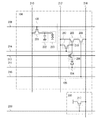
表示装置の構成について、図1を参照して説明する。表示パネル100は、画素回路101、表示素子制御回路102及びフォトセンサ制御回路103を有する。
The structure of the display device will be described with reference to FIG. The
画素回路101は、行列方向にマトリクス状に配置された複数の画素104を有する。各々の画素104は、表示素子105とフォトセンサ106を有する。全ての画素104にフォトセンサを設けず、複数の画素毎に設けてもよい。また、画素104の外にフォトセンサを設けてもよい。
The
画素104の回路図について、図2を用いて説明する。画素104は、トランジスタ201(画素トランジスタともいう)、保持容量202及び液晶素子203を有する表示素子105と、受光素子であるフォトダイオード204、トランジスタ205(第1のトランジスタともいう)、トランジスタ206(第2のトランジスタともいう)、トランジスタ207(第3のトランジスタともいう)、トランジスタ208(第4のトランジスタともいう)を有するフォトセンサ106とを有する。
A circuit diagram of the
表示素子105において、トランジスタ201は、ゲートがゲート信号線209に、ソース又はドレインの一方がビデオデータ信号線210に、ソース又はドレインの他方が保持容量202の一方の電極と液晶素子203の一方の電極に接続されている。保持容量202の他方の電極と液晶素子203の他方の電極は一定の電圧レベルに保たれている。液晶素子203は、一対の電極と、該一対の電極の間に液晶層を含む素子である。
In the
なお、AとBとが接続されている、と明示的に記載する場合は、AとBとが電気的に接続されている場合と、AとBとが機能的に接続されている場合と、AとBとが直接接続されている場合とを含むものとする。 In addition, when it is explicitly described that A and B are connected, A and B are electrically connected, and A and B are functionally connected. , A and B are directly connected.
トランジスタ201は、保持容量202への電荷の注入もしくは放出を制御する機能を有する。例えば、ゲート信号線209に高レベルの電圧が印加されると、ビデオデータ信号線210の電圧レベルの電圧を保持容量202と液晶素子203に印加する。保持容量202は、液晶素子203に印加する電圧に相当する電荷を保持する機能を有する。液晶素子203に電圧を印加することで偏光方向が変化することを利用して、液晶素子203を透過する光の明暗(階調)を作ることで、画像表示が実現される。液晶素子203を透過する光には、光源(バックライト)によって表示装置の裏面から照射される光を用いる。
The
トランジスタ201は、非晶質半導体、微結晶半導体、多結晶半導体、酸化物半導体、又は単結晶半導体などを用いることができる。特に、酸化物半導体を用い、オフ電流が極めて小さいトランジスタとすることで、表示品質を高めることができる。
The
なお、ここでは、表示素子105が液晶素子を有する場合について説明したが、発光素子などの他の素子を有していてもよい。発光素子は、電流または電圧によって輝度が制御される素子であり、具体的には発光ダイオード、OLED(Organic Light Emitting Diode)等が挙げられる。なお本実施の形態の構成では、画素に表示素子105とフォトセンサ106を備えた光学式タッチセンサ(光学式タッチパネルともいう)の構成について示し説明しているが、画素から表示素子を除いた構成とすることもできる。この場合、フォトセンサが複数設けられた、イメージセンサとしての構成とすることができる。
Note that although the case where the
フォトセンサ106において、フォトダイオード204は、一方の電極が配線211(グラウンド線ともいう)に、他方の電極がトランジスタ206のソース又はドレインの一方に接続されている。トランジスタ205は、ソース又はドレインの一方がフォトセンサ基準信号線212に、ソース又はドレインの他方がトランジスタ208のソース又はドレインの一方に接続されている。トランジスタ206は、ゲートがゲート信号線213に、ソース又はドレインの他方がトランジスタ205のゲート、及びトランジスタ207のソース又はドレインの一方に接続されている。トランジスタ207は、ゲートがフォトダイオードリセット信号線214に、ソース又はドレインの他方がフォトセンサ基準信号線212に接続されている。トランジスタ208は、ゲートがゲート信号線215に、ソース又はドレインの他方がフォトセンサ出力信号線216に接続されている。
In the
フォトダイオード204は、非晶質半導体、微結晶半導体、多結晶半導体、酸化物半導体、又は単結晶半導体などを用いることができる。特に、入射光から生成される電気信号の割合(量子効率)を向上させるために、結晶欠陥の少ない単結晶半導体(例えば単結晶シリコン)を用いることが望ましい。また、半導体材料は、結晶性を向上させることが容易であるシリコン又はシリコンゲルマニウム等のシリコン半導体を用いることが好ましい。
The
トランジスタ205は、非晶質半導体、微結晶半導体、多結晶半導体、酸化物半導体、又は単結晶半導体などを用いることができる。特にトランジスタ205は、フォトダイオード204からトランジスタ206を介して供給される電荷をゲートが接続されたノードに蓄積し、蓄積された電荷を出力信号に変換する機能を有する。そのため、単結晶半導体を用い、移動度の高いトランジスタとすることが望ましい。また、半導体材料は、結晶性を向上させることが容易であるシリコン又はシリコンゲルマニウム等のシリコン半導体を用いることが好ましい。
The
トランジスタ206は、非晶質半導体、微結晶半導体、多結晶半導体、酸化物半導体、又は単結晶半導体などを用いることができる。特にトランジスタ206は、トランジスタ206の導通または非導通を制御することにより、トランジスタ205のゲートの電荷を保持する機能を有する。そのため、酸化物半導体を用い、オフ電流が極めて小さいトランジスタとすることが好ましい。
The
トランジスタ207は、非晶質半導体、微結晶半導体、多結晶半導体、酸化物半導体、又は単結晶半導体などを用いることができる。特にトランジスタ207は、トランジスタ207の導通または非導通を制御することにより、トランジスタ205のゲートの電荷を放電する機能、及びゲートの電荷を保持する機能を有する。そのため、酸化物半導体を用い、オフ電流が極めて小さいトランジスタとすることが好ましい。
The
トランジスタ208は、非晶質半導体、微結晶半導体、多結晶半導体、酸化物半導体、又は単結晶半導体などを用いることができる。特にトランジスタ208は、フォトセンサ出力信号線216にトランジスタ205の出力信号を供給する機能を有するため、単結晶半導体を用い、移動度の高いトランジスタとすることが望ましい。また、半導体材料は、結晶性を向上させることが容易であるシリコン又はシリコンゲルマニウム等のシリコン半導体を用いることが好ましい。
The
表示素子制御回路102は、表示素子105を制御するための回路であり、ビデオデータ信号線などの信号線(「ソース信号線」ともいう。)を介して表示素子105に信号を入力する表示素子駆動回路107と、走査線(「ゲート信号線」ともいう。)を介して表示素子105に信号を入力する表示素子駆動回路108を有する。例えば、走査線側の表示素子駆動回路108は、特定の行に配置された画素が有する表示素子を選択する機能を有する。また、信号線側の表示素子駆動回路107は、選択された行の画素が有する表示素子に任意のレベルの電圧を与える機能を有する。なお、走査線側の表示素子駆動回路108によりゲート信号線に高レベルの電圧を印加された表示素子105では、トランジスタが導通状態となり、信号線側の表示素子駆動回路107によりビデオデータ信号線に与えられる電圧レベルの電圧が供給される。
The display
フォトセンサ制御回路103は、フォトセンサ106を制御するための回路であり、フォトセンサ出力信号線、フォトセンサ基準信号線等の信号線側のフォトセンサ読み出し回路109と、走査線側のフォトセンサ駆動回路110を有する。
The
フォトセンサ駆動回路110は、特定の行に配置された画素が有するフォトセンサ106に対して、後述するリセット動作と累積動作と選択動作とを行う機能を有する。
The
また、フォトセンサ読み出し回路109は、選択された行の画素が有するフォトセンサ106の出力信号を取り出す機能を有する。なお、フォトセンサ読み出し回路109は、アナログ信号であるフォトセンサ106の出力を、OPアンプを用いてアナログ信号のまま表示パネル外部に取り出す。もしくは、A/D変換回路を用いてデジタル信号に変換してから表示パネル外部に取り出す。
The
フォトセンサ読み出し回路109を構成するプリチャージ回路について、図2を用いて説明する。図2において、画素1列分のプリチャージ回路200は、トランジスタ217、プリチャージ信号線218から構成される。なお、プリチャージ回路200の後段に、OPアンプやA/D変換回路を接続して、フォトセンサ読み出し回路109を構成することができる。
A precharge circuit included in the
プリチャージ回路200では、画素内におけるフォトセンサの動作に先立ち、フォトセンサ出力信号線の電圧レベルを基準電圧レベルに設定する。図2では、プリチャージ信号線218をHレベル(以下、”H”と略記)とし、トランジスタ217を導通させることで、フォトセンサ出力信号線216の電圧レベルを基準電圧レベル(ここでは低電圧レベルとする)に設定することができる。なお、フォトセンサ出力信号線216の電圧レベルを安定させるために、フォトセンサ出力信号線216に保持容量を設けることも有効である。なお、基準電圧レベルは、高電圧レベルとする構成とすることができる。この場合、トランジスタ217は、図2と逆極性とし、プリチャージ信号線218をLレベル(以下、”L”と略記)とすることで、フォトセンサ出力信号線216の電圧レベルを基準電圧レベルに設定することができる。
In the
なお、本実施の形態におけるHレベル、及びLレベルの電圧レベルとは、それぞれ、高電源電圧レベルに基づく電圧レベル、低電源電圧レベルに基づく電圧レベルに相当する。すなわち、Hレベルであれば、3V乃至20Vの定電圧であり、Lレベルであれば、0V(基準電圧レベル、グラウンド電圧レベルともいう)の定電圧である。 Note that the H level and L level voltage levels in this embodiment correspond to a voltage level based on a high power supply voltage level and a voltage level based on a low power supply voltage level, respectively. That is, if it is H level, it is a constant voltage of 3V to 20V, and if it is L level, it is a constant voltage of 0V (also referred to as a reference voltage level or a ground voltage level).
次に、フォトセンサ106の動作について、図3のタイミングチャートを用いて説明する。図3において、信号301、信号302、信号303は、図2におけるゲート信号線213、リセット信号線214、ゲート信号線215の電圧レベルに相当する。また信号304A乃至304Cは、トランジスタ205のゲートの電圧レベル(図2中のノード219の電圧レベル)に相当し、信号304Aがフォトダイオード204に入射される光の照度が大きい場合(以下、照度大)、信号304Bがフォトダイオード204に入射される光の照度が中程度の場合(以下、照度中)、信号304Cがフォトダイオード204に入射される光の照度が小さい場合(以下、照度小)について表している。また、信号305A乃至305Cは、フォトセンサ出力信号線216の電圧レベルに相当し、信号305Aが照度大、信号305Bが照度中、信号305Cが照度小について表している。
Next, the operation of the photosensor 106 will be described with reference to the timing chart of FIG. 3, signals 301, 302, and 303 correspond to the voltage levels of the
期間Aにおいて、ゲート信号線213の電圧レベル(信号301)を”H”、リセット信号線214の電圧レベル(信号302)を0V未満の電圧レベル(以下”L2”と略記)、ゲート信号線215の電圧レベル(信号303)を”L”、とする。次いで、期間Bにおいて、ゲート信号線213の電圧レベル(信号301)を”H”、リセット信号線214の電圧レベル(信号302)を”H”、ゲート信号線215の電圧レベル(信号303)を”L”、とする。その結果、フォトダイオード204が導通及びトランジスタ206が導通状態となり、ノード219の電圧レベル(信号304A乃至304C)が”H”となる。このとき、フォトダイオード204には逆バイアスが印加される状態となる。また、プリチャージ信号線218の電圧レベルをHレベルとすると、フォトセンサ出力信号線216の電圧レベル(信号305A乃至信号305C)は”L”にプリチャージされる。以上、期間A、期間Bがリセット動作期間となる。
In the period A, the voltage level of the gate signal line 213 (signal 301) is “H”, the voltage level of the reset signal line 214 (signal 302) is a voltage level lower than 0V (hereinafter abbreviated as “L2”), and the
なお、本明細書において、0V未満の電圧レベルとは、具体的には、トランジスタ206及びトランジスタ207のソースの電圧レベル及びドレインの電圧レベルより小さい電圧レベルのことをいう。本実施の形態では、トランジスタ206及びトランジスタ207のソース及びドレインの低電圧の側の電圧レベルは、グラウンド線の電圧レベルとなる0Vであり、所定の期間におけるゲート信号線213の電圧レベル、リセット信号線214の電圧レベルを、0V未満の電圧レベルと呼ぶことがある。また、トランジスタ206及びトランジスタ207のソース及びドレインの低電圧の側の電圧レベルは、図2に示す回路構成に基づいて、フォトダイオード204に接続された配線211の電圧レベル及びフォトセンサ基準信号線212の電圧レベルと換言することもできる。
Note that in this specification, the voltage level lower than 0 V specifically means a voltage level lower than the voltage level of the source and the drain of the
次いで期間Cにおいて、ゲート信号線213の電圧レベル(信号301)を”H”、リセット信号線214の電圧レベル(信号302)を”L2”、ゲート信号線215の電圧レベル(信号303)を”L”、とする。その結果、フォトダイオード204への光照射による電流(以下、光電流という)により、ノード219の電圧レベル(信号304A乃至304C)が低下し始める。フォトダイオード204は、入射光の光量の増加に応じて光電流が増加するので、入射光の光量に応じてノード219の電圧レベル(信号304A乃至304C)は変化する。具体的には、入射光の光量が大きい信号304Aでは、光電流が大きく増加することで、ノード219の電圧レベルである信号304Aは、期間Cで大きく減少することとなる。また入射光の光量が小さい信号304Cでは、光電流がほとんど流れないことで、ノード219の電圧レベルである信号304Cは、期間Cでほとんど変化しないこととなる。また入射光の光量が中程度の信号304Bでは、光電流が信号304Aと信号304Cでの中間程度に増加することで、ノード219の電圧レベルである信号304Bは、信号304Aと信号304Cでの中間程度に減少することとなる。すなわち、フォトダイオード204は、入射光に応じてトランジスタ205のゲートに対し、トランジスタ206を介して、電荷を供給する機能を有している。そして、トランジスタ205のソースとドレイン間のチャネル抵抗が変化する。以上期間Cが累積動作期間となる。
Next, in period C, the voltage level of the gate signal line 213 (signal 301) is “H”, the voltage level of the reset signal line 214 (signal 302) is “L2”, and the voltage level of the gate signal line 215 (signal 303) is “ L ". As a result, a voltage level (signals 304A to 304C) of the
次いで期間Dにおいて、ゲート信号線213の電圧レベル(信号301)を”L2”、リセット信号線214の電圧レベル(信号302)を”L2”、ゲート信号線215の電圧レベル(信号303)を”L”、とする。ノード219の電圧レベルである信号304A乃至304Cは一定となる。ここで、期間Dでの信号304A乃至304Cの電圧レベルは、前述の累積動作期間(期間C)中にフォトダイオード204の光電流の大きさにより決まる。すなわち、フォトダイオード204への入射光に応じてノード219に蓄積される電荷が変化する。なお、トランジスタ206及びトランジスタ207の半導体層には、酸化物半導体を用い、オフ電流が極めて小さいトランジスタとすることにより、後の選択動作を行うまで、蓄積された電荷を一定に保つことができる。
Next, in period D, the voltage level of the gate signal line 213 (signal 301) is “L2”, the voltage level of the reset signal line 214 (signal 302) is “L2”, and the voltage level of the gate signal line 215 (signal 303) is “ L ".
次いで期間Eにおいて、ゲート信号線213の電圧レベル(信号301)を”L2”、リセット信号線214の電圧レベル(信号302)を”L2”、ゲート信号線215の電圧レベル(信号303)を”H”、とする。その結果、トランジスタ208が導通し、フォトセンサ基準信号線212とフォトセンサ出力信号線216とが、トランジスタ205とトランジスタ208とを介して導通する。すると、フォトセンサ出力信号線216の電圧レベル(信号305A乃至305C)は、前述のフォトダイオード204への入射光に応じて上昇していく。なお、期間Eより前の期間で、プリチャージ信号線218の電圧レベルは”H”とし、フォトセンサ出力信号線216のプリチャージを終了しておく。ここで、フォトセンサ出力信号線216の電圧レベル(信号305A乃至305C)が上昇する速さは、トランジスタ205のソースとドレイン間を流れる電流に依存する。すなわち、累積動作期間である期間C中にフォトダイオード204に照射されている入射光の光量に応じて変化する。以上、期間Eが選択動作期間である。
Next, in period E, the voltage level of the gate signal line 213 (signal 301) is “L2”, the voltage level of the reset signal line 214 (signal 302) is “L2”, and the voltage level of the gate signal line 215 (signal 303) is “ H ”. As a result, the
次いで期間Fにおいて、ゲート信号線213の電圧レベル(信号301)を”L2”、リセット信号線214の電圧レベル(信号302)を”L2”、ゲート信号線215の電圧レベル(信号303)を”L”、とする。その結果、トランジスタ208が非導通状態となり、フォトセンサ出力信号線216の電圧レベル(信号305A乃至305C)は、一定値となる。ここで、一定値となる値は、フォトダイオード204に照射されている入射光の光量に応じて決まる.従って、フォトセンサ出力信号線216の電圧レベルを取得することで、累積動作中におけるフォトダイオード204への入射光の量を知ることができる。以上、期間Fが読み取り動作期間である。
Next, in the period F, the voltage level of the gate signal line 213 (signal 301) is “L2”, the voltage level of the reset signal line 214 (signal 302) is “L2”, and the voltage level of the gate signal line 215 (signal 303) is “ L ". As a result, the
以上説明したように、本実施の形態における半導体装置は、トランジスタ206の非導通状態の期間となる期間D、期間E、及び期間F、並びにトランジスタ207の非導通状態の期間となる期間A、期間D、期間E、及び期間Fにおいて、トランジスタ206及びトランジスタ207のゲートに印加される電圧の電圧レベルを0V未満とすることを特徴とする。すなわち、トランジスタ206のゲートとソースの間に印加される電圧の電圧レベルをトランジスタ206のしきい値電圧以下、及びトランジスタ207のゲートとソースの間に印加される電圧の電圧レベルを、トランジスタ207のしきい値電圧以下となる電圧レベルとすることを特徴とする。その結果、トランジスタ205のゲートに保持された電荷を保持する機能を向上することができる。
As described above, the semiconductor device in this embodiment includes the period D, the period E, and the period F in which the
より具体的にいえば、個々のフォトセンサの動作は、リセット動作と累積動作と選択動作と読み取り動作とを繰り返すことで実現される。上述したように、本実施の形態におけるトランジスタ206及びトランジスタ207は、非導通状態とする期間において、ゲートに印加される電圧の電圧レベルを0V未満とするものである。そのためトランジスタ206及びトランジスタ207の非導通状態をより確実に行うことができ、累積動作及び読み取り動作時にトランジスタ205のゲートに保持された電荷を保持する機能を向上することができる。またフォトセンサにおける入射光を正確に電気信号に変換できるといった機能を向上させることができる。さらにトランジスタ206及びトランジスタ207の半導体層を酸化物半導体を用いて形成し、オフ電流を極めて小さくする構成も好適である。当該構成により、フォトセンサにおける入射光をより正確に電気信号に変換できるといった機能を向上させることができる。
More specifically, the operation of each photosensor is realized by repeating a reset operation, an accumulation operation, a selection operation, and a reading operation. As described above, the voltage level of the voltage applied to the gate of the
本実施の形態は、他の実施の形態と適宜組み合わせて実施することができる。 This embodiment can be implemented in appropriate combination with any of the other embodiments.
(実施の形態2)
本実施の形態では、複数のフォトセンサを用いた場合の駆動方法について説明する。
(Embodiment 2)
In this embodiment, a driving method in the case of using a plurality of photosensors will be described.
まず、図4に示すタイミングチャートのような駆動方法を考える。図4において、信号401、信号402、信号403は、各々第1行、第2行、第3行のフォトセンサにおけるリセット信号線214の電位変化を示す信号である。また、信号404、信号405、信号406は、各々第1行、第2行、第3行のフォトセンサにおけるゲート信号線213の電位変化を示す信号である。また、信号407、信号408、信号409は、各々第1行、第2行、第3行のフォトセンサにおけるゲート信号線215の電位変化を示す信号である。期間410は、1回の撮像に要する期間である。また、期間411、期間412、期間413は、第2行のフォトセンサが、各々リセット動作、累積動作、選択動作を行っている期間である。このように、各行のフォトセンサを順に駆動していくことで、撮像が可能になる。
First, a driving method like the timing chart shown in FIG. 4 is considered. In FIG. 4, a
ここで、各行のフォトセンサにおける累積動作について、時間的なズレが生じていることがわかる。すなわち、各行のフォトセンサにおける撮像の同時性が損なわれる。そのため、撮像画像に歪みが生じることになる。特に、第1行から第3行の方向に高速に移動する被検出物に対しては、尾を引くように、拡大されたような形状の撮像画像になり、逆方向に移動する被検出物に対しては、縮小されたような形状の撮像画像になるなど、形状が歪みやすい。 Here, it can be seen that there is a temporal shift in the cumulative operation of the photosensors in each row. That is, the image capturing synchronism of the photosensors in each row is impaired. For this reason, the captured image is distorted. In particular, for a detection object that moves at high speed in the direction from the first row to the third row, the detection object that has a captured image with an enlarged shape so as to draw a tail and moves in the opposite direction On the other hand, the shape tends to be distorted, such as a captured image having a reduced shape.
各行のフォトセンサにおける累積動作に時間的なズレを生じさせないためには、各行のフォトセンサを順に駆動する周期を短くすることが有効である。しかしながら、この場合、フォトセンサの出力信号をOPアンプもしくはA/D変換回路で非常に高速度に取得する必要がある。したがって、消費電力の増大を招く。特に、高解像度の画像を取得する場合には、非常に困難となる。 In order not to cause a time shift in the cumulative operation of the photosensors in each row, it is effective to shorten the cycle for sequentially driving the photosensors in each row. However, in this case, it is necessary to acquire the output signal of the photosensor at an extremely high speed by an OP amplifier or an A / D conversion circuit. Therefore, power consumption is increased. In particular, it is very difficult to acquire a high-resolution image.
そこで、図5に示すタイミングチャートのような駆動方法を提案する。図5において、信号501、信号502、信号503は、各々第1行、第2行、第3行のフォトセンサにおけるリセット信号線214の電位変化を示す信号である。また、信号504、信号505、信号506は、各々第1行、第2行、第3行のフォトセンサにおけるゲート信号線213の電位変化を示す信号である。また、信号507、信号508、信号509は、各々第1行、第2行、第3行のフォトセンサにおけるゲート信号線215の電位変化を示す信号である。期間510は、1回の撮像に要する期間である。また、期間511、期間512、期間513は、第2行のフォトセンサが、各々リセット動作(他の行でも共通)、累積動作(他の行でも共通)、選択動作を行っている期間である。
Therefore, a driving method like the timing chart shown in FIG. 5 is proposed. In FIG. 5, a
図5において、図4と異なるのは、全行のフォトセンサについて、リセット動作と累積動作とが共通の時間に行われ、累積動作終了後に累積動作とは非同期に、各行で順に選択動作を行う点である。累積動作を共通の期間にすることで、各行のフォトセンサにおける撮像の同時性が確保され、高速に移動する被検出物に対しても、歪みが少ない画像を容易に得ることができる。累積動作を共通にすることで、各フォトセンサのリセット信号線214の駆動回路を共通にすることができる。また、各フォトセンサのゲート信号線213の駆動回路も共通にすることができる。このように駆動回路を共通にすることは、周辺回路の削減や低消費電力化に有効である。さらに、選択動作を各行で順次行うことで、フォトセンサの出力信号を取得する際に、OPアンプもしくはA/D変換回路の動作速度を遅くすることができる。その際、選択動作に要する合計の時間を、累積動作に要する時間より長くすることが好ましい。特に、高解像度の画像を取得する場合には、非常に有効である。
In FIG. 5, the difference from FIG. 4 is that the reset operation and the accumulation operation are performed at a common time for the photosensors of all the rows, and the selection operation is sequentially performed in each row asynchronously with the accumulation operation after the accumulation operation is completed. Is a point. By setting the cumulative operation to a common period, the synchronization of imaging in the photosensors in each row is ensured, and an image with little distortion can be easily obtained even for a detection object that moves at high speed. By making the cumulative operation common, the drive circuit of the
なお、図5では、各行のフォトセンサを順次駆動する駆動方法について、タイミングチャートを示したが、特定の領域における画像を取得するために、特定の行におけるフォトセンサのみを順次駆動する駆動方法も有効である。これにより、OPアンプもしくはA/D変換回路の動作を軽減し、消費電力を低減しながら、必要な画像を取得することができる。また、数行おきにフォトセンサを駆動する駆動方法も有効である。すなわち、複数のフォトセンサの一部を駆動させる。これにより、OPアンプもしくはA/D変換回路の動作を軽減し、消費電力を低減しながら、必要な解像度の画像を取得することができる。 Note that FIG. 5 shows the timing chart for the driving method for sequentially driving the photosensors in each row, but there is also a driving method for sequentially driving only the photosensors in a specific row in order to acquire an image in a specific region. It is valid. Thereby, the operation of the OP amplifier or the A / D conversion circuit can be reduced, and a necessary image can be acquired while reducing power consumption. A driving method for driving the photosensors every several rows is also effective. That is, some of the plurality of photosensors are driven. Thereby, the operation of the OP amplifier or the A / D conversion circuit can be reduced, and an image with a necessary resolution can be acquired while reducing power consumption.
以上のような駆動方法を実現するためには、累積動作が終了した後も、各フォトセンサにおけるトランジスタ205のゲートの電圧レベルを一定に保つ必要がある。したがって、上記実施の形態で説明したように、トランジスタ207は、酸化物半導体を用いて形成され、オフ電流が極めて小さいことが好ましい。
In order to realize the above driving method, it is necessary to keep the voltage level of the gate of the
以上のような形態とすることで、高速で移動する被検出物に対しても歪みが少なく、高解像度の撮像が実現でき、且つ低消費電力の表示装置又は半導体装置を提供することができる。 With the above configuration, a display device or a semiconductor device with little distortion even for an object to be detected that moves at high speed, high-resolution imaging, and low power consumption can be provided.
本実施の形態は、他の実施の形態と適宜組み合わせて実施することができる。 This embodiment can be implemented in appropriate combination with any of the other embodiments.
(実施の形態3)
本実施の形態では、図2におけるフォトセンサ106の回路構成の変形例について説明する。
(Embodiment 3)
In this embodiment, a modification of the circuit configuration of the photosensor 106 in FIG. 2 will be described.
図6(A)は、図2においてトランジスタ205のゲートに接続された、フォトセンサのリセット動作を制御するためのトランジスタ207を省略した構成を示している。図6(A)の構成では、フォトセンサのリセット動作を行う際、配線211の電圧レベルを変化させることでトランジスタ205のゲートに蓄積された電荷の放電を行う構成とすればよい。
FIG. 6A illustrates a structure in which the
図6(B)は、図2におけるフォトセンサ106の構成においてトランジスタ205とトランジスタ208との接続関係を逆にした構成を示している。具体的には、トランジスタ205のソース又はドレインの一方がフォトセンサ出力信号線216に接続され、トランジスタ208のソース又はドレインの一方が、フォトセンサ基準信号線212に接続されている。
FIG. 6B illustrates a structure in which the connection relation between the
図6(C)は、図2におけるフォトセンサ106の構成においてトランジスタ208を省略した構成を示す。図6(C)の構成では、上記説明した図2、図6(A)、(B)とは異なり、フォトセンサの選択動作及び読み取り動作を行う際、フォトセンサ基準信号線212の電圧レベルを変化させることでトランジスタ205のゲートに蓄積された電荷に応じた信号の変化を読み取る構成とすればよい。
FIG. 6C illustrates a structure in which the
図6(C)に示すフォトセンサ106の動作に関し、タイミングチャートを図10に示す。図10において、信号601、信号602、信号603は、図6(C)におけるゲート信号線213、リセット信号線214、フォトセンサ基準信号線212の電圧レベルに相当する。また信号604は、トランジスタ205のゲートの電圧レベルに相当し、フォトダイオード204に入射される光の照度が中程度の場合(以下、照度中)について表している。また、信号605は、フォトセンサ出力信号線216の電圧レベルについて表している。また、信号606は、図6(C)中のノード611の電圧レベルについて表している。
FIG. 10 is a timing chart regarding the operation of the photosensor 106 illustrated in FIG. In FIG. 10, signals 601, 602, and 603 correspond to the voltage levels of the
次いで図10のタイミングチャートについて説明する。期間Aにおいて、信号601と信号603の電圧レベルを”H”、信号602の電圧レベルを”L2”にする。そして期間Bにおいて、信号602の電圧レベルを”H”にすると、信号604の電圧レベルがリセットされ、信号605及び信号606の電圧レベルが上昇する。以上、期間A、期間Bがリセット動作期間となる。次いで、期間Cにおいて、信号601の電圧レベルを”L2”にすると、信号606の電圧レベルが下降する。そして期間Dにおいて、信号602及び信号603の電圧レベルを”L2”にする。以上、期間C、期間Dが累積動作期間となる。次いで、期間Eにおいて、信号601と信号603の電圧レベルを”H”にすると、信号604と信号606との電圧レベルが同じ電圧レベルとなり、信号605ではフォトセンサの出力信号に応じて電圧レベルが変化する。以上期間Eが選択動作期間となる。そして期間Fにおいて、信号601と信号603の電圧レベルを”L2”にし、信号605の電圧レベルを読み取る。以上、期間Fが読み取り動作期間である。以上のようにして、図6(C)に示すフォトセンサ106を動作させればよい。
Next, the timing chart of FIG. 10 will be described. In the period A, the voltage levels of the
本実施の形態は、他の実施の形態と適宜組み合わせて実施することができる。 This embodiment can be implemented in appropriate combination with any of the other embodiments.
(実施の形態4)
本実施の形態では、フォトセンサを有する半導体装置の構造及び作製方法について説明する。図7に半導体装置の断面図を示す。なお、表示装置を構成する場合も、以下の半導体装置を用いることができる。
(Embodiment 4)
In this embodiment, a structure and manufacturing method of a semiconductor device including a photosensor will be described. FIG. 7 shows a cross-sectional view of the semiconductor device. Note that the following semiconductor device can also be used in the case of forming a display device.
図7では、絶縁表面を有する基板1001上に、フォトダイオード1002、トランジスタ1003、及びトランジスタ1004が設けられている。それぞれ、図2における、フォトダイオード204、トランジスタ205、及びトランジスタ206の断面図を示している。被検出物1201から発せられる光1202、被検出物1201で外光が反射した光1202、又は装置内部から発せられた光が被検出物1201で反射した光1202が、フォトダイオード1002に入射される。基板1001側の被検出物を撮像する構成としてもよい。
In FIG. 7, a
基板1001は、絶縁性基板(例えばガラス基板又はプラスチック基板)、該絶縁性基板上に絶縁膜(例えば酸化珪素膜又は窒化珪素膜)を形成したもの、半導体基板(例えばシリコン基板)上に該絶縁膜を形成したもの、又は金属基板(例えばアルミニウム基板)上に該絶縁膜を形成したものを用いることができる。
The
フォトダイオード1002は、横型接合タイプのpinダイオードであり、半導体膜1005を有している。半導体膜1005は、p型の導電性を有する領域(p層1021)と、i型の導電性を有する領域(i層1022)と、n型の導電性を有する領域(n層1023)とを有している。なお、フォトダイオード1002は、pnダイオードであっても良い。
The
横型接合タイプのpinダイオード又はpnダイオードは、p型を付与する不純物と、n型を付与する不純物とを、それぞれ半導体膜1005の特定の領域に添加することで、形成することが出来る。
A lateral junction type pin diode or pn diode can be formed by adding an impurity imparting p-type conductivity and an impurity imparting n-type conductivity to specific regions of the
フォトダイオード1002は、入射光から生成される電気信号の割合(量子効率)を向上させるために、結晶欠陥の少ない単結晶半導体(例えば単結晶シリコン)を用いて半導体膜1005を形成することが好ましい。
In the
トランジスタ1003は、トップゲート型の薄膜トランジスタであり、半導体膜1006、ゲート絶縁膜1007、及びゲート電極1008を有している。
The
トランジスタ1003は、フォトダイオード1002から供給される電荷を出力信号に変換する機能を有する。そのため、単結晶半導体(例えば単結晶シリコン)を用いて半導体膜1006を形成し、移動度の高いトランジスタとすることが好ましい。
The
半導体膜1005及び半導体膜1006を、単結晶半導体を用いて形成する例を示す。単結晶半導体基板(例えば単結晶シリコン基板)の所望の深さに、イオン照射等を行い損傷領域を形成する。当該単結晶半導体基板と基板1001とを絶縁膜を介して貼り合わせた後、損傷領域から単結晶半導体基板を分離して、基板1001上に半導体膜を形成する。当該半導体膜をエッチングなどにより所望の形状に加工(パターニング)することで、半導体膜1005及び半導体膜1006を形成する。半導体膜1005と半導体膜1006を同一工程で形成することができるため、コストを低減できる。これにより、フォトダイオード1002とトランジスタ1003とは同一表面上に形成されることになる。
An example in which the
なお、半導体膜1005及び半導体膜1006は、非晶質半導体、微結晶半導体、多結晶半導体、酸化物半導体などを用いて形成することもできる。特に、単結晶半導体を用いることで移動度の高いトランジスタとすることが望ましい。また、半導体材料は、結晶性を向上させることが容易であるシリコン又はシリコンゲルマニウム等のシリコン半導体を用いることが好ましい。
Note that the
ここで、フォトダイオード1002の量子効率を向上させるため、半導体膜1005を厚く形成することが好ましい。更に、トランジスタ1003のS値等の電気特性を良好にするため、半導体膜1006を薄く形成することが好ましい。この場合、半導体膜1005は、半導体膜1006より厚く形成すればよい。
Here, in order to improve the quantum efficiency of the
また、図2におけるトランジスタ208についても、結晶性半導体を用い、移動度が高いトランジスタとすることが望ましい。トランジスタ1003と同じ半導体材料を用いることで、トランジスタ1003と同一工程で形成することができ、コストを低減できる。
2 is preferably a transistor which uses a crystalline semiconductor and has high mobility. By using the same semiconductor material as the
なお、ゲート絶縁膜1007は、酸化珪素膜又は窒化珪素膜等を用いて、単層又は積層で形成する。プラズマCVD法又はスパッタリング法を用いて形成すればよい。
Note that the
なお、ゲート電極1008は、モリブデン、チタン、クロム、タンタル、タングステン、アルミニウム、銅、ネオジム、スカンジウム等の金属材料、又はこれらを主成分とする合金材料を用いて、単層又は積層で形成する。スパッタリング法又は真空蒸着法を用いて形成すればよい。
Note that the
また、フォトダイオード1002は、横型接合タイプとせずに、p層、i層、及びn層を積層させた構造を採用することもできる。また、トランジスタ1003は、ボトムゲート型としてもよく、チャネルストップ構造又はチャネルエッチ構造とすることもできる。
Further, the
なお、図9のように、フォトダイオード1002の下部に遮光膜1301を設け、検出すべき光以外を遮る構成としてもよい。フォトダイオード1002の上部に遮光膜を設けてもよい。その場合、フォトダイオード1002が形成された基板1001と対向する基板1302に遮光膜を設ければよい。
Note that as illustrated in FIG. 9, a
トランジスタ1004は、ボトムゲート型の逆スタガ構造の薄膜トランジスタであり、ゲート電極1010、ゲート絶縁膜1011、半導体膜1012、電極1013、電極1014を有する。また、トランジスタ1004上に絶縁膜1015を有する。なお、トランジスタ1004は、トップゲート型としてもよい。
The
ここでトランジスタ1004は、フォトダイオード1002及びトランジスタ1003の上方に絶縁膜1009を介して形成されていることを特徴とする。このようにトランジスタ1004をフォトダイオード1002と異なる層に形成することで、フォトダイオード1002の面積を拡大することが可能となり、フォトダイオード1002の受光量を大きくすることができる。
Here, the
また、トランジスタ1004の一部又は全部が、フォトダイオード1002のn層1023又はp層1021のいずれかと重なるように形成することが好ましい。フォトダイオード1002の面積を拡大できるとともに、トランジスタ1004とi層1022との重なりを極力小さくすることで効率よく受光を行うことができるからである。pnダイオードの場合も、トランジスタ1004とpn接合部との重なりを小さくすることで効率よく受光を行うことができる。
In addition, part or all of the
トランジスタ1004は、フォトダイオード1002の出力信号をトランジスタ1003のゲートに電荷として累積し、また、当該電荷を保持する機能を有する。そのため、酸化物半導体を用いて半導体膜1012を形成し、オフ電流が極めて低いトランジスタとすることが好ましい。
The
また、図2におけるトランジスタ207についても、酸化物半導体を用いたオフ電流が極めて低いトランジスタを用いることが望ましい。トランジスタ1004と同じ半導体材料を用いることで、トランジスタ1004と同一工程で形成することができ、コストを低減できる。なお、上記の各半導体素子について、薄膜半導体を用いても、バルク半導体を用いてもよい。
2 is preferably a transistor with an extremely low off-state current using an oxide semiconductor. By using the same semiconductor material as the
以下に、半導体膜1012を、酸化物半導体を用いて形成する例を示す。
An example in which the
トランジスタのオフ電流を大きくする要因として、酸化物半導体中に水素等の不純物(例えば水素、水、又は水酸基)が含まれていることが挙げられる。水素等は、酸化物半導体中でキャリアの供与体(ドナー)になる可能性があり、オフ状態においても電流を発生させる要因となる。すなわち、酸化物半導体中に水素等が多量に含まれていると、酸化物半導体がN型化されてしまう。 As a factor for increasing the off-state current of the transistor, an oxide semiconductor includes an impurity such as hydrogen (eg, hydrogen, water, or a hydroxyl group). Hydrogen or the like can be a carrier donor in the oxide semiconductor, and causes current to be generated even in an off state. In other words, when an oxide semiconductor contains a large amount of hydrogen or the like, the oxide semiconductor is N-type.
そこで、以下で示す作製方法は、酸化物半導体中の水素を極力低減し、且つ、構成元素である酸素の濃度を高くすることで、酸化物半導体を高純度化するものである。高純度化された酸化物半導体は、真性又は実質的に真性な半導体であり、オフ電流を小さくすることができる。 Therefore, the manufacturing method described below is to purify an oxide semiconductor by reducing hydrogen in the oxide semiconductor as much as possible and increasing the concentration of oxygen which is a constituent element. A highly purified oxide semiconductor is an intrinsic or substantially intrinsic semiconductor and can reduce off-state current.
まず、絶縁膜1009上に、酸化物半導体膜をスパッタリング法により形成する。
First, an oxide semiconductor film is formed over the insulating
酸化物半導体膜のターゲットとしては、酸化亜鉛を主成分とする金属酸化物のターゲットを用いることができる。例えば、組成比として、In2O3:Ga2O3:ZnO=1:1:1、すなわち、In:Ga:Zn=1:1:0.5のターゲットを用いることができる。また、In:Ga:Zn=1:1:1、又はIn:Ga:Zn=1:1:2の組成比を有するターゲットを用いることもできる。また、SiO2を2重量%以上10重量%以下含むターゲットを用いることもできる。 As a target for the oxide semiconductor film, a metal oxide target containing zinc oxide as a main component can be used. For example, as a composition ratio, a target of In 2 O 3 : Ga 2 O 3 : ZnO = 1: 1: 1, that is, In: Ga: Zn = 1: 1: 0.5 can be used. Alternatively, a target having a composition ratio of In: Ga: Zn = 1: 1: 1 or In: Ga: Zn = 1: 1: 2 can be used. A target containing 2 wt% or more and 10 wt% or less of SiO 2 can also be used.
なお、酸化物半導体膜の成膜の際は、希ガス(代表的にはアルゴン)雰囲気下、酸素雰囲気下、または希ガス及び酸素混合雰囲気下とすればよい。ここで、酸化物半導体膜を成膜する際に用いるスパッタガスは、水素、水、水酸基又は水素化物などの不純物の濃度がppmレベル、好ましくはppbレベルまで除去された高純度ガスを用いる。 Note that the oxide semiconductor film may be formed in a rare gas (typically argon) atmosphere, an oxygen atmosphere, or a rare gas and oxygen mixed atmosphere. Here, as a sputtering gas used for forming the oxide semiconductor film, a high-purity gas from which the concentration of impurities such as hydrogen, water, a hydroxyl group, or hydride is removed to the ppm level, preferably the ppb level is used.
酸化物半導体膜は、処理室内の残留水分を除去しつつ水素及び水分が除去されたスパッタガスを導入して成膜する。処理室内の残留水分を除去するためには、吸着型の真空ポンプを用いることが好ましい。例えば、クライオポンプ、イオンポンプ、チタンサブリメーションポンプを用いることが好ましい。 The oxide semiconductor film is formed by introducing a sputtering gas from which hydrogen and moisture are removed while moisture remaining in the treatment chamber is removed. In order to remove moisture remaining in the treatment chamber, an adsorption-type vacuum pump is preferably used. For example, it is preferable to use a cryopump, an ion pump, or a titanium sublimation pump.
酸化物半導体膜の膜厚は、2nm以上200nm以下とすればよく、好ましくは5nm以上30nm以下とする。そして、酸化物半導体膜にエッチング等を行い、所望の形状に加工(パターニング)して半導体膜1012とする。
The thickness of the oxide semiconductor film may be 2 nm to 200 nm, preferably 5 nm to 30 nm. Then, etching or the like is performed on the oxide semiconductor film and processed (patterned) into a desired shape, whereby the
以上では、酸化物半導体膜としてIn−Ga−Zn−Oを用いる例を示したが、その他にも、In−Sn−Ga−Zn−O、In−Sn−Zn−O、In−Al−Zn−O、Sn−Ga−Zn−O、Al−Ga−Zn−O、Sn−Al−Zn−O、In−Zn−O、Sn−Zn−O、Al−Zn−O、Zn−Mg−O、Sn−Mg−O、In−Mg−O、In−O、Sn−O、又はZn−Oなどを用いることができる。また、上記酸化物半導体膜はSiを含んでいてもよい。また、これらの酸化物半導体膜は、非晶質であってもよいし、結晶質であってもよい。または、非単結晶であってもよいし、単結晶であってもよい。 Although an example in which In—Ga—Zn—O is used as the oxide semiconductor film is described above, other examples include In—Sn—Ga—Zn—O, In—Sn—Zn—O, and In—Al—Zn. -O, Sn-Ga-Zn-O, Al-Ga-Zn-O, Sn-Al-Zn-O, In-Zn-O, Sn-Zn-O, Al-Zn-O, Zn-Mg-O Sn-Mg-O, In-Mg-O, In-O, Sn-O, Zn-O, or the like can be used. The oxide semiconductor film may contain Si. In addition, these oxide semiconductor films may be amorphous or crystalline. Alternatively, it may be a non-single crystal or a single crystal.
また、酸化物半導体膜として、InMO3(ZnO)m(m>0)で表記される薄膜を用いることもできる。ここで、Mは、Ga、Al、MnおよびCoから選ばれた一または複数の金属元素である。例えば、Mとして、Ga、Ga及びAl、Ga及びMn、またはGa及びCoが挙げられる。 Alternatively, a thin film represented by InMO 3 (ZnO) m (m> 0) can be used as the oxide semiconductor film. Here, M is one or more metal elements selected from Ga, Al, Mn, and Co. For example, M includes Ga, Ga and Al, Ga and Mn, or Ga and Co.
次に、酸化物半導体膜(半導体膜1012)に第1の加熱処理を行う。第1の加熱処理の温度は、400℃以上750℃以下、好ましくは400℃以上基板の歪み点未満とする。 Next, first heat treatment is performed on the oxide semiconductor film (semiconductor film 1012). The temperature of the first heat treatment is 400 ° C. or higher and 750 ° C. or lower, preferably 400 ° C. or higher and lower than the strain point of the substrate.
第1の加熱処理によって酸化物半導体膜(半導体膜1012)から水素、水、及び水酸基等の除去(脱水素化処理)を行うことができる。これらが酸化物半導体膜に含まれると、ドナーとなりトランジスタのオフ電流を増大させるため、第1の加熱処理による脱水素化処理は極めて有効である。 By the first heat treatment, removal of hydrogen, water, a hydroxyl group, and the like (dehydrogenation treatment) from the oxide semiconductor film (semiconductor film 1012) can be performed. When these elements are contained in the oxide semiconductor film, it becomes a donor and increases the off-state current of the transistor, so that the dehydrogenation treatment by the first heat treatment is extremely effective.
なお、第1の加熱処理は、電気炉を用いることができる。また、抵抗発熱体などの発熱体からの熱伝導または熱輻射によって加熱してもよい。その場合、例えばGRTA(Gas Rapid Thermal Anneal)装置、LRTA(Lamp Rapid Thermal Anneal)装置等のRTA(Rapid Thermal Anneal)装置を用いることができる。 Note that an electric furnace can be used for the first heat treatment. Further, heating may be performed by heat conduction or heat radiation from a heating element such as a resistance heating element. In this case, for example, a rapid thermal annealing (RTA) device such as a GRTA (Gas Rapid Thermal Anneal) device or an LRTA (Lamp Rapid Thermal Anneal) device can be used.
LRTA装置は、ハロゲンランプ、メタルハライドランプ、キセノンアークランプ、カーボンアークランプ、高圧ナトリウムランプ、高圧水銀ランプなどのランプから発する光(電磁波)の輻射により、被処理物を加熱する装置である。 The LRTA apparatus is an apparatus that heats an object to be processed by radiation of light (electromagnetic waves) emitted from a lamp such as a halogen lamp, a metal halide lamp, a xenon arc lamp, a carbon arc lamp, a high pressure sodium lamp, or a high pressure mercury lamp.
GRTA装置は、高温のガスを用いて加熱処理を行う装置である。気体としては、不活性ガス(代表的には、アルゴン等の希ガス)または窒素ガスを用いることができる。GRTA装置を用いることで、短時間で高温の加熱処理が可能となるため、特に有効である。 The GRTA apparatus is an apparatus that performs heat treatment using a high-temperature gas. As the gas, an inert gas (typically a rare gas such as argon) or nitrogen gas can be used. Use of the GRTA apparatus is particularly effective because high-temperature heat treatment can be performed in a short time.
また、第1の加熱処理は、パターニングを行う前に行ってもよいし、電極1013及び電極1014を形成した後に行ってもよいし、絶縁膜1015を形成した後に行ってもよい。ただ、電極1013及び電極1014が第1の加熱処理によってダメージを受けることを避けるため、当該電極を形成する前に行うことが好ましい。
The first heat treatment may be performed before patterning, may be performed after the
ここで、第1の加熱処理において、酸化物半導体に酸素欠損が生じてしまうおそれがある。そのため、第1の加熱処理の後に、酸化物半導体に酸素の導入(加酸化処理)を行い、構成元素である酸素の濃度を高くすることで、酸化物半導体の高純度化を行うことが好ましい。 Here, in the first heat treatment, oxygen vacancies may be generated in the oxide semiconductor. Therefore, after the first heat treatment, it is preferable to introduce oxygen (oxidation treatment) into the oxide semiconductor and increase the concentration of oxygen which is a constituent element to increase the purity of the oxide semiconductor. .
加酸化処理の具体例としては、第1の加熱処理の後、連続して、窒素及び/又は酸素を含む雰囲気(たとえば、窒素:酸素の体積比=4:1)中、又は酸素雰囲気中において、第2の加熱処理を行う方法が挙げられる。また、酸素雰囲気下でのプラズマ処理を行う方法を用いることもできる。酸化物半導体膜中の酸素濃度を向上させ、高純度化することができる。第2の加熱処理の温度は、200℃以上400℃以下、好ましくは250℃以上350℃以下とする。 Specific examples of the oxidation treatment include, after the first heat treatment, continuously in an atmosphere containing nitrogen and / or oxygen (for example, a volume ratio of nitrogen: oxygen = 4: 1) or in an oxygen atmosphere. And a method of performing the second heat treatment. Alternatively, a method of performing plasma treatment in an oxygen atmosphere can be used. The oxygen concentration in the oxide semiconductor film can be improved and the oxide semiconductor film can be highly purified. The temperature of the second heat treatment is 200 ° C to 400 ° C, preferably 250 ° C to 350 ° C.
また、加酸化処理の別の例としては、半導体膜1012上に接して酸化珪素膜等の酸化絶縁膜(絶縁膜1015)を形成し、第3の加熱処理を行う。この絶縁膜1015中の酸素が半導体膜1012に移動し、酸化物半導体の酸素濃度を向上させ、高純度化することができる。第3の加熱処理の温度は、200℃以上400℃以下、好ましくは250℃以上350℃以下とする。なお、トップゲート型とした場合においても、半導体膜1012上部に接するゲート絶縁膜を、酸化珪素膜等で形成し、同様の加熱処理を行うことで、酸化物半導体を高純度化することができる。
As another example of the oxidation treatment, an oxide insulating film (insulating film 1015) such as a silicon oxide film is formed in contact with the
以上のように、第1の加熱処理により脱水素化処理を行った後、第2の加熱処理又は第3の加熱処理により加酸化処理を行うことで、酸化物半導体膜を高純度化することができる。高純度化することで、酸化物半導体を真性又は実質的に真性とすることができ、トランジスタ1004のオフ電流を低減することができる。
As described above, after the dehydrogenation treatment is performed by the first heat treatment, the oxide semiconductor film is highly purified by performing the oxidation treatment by the second heat treatment or the third heat treatment. Can do. By highly purified, an oxide semiconductor can be intrinsic or substantially intrinsic, and off-state current of the
なお、絶縁膜1009は、フォトダイオード1002及びトランジスタ1003上に、酸化珪素膜、窒化珪素膜等を用いて、単層又は積層で形成する。プラズマCVD法、スパッタリング法を用いて形成すればよい。ポリイミド等の樹脂膜を塗布法等により形成してもよい。
Note that the insulating
また、ゲート電極1010は、絶縁膜1009上に、モリブデン、チタン、クロム、タンタル、タングステン、アルミニウム、銅、ネオジム、スカンジウム等の金属材料、又はこれらを主成分とする合金材料を用いて、単層又は積層で形成する。スパッタリング法又は真空蒸着法を用いて形成すればよい。
The
また、ゲート絶縁膜1011は、酸化珪素膜又は窒化珪素膜等を用いて、単層又は積層で形成する。プラズマCVD法又はスパッタリング法を用いて形成すればよい。
The
また、電極1013及び電極1014は、ゲート絶縁膜1011及び半導体膜1012上に、モリブデン、チタン、クロム、タンタル、タングステン、アルミニウム、銅、イットリウムなどの金属、これらを主成分とする合金材料、又は酸化インジウム等の導電性を有する金属酸化物等を用いて、単層又は積層で形成する。スパッタリング法又は真空蒸着法を用いて形成すればよい。ここで、電極1013は、ゲート絶縁膜1007、絶縁膜1009、ゲート絶縁膜1011に形成されたコンタクトホールを介して、フォトダイオード1002のn層1023と接続されることが好ましい。
The
以下に、高純度化された酸化物半導体、及びそれを用いたトランジスタについて、詳細に説明する。 Hereinafter, a highly purified oxide semiconductor and a transistor including the oxide semiconductor will be described in detail.
高純度化された酸化物半導体の一例としては、キャリア濃度が1×10¹⁴/cm3未満、好ましくは1×1012/cm3未満、さらに好ましくは1×1011/cm3未満、または6.0×1010/cm3未満である酸化物半導体が挙げられる。 As an example of a highly purified oxide semiconductor, a carrier concentration is less than 1 × 10 14 / cm 3 , preferably less than 1 × 10 12 / cm 3 , more preferably less than 1 × 10 11 / cm 3 , or 6 An oxide semiconductor that is less than 0.0 × 10 10 / cm 3 can be given.
高純度化された酸化物半導体を用いたトランジスタは、シリコンを用いた半導体を有するトランジスタ等に比較して、オフ電流が非常に小さいという特徴を有している。 A transistor including a highly purified oxide semiconductor has a feature that off-state current is extremely small as compared to a transistor including a semiconductor including silicon.
トランジスタのオフ電流特性について、評価用素子(TEGとも呼ぶ)を用いて測定した結果を以下に示す。なお、ここでは、nチャネル型のトランジスタであるものとして説明する。 Results of measuring the off-state current characteristics of the transistor using an evaluation element (also referred to as TEG) are shown below. Note that description is made here on the assumption that the transistor is an n-channel transistor.
TEGには、L/W=3μm/50μm(膜厚d:30nm)のトランジスタを200個並列に接続して作製されたL/W=3μm/10000μmのトランジスタを設けた。その初期特性を図8に示す。ここでは、VGを−20V以上+5V以下までの範囲で示している。トランジスタの初期特性を測定するため、基板温度を室温とし、ソース−ドレイン間電圧(以下、ドレイン電圧またはVDという)を1Vまたは10Vとし、ソース−ゲート間電圧(以下、ゲート電圧またはVGという)を−20V〜+20Vまで変化させたときのソース−ドレイン電流(以下、ドレイン電流またはIDという)の変化特性、すなわちVG−ID特性を測定した。 The TEG was provided with a transistor of L / W = 3 μm / 10000 μm, which was prepared by connecting 200 transistors of L / W = 3 μm / 50 μm (film thickness d: 30 nm) in parallel. The initial characteristics are shown in FIG. Here, VG is shown in a range from −20V to + 5V. In order to measure initial characteristics of the transistor, the substrate temperature is set to room temperature, the source-drain voltage (hereinafter referred to as drain voltage or VD) is set to 1 V or 10 V, and the source-gate voltage (hereinafter referred to as gate voltage or VG) is set. A change characteristic of a source-drain current (hereinafter referred to as drain current or ID) when changing from −20 V to +20 V, that is, a VG-ID characteristic was measured.
図8に示すように、チャネル幅Wが10000μmのトランジスタは、VDが1V及び10Vのいずれにおいても、オフ電流は1×10⁻¹³A以下となっており、測定機(半導体パラメータ・アナライザ、Agilent 4156C;Agilent社製)の分解能(100fA)以下となっている。このオフ電流値は、チャネル幅1μmに換算すると、10aA/μmに相当する。 As shown in FIG. 8, a transistor having a channel width W of 10,000 μm has an off-current of 1 × 10 −13 A or less regardless of whether VD is 1 V or 10 V, and the measuring instrument (semiconductor parameter analyzer, Agilent) 4156C (manufactured by Agilent) or less (100 fA). This off-current value corresponds to 10 aA / μm when converted to a channel width of 1 μm.
なお、本明細書においてオフ電流(リーク電流ともいう)とは、nチャネル型のトランジスタでしきい値Vthが正である場合、室温において−20V以上−5V以下の範囲の任意のゲート電圧を印加したときにトランジスタのソース−ドレイン間を流れる電流のことを指す。なお、室温は、15度以上25度以下とする。本明細書に開示する酸化物半導体を用いたトランジスタは、室温において、単位チャネル幅(W)あたりの電流値が100aA/μm以下、好ましくは1aA/μm以下、さらに好ましくは10zA/μm以下である。 Note that in this specification, an off-state current (also referred to as a leakage current) means that an arbitrary gate voltage in a range of −20 V to −5 V is applied at room temperature when a threshold Vth is positive in an n-channel transistor. It means the current flowing between the source and drain of the transistor. In addition, room temperature shall be 15 to 25 degree | times. The transistor including an oxide semiconductor disclosed in this specification has a current value per unit channel width (W) of 100 aA / μm or less, preferably 1 aA / μm or less, more preferably 10 zA / μm or less at room temperature. .
また、高純度の酸化物半導体を用いたトランジスタは温度特性が良好である。代表的には、−25℃から150℃までの温度範囲におけるトランジスタの電流電圧特性において、オン電流、オフ電流、電界効果移動度、S値、及びしきい値電圧の変動がほとんどなく、温度による電流電圧特性の劣化がほとんど見られない。 A transistor including a high-purity oxide semiconductor has favorable temperature characteristics. Typically, in a current-voltage characteristic of a transistor in a temperature range from −25 ° C. to 150 ° C., there is almost no variation in on-state current, off-state current, field-effect mobility, S value, and threshold voltage. There is almost no degradation of the current-voltage characteristics.
本実施の形態は、他の実施の形態と適宜組み合わせて実施することができる。 This embodiment can be implemented in appropriate combination with any of the other embodiments.
100 表示パネル
101 画素回路
102 表示素子制御回路
103 フォトセンサ制御回路
104 画素
105 表示素子
106 フォトセンサ
107 表示素子駆動回路
108 表示素子駆動回路
109 フォトセンサ読み出し回路
110 フォトセンサ駆動回路
200 プリチャージ回路
201 トランジスタ
202 保持容量
203 液晶素子
204 フォトダイオード
205 トランジスタ
206 トランジスタ
207 トランジスタ
208 トランジスタ
209 ゲート信号線
210 ビデオデータ信号線
211 配線
212 フォトセンサ基準信号線
213 ゲート信号線
214 リセット信号線
215 ゲート信号線
216 フォトセンサ出力信号線
217 トランジスタ
218 プリチャージ信号線
219 ノード
301〜305 信号
401〜409 信号
410〜413 期間
501〜509 信号
510〜513 期間
601〜606 信号
611 ノード
1001 基板
1002 フォトダイオード
1003 トランジスタ
1004 トランジスタ
1005 半導体膜
1006 半導体膜
1007 ゲート絶縁膜
1008 ゲート電極
1009 絶縁膜
1010 ゲート電極
1011 ゲート絶縁膜
1012 半導体膜
1013 電極
1014 電極
1015 絶縁膜
1021 p層
1022 i層
1023 n層
1201 被検出物
1202 光
1301 遮光膜
1302 基板
100
Claims (5)
前記フォトダイオードは、入射光に応じた電荷を前記第2のトランジスタを介して前記第1のトランジスタのゲートに供給する機能を有し、
前記第1のトランジスタは、ゲートに供給された電荷を蓄積する機能と、前記蓄積された電荷を出力信号に変換する機能を有し、
前記第2のトランジスタは、前記第1のトランジスタのゲートに蓄積された電荷を保持する機能を有し、
前記第3のトランジスタは、前記第1のトランジスタのゲートに蓄積された電荷を放電する機能と、前記第1のトランジスタのゲートに蓄積された電荷を保持する機能を有し、
前記第4のトランジスタは、前記出力信号の読み出しを制御する機能を有し、
前記フォトダイオードを覆う絶縁膜を有し、
前記第2のトランジスタは、前記絶縁膜を介して前記フォトダイオードの上方に位置し、
前記第2のトランジスタのソース又はドレインの一方と、前記フォトダイオードの電極の一方とは、前記絶縁膜のコンタクトホールを介して電気的に接続され、
前記第2のトランジスタの半導体層は、酸化物半導体を有し、
前記第2のトランジスタ側から、被検出物からの光が、前記フォトダイオードに入射されることを特徴とする半導体装置。 A photodiode, a first transistor, a second transistor, a third transistor, and a fourth transistor;
The photodiode has a function of supplying a charge corresponding to incident light to the gate of the first transistor through the second transistor;
The first transistor has a function of accumulating charges supplied to a gate and a function of converting the accumulated charges into an output signal,
The second transistor has a function of holding charge accumulated in the gate of the first transistor,
The third transistor has a function of discharging the charge accumulated in the gate of the first transistor and a function of holding the charge accumulated in the gate of the first transistor,
The fourth transistor has a function of controlling reading of the output signal,
An insulating film covering the photodiode;
The second transistor is located above the photodiode through the insulating film,
One of the source or drain of the second transistor and one of the electrodes of the photodiode are electrically connected through a contact hole in the insulating film,
The semiconductor layer of the second transistor includes an oxide semiconductor,
A semiconductor device, wherein light from an object to be detected is incident on the photodiode from the second transistor side.
前記第2のトランジスタは、前記絶縁膜を介して前記第1のトランジスタの上方に位置することを特徴とする半導体装置。The semiconductor device, wherein the second transistor is located above the first transistor with the insulating film interposed therebetween.
前記フォトダイオードの下方に、遮光膜を有し、
前記遮光膜は、前記第2のトランジスタと重なる領域を有することを特徴とする半導体装置。 In claim 1 or claim 2 ,
A light shielding film is provided below the photodiode,
The semiconductor device, wherein the light-shielding film has a region overlapping with the second transistor.
前記第2のトランジスタ及び前記第3のトランジスタを非導通状態とする期間において、前記第2のトランジスタ及び前記第3のトランジスタのゲートに印加される電圧の電圧レベルは、前記第2のトランジスタ及び前記第3のトランジスタのソース及びドレインの低電圧の側の電圧レベルより小さいことを特徴とする半導体装置。 In any one of Claim 1 thru | or 3 ,
In the period in which the second transistor and the third transistor are turned off, the voltage level applied to the gates of the second transistor and the third transistor is the second transistor and the third transistor. A semiconductor device, wherein the voltage level is lower than the voltage level on the low voltage side of the source and drain of the third transistor.
前記第1のトランジスタのゲートに電気的に接続される前記第3のトランジスタの半導体層は、酸化物半導体を有することを特徴とする半導体装置。 In any one of Claims 1 thru | or 4 ,
The semiconductor layer before Symbol third transistor that will be electrically connected to the gate of the first transistor, a semiconductor device characterized by having an oxide semiconductor.
Priority Applications (1)
| Application Number | Priority Date | Filing Date | Title |
|---|---|---|---|
| JP2011049034A JP5723635B2 (en) | 2010-03-08 | 2011-03-07 | Semiconductor device |
Applications Claiming Priority (3)
| Application Number | Priority Date | Filing Date | Title |
|---|---|---|---|
| JP2010050776 | 2010-03-08 | ||
| JP2010050776 | 2010-03-08 | ||
| JP2011049034A JP5723635B2 (en) | 2010-03-08 | 2011-03-07 | Semiconductor device |
Related Child Applications (1)
| Application Number | Title | Priority Date | Filing Date |
|---|---|---|---|
| JP2015068001A Division JP6050853B2 (en) | 2010-03-08 | 2015-03-30 | Driving method of semiconductor device |
Publications (3)
| Publication Number | Publication Date |
|---|---|
| JP2011211697A JP2011211697A (en) | 2011-10-20 |
| JP2011211697A5 JP2011211697A5 (en) | 2014-02-13 |
| JP5723635B2 true JP5723635B2 (en) | 2015-05-27 |
Family
ID=44530821
Family Applications (3)
| Application Number | Title | Priority Date | Filing Date |
|---|---|---|---|
| JP2011049034A Expired - Fee Related JP5723635B2 (en) | 2010-03-08 | 2011-03-07 | Semiconductor device |
| JP2015068001A Active JP6050853B2 (en) | 2010-03-08 | 2015-03-30 | Driving method of semiconductor device |
| JP2016228787A Expired - Fee Related JP6289592B2 (en) | 2010-03-08 | 2016-11-25 | Semiconductor device |
Family Applications After (2)
| Application Number | Title | Priority Date | Filing Date |
|---|---|---|---|
| JP2015068001A Active JP6050853B2 (en) | 2010-03-08 | 2015-03-30 | Driving method of semiconductor device |
| JP2016228787A Expired - Fee Related JP6289592B2 (en) | 2010-03-08 | 2016-11-25 | Semiconductor device |
Country Status (5)
| Country | Link |
|---|---|
| US (2) | US8976155B2 (en) |
| JP (3) | JP5723635B2 (en) |
| KR (1) | KR101898297B1 (en) |
| TW (1) | TWI525600B (en) |
| WO (1) | WO2011111490A1 (en) |
Families Citing this family (13)
| Publication number | Priority date | Publication date | Assignee | Title |
|---|---|---|---|---|
| CN107340509B (en) * | 2012-03-09 | 2020-04-14 | 株式会社半导体能源研究所 | Method for driving semiconductor device |
| DE102013217278B4 (en) * | 2012-09-12 | 2017-03-30 | Semiconductor Energy Laboratory Co., Ltd. | A photodetector circuit, an imaging device, and a method of driving a photodetector circuit |
| JP6091124B2 (en) * | 2012-09-21 | 2017-03-08 | 株式会社半導体エネルギー研究所 | Imaging device |
| JP6252696B2 (en) * | 2013-04-10 | 2017-12-27 | ソニー株式会社 | Electronic device, solid-state imaging device, and electrode forming method in electronic device |
| US20160013243A1 (en) * | 2014-03-10 | 2016-01-14 | Dpix, Llc | Photosensor arrays for detection of radiation and process for the preparation thereof |
| KR102419715B1 (en) | 2014-06-09 | 2022-07-13 | 가부시키가이샤 한도오따이 에네루기 켄큐쇼 | Imaging device |
| TWI757788B (en) | 2014-06-27 | 2022-03-11 | 日商半導體能源研究所股份有限公司 | Imaging device and electronic device |
| KR102393272B1 (en) * | 2014-09-02 | 2022-05-03 | 가부시키가이샤 한도오따이 에네루기 켄큐쇼 | Imaging device and electronic device |
| US10027896B2 (en) * | 2016-01-15 | 2018-07-17 | Semiconductor Energy Laboratory Co., Ltd. | Image display system, operation method of the same, and electronic device |
| US11217635B2 (en) | 2017-04-28 | 2022-01-04 | Semiconductor Energy Laboratory Co., Ltd. | Imaging display device and electronic device |
| US11014194B2 (en) | 2017-11-02 | 2021-05-25 | Coherent, Inc. | Laser material processing distance gauge |
| JP2020004922A (en) * | 2018-07-02 | 2020-01-09 | セイコーエプソン株式会社 | Photoelectric conversion device, electronic apparatus and manufacturing method for photoelectric conversion device |
| US10771725B1 (en) * | 2019-07-03 | 2020-09-08 | Himax Imaging Limited | Pixel circuit |
Family Cites Families (121)
| Publication number | Priority date | Publication date | Assignee | Title |
|---|---|---|---|---|
| JPS60198861A (en) | 1984-03-23 | 1985-10-08 | Fujitsu Ltd | Thin film transistor |
| JPH0244256B2 (en) | 1987-01-28 | 1990-10-03 | Kagaku Gijutsucho Mukizaishitsu Kenkyushocho | INGAZN2O5DESHIMESARERUROTSUHOSHOKEINOSOJOKOZOOJUSURUKAGOBUTSUOYOBISONOSEIZOHO |
| JPS63210023A (en) | 1987-02-24 | 1988-08-31 | Natl Inst For Res In Inorg Mater | Compound having laminar structure of hexagonal crystal system expressed by ingazn4o7 and its production |
| JPH0244258B2 (en) | 1987-02-24 | 1990-10-03 | Kagaku Gijutsucho Mukizaishitsu Kenkyushocho | INGAZN3O6DESHIMESARERUROTSUHOSHOKEINOSOJOKOZOOJUSURUKAGOBUTSUOYOBISONOSEIZOHO |
| JPH0244260B2 (en) | 1987-02-24 | 1990-10-03 | Kagaku Gijutsucho Mukizaishitsu Kenkyushocho | INGAZN5O8DESHIMESARERUROTSUHOSHOKEINOSOJOKOZOOJUSURUKAGOBUTSUOYOBISONOSEIZOHO |
| JPH0244262B2 (en) | 1987-02-27 | 1990-10-03 | Kagaku Gijutsucho Mukizaishitsu Kenkyushocho | INGAZN6O9DESHIMESARERUROTSUHOSHOKEINOSOJOKOZOOJUSURUKAGOBUTSUOYOBISONOSEIZOHO |
| JPH0244263B2 (en) | 1987-04-22 | 1990-10-03 | Kagaku Gijutsucho Mukizaishitsu Kenkyushocho | INGAZN7O10DESHIMESARERUROTSUHOSHOKEINOSOJOKOZOOJUSURUKAGOBUTSUOYOBISONOSEIZOHO |
| JPH05251705A (en) | 1992-03-04 | 1993-09-28 | Fuji Xerox Co Ltd | Thin-film transistor |
| JP3479375B2 (en) | 1995-03-27 | 2003-12-15 | 科学技術振興事業団 | Metal oxide semiconductor device in which a pn junction is formed with a thin film transistor made of a metal oxide semiconductor such as cuprous oxide, and methods for manufacturing the same |
| JPH11505377A (en) | 1995-08-03 | 1999-05-18 | フィリップス エレクトロニクス ネムローゼ フェンノートシャップ | Semiconductor device |
| JP3625598B2 (en) * | 1995-12-30 | 2005-03-02 | 三星電子株式会社 | Manufacturing method of liquid crystal display device |
| JP4170454B2 (en) | 1998-07-24 | 2008-10-22 | Hoya株式会社 | Article having transparent conductive oxide thin film and method for producing the same |
| JP2000150861A (en) * | 1998-11-16 | 2000-05-30 | Tdk Corp | Oxide thin film |
| JP3276930B2 (en) * | 1998-11-17 | 2002-04-22 | 科学技術振興事業団 | Transistor and semiconductor device |
| TW460731B (en) * | 1999-09-03 | 2001-10-21 | Ind Tech Res Inst | Electrode structure and production method of wide viewing angle LCD |
| JP4112184B2 (en) | 2000-01-31 | 2008-07-02 | 株式会社半導体エネルギー研究所 | Area sensor and display device |
| US6747638B2 (en) | 2000-01-31 | 2004-06-08 | Semiconductor Energy Laboratory Co., Ltd. | Adhesion type area sensor and display device having adhesion type area sensor |
| KR100386609B1 (en) | 2000-04-28 | 2003-06-02 | 주식회사 하이닉스반도체 | CMOS image sensor and method for fabricating the same |
| JP4089858B2 (en) | 2000-09-01 | 2008-05-28 | 国立大学法人東北大学 | Semiconductor device |
| KR20020038482A (en) * | 2000-11-15 | 2002-05-23 | 모리시타 요이찌 | Thin film transistor array, method for producing the same, and display panel using the same |
| JP3997731B2 (en) * | 2001-03-19 | 2007-10-24 | 富士ゼロックス株式会社 | Method for forming a crystalline semiconductor thin film on a substrate |
| JP2002289859A (en) | 2001-03-23 | 2002-10-04 | Minolta Co Ltd | Thin-film transistor |
| JP3734717B2 (en) | 2001-04-26 | 2006-01-11 | 富士通株式会社 | Image sensor |
| JP3925839B2 (en) | 2001-09-10 | 2007-06-06 | シャープ株式会社 | Semiconductor memory device and test method thereof |
| JP4090716B2 (en) * | 2001-09-10 | 2008-05-28 | 雅司 川崎 | Thin film transistor and matrix display device |
| US7061014B2 (en) * | 2001-11-05 | 2006-06-13 | Japan Science And Technology Agency | Natural-superlattice homologous single crystal thin film, method for preparation thereof, and device using said single crystal thin film |
| JP4164562B2 (en) | 2002-09-11 | 2008-10-15 | 独立行政法人科学技術振興機構 | Transparent thin film field effect transistor using homologous thin film as active layer |
| JP4083486B2 (en) * | 2002-02-21 | 2008-04-30 | 独立行政法人科学技術振興機構 | Method for producing LnCuO (S, Se, Te) single crystal thin film |
| CN1445821A (en) * | 2002-03-15 | 2003-10-01 | 三洋电机株式会社 | Forming method of ZnO film and ZnO semiconductor layer, semiconductor element and manufacturing method thereof |
| JP3933591B2 (en) * | 2002-03-26 | 2007-06-20 | 淳二 城戸 | Organic electroluminescent device |
| CN100362659C (en) * | 2002-04-04 | 2008-01-16 | 索尼株式会社 | Solid-state image pickup device |
| US7339187B2 (en) * | 2002-05-21 | 2008-03-04 | State Of Oregon Acting By And Through The Oregon State Board Of Higher Education On Behalf Of Oregon State University | Transistor structures |
| JP2004022625A (en) * | 2002-06-13 | 2004-01-22 | Murata Mfg Co Ltd | Manufacturing method of semiconductor device and its manufacturing method |
| US7105868B2 (en) * | 2002-06-24 | 2006-09-12 | Cermet, Inc. | High-electron mobility transistor with zinc oxide |
| JP4403687B2 (en) * | 2002-09-18 | 2010-01-27 | ソニー株式会社 | Solid-state imaging device and drive control method thereof |
| US7067843B2 (en) * | 2002-10-11 | 2006-06-27 | E. I. Du Pont De Nemours And Company | Transparent oxide semiconductor thin film transistors |
| JP4166105B2 (en) | 2003-03-06 | 2008-10-15 | シャープ株式会社 | Semiconductor device and manufacturing method thereof |
| JP2004273732A (en) | 2003-03-07 | 2004-09-30 | Sharp Corp | Active matrix substrate and its producing process |
| JP4297416B2 (en) * | 2003-06-10 | 2009-07-15 | シャープ株式会社 | Solid-state imaging device, driving method thereof and camera |
| US7709777B2 (en) * | 2003-06-16 | 2010-05-04 | Micron Technology, Inc. | Pumps for CMOS imagers |
| JP4108633B2 (en) | 2003-06-20 | 2008-06-25 | シャープ株式会社 | THIN FILM TRANSISTOR, MANUFACTURING METHOD THEREOF, AND ELECTRONIC DEVICE |
| JP4336544B2 (en) * | 2003-07-18 | 2009-09-30 | パナソニック株式会社 | Solid-state imaging device |
| US7262463B2 (en) * | 2003-07-25 | 2007-08-28 | Hewlett-Packard Development Company, L.P. | Transistor including a deposited channel region having a doped portion |
| JP3951994B2 (en) | 2003-09-16 | 2007-08-01 | ソニー株式会社 | Solid-state imaging device and camera system |
| JP4521176B2 (en) | 2003-10-31 | 2010-08-11 | 東芝モバイルディスプレイ株式会社 | Display device |
| KR101019337B1 (en) * | 2004-03-12 | 2011-03-07 | 도꾸리쯔교세이호징 가가꾸 기쥬쯔 신꼬 기꼬 | Amorphous oxide and thin film transistor |
| US7282782B2 (en) * | 2004-03-12 | 2007-10-16 | Hewlett-Packard Development Company, L.P. | Combined binary oxide semiconductor device |
| US7297977B2 (en) * | 2004-03-12 | 2007-11-20 | Hewlett-Packard Development Company, L.P. | Semiconductor device |
| US7145174B2 (en) * | 2004-03-12 | 2006-12-05 | Hewlett-Packard Development Company, Lp. | Semiconductor device |
| US7211825B2 (en) * | 2004-06-14 | 2007-05-01 | Yi-Chi Shih | Indium oxide-based thin film transistors and circuits |
| JP2006100760A (en) * | 2004-09-02 | 2006-04-13 | Casio Comput Co Ltd | Thin-film transistor and its manufacturing method |
| US7285501B2 (en) * | 2004-09-17 | 2007-10-23 | Hewlett-Packard Development Company, L.P. | Method of forming a solution processed device |
| US7298084B2 (en) * | 2004-11-02 | 2007-11-20 | 3M Innovative Properties Company | Methods and displays utilizing integrated zinc oxide row and column drivers in conjunction with organic light emitting diodes |
| US7601984B2 (en) * | 2004-11-10 | 2009-10-13 | Canon Kabushiki Kaisha | Field effect transistor with amorphous oxide active layer containing microcrystals and gate electrode opposed to active layer through gate insulator |
| US7863611B2 (en) * | 2004-11-10 | 2011-01-04 | Canon Kabushiki Kaisha | Integrated circuits utilizing amorphous oxides |
| US7829444B2 (en) * | 2004-11-10 | 2010-11-09 | Canon Kabushiki Kaisha | Field effect transistor manufacturing method |
| CN101057333B (en) * | 2004-11-10 | 2011-11-16 | 佳能株式会社 | Light emitting device |
| US7453065B2 (en) * | 2004-11-10 | 2008-11-18 | Canon Kabushiki Kaisha | Sensor and image pickup device |
| EP1815530B1 (en) * | 2004-11-10 | 2021-02-17 | Canon Kabushiki Kaisha | Field effect transistor employing an amorphous oxide |
| US7791072B2 (en) * | 2004-11-10 | 2010-09-07 | Canon Kabushiki Kaisha | Display |
| JP4325557B2 (en) | 2005-01-04 | 2009-09-02 | ソニー株式会社 | Imaging apparatus and imaging method |
| US7579224B2 (en) * | 2005-01-21 | 2009-08-25 | Semiconductor Energy Laboratory Co., Ltd. | Method for manufacturing a thin film semiconductor device |
| TWI412138B (en) * | 2005-01-28 | 2013-10-11 | Semiconductor Energy Lab | Semiconductor device, electronic device, and method of manufacturing semiconductor device |
| TWI569441B (en) * | 2005-01-28 | 2017-02-01 | 半導體能源研究所股份有限公司 | Semiconductor device, electronic device, and method of manufacturing semiconductor device |
| US7858451B2 (en) * | 2005-02-03 | 2010-12-28 | Semiconductor Energy Laboratory Co., Ltd. | Electronic device, semiconductor device and manufacturing method thereof |
| US7948171B2 (en) * | 2005-02-18 | 2011-05-24 | Semiconductor Energy Laboratory Co., Ltd. | Light emitting device |
| US20060197092A1 (en) * | 2005-03-03 | 2006-09-07 | Randy Hoffman | System and method for forming conductive material on a substrate |
| US8681077B2 (en) * | 2005-03-18 | 2014-03-25 | Semiconductor Energy Laboratory Co., Ltd. | Semiconductor device, and display device, driving method and electronic apparatus thereof |
| US7544967B2 (en) * | 2005-03-28 | 2009-06-09 | Massachusetts Institute Of Technology | Low voltage flexible organic/transparent transistor for selective gas sensing, photodetecting and CMOS device applications |
| US7645478B2 (en) * | 2005-03-31 | 2010-01-12 | 3M Innovative Properties Company | Methods of making displays |
| US8300031B2 (en) * | 2005-04-20 | 2012-10-30 | Semiconductor Energy Laboratory Co., Ltd. | Semiconductor device comprising transistor having gate and drain connected through a current-voltage conversion element |
| JP2006344849A (en) * | 2005-06-10 | 2006-12-21 | Casio Comput Co Ltd | Thin film transistor |
| US7691666B2 (en) * | 2005-06-16 | 2010-04-06 | Eastman Kodak Company | Methods of making thin film transistors comprising zinc-oxide-based semiconductor materials and transistors made thereby |
| US7402506B2 (en) * | 2005-06-16 | 2008-07-22 | Eastman Kodak Company | Methods of making thin film transistors comprising zinc-oxide-based semiconductor materials and transistors made thereby |
| US7507618B2 (en) * | 2005-06-27 | 2009-03-24 | 3M Innovative Properties Company | Method for making electronic devices using metal oxide nanoparticles |
| KR100711890B1 (en) * | 2005-07-28 | 2007-04-25 | 삼성에스디아이 주식회사 | Organic Light Emitting Display and Fabrication Method for the same |
| JP2007059128A (en) * | 2005-08-23 | 2007-03-08 | Canon Inc | Organic electroluminescent display device and manufacturing method thereof |
| JP2007073705A (en) | 2005-09-06 | 2007-03-22 | Canon Inc | Oxide-semiconductor channel film transistor and its method of manufacturing same |
| JP5116225B2 (en) * | 2005-09-06 | 2013-01-09 | キヤノン株式会社 | Manufacturing method of oxide semiconductor device |
| JP4850457B2 (en) * | 2005-09-06 | 2012-01-11 | キヤノン株式会社 | Thin film transistor and thin film diode |
| JP4280736B2 (en) * | 2005-09-06 | 2009-06-17 | キヤノン株式会社 | Semiconductor element |
| EP1770788A3 (en) * | 2005-09-29 | 2011-09-21 | Semiconductor Energy Laboratory Co., Ltd. | Semiconductor device having oxide semiconductor layer and manufacturing method thereof |
| JP5037808B2 (en) | 2005-10-20 | 2012-10-03 | キヤノン株式会社 | Field effect transistor using amorphous oxide, and display device using the transistor |
| JP4848739B2 (en) | 2005-11-01 | 2011-12-28 | ソニー株式会社 | Physical quantity detection apparatus and imaging apparatus |
| CN101577293B (en) * | 2005-11-15 | 2012-09-19 | 株式会社半导体能源研究所 | Semiconductor device and method of manufacturing the same |
| TWI292281B (en) * | 2005-12-29 | 2008-01-01 | Ind Tech Res Inst | Pixel structure of active organic light emitting diode and method of fabricating the same |
| US7867636B2 (en) | 2006-01-11 | 2011-01-11 | Murata Manufacturing Co., Ltd. | Transparent conductive film and method for manufacturing the same |
| JP4977478B2 (en) | 2006-01-21 | 2012-07-18 | 三星電子株式会社 | ZnO film and method of manufacturing TFT using the same |
| US7576394B2 (en) | 2006-02-02 | 2009-08-18 | Kochi Industrial Promotion Center | Thin film transistor including low resistance conductive thin films and manufacturing method thereof |
| US7977169B2 (en) | 2006-02-15 | 2011-07-12 | Kochi Industrial Promotion Center | Semiconductor device including active layer made of zinc oxide with controlled orientations and manufacturing method thereof |
| KR20070101595A (en) * | 2006-04-11 | 2007-10-17 | 삼성전자주식회사 | Zno thin film transistor |
| US20070252928A1 (en) | 2006-04-28 | 2007-11-01 | Toppan Printing Co., Ltd. | Structure, transmission type liquid crystal display, reflection type display and manufacturing method thereof |
| GB2439118A (en) * | 2006-06-12 | 2007-12-19 | Sharp Kk | Image sensor and display |
| JP5028033B2 (en) | 2006-06-13 | 2012-09-19 | キヤノン株式会社 | Oxide semiconductor film dry etching method |
| JP2008017288A (en) * | 2006-07-07 | 2008-01-24 | Rohm Co Ltd | Photoelectric conversion circuit, and solid-state imaging apparatus using this |
| JP4609797B2 (en) | 2006-08-09 | 2011-01-12 | Nec液晶テクノロジー株式会社 | Thin film device and manufacturing method thereof |
| JP4999400B2 (en) | 2006-08-09 | 2012-08-15 | キヤノン株式会社 | Oxide semiconductor film dry etching method |
| US7663165B2 (en) | 2006-08-31 | 2010-02-16 | Aptina Imaging Corporation | Transparent-channel thin-film transistor-based pixels for high-performance image sensors |
| JP4332545B2 (en) * | 2006-09-15 | 2009-09-16 | キヤノン株式会社 | Field effect transistor and manufacturing method thereof |
| JP4274219B2 (en) | 2006-09-27 | 2009-06-03 | セイコーエプソン株式会社 | Electronic devices, organic electroluminescence devices, organic thin film semiconductor devices |
| JP5164357B2 (en) | 2006-09-27 | 2013-03-21 | キヤノン株式会社 | Semiconductor device and manufacturing method of semiconductor device |
| US7622371B2 (en) | 2006-10-10 | 2009-11-24 | Hewlett-Packard Development Company, L.P. | Fused nanocrystal thin film semiconductor and method |
| US7772021B2 (en) * | 2006-11-29 | 2010-08-10 | Samsung Electronics Co., Ltd. | Flat panel displays comprising a thin-film transistor having a semiconductive oxide in its channel and methods of fabricating the same for use in flat panel displays |
| JP2008140684A (en) * | 2006-12-04 | 2008-06-19 | Toppan Printing Co Ltd | Color el display, and its manufacturing method |
| KR101303578B1 (en) * | 2007-01-05 | 2013-09-09 | 삼성전자주식회사 | Etching method of thin film |
| US8207063B2 (en) * | 2007-01-26 | 2012-06-26 | Eastman Kodak Company | Process for atomic layer deposition |
| JP5016941B2 (en) * | 2007-02-08 | 2012-09-05 | 株式会社東芝 | Solid-state imaging device |
| JP4974701B2 (en) | 2007-02-21 | 2012-07-11 | オリンパス株式会社 | Solid-state imaging device |
| KR100851215B1 (en) * | 2007-03-14 | 2008-08-07 | 삼성에스디아이 주식회사 | Thin film transistor and organic light-emitting dislplay device having the thin film transistor |
| US7795613B2 (en) * | 2007-04-17 | 2010-09-14 | Toppan Printing Co., Ltd. | Structure with transistor |
| KR101325053B1 (en) * | 2007-04-18 | 2013-11-05 | 삼성디스플레이 주식회사 | Thin film transistor substrate and manufacturing method thereof |
| KR20080094300A (en) * | 2007-04-19 | 2008-10-23 | 삼성전자주식회사 | Thin film transistor and method of manufacturing the same and flat panel display comprising the same |
| KR101334181B1 (en) * | 2007-04-20 | 2013-11-28 | 삼성전자주식회사 | Thin Film Transistor having selectively crystallized channel layer and method of manufacturing the same |
| CN101663762B (en) * | 2007-04-25 | 2011-09-21 | 佳能株式会社 | Oxynitride semiconductor |
| KR101345376B1 (en) * | 2007-05-29 | 2013-12-24 | 삼성전자주식회사 | Fabrication method of ZnO family Thin film transistor |
| KR20090040158A (en) | 2007-10-19 | 2009-04-23 | 삼성전자주식회사 | Cmos image sensor having transparent transistors |
| US8202365B2 (en) * | 2007-12-17 | 2012-06-19 | Fujifilm Corporation | Process for producing oriented inorganic crystalline film, and semiconductor device using the oriented inorganic crystalline film |
| JP5121478B2 (en) * | 2008-01-31 | 2013-01-16 | 株式会社ジャパンディスプレイウェスト | Optical sensor element, imaging device, electronic device, and memory element |
| CN102057666B (en) * | 2008-06-10 | 2014-04-02 | 国立大学法人东北大学 | Solid-state imaging device |
| JP4623179B2 (en) * | 2008-09-18 | 2011-02-02 | ソニー株式会社 | Thin film transistor and manufacturing method thereof |
| JP5451280B2 (en) * | 2008-10-09 | 2014-03-26 | キヤノン株式会社 | Wurtzite crystal growth substrate, manufacturing method thereof, and semiconductor device |
-
2011
- 2011-02-09 WO PCT/JP2011/053312 patent/WO2011111490A1/en active Application Filing
- 2011-02-09 KR KR1020127026098A patent/KR101898297B1/en active IP Right Grant
- 2011-03-01 US US13/037,491 patent/US8976155B2/en active Active
- 2011-03-04 TW TW100107317A patent/TWI525600B/en active
- 2011-03-07 JP JP2011049034A patent/JP5723635B2/en not_active Expired - Fee Related
-
2014
- 2014-12-26 US US14/583,363 patent/US9111836B2/en active Active
-
2015
- 2015-03-30 JP JP2015068001A patent/JP6050853B2/en active Active
-
2016
- 2016-11-25 JP JP2016228787A patent/JP6289592B2/en not_active Expired - Fee Related
Also Published As
| Publication number | Publication date |
|---|---|
| JP2011211697A (en) | 2011-10-20 |
| JP6289592B2 (en) | 2018-03-07 |
| CN102792678A (en) | 2012-11-21 |
| JP2015180063A (en) | 2015-10-08 |
| TWI525600B (en) | 2016-03-11 |
| JP2017055448A (en) | 2017-03-16 |
| US9111836B2 (en) | 2015-08-18 |
| JP6050853B2 (en) | 2016-12-21 |
| TW201203215A (en) | 2012-01-16 |
| US20150108556A1 (en) | 2015-04-23 |
| WO2011111490A1 (en) | 2011-09-15 |
| KR20130027012A (en) | 2013-03-14 |
| US20110215861A1 (en) | 2011-09-08 |
| US8976155B2 (en) | 2015-03-10 |
| KR101898297B1 (en) | 2018-09-12 |
Similar Documents
| Publication | Publication Date | Title |
|---|---|---|
| JP6718543B2 (en) | Semiconductor device | |
| JP6289592B2 (en) | Semiconductor device | |
| JP6255068B2 (en) | Semiconductor device and manufacturing method of semiconductor device |
Legal Events
| Date | Code | Title | Description |
|---|---|---|---|
| A521 | Request for written amendment filed |
Free format text: JAPANESE INTERMEDIATE CODE: A523 Effective date: 20131220 |
|
| A621 | Written request for application examination |
Free format text: JAPANESE INTERMEDIATE CODE: A621 Effective date: 20131220 |
|
| A977 | Report on retrieval |
Free format text: JAPANESE INTERMEDIATE CODE: A971007 Effective date: 20140828 |
|
| A131 | Notification of reasons for refusal |
Free format text: JAPANESE INTERMEDIATE CODE: A131 Effective date: 20140930 |
|
| A521 | Request for written amendment filed |
Free format text: JAPANESE INTERMEDIATE CODE: A523 Effective date: 20141010 |
|
| TRDD | Decision of grant or rejection written | ||
| A01 | Written decision to grant a patent or to grant a registration (utility model) |
Free format text: JAPANESE INTERMEDIATE CODE: A01 Effective date: 20150324 |
|
| A61 | First payment of annual fees (during grant procedure) |
Free format text: JAPANESE INTERMEDIATE CODE: A61 Effective date: 20150330 |
|
| R150 | Certificate of patent or registration of utility model |
Ref document number: 5723635 Country of ref document: JP Free format text: JAPANESE INTERMEDIATE CODE: R150 |
|
| R250 | Receipt of annual fees |
Free format text: JAPANESE INTERMEDIATE CODE: R250 |
|
| R250 | Receipt of annual fees |
Free format text: JAPANESE INTERMEDIATE CODE: R250 |
|
| R250 | Receipt of annual fees |
Free format text: JAPANESE INTERMEDIATE CODE: R250 |
|
| R250 | Receipt of annual fees |
Free format text: JAPANESE INTERMEDIATE CODE: R250 |
|
| R250 | Receipt of annual fees |
Free format text: JAPANESE INTERMEDIATE CODE: R250 |
|
| LAPS | Cancellation because of no payment of annual fees |