JP5656608B2 - 半導体装置 - Google Patents
半導体装置 Download PDFInfo
- Publication number
- JP5656608B2 JP5656608B2 JP2010281547A JP2010281547A JP5656608B2 JP 5656608 B2 JP5656608 B2 JP 5656608B2 JP 2010281547 A JP2010281547 A JP 2010281547A JP 2010281547 A JP2010281547 A JP 2010281547A JP 5656608 B2 JP5656608 B2 JP 5656608B2
- Authority
- JP
- Japan
- Prior art keywords
- trench
- region
- semiconductor device
- base layer
- layer
- Prior art date
- Legal status (The legal status is an assumption and is not a legal conclusion. Google has not performed a legal analysis and makes no representation as to the accuracy of the status listed.)
- Active
Links
- 239000004065 semiconductor Substances 0.000 title claims description 50
- 239000000758 substrate Substances 0.000 claims description 9
- 239000010410 layer Substances 0.000 description 81
- 230000015556 catabolic process Effects 0.000 description 18
- 230000005684 electric field Effects 0.000 description 18
- 238000005516 engineering process Methods 0.000 description 7
- 238000000034 method Methods 0.000 description 6
- XUIMIQQOPSSXEZ-UHFFFAOYSA-N Silicon Chemical compound [Si] XUIMIQQOPSSXEZ-UHFFFAOYSA-N 0.000 description 5
- 230000000694 effects Effects 0.000 description 5
- 230000010355 oscillation Effects 0.000 description 5
- 229910052710 silicon Inorganic materials 0.000 description 5
- 239000010703 silicon Substances 0.000 description 5
- 238000010586 diagram Methods 0.000 description 3
- 239000011229 interlayer Substances 0.000 description 3
- OAICVXFJPJFONN-UHFFFAOYSA-N Phosphorus Chemical compound [P] OAICVXFJPJFONN-UHFFFAOYSA-N 0.000 description 2
- CSDREXVUYHZDNP-UHFFFAOYSA-N alumanylidynesilicon Chemical group [Al].[Si] CSDREXVUYHZDNP-UHFFFAOYSA-N 0.000 description 2
- XAGFODPZIPBFFR-UHFFFAOYSA-N aluminium Chemical group [Al] XAGFODPZIPBFFR-UHFFFAOYSA-N 0.000 description 2
- 229910052782 aluminium Inorganic materials 0.000 description 2
- 230000015572 biosynthetic process Effects 0.000 description 2
- 230000007613 environmental effect Effects 0.000 description 2
- 239000000463 material Substances 0.000 description 2
- 229910052698 phosphorus Inorganic materials 0.000 description 2
- 239000011574 phosphorus Substances 0.000 description 2
- 229910021420 polycrystalline silicon Inorganic materials 0.000 description 2
- 229920005591 polysilicon Polymers 0.000 description 2
- 238000010248 power generation Methods 0.000 description 2
- 230000001154 acute effect Effects 0.000 description 1
- 238000000206 photolithography Methods 0.000 description 1
- HBMJWWWQQXIZIP-UHFFFAOYSA-N silicon carbide Chemical compound [Si+]#[C-] HBMJWWWQQXIZIP-UHFFFAOYSA-N 0.000 description 1
- 229910010271 silicon carbide Inorganic materials 0.000 description 1
- 239000002210 silicon-based material Substances 0.000 description 1
Images


Classifications
-
- H—ELECTRICITY
- H01—ELECTRIC ELEMENTS
- H01L—SEMICONDUCTOR DEVICES NOT COVERED BY CLASS H10
- H01L29/00—Semiconductor devices adapted for rectifying, amplifying, oscillating or switching, or capacitors or resistors with at least one potential-jump barrier or surface barrier, e.g. PN junction depletion layer or carrier concentration layer; Details of semiconductor bodies or of electrodes thereof ; Multistep manufacturing processes therefor
- H01L29/40—Electrodes ; Multistep manufacturing processes therefor
- H01L29/41—Electrodes ; Multistep manufacturing processes therefor characterised by their shape, relative sizes or dispositions
- H01L29/423—Electrodes ; Multistep manufacturing processes therefor characterised by their shape, relative sizes or dispositions not carrying the current to be rectified, amplified or switched
- H01L29/42312—Gate electrodes for field effect devices
- H01L29/42316—Gate electrodes for field effect devices for field-effect transistors
- H01L29/4232—Gate electrodes for field effect devices for field-effect transistors with insulated gate
- H01L29/42356—Disposition, e.g. buried gate electrode
- H01L29/4236—Disposition, e.g. buried gate electrode within a trench, e.g. trench gate electrode, groove gate electrode
-
- H—ELECTRICITY
- H01—ELECTRIC ELEMENTS
- H01L—SEMICONDUCTOR DEVICES NOT COVERED BY CLASS H10
- H01L29/00—Semiconductor devices adapted for rectifying, amplifying, oscillating or switching, or capacitors or resistors with at least one potential-jump barrier or surface barrier, e.g. PN junction depletion layer or carrier concentration layer; Details of semiconductor bodies or of electrodes thereof ; Multistep manufacturing processes therefor
- H01L29/40—Electrodes ; Multistep manufacturing processes therefor
- H01L29/41—Electrodes ; Multistep manufacturing processes therefor characterised by their shape, relative sizes or dispositions
- H01L29/423—Electrodes ; Multistep manufacturing processes therefor characterised by their shape, relative sizes or dispositions not carrying the current to be rectified, amplified or switched
- H01L29/42312—Gate electrodes for field effect devices
- H01L29/42316—Gate electrodes for field effect devices for field-effect transistors
- H01L29/4232—Gate electrodes for field effect devices for field-effect transistors with insulated gate
- H01L29/42372—Gate electrodes for field effect devices for field-effect transistors with insulated gate characterised by the conducting layer, e.g. the length, the sectional shape or the lay-out
- H01L29/4238—Gate electrodes for field effect devices for field-effect transistors with insulated gate characterised by the conducting layer, e.g. the length, the sectional shape or the lay-out characterised by the surface lay-out
-
- H—ELECTRICITY
- H01—ELECTRIC ELEMENTS
- H01L—SEMICONDUCTOR DEVICES NOT COVERED BY CLASS H10
- H01L29/00—Semiconductor devices adapted for rectifying, amplifying, oscillating or switching, or capacitors or resistors with at least one potential-jump barrier or surface barrier, e.g. PN junction depletion layer or carrier concentration layer; Details of semiconductor bodies or of electrodes thereof ; Multistep manufacturing processes therefor
- H01L29/66—Types of semiconductor device ; Multistep manufacturing processes therefor
- H01L29/66007—Multistep manufacturing processes
- H01L29/66075—Multistep manufacturing processes of devices having semiconductor bodies comprising group 14 or group 13/15 materials
- H01L29/66227—Multistep manufacturing processes of devices having semiconductor bodies comprising group 14 or group 13/15 materials the devices being controllable only by the electric current supplied or the electric potential applied, to an electrode which does not carry the current to be rectified, amplified or switched, e.g. three-terminal devices
- H01L29/66356—Gated diodes, e.g. field controlled diodes [FCD], static induction thyristors [SITh], field controlled thyristors [FCTh]
-
- H—ELECTRICITY
- H01—ELECTRIC ELEMENTS
- H01L—SEMICONDUCTOR DEVICES NOT COVERED BY CLASS H10
- H01L29/00—Semiconductor devices adapted for rectifying, amplifying, oscillating or switching, or capacitors or resistors with at least one potential-jump barrier or surface barrier, e.g. PN junction depletion layer or carrier concentration layer; Details of semiconductor bodies or of electrodes thereof ; Multistep manufacturing processes therefor
- H01L29/66—Types of semiconductor device ; Multistep manufacturing processes therefor
- H01L29/68—Types of semiconductor device ; Multistep manufacturing processes therefor controllable by only the electric current supplied, or only the electric potential applied, to an electrode which does not carry the current to be rectified, amplified or switched
- H01L29/76—Unipolar devices, e.g. field effect transistors
- H01L29/772—Field effect transistors
- H01L29/78—Field effect transistors with field effect produced by an insulated gate
- H01L29/7801—DMOS transistors, i.e. MISFETs with a channel accommodating body or base region adjoining a drain drift region
- H01L29/7802—Vertical DMOS transistors, i.e. VDMOS transistors
- H01L29/7811—Vertical DMOS transistors, i.e. VDMOS transistors with an edge termination structure
-
- H—ELECTRICITY
- H01—ELECTRIC ELEMENTS
- H01L—SEMICONDUCTOR DEVICES NOT COVERED BY CLASS H10
- H01L29/00—Semiconductor devices adapted for rectifying, amplifying, oscillating or switching, or capacitors or resistors with at least one potential-jump barrier or surface barrier, e.g. PN junction depletion layer or carrier concentration layer; Details of semiconductor bodies or of electrodes thereof ; Multistep manufacturing processes therefor
- H01L29/66—Types of semiconductor device ; Multistep manufacturing processes therefor
- H01L29/68—Types of semiconductor device ; Multistep manufacturing processes therefor controllable by only the electric current supplied, or only the electric potential applied, to an electrode which does not carry the current to be rectified, amplified or switched
- H01L29/76—Unipolar devices, e.g. field effect transistors
- H01L29/772—Field effect transistors
- H01L29/78—Field effect transistors with field effect produced by an insulated gate
- H01L29/7801—DMOS transistors, i.e. MISFETs with a channel accommodating body or base region adjoining a drain drift region
- H01L29/7802—Vertical DMOS transistors, i.e. VDMOS transistors
- H01L29/7813—Vertical DMOS transistors, i.e. VDMOS transistors with trench gate electrode, e.g. UMOS transistors
Description
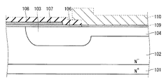
図9は、本発明の前提技術としての、トレンチゲート構造をもつパワーMOSFETのトレンチ終端領域の上面図である。便宜上、ゲート電極107、ソース電極110は一部分を示し、またN+ソース領域は図示を省略している。
図1は、本発明にかかる半導体装置である、トレンチゲート構造をもつパワーMOSFETのトレンチ終端領域の上面図である。便宜上、ゲート電極7とソース電極11は一部分を示し、またN+ソース領域は図示を省略している。
ここで、ゲート絶縁耐量を測定する場合には、ソースとドレインを短絡した状態で、ゲート−ソース間に電圧(Vg)を印加し、電流(Ig)を計測する。また、ドレイン−ソース間の耐圧を測定する場合には、ゲートとソースを短絡した状態で、ドレインに電圧(Vd)を印加し、ドレイン電流(Id)を計測する。このときのドレイン電流をもれ電流とも呼ぶ。
本発明にかかる実施の形態1によれば、半導体装置において、Pベース層4表面からPウェル層3表面へ跨って延在して形成され、Pウェル層3表面に延在方向のトレンチ端部8を有するトレンチ5を備え、トレンチ5は、トレンチ端部8からPベース層4・Pウェル層3境界近傍のPベース層4表面内に跨って延在する第1領域と、Pベース層4表面内において第1領域端部から延在する第2領域とを備え、第1領域は、第2領域よりもそのトレンチ幅が広いことで、トレンチ端部8に尖端形状が形成されることを抑制し、ゲート酸化膜耐量低下や耐圧発振を防止することが可能となる。
Claims (4)
- 第1導電型の半導体基板上に形成された、第1導電型のドリフト層と、
前記ドリフト層表面に選択的に形成された、第2導電型のベース層と、
前記ベース層と隣接して前記ドリフト層表面に形成された、第2導電型のウェル層と、
前記ベース層表面から前記ウェル層表面へ跨って延在して形成され、前記ウェル層表面に延在方向のトレンチ端部を有するトレンチと、
前記トレンチを含む前記ドリフト層上に、選択的に形成されたゲート電極とを備え、
前記トレンチは、前記トレンチ端部から前記ベース層・前記ウェル層境界近傍の前記ベース層表面内に跨って延在する第1領域と、前記ベース層表面内において前記第1領域端部から延在する第2領域とを備え、
前記第1領域は、前記第2領域よりもそのトレンチ幅が広い、
半導体装置。 - 前記第2領域のトレンチ幅は、0.25μm以下である、
請求項1に記載の半導体装置。 - 前記第1領域のトレンチ幅は、0.35μm以上である、
請求項1または2に記載の半導体装置。 - 前記半導体基板は、ワイドバンドギャップ半導体からなる、
請求項1〜3のいずれかに記載の半導体装置。
Priority Applications (5)
| Application Number | Priority Date | Filing Date | Title |
|---|---|---|---|
| JP2010281547A JP5656608B2 (ja) | 2010-12-17 | 2010-12-17 | 半導体装置 |
| US13/205,085 US8530966B2 (en) | 2010-12-17 | 2011-08-08 | Semiconductor device |
| CN201110276618.7A CN102544071B (zh) | 2010-12-17 | 2011-09-05 | 半导体装置 |
| DE102011086733.3A DE102011086733B4 (de) | 2010-12-17 | 2011-11-21 | Halbleitervorrichtung |
| KR1020110130027A KR101319470B1 (ko) | 2010-12-17 | 2011-12-07 | 반도체 장치 |
Applications Claiming Priority (1)
| Application Number | Priority Date | Filing Date | Title |
|---|---|---|---|
| JP2010281547A JP5656608B2 (ja) | 2010-12-17 | 2010-12-17 | 半導体装置 |
Publications (2)
| Publication Number | Publication Date |
|---|---|
| JP2012129446A JP2012129446A (ja) | 2012-07-05 |
| JP5656608B2 true JP5656608B2 (ja) | 2015-01-21 |
Family
ID=46233261
Family Applications (1)
| Application Number | Title | Priority Date | Filing Date |
|---|---|---|---|
| JP2010281547A Active JP5656608B2 (ja) | 2010-12-17 | 2010-12-17 | 半導体装置 |
Country Status (5)
| Country | Link |
|---|---|
| US (1) | US8530966B2 (ja) |
| JP (1) | JP5656608B2 (ja) |
| KR (1) | KR101319470B1 (ja) |
| CN (1) | CN102544071B (ja) |
| DE (1) | DE102011086733B4 (ja) |
Families Citing this family (9)
| Publication number | Priority date | Publication date | Assignee | Title |
|---|---|---|---|---|
| KR101422953B1 (ko) | 2012-12-14 | 2014-08-13 | 삼성전기주식회사 | 전력 반도체 소자 및 그 제조 방법 |
| KR101452091B1 (ko) | 2013-02-26 | 2014-10-16 | 삼성전기주식회사 | 전력 반도체 소자 및 그 제조 방법 |
| JP6020317B2 (ja) * | 2013-04-05 | 2016-11-02 | 三菱電機株式会社 | 半導体素子 |
| DE112014006788B4 (de) * | 2014-10-29 | 2022-05-12 | Hitachi, Ltd. | Halbleiterbauelement, Leistungsmodul und Leistungswandler |
| JP6600475B2 (ja) | 2015-03-27 | 2019-10-30 | ローム株式会社 | 半導体装置 |
| JP2018074126A (ja) * | 2016-11-04 | 2018-05-10 | トヨタ自動車株式会社 | 半導体装置 |
| JP6632513B2 (ja) * | 2016-12-07 | 2020-01-22 | 株式会社東芝 | 半導体装置及びその製造方法 |
| JP6967907B2 (ja) | 2017-08-07 | 2021-11-17 | ルネサスエレクトロニクス株式会社 | 半導体装置及び半導体装置の製造方法 |
| JP6876767B2 (ja) * | 2019-10-07 | 2021-05-26 | ローム株式会社 | 半導体装置 |
Family Cites Families (13)
| Publication number | Priority date | Publication date | Assignee | Title |
|---|---|---|---|---|
| JP3904648B2 (ja) | 1997-01-31 | 2007-04-11 | 株式会社ルネサステクノロジ | 半導体装置 |
| US6303410B1 (en) * | 1998-06-01 | 2001-10-16 | North Carolina State University | Methods of forming power semiconductor devices having T-shaped gate electrodes |
| GB0012138D0 (en) * | 2000-05-20 | 2000-07-12 | Koninkl Philips Electronics Nv | A semiconductor device |
| US7576388B1 (en) * | 2002-10-03 | 2009-08-18 | Fairchild Semiconductor Corporation | Trench-gate LDMOS structures |
| JP3931138B2 (ja) * | 2002-12-25 | 2007-06-13 | 三菱電機株式会社 | 電力用半導体装置及び電力用半導体装置の製造方法 |
| US7560359B2 (en) * | 2004-11-26 | 2009-07-14 | Samsung Electronics Co., Ltd. | Methods of forming asymmetric recesses and gate structures that fill such recesses and related methods of forming semiconductor devices that include such recesses and gate structures |
| JP2006229135A (ja) * | 2005-02-21 | 2006-08-31 | Denso Corp | 半導体装置の製造方法 |
| US7276766B2 (en) * | 2005-08-01 | 2007-10-02 | Semiconductor Components Industries, L.L.C. | Semiconductor structure with improved on resistance and breakdown voltage performance |
| JP2007048769A (ja) * | 2005-08-05 | 2007-02-22 | Matsushita Electric Ind Co Ltd | 半導体装置およびその製造方法 |
| JP2005322949A (ja) | 2005-08-05 | 2005-11-17 | Renesas Technology Corp | 半導体装置 |
| US7667265B2 (en) * | 2006-01-30 | 2010-02-23 | Fairchild Semiconductor Corporation | Varying mesa dimensions in high cell density trench MOSFET |
| KR100809332B1 (ko) | 2006-09-04 | 2008-03-05 | 삼성전자주식회사 | 반도체 집적 회로 장치 및 그 제조 방법 |
| JP2009188294A (ja) * | 2008-02-08 | 2009-08-20 | Nec Electronics Corp | パワーmosfet |
-
2010
- 2010-12-17 JP JP2010281547A patent/JP5656608B2/ja active Active
-
2011
- 2011-08-08 US US13/205,085 patent/US8530966B2/en active Active
- 2011-09-05 CN CN201110276618.7A patent/CN102544071B/zh active Active
- 2011-11-21 DE DE102011086733.3A patent/DE102011086733B4/de active Active
- 2011-12-07 KR KR1020110130027A patent/KR101319470B1/ko active IP Right Grant
Also Published As
| Publication number | Publication date |
|---|---|
| DE102011086733B4 (de) | 2020-03-26 |
| US20120153382A1 (en) | 2012-06-21 |
| CN102544071A (zh) | 2012-07-04 |
| US8530966B2 (en) | 2013-09-10 |
| KR101319470B1 (ko) | 2013-10-17 |
| KR20120068701A (ko) | 2012-06-27 |
| CN102544071B (zh) | 2014-11-05 |
| DE102011086733A1 (de) | 2012-06-21 |
| JP2012129446A (ja) | 2012-07-05 |
Similar Documents
| Publication | Publication Date | Title |
|---|---|---|
| JP5656608B2 (ja) | 半導体装置 | |
| CN105280711B (zh) | 电荷补偿结构及用于其的制造 | |
| US10672878B2 (en) | Silicon carbide semiconductor device | |
| JP2009038318A (ja) | 半導体装置 | |
| JP6183550B2 (ja) | 半導体装置 | |
| JP2013152981A (ja) | 半導体装置及びその製造方法 | |
| JP2012064849A (ja) | 半導体装置 | |
| JP2013065749A (ja) | 半導体装置 | |
| JP2008091373A (ja) | 電力用半導体装置 | |
| JP2020025050A (ja) | 半導体装置 | |
| JP2010251404A (ja) | 半導体装置 | |
| KR20120005712U (ko) | 쇼트키 다이오드의 종단 영역 트렌치 구조 | |
| TWI629785B (zh) | 高電壓積體電路的高電壓終端結構 | |
| US9111766B2 (en) | Transistor device with a field electrode | |
| JP5957171B2 (ja) | 半導体装置及びその製造方法 | |
| JP7345354B2 (ja) | 半導体装置 | |
| JP2019145646A (ja) | 半導体装置 | |
| KR101616157B1 (ko) | 전력 반도체 소자 및 그 제조 방법 | |
| JP7330396B2 (ja) | 半導体装置及び電力変換装置 | |
| KR20140067445A (ko) | 전력 반도체 소자 | |
| JP7334678B2 (ja) | 半導体装置 | |
| JP7321820B2 (ja) | 半導体装置、インバータ回路、駆動装置、車両、及び、昇降機 | |
| TWM449354U (zh) | 功率半導體元件及其邊緣終端結構 | |
| US20230326972A1 (en) | Silicon carbide semiconductor power transistor and method of manufacturing the same | |
| JP2007134421A (ja) | パワーmosfet、igbtなどの縦型半導体装置とその製造方法 |
Legal Events
| Date | Code | Title | Description |
|---|---|---|---|
| A621 | Written request for application examination |
Free format text: JAPANESE INTERMEDIATE CODE: A621 Effective date: 20130325 |
|
| A977 | Report on retrieval |
Free format text: JAPANESE INTERMEDIATE CODE: A971007 Effective date: 20140313 |
|
| A131 | Notification of reasons for refusal |
Free format text: JAPANESE INTERMEDIATE CODE: A131 Effective date: 20140401 |
|
| TRDD | Decision of grant or rejection written | ||
| A01 | Written decision to grant a patent or to grant a registration (utility model) |
Free format text: JAPANESE INTERMEDIATE CODE: A01 Effective date: 20141028 |
|
| A61 | First payment of annual fees (during grant procedure) |
Free format text: JAPANESE INTERMEDIATE CODE: A61 Effective date: 20141125 |
|
| R150 | Certificate of patent or registration of utility model |
Ref document number: 5656608 Country of ref document: JP Free format text: JAPANESE INTERMEDIATE CODE: R150 |
|
| R250 | Receipt of annual fees |
Free format text: JAPANESE INTERMEDIATE CODE: R250 |
|
| R250 | Receipt of annual fees |
Free format text: JAPANESE INTERMEDIATE CODE: R250 |
|
| R250 | Receipt of annual fees |
Free format text: JAPANESE INTERMEDIATE CODE: R250 |
|
| R250 | Receipt of annual fees |
Free format text: JAPANESE INTERMEDIATE CODE: R250 |
|
| R250 | Receipt of annual fees |
Free format text: JAPANESE INTERMEDIATE CODE: R250 |
|
| R250 | Receipt of annual fees |
Free format text: JAPANESE INTERMEDIATE CODE: R250 |
|
| R250 | Receipt of annual fees |
Free format text: JAPANESE INTERMEDIATE CODE: R250 |