JP5445006B2 - 基板処理装置、基板処理方法及び記憶媒体 - Google Patents
基板処理装置、基板処理方法及び記憶媒体 Download PDFInfo
- Publication number
- JP5445006B2 JP5445006B2 JP2009231969A JP2009231969A JP5445006B2 JP 5445006 B2 JP5445006 B2 JP 5445006B2 JP 2009231969 A JP2009231969 A JP 2009231969A JP 2009231969 A JP2009231969 A JP 2009231969A JP 5445006 B2 JP5445006 B2 JP 5445006B2
- Authority
- JP
- Japan
- Prior art keywords
- priority
- processing
- substrate
- unit
- wafer
- Prior art date
- Legal status (The legal status is an assumption and is not a legal conclusion. Google has not performed a legal analysis and makes no representation as to the accuracy of the status listed.)
- Active
Links
- 238000012545 processing Methods 0.000 title claims description 503
- 239000000758 substrate Substances 0.000 title claims description 130
- 238000003860 storage Methods 0.000 title claims description 14
- 238000003672 processing method Methods 0.000 title description 2
- 230000007246 mechanism Effects 0.000 claims description 24
- 239000007788 liquid Substances 0.000 description 244
- 235000012431 wafers Nutrition 0.000 description 202
- 238000000034 method Methods 0.000 description 41
- 238000012546 transfer Methods 0.000 description 30
- 239000000126 substance Substances 0.000 description 28
- 239000000243 solution Substances 0.000 description 17
- XLYOFNOQVPJJNP-UHFFFAOYSA-N water Substances O XLYOFNOQVPJJNP-UHFFFAOYSA-N 0.000 description 10
- 238000004140 cleaning Methods 0.000 description 8
- 239000008367 deionised water Substances 0.000 description 7
- 229910021641 deionized water Inorganic materials 0.000 description 7
- KRHYYFGTRYWZRS-UHFFFAOYSA-N Fluorane Chemical compound F KRHYYFGTRYWZRS-UHFFFAOYSA-N 0.000 description 4
- 238000010586 diagram Methods 0.000 description 4
- 238000001035 drying Methods 0.000 description 4
- FFUAGWLWBBFQJT-UHFFFAOYSA-N hexamethyldisilazane Chemical compound C[Si](C)(C)N[Si](C)(C)C FFUAGWLWBBFQJT-UHFFFAOYSA-N 0.000 description 4
- 239000000356 contaminant Substances 0.000 description 3
- 239000002245 particle Substances 0.000 description 3
- 239000004065 semiconductor Substances 0.000 description 3
- 238000011144 upstream manufacturing Methods 0.000 description 3
- QGZKDVFQNNGYKY-UHFFFAOYSA-N Ammonia Chemical compound N QGZKDVFQNNGYKY-UHFFFAOYSA-N 0.000 description 2
- VEXZGXHMUGYJMC-UHFFFAOYSA-N Hydrochloric acid Chemical compound Cl VEXZGXHMUGYJMC-UHFFFAOYSA-N 0.000 description 2
- MHAJPDPJQMAIIY-UHFFFAOYSA-N Hydrogen peroxide Chemical compound OO MHAJPDPJQMAIIY-UHFFFAOYSA-N 0.000 description 2
- 230000002378 acidificating effect Effects 0.000 description 2
- 230000001174 ascending effect Effects 0.000 description 2
- 230000003028 elevating effect Effects 0.000 description 2
- 239000012530 fluid Substances 0.000 description 2
- 238000004519 manufacturing process Methods 0.000 description 2
- 238000005192 partition Methods 0.000 description 2
- 230000007723 transport mechanism Effects 0.000 description 2
- 229910021529 ammonia Inorganic materials 0.000 description 1
- 239000007864 aqueous solution Substances 0.000 description 1
- 238000012993 chemical processing Methods 0.000 description 1
- 238000004891 communication Methods 0.000 description 1
- 238000007796 conventional method Methods 0.000 description 1
- 230000003247 decreasing effect Effects 0.000 description 1
- 230000002950 deficient Effects 0.000 description 1
- 230000003111 delayed effect Effects 0.000 description 1
- 238000007599 discharging Methods 0.000 description 1
- 230000000694 effects Effects 0.000 description 1
- 239000007888 film coating Substances 0.000 description 1
- 238000009501 film coating Methods 0.000 description 1
- 239000012535 impurity Substances 0.000 description 1
- 239000008155 medical solution Substances 0.000 description 1
- 239000002184 metal Substances 0.000 description 1
- 230000003287 optical effect Effects 0.000 description 1
- 238000012360 testing method Methods 0.000 description 1
- 239000002351 wastewater Substances 0.000 description 1
Images


Classifications
-
- H—ELECTRICITY
- H01—ELECTRIC ELEMENTS
- H01L—SEMICONDUCTOR DEVICES NOT COVERED BY CLASS H10
- H01L21/00—Processes or apparatus adapted for the manufacture or treatment of semiconductor or solid state devices or of parts thereof
- H01L21/67—Apparatus specially adapted for handling semiconductor or electric solid state devices during manufacture or treatment thereof; Apparatus specially adapted for handling wafers during manufacture or treatment of semiconductor or electric solid state devices or components ; Apparatus not specifically provided for elsewhere
- H01L21/677—Apparatus specially adapted for handling semiconductor or electric solid state devices during manufacture or treatment thereof; Apparatus specially adapted for handling wafers during manufacture or treatment of semiconductor or electric solid state devices or components ; Apparatus not specifically provided for elsewhere for conveying, e.g. between different workstations
- H01L21/67739—Apparatus specially adapted for handling semiconductor or electric solid state devices during manufacture or treatment thereof; Apparatus specially adapted for handling wafers during manufacture or treatment of semiconductor or electric solid state devices or components ; Apparatus not specifically provided for elsewhere for conveying, e.g. between different workstations into and out of processing chamber
-
- G—PHYSICS
- G05—CONTROLLING; REGULATING
- G05B—CONTROL OR REGULATING SYSTEMS IN GENERAL; FUNCTIONAL ELEMENTS OF SUCH SYSTEMS; MONITORING OR TESTING ARRANGEMENTS FOR SUCH SYSTEMS OR ELEMENTS
- G05B19/00—Programme-control systems
- G05B19/02—Programme-control systems electric
- G05B19/418—Total factory control, i.e. centrally controlling a plurality of machines, e.g. direct or distributed numerical control [DNC], flexible manufacturing systems [FMS], integrated manufacturing systems [IMS], computer integrated manufacturing [CIM]
- G05B19/41815—Total factory control, i.e. centrally controlling a plurality of machines, e.g. direct or distributed numerical control [DNC], flexible manufacturing systems [FMS], integrated manufacturing systems [IMS], computer integrated manufacturing [CIM] characterised by the cooperation between machine tools, manipulators and conveyor or other workpiece supply system, workcell
-
- G—PHYSICS
- G05—CONTROLLING; REGULATING
- G05B—CONTROL OR REGULATING SYSTEMS IN GENERAL; FUNCTIONAL ELEMENTS OF SUCH SYSTEMS; MONITORING OR TESTING ARRANGEMENTS FOR SUCH SYSTEMS OR ELEMENTS
- G05B19/00—Programme-control systems
- G05B19/02—Programme-control systems electric
- G05B19/418—Total factory control, i.e. centrally controlling a plurality of machines, e.g. direct or distributed numerical control [DNC], flexible manufacturing systems [FMS], integrated manufacturing systems [IMS], computer integrated manufacturing [CIM]
- G05B19/4189—Total factory control, i.e. centrally controlling a plurality of machines, e.g. direct or distributed numerical control [DNC], flexible manufacturing systems [FMS], integrated manufacturing systems [IMS], computer integrated manufacturing [CIM] characterised by the transport system
-
- H—ELECTRICITY
- H01—ELECTRIC ELEMENTS
- H01L—SEMICONDUCTOR DEVICES NOT COVERED BY CLASS H10
- H01L21/00—Processes or apparatus adapted for the manufacture or treatment of semiconductor or solid state devices or of parts thereof
- H01L21/67—Apparatus specially adapted for handling semiconductor or electric solid state devices during manufacture or treatment thereof; Apparatus specially adapted for handling wafers during manufacture or treatment of semiconductor or electric solid state devices or components ; Apparatus not specifically provided for elsewhere
- H01L21/67005—Apparatus not specifically provided for elsewhere
- H01L21/67242—Apparatus for monitoring, sorting or marking
- H01L21/67276—Production flow monitoring, e.g. for increasing throughput
-
- G—PHYSICS
- G05—CONTROLLING; REGULATING
- G05B—CONTROL OR REGULATING SYSTEMS IN GENERAL; FUNCTIONAL ELEMENTS OF SUCH SYSTEMS; MONITORING OR TESTING ARRANGEMENTS FOR SUCH SYSTEMS OR ELEMENTS
- G05B2219/00—Program-control systems
- G05B2219/30—Nc systems
- G05B2219/31—From computer integrated manufacturing till monitoring
- G05B2219/31002—Computer controlled agv conveys workpieces between buffer and cell
-
- G—PHYSICS
- G05—CONTROLLING; REGULATING
- G05B—CONTROL OR REGULATING SYSTEMS IN GENERAL; FUNCTIONAL ELEMENTS OF SUCH SYSTEMS; MONITORING OR TESTING ARRANGEMENTS FOR SUCH SYSTEMS OR ELEMENTS
- G05B2219/00—Program-control systems
- G05B2219/30—Nc systems
- G05B2219/45—Nc applications
- G05B2219/45031—Manufacturing semiconductor wafers
Landscapes
- Engineering & Computer Science (AREA)
- Manufacturing & Machinery (AREA)
- Physics & Mathematics (AREA)
- General Physics & Mathematics (AREA)
- Automation & Control Theory (AREA)
- Computer Hardware Design (AREA)
- Condensed Matter Physics & Semiconductors (AREA)
- Microelectronics & Electronic Packaging (AREA)
- Power Engineering (AREA)
- General Engineering & Computer Science (AREA)
- Quality & Reliability (AREA)
- Container, Conveyance, Adherence, Positioning, Of Wafer (AREA)
- Cleaning Or Drying Semiconductors (AREA)
Description
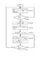
この基板搬入ブロックから搬入された基板に対して同種の処理を行うため複数の処理ユニットと、前記基板搬入ブロックと各処理ユニットとの間で基板を搬送する基板搬送部とを含む処理ブロックと、
他の基板よりも処理を優先する優先基板が基板搬送容器により前記容器載置部に搬送されたときに、前記複数の処理ユニットの一部が割り振られた優先処理ユニットのうち、次の基板の搬入が可能になった優先処理ユニットに、他の基板に優先して優先基板を搬入して処理を行うと共に、前記優先処理ユニット以外の処理ユニットでは、前記他の基板を搬入して処理を並行して行うように制御信号を出力する制御部と、
前記優先基板の処理の優先度と優先処理ユニットの数とを対応付けるためのデータを記憶する記憶部と、を備え、
前記優先処理ユニットの割り振りは、前記容器載置部に優先基板を含む基板搬送容器が載置された後に行われ、
優先基板には前記優先度が割り当てられ、
前記制御部は、基板搬送容器内の優先基板の優先度に応じて優先処理ユニットの数を変更することを特徴とする。
ここで、前記優先処理ユニットの数は、優先基板の枚数に応じて変更されてもよい。
この基板搬入ブロックから搬入された基板に対して同種の処理を行うため複数の処理ユニットと、前記基板搬入ブロックと各処理ユニットとの間で基板を搬送する基板搬送部とを含む処理ブロックと、
他の基板よりも処理を優先する優先基板が基板搬送容器により前記容器載置部に搬送されたときに、前記複数の処理ユニットの一部が割り振られた優先処理ユニットのうち、次の基板の搬入が可能になった優先処理ユニットに、他の基板に優先して優先基板を搬入して処理を行うと共に、前記優先処理ユニット以外の処理ユニットでは、前記他の基板を搬入して処理を並行して行うように制御信号を出力する制御部と、を備え、
前記優先処理ユニットの割り振りは、前記容器載置部に優先基板を含む基板搬送容器が載置された後に行われ、
優先基板には処理に許容される許容処理時間が決められ、
前記制御部は、優先基板の許容処理時間を取得し、実際の処理時間が前記許容処理時間に近くなるように、優先処理ユニットの台数に対応させて記憶した優先基板の推定処理時間に基づいて優先処理ユニットに割り振る処理ユニットの数を決定することを特徴とする。
上記基板処理装置は、以下の特徴を備えていてもよい。
(a)前記優先処理ユニットの数は、優先基板の枚数に応じて変更されること。
(b)前記優先基板の処理の優先度と優先処理ユニットの数とを対応付けるためのデータを記憶する記憶部を有し、優先基板には前記優先度が割り当てられ、前記制御部は、基板搬送容器内の優先基板の優先度に応じて優先処理ユニットの数を変更すること。
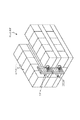
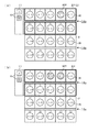
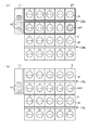
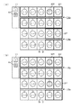
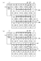
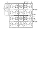
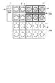
以上に説明したFOUP載置部11、搬送部12、受け渡し部13は、本実施の形態の基板搬入ブロックを構成している。
さらには、上述の液処理装置1においては、各々10台の液処理ユニット2を備える液処理ブロック14a、14bが上下に2段積み重ねられた例を用いて説明したが、各液処理ブロック14a、14bに設けられる液処理ユニット2の台数、液処理ブロック14a、14bの数を適宜増減してもよいことは勿論である。
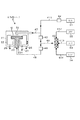
WP 優先ウエハ
1 液処理装置
11 FOUP載置部
12 搬送部
121 搬入出アーム
13 受け渡し部
14a、14b
液処理ブロック
141a、141b
プロセスアーム
2 液処理ユニット
2P 優先処理ユニット
5 制御部
Claims (5)
- 基板を収納した複数の基板搬送容器を載置可能な容器載置部と、この容器載置部に載置された基板搬送容器に対して基板の受け渡しを行う受け渡し機構と、を含む基板搬入ブロックと、
この基板搬入ブロックから搬入された基板に対して同種の処理を行うため複数の処理ユニットと、前記基板搬入ブロックと各処理ユニットとの間で基板を搬送する基板搬送部とを含む処理ブロックと、
他の基板よりも処理を優先する優先基板が基板搬送容器により前記容器載置部に搬送されたときに、前記複数の処理ユニットの一部が割り振られた優先処理ユニットのうち、次の基板の搬入が可能になった優先処理ユニットに、他の基板に優先して優先基板を搬入して処理を行うと共に、前記優先処理ユニット以外の処理ユニットでは、前記他の基板を搬入して処理を並行して行うように制御信号を出力する制御部と、
前記優先基板の処理の優先度と優先処理ユニットの数とを対応付けるためのデータを記憶する記憶部と、を備え、
前記優先処理ユニットの割り振りは、前記容器載置部に優先基板を含む基板搬送容器が載置された後に行われ、
優先基板には前記優先度が割り当てられ、
前記制御部は、基板搬送容器内の優先基板の優先度に応じて優先処理ユニットの数を変更することを特徴とする基板処理装置。 - 前記優先処理ユニットの数は、優先基板の枚数に応じて変更されることを特徴とする請求項1に記載の基板処理装置。
- 基板を収納した複数の基板搬送容器を載置可能な容器載置部と、この容器載置部に載置された基板搬送容器に対して基板の受け渡しを行う受け渡し機構と、を含む基板搬入ブロックと、
この基板搬入ブロックから搬入された基板に対して同種の処理を行うため複数の処理ユニットと、前記基板搬入ブロックと各処理ユニットとの間で基板を搬送する基板搬送部とを含む処理ブロックと、
他の基板よりも処理を優先する優先基板が基板搬送容器により前記容器載置部に搬送されたときに、前記複数の処理ユニットの一部が割り振られた優先処理ユニットのうち、次の基板の搬入が可能になった優先処理ユニットに、他の基板に優先して優先基板を搬入して処理を行うと共に、前記優先処理ユニット以外の処理ユニットでは、前記他の基板を搬入して処理を並行して行うように制御信号を出力する制御部と、を備え、
前記優先処理ユニットの割り振りは、前記容器載置部に優先基板を含む基板搬送容器が載置された後に行われ、
優先基板には処理に許容される許容処理時間が決められ、
前記制御部は、優先基板の許容処理時間を取得し、実際の処理時間が前記許容処理時間に近くなるように、優先処理ユニットの台数に対応させて記憶した優先基板の推定処理時間に基づいて優先処理ユニットに割り振る処理ユニットの数を決定することを特徴とする基板処理装置。 - 前記優先処理ユニットの数は、優先基板の枚数に応じて変更されることを特徴とする請求項3に記載の基板処理装置。
- 前記優先基板の処理の優先度と優先処理ユニットの数とを対応付けるためのデータを記憶する記憶部を有し、
優先基板には前記優先度が割り当てられ、
前記制御部は、基板搬送容器内の優先基板の優先度に応じて優先処理ユニットの数を変更することを特徴とする請求項3または4に記載の基板処理装置。
Priority Applications (3)
| Application Number | Priority Date | Filing Date | Title |
|---|---|---|---|
| JP2009231969A JP5445006B2 (ja) | 2009-10-05 | 2009-10-05 | 基板処理装置、基板処理方法及び記憶媒体 |
| US12/896,236 US8447422B2 (en) | 2009-10-05 | 2010-10-01 | Substrate processing apparatus, substrate processing method, and storage medium |
| KR1020100096958A KR101449782B1 (ko) | 2009-10-05 | 2010-10-05 | 기판 처리 장치, 기판 처리 방법 및 기억 매체 |
Applications Claiming Priority (1)
| Application Number | Priority Date | Filing Date | Title |
|---|---|---|---|
| JP2009231969A JP5445006B2 (ja) | 2009-10-05 | 2009-10-05 | 基板処理装置、基板処理方法及び記憶媒体 |
Publications (3)
| Publication Number | Publication Date |
|---|---|
| JP2011082276A JP2011082276A (ja) | 2011-04-21 |
| JP2011082276A5 JP2011082276A5 (ja) | 2012-02-23 |
| JP5445006B2 true JP5445006B2 (ja) | 2014-03-19 |
Family
ID=43823822
Family Applications (1)
| Application Number | Title | Priority Date | Filing Date |
|---|---|---|---|
| JP2009231969A Active JP5445006B2 (ja) | 2009-10-05 | 2009-10-05 | 基板処理装置、基板処理方法及び記憶媒体 |
Country Status (3)
| Country | Link |
|---|---|
| US (1) | US8447422B2 (ja) |
| JP (1) | JP5445006B2 (ja) |
| KR (1) | KR101449782B1 (ja) |
Cited By (1)
| Publication number | Priority date | Publication date | Assignee | Title |
|---|---|---|---|---|
| US11809158B2 (en) | 2018-07-23 | 2023-11-07 | Semes Co., Ltd. | Apparatus and method for treating substrate based on defect values of transfer paths |
Families Citing this family (15)
| Publication number | Priority date | Publication date | Assignee | Title |
|---|---|---|---|---|
| JP5006122B2 (ja) | 2007-06-29 | 2012-08-22 | 株式会社Sokudo | 基板処理装置 |
| JP5128918B2 (ja) | 2007-11-30 | 2013-01-23 | 株式会社Sokudo | 基板処理装置 |
| JP5001828B2 (ja) | 2007-12-28 | 2012-08-15 | 株式会社Sokudo | 基板処理装置 |
| JP5179170B2 (ja) | 2007-12-28 | 2013-04-10 | 株式会社Sokudo | 基板処理装置 |
| JP5847515B2 (ja) * | 2011-09-27 | 2016-01-20 | 株式会社Screenホールディングス | 基板処理装置のためのスケジュール作成方法およびスケジュール作成プログラム |
| KR101909099B1 (ko) * | 2011-10-13 | 2018-10-17 | 세메스 주식회사 | 웨이퍼 처리 방법 |
| JP6045946B2 (ja) * | 2012-07-13 | 2016-12-14 | 株式会社Screenホールディングス | 基板処理装置、プログラムおよび記録媒体 |
| JP5981307B2 (ja) * | 2012-11-07 | 2016-08-31 | 東京エレクトロン株式会社 | 処理方法及び処理装置 |
| JP5977728B2 (ja) * | 2013-11-14 | 2016-08-24 | 東京エレクトロン株式会社 | 基板処理システム |
| US10236196B2 (en) * | 2013-11-14 | 2019-03-19 | Tokyo Electron Limited | Substrate processing system |
| JP6297001B2 (ja) * | 2014-03-19 | 2018-03-20 | キヤノン株式会社 | リソグラフィ装置、リソグラフィ方法、リソグラフィシステム、プログラム、および物品の製造方法 |
| US10520932B2 (en) * | 2014-07-03 | 2019-12-31 | Taiwan Semiconductor Manufacturing Co., Ltd | Transport system and method |
| JP6324246B2 (ja) * | 2014-07-11 | 2018-05-16 | キヤノン株式会社 | リソグラフィ装置、および物品製造方法 |
| JP6552931B2 (ja) * | 2015-09-18 | 2019-07-31 | 東京エレクトロン株式会社 | 基板処理装置及び基板処理方法 |
| KR20200072060A (ko) | 2018-12-12 | 2020-06-22 | 세메스 주식회사 | 기판 처리 장치 및 방법 |
Family Cites Families (37)
| Publication number | Priority date | Publication date | Assignee | Title |
|---|---|---|---|---|
| JP2918464B2 (ja) | 1994-04-08 | 1999-07-12 | 大日本スクリーン製造株式会社 | 基板処理装置 |
| US5687085A (en) * | 1994-04-08 | 1997-11-11 | Dainippon Screen Mfg. Co., Ltd. | Substrate processing apparatus and method |
| US5928389A (en) * | 1996-10-21 | 1999-07-27 | Applied Materials, Inc. | Method and apparatus for priority based scheduling of wafer processing within a multiple chamber semiconductor wafer processing tool |
| KR100646906B1 (ko) * | 1998-09-22 | 2006-11-17 | 동경 엘렉트론 주식회사 | 기판처리장치 및 기판처리방법 |
| US6662076B1 (en) * | 1999-02-10 | 2003-12-09 | Advanced Micro Devices, Inc. | Management of move requests from a factory system to an automated material handling system |
| JP3515724B2 (ja) * | 2000-01-13 | 2004-04-05 | Necエレクトロニクス株式会社 | 製品の製造管理方法及び製造管理システム |
| EP1124252A2 (en) * | 2000-02-10 | 2001-08-16 | Applied Materials, Inc. | Apparatus and process for processing substrates |
| TW495819B (en) * | 2000-05-31 | 2002-07-21 | Toshiba Corp | Method and system for electronic commerce of semiconductor product, system and method of production, and design system, design method and manufacturing method of production equipment |
| JP2001351848A (ja) * | 2000-06-07 | 2001-12-21 | Tokyo Electron Ltd | 基板処理システム及び基板処理方法 |
| JP2002313880A (ja) * | 2001-04-19 | 2002-10-25 | Hitachi Ltd | 半導体集積回路装置の製造方法 |
| US6564113B1 (en) * | 2001-06-15 | 2003-05-13 | Advanced Micro Devices, Inc. | Lot start agent that calculates virtual WIP time in a multi-product and multi-bottleneck manufacturing environment |
| US6580967B2 (en) * | 2001-06-26 | 2003-06-17 | Applied Materials, Inc. | Method for providing distributed material management and flow control in an integrated circuit factory |
| US6763277B1 (en) * | 2001-07-16 | 2004-07-13 | Advanced Micro Devices, Inc. | Method and apparatus for proactive dispatch system to improve line balancing |
| JP2003173204A (ja) * | 2001-12-07 | 2003-06-20 | Mitsubishi Electric Corp | 処理装置への割り付け方法 |
| JP2004087675A (ja) * | 2002-08-26 | 2004-03-18 | Dainippon Screen Mfg Co Ltd | 基板処理装置 |
| US7778721B2 (en) * | 2003-01-27 | 2010-08-17 | Applied Materials, Inc. | Small lot size lithography bays |
| US7221993B2 (en) * | 2003-01-27 | 2007-05-22 | Applied Materials, Inc. | Systems and methods for transferring small lot size substrate carriers between processing tools |
| US7720557B2 (en) * | 2003-11-06 | 2010-05-18 | Applied Materials, Inc. | Methods and apparatus for enhanced operation of substrate carrier handlers |
| US20070276531A1 (en) * | 2003-11-06 | 2007-11-29 | Applied Materials, Inc. | Methods and apparatus for enhanced operation of substrate carrier handlers |
| JP4030509B2 (ja) * | 2004-02-13 | 2008-01-09 | 株式会社日立製作所 | 真空処理方法及び真空処理装置 |
| US7177716B2 (en) * | 2004-02-28 | 2007-02-13 | Applied Materials, Inc. | Methods and apparatus for material control system interface |
| JP4477982B2 (ja) * | 2004-10-08 | 2010-06-09 | 東京エレクトロン株式会社 | クラスタツールの処理システム及び滞在時間監視プログラム |
| US7651306B2 (en) * | 2004-12-22 | 2010-01-26 | Applied Materials, Inc. | Cartesian robot cluster tool architecture |
| US7798764B2 (en) * | 2005-12-22 | 2010-09-21 | Applied Materials, Inc. | Substrate processing sequence in a cartesian robot cluster tool |
| US20060182535A1 (en) * | 2004-12-22 | 2006-08-17 | Mike Rice | Cartesian robot design |
| US7371022B2 (en) * | 2004-12-22 | 2008-05-13 | Sokudo Co., Ltd. | Developer endpoint detection in a track lithography system |
| US20060241813A1 (en) * | 2005-04-22 | 2006-10-26 | Applied Materials, Inc. | Optimized cluster tool transfer process and collision avoidance design |
| JP4681356B2 (ja) * | 2005-06-13 | 2011-05-11 | 株式会社日立ハイテクノロジーズ | 欠陥自動観察分類システム、欠陥自動観察分類システムにおける装置の選択方法、プログラム、及び観察装置 |
| US7780392B2 (en) * | 2005-10-27 | 2010-08-24 | Muratec Automation Co., Ltd. | Horizontal array stocker |
| US20070250202A1 (en) * | 2006-04-17 | 2007-10-25 | Tokyo Electron Limited | Coating and developing system, method of controlling coating and developing system and storage medium |
| DE102006025406A1 (de) * | 2006-05-31 | 2007-12-06 | Advanced Micro Devices, Inc., Sunnyvale | Verfahren und System zum Steuern von Prozessanlagen durch Unterbrechen von Prozessaufgaben in Abhängigkeit von der Aufgabenpriorität |
| JP4767783B2 (ja) | 2006-07-26 | 2011-09-07 | 東京エレクトロン株式会社 | 液処理装置 |
| JP2008078630A (ja) * | 2006-08-24 | 2008-04-03 | Hitachi Kokusai Electric Inc | 基板処理システム |
| JP2008192866A (ja) * | 2007-02-06 | 2008-08-21 | Hitachi Kokusai Electric Inc | 基板処理装置 |
| US8070410B2 (en) * | 2008-02-05 | 2011-12-06 | Lutz Rebstock | Scalable stocker with automatic handling buffer |
| KR100989851B1 (ko) * | 2008-08-28 | 2010-10-29 | 세메스 주식회사 | 이송부재의 속도 조절 방법, 이를 이용한 기판 이송 방법 및 기판 처리 장치 |
| KR101094387B1 (ko) * | 2008-08-28 | 2011-12-15 | 세메스 주식회사 | 기판 처리장치 및 이의 기판 이송 방법 |
-
2009
- 2009-10-05 JP JP2009231969A patent/JP5445006B2/ja active Active
-
2010
- 2010-10-01 US US12/896,236 patent/US8447422B2/en active Active
- 2010-10-05 KR KR1020100096958A patent/KR101449782B1/ko active IP Right Grant
Cited By (1)
| Publication number | Priority date | Publication date | Assignee | Title |
|---|---|---|---|---|
| US11809158B2 (en) | 2018-07-23 | 2023-11-07 | Semes Co., Ltd. | Apparatus and method for treating substrate based on defect values of transfer paths |
Also Published As
| Publication number | Publication date |
|---|---|
| US8447422B2 (en) | 2013-05-21 |
| JP2011082276A (ja) | 2011-04-21 |
| US20110082579A1 (en) | 2011-04-07 |
| KR101449782B1 (ko) | 2014-10-14 |
| KR20110037896A (ko) | 2011-04-13 |
Similar Documents
| Publication | Publication Date | Title |
|---|---|---|
| JP5445006B2 (ja) | 基板処理装置、基板処理方法及び記憶媒体 | |
| JP5736687B2 (ja) | 基板処理装置 | |
| JP5505384B2 (ja) | 基板処理装置、基板処理方法および記憶媒体 | |
| JP4828503B2 (ja) | 基板処理装置、基板搬送方法、コンピュータプログラムおよび記憶媒体 | |
| KR101547989B1 (ko) | 기판 처리 장치 및 기판 반송 방법 | |
| JP5381592B2 (ja) | 基板処理装置 | |
| US8509937B2 (en) | Processing apparatus and operating method therefor | |
| TWI525733B (zh) | A substrate processing apparatus, a substrate processing method, and a memory medium | |
| JP6723110B2 (ja) | 基板処理装置および基板処理方法 | |
| JP7142494B2 (ja) | 基板処理装置および基板処理方法 | |
| KR100858890B1 (ko) | 기판 처리 장치와 기판 처리 방법 | |
| JP2020053675A (ja) | 基板処理装置 | |
| KR20100024220A (ko) | 기판 처리장치 및 이의 기판 이송 방법 | |
| JP6195601B2 (ja) | 基板処理方法および基板処理装置 | |
| KR20230125752A (ko) | 기판 처리 시스템, 기판 처리 방법 및 기록 매체 | |
| KR20100074343A (ko) | 웨이퍼 소팅부가 구비된 웨트 스테이션 | |
| KR20090055422A (ko) | 습식세정장치 및 기판처리방법 | |
| KR20090030048A (ko) | 기판 처리 방법 | |
| KR20090069979A (ko) | 습식 세정 장치 및 그를 이용한 기판 세정 방법 | |
| JP2011222676A (ja) | 基板処理装置 |
Legal Events
| Date | Code | Title | Description |
|---|---|---|---|
| A521 | Request for written amendment filed |
Free format text: JAPANESE INTERMEDIATE CODE: A523 Effective date: 20091104 |
|
| A521 | Request for written amendment filed |
Free format text: JAPANESE INTERMEDIATE CODE: A821 Effective date: 20091105 |
|
| A621 | Written request for application examination |
Free format text: JAPANESE INTERMEDIATE CODE: A621 Effective date: 20111208 |
|
| A521 | Request for written amendment filed |
Free format text: JAPANESE INTERMEDIATE CODE: A523 Effective date: 20111208 |
|
| A977 | Report on retrieval |
Free format text: JAPANESE INTERMEDIATE CODE: A971007 Effective date: 20121217 |
|
| A131 | Notification of reasons for refusal |
Free format text: JAPANESE INTERMEDIATE CODE: A131 Effective date: 20130205 |
|
| A521 | Request for written amendment filed |
Free format text: JAPANESE INTERMEDIATE CODE: A523 Effective date: 20130404 |
|
| A131 | Notification of reasons for refusal |
Free format text: JAPANESE INTERMEDIATE CODE: A131 Effective date: 20130910 |
|
| A521 | Request for written amendment filed |
Free format text: JAPANESE INTERMEDIATE CODE: A523 Effective date: 20131101 |
|
| TRDD | Decision of grant or rejection written | ||
| A01 | Written decision to grant a patent or to grant a registration (utility model) |
Free format text: JAPANESE INTERMEDIATE CODE: A01 Effective date: 20131126 |
|
| A61 | First payment of annual fees (during grant procedure) |
Free format text: JAPANESE INTERMEDIATE CODE: A61 Effective date: 20131209 |
|
| R150 | Certificate of patent or registration of utility model |
Ref document number: 5445006 Country of ref document: JP Free format text: JAPANESE INTERMEDIATE CODE: R150 Free format text: JAPANESE INTERMEDIATE CODE: R150 |
|
| R250 | Receipt of annual fees |
Free format text: JAPANESE INTERMEDIATE CODE: R250 |
|
| R250 | Receipt of annual fees |
Free format text: JAPANESE INTERMEDIATE CODE: R250 |
|
| R250 | Receipt of annual fees |
Free format text: JAPANESE INTERMEDIATE CODE: R250 |
|
| R250 | Receipt of annual fees |
Free format text: JAPANESE INTERMEDIATE CODE: R250 |
|
| R250 | Receipt of annual fees |
Free format text: JAPANESE INTERMEDIATE CODE: R250 |
|
| R250 | Receipt of annual fees |
Free format text: JAPANESE INTERMEDIATE CODE: R250 |