JP5404289B2 - 表示パネル - Google Patents
表示パネル Download PDFInfo
- Publication number
- JP5404289B2 JP5404289B2 JP2009231968A JP2009231968A JP5404289B2 JP 5404289 B2 JP5404289 B2 JP 5404289B2 JP 2009231968 A JP2009231968 A JP 2009231968A JP 2009231968 A JP2009231968 A JP 2009231968A JP 5404289 B2 JP5404289 B2 JP 5404289B2
- Authority
- JP
- Japan
- Prior art keywords
- inspection
- display panel
- wiring
- transistor
- contacts
- Prior art date
- Legal status (The legal status is an assumption and is not a legal conclusion. Google has not performed a legal analysis and makes no representation as to the accuracy of the status listed.)
- Active
Links
Images


Classifications
-
- H—ELECTRICITY
- H01—ELECTRIC ELEMENTS
- H01L—SEMICONDUCTOR DEVICES NOT COVERED BY CLASS H10
- H01L27/00—Devices consisting of a plurality of semiconductor or other solid-state components formed in or on a common substrate
- H01L27/02—Devices consisting of a plurality of semiconductor or other solid-state components formed in or on a common substrate including semiconductor components specially adapted for rectifying, oscillating, amplifying or switching and having at least one potential-jump barrier or surface barrier; including integrated passive circuit elements with at least one potential-jump barrier or surface barrier
- H01L27/12—Devices consisting of a plurality of semiconductor or other solid-state components formed in or on a common substrate including semiconductor components specially adapted for rectifying, oscillating, amplifying or switching and having at least one potential-jump barrier or surface barrier; including integrated passive circuit elements with at least one potential-jump barrier or surface barrier the substrate being other than a semiconductor body, e.g. an insulating body
- H01L27/1214—Devices consisting of a plurality of semiconductor or other solid-state components formed in or on a common substrate including semiconductor components specially adapted for rectifying, oscillating, amplifying or switching and having at least one potential-jump barrier or surface barrier; including integrated passive circuit elements with at least one potential-jump barrier or surface barrier the substrate being other than a semiconductor body, e.g. an insulating body comprising a plurality of TFTs formed on a non-semiconducting substrate, e.g. driving circuits for AMLCDs
-
- G—PHYSICS
- G09—EDUCATION; CRYPTOGRAPHY; DISPLAY; ADVERTISING; SEALS
- G09G—ARRANGEMENTS OR CIRCUITS FOR CONTROL OF INDICATING DEVICES USING STATIC MEANS TO PRESENT VARIABLE INFORMATION
- G09G3/00—Control arrangements or circuits, of interest only in connection with visual indicators other than cathode-ray tubes
- G09G3/006—Electronic inspection or testing of displays and display drivers, e.g. of LED or LCD displays
-
- H—ELECTRICITY
- H01—ELECTRIC ELEMENTS
- H01L—SEMICONDUCTOR DEVICES NOT COVERED BY CLASS H10
- H01L27/00—Devices consisting of a plurality of semiconductor or other solid-state components formed in or on a common substrate
- H01L27/02—Devices consisting of a plurality of semiconductor or other solid-state components formed in or on a common substrate including semiconductor components specially adapted for rectifying, oscillating, amplifying or switching and having at least one potential-jump barrier or surface barrier; including integrated passive circuit elements with at least one potential-jump barrier or surface barrier
- H01L27/0203—Particular design considerations for integrated circuits
- H01L27/0207—Geometrical layout of the components, e.g. computer aided design; custom LSI, semi-custom LSI, standard cell technique
-
- H—ELECTRICITY
- H01—ELECTRIC ELEMENTS
- H01L—SEMICONDUCTOR DEVICES NOT COVERED BY CLASS H10
- H01L27/00—Devices consisting of a plurality of semiconductor or other solid-state components formed in or on a common substrate
- H01L27/02—Devices consisting of a plurality of semiconductor or other solid-state components formed in or on a common substrate including semiconductor components specially adapted for rectifying, oscillating, amplifying or switching and having at least one potential-jump barrier or surface barrier; including integrated passive circuit elements with at least one potential-jump barrier or surface barrier
- H01L27/12—Devices consisting of a plurality of semiconductor or other solid-state components formed in or on a common substrate including semiconductor components specially adapted for rectifying, oscillating, amplifying or switching and having at least one potential-jump barrier or surface barrier; including integrated passive circuit elements with at least one potential-jump barrier or surface barrier the substrate being other than a semiconductor body, e.g. an insulating body
- H01L27/1214—Devices consisting of a plurality of semiconductor or other solid-state components formed in or on a common substrate including semiconductor components specially adapted for rectifying, oscillating, amplifying or switching and having at least one potential-jump barrier or surface barrier; including integrated passive circuit elements with at least one potential-jump barrier or surface barrier the substrate being other than a semiconductor body, e.g. an insulating body comprising a plurality of TFTs formed on a non-semiconducting substrate, e.g. driving circuits for AMLCDs
- H01L27/1222—Devices consisting of a plurality of semiconductor or other solid-state components formed in or on a common substrate including semiconductor components specially adapted for rectifying, oscillating, amplifying or switching and having at least one potential-jump barrier or surface barrier; including integrated passive circuit elements with at least one potential-jump barrier or surface barrier the substrate being other than a semiconductor body, e.g. an insulating body comprising a plurality of TFTs formed on a non-semiconducting substrate, e.g. driving circuits for AMLCDs with a particular composition, shape or crystalline structure of the active layer
-
- H—ELECTRICITY
- H01—ELECTRIC ELEMENTS
- H01L—SEMICONDUCTOR DEVICES NOT COVERED BY CLASS H10
- H01L27/00—Devices consisting of a plurality of semiconductor or other solid-state components formed in or on a common substrate
- H01L27/02—Devices consisting of a plurality of semiconductor or other solid-state components formed in or on a common substrate including semiconductor components specially adapted for rectifying, oscillating, amplifying or switching and having at least one potential-jump barrier or surface barrier; including integrated passive circuit elements with at least one potential-jump barrier or surface barrier
- H01L27/12—Devices consisting of a plurality of semiconductor or other solid-state components formed in or on a common substrate including semiconductor components specially adapted for rectifying, oscillating, amplifying or switching and having at least one potential-jump barrier or surface barrier; including integrated passive circuit elements with at least one potential-jump barrier or surface barrier the substrate being other than a semiconductor body, e.g. an insulating body
- H01L27/1214—Devices consisting of a plurality of semiconductor or other solid-state components formed in or on a common substrate including semiconductor components specially adapted for rectifying, oscillating, amplifying or switching and having at least one potential-jump barrier or surface barrier; including integrated passive circuit elements with at least one potential-jump barrier or surface barrier the substrate being other than a semiconductor body, e.g. an insulating body comprising a plurality of TFTs formed on a non-semiconducting substrate, e.g. driving circuits for AMLCDs
- H01L27/124—Devices consisting of a plurality of semiconductor or other solid-state components formed in or on a common substrate including semiconductor components specially adapted for rectifying, oscillating, amplifying or switching and having at least one potential-jump barrier or surface barrier; including integrated passive circuit elements with at least one potential-jump barrier or surface barrier the substrate being other than a semiconductor body, e.g. an insulating body comprising a plurality of TFTs formed on a non-semiconducting substrate, e.g. driving circuits for AMLCDs with a particular composition, shape or layout of the wiring layers specially adapted to the circuit arrangement, e.g. scanning lines in LCD pixel circuits
-
- G—PHYSICS
- G09—EDUCATION; CRYPTOGRAPHY; DISPLAY; ADVERTISING; SEALS
- G09G—ARRANGEMENTS OR CIRCUITS FOR CONTROL OF INDICATING DEVICES USING STATIC MEANS TO PRESENT VARIABLE INFORMATION
- G09G2300/00—Aspects of the constitution of display devices
- G09G2300/04—Structural and physical details of display devices
- G09G2300/0421—Structural details of the set of electrodes
- G09G2300/0426—Layout of electrodes and connections
-
- G—PHYSICS
- G09—EDUCATION; CRYPTOGRAPHY; DISPLAY; ADVERTISING; SEALS
- G09G—ARRANGEMENTS OR CIRCUITS FOR CONTROL OF INDICATING DEVICES USING STATIC MEANS TO PRESENT VARIABLE INFORMATION
- G09G5/00—Control arrangements or circuits for visual indicators common to cathode-ray tube indicators and other visual indicators
- G09G5/02—Control arrangements or circuits for visual indicators common to cathode-ray tube indicators and other visual indicators characterised by the way in which colour is displayed
- G09G5/04—Control arrangements or circuits for visual indicators common to cathode-ray tube indicators and other visual indicators characterised by the way in which colour is displayed using circuits for interfacing with colour displays
Description
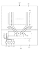
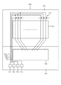
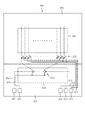
図6は、本発明の実施形態の変形例を示す概略図である。当該変形例では、上記実施の形態と異なり、パッド接続コンタクト610及び検査配線接続コンタクト620は、パッド330の配列方向、つまり、図6の左右の方向に、それぞれ千鳥配置されている。また、検査用トランジスタ710は、1つの検査用トランジスタ710毎に、パッド330の配列方向に千鳥配置されている。更に、ゲートメタル配線690、691は、上記実施の形態と異なり、2本配置されている。なお、ゲートメタル配線690、691は、その一端で接続されていてもよい。
Claims (12)
- 基板と、
基板上に設置されたドライバと、
前記ドライバの出力端子に接続される複数のパッドと、
前記複数のパッドとそれぞれ接続された複数の第1のコンタクトと、
前記複数の第1のコンタクトに対して設置された複数の第2のコンタクトと、
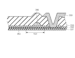
前記複数の第1及び第2のコンタクト間をそれぞれ延伸し接続する複数のポリシリコン膜と、
少なくとも1本のゲート配線を形成する、前記ポリシリコン膜とは異なる層に形成された金属層とを有し、
前記金属層は、隣接する少なくとも1以上のトランジスタ毎に千鳥配置された複数のトランジスタを、前記複数のポリシリコン膜を横切ることにより形成し、
前記複数のトランジスタを形成する部分の前記複数のポリシリコン膜の幅は、前記コンタクトと前記トランジスタとを接続する部分の幅よりも広いこと
を特徴とする表示パネル。 - 前記複数のトランジスタは、隣接する2以上のトランジスタからなる複数のトランジスタ列を含み、前記複数のトランジスタ列は、千鳥配置されていることを特徴とする請求項1に記載の表示パネル。
- 前記複数のトランジスタ列は、それぞれ4以下のトランジスタを有する特徴とする請求項2に記載の表示パネル。
- 前記複数のトランジスタ列は、前記複数の第1のコンタクト側から前記複数の第2のコンタクト側をみて、互いに重なっている部分を有することを特徴とする請求項2に記載の表示パネル。
- 前記複数のトランジスタ列の間に配置された各ポリシリコン膜の幅は、前記複数のトランジスタを構成する部分の前記複数のポリシリコン膜の幅よりも狭いことを特徴とする請求項2に記載の表示パネル。
- 前記金属層は、2本のゲート配線を有し、前記複数のトランジスタは、1のトランジスタ毎に千鳥配置されていることを特徴とする請求項1に記載の表示パネル。
- 前記複数の第1及び第2のコンタクトは、前記複数のパッドの配列方向に、千鳥配置されていることを特徴とする請求項6に記載の表示パネル。
- 前記複数の第1及び第2のコンタクトは、前記2本のゲート配線の間において、一列に並ぶコンタクト列を形成することを特徴とする請求項7に記載の表示パネル。
- 前記表示パネルは、更に、前記ポリシリコン膜及びゲート配線とは異なる層に形成された金属配線層に複数の金属配線を有し、前記複数の金属配線は、前記複数の第1及び第2のコンタクトとそれぞれ接続され、前記金属配線の幅は、前記複数の第1及び第2のコンタクトの幅よりも狭いことを特徴とする請求項7に記載の表示パネル。
- 前記ゲート配線は、前記コンタクト列を形成する前記複数の第1及び第2のコンタクトに接続された複数の金属配線を、横切ることを特徴とする請求項8に記載の表示パネル。
- 前記複数のトランジスタを形成する部分の前記複数のポリシリコン膜の幅は、前記複数の第1及び第2のコンタクトの幅よりも広いことを特徴とする請求項1に記載の表示パネル。
- 前記ポリシリコン膜と前記金属層の間に絶縁層を有することを特徴とする請求項1に記載の表示パネル。
Priority Applications (4)
| Application Number | Priority Date | Filing Date | Title |
|---|---|---|---|
| JP2009231968A JP5404289B2 (ja) | 2009-10-05 | 2009-10-05 | 表示パネル |
| US12/896,940 US8188481B2 (en) | 2009-10-05 | 2010-10-04 | Display panel |
| US13/476,346 US8546812B2 (en) | 2009-10-05 | 2012-05-21 | Display panel |
| US14/033,694 US9136279B2 (en) | 2009-10-05 | 2013-09-23 | Display panel |
Applications Claiming Priority (1)
| Application Number | Priority Date | Filing Date | Title |
|---|---|---|---|
| JP2009231968A JP5404289B2 (ja) | 2009-10-05 | 2009-10-05 | 表示パネル |
Publications (3)
| Publication Number | Publication Date |
|---|---|
| JP2011081092A JP2011081092A (ja) | 2011-04-21 |
| JP2011081092A5 JP2011081092A5 (ja) | 2012-11-22 |
| JP5404289B2 true JP5404289B2 (ja) | 2014-01-29 |
Family
ID=43822509
Family Applications (1)
| Application Number | Title | Priority Date | Filing Date |
|---|---|---|---|
| JP2009231968A Active JP5404289B2 (ja) | 2009-10-05 | 2009-10-05 | 表示パネル |
Country Status (2)
| Country | Link |
|---|---|
| US (3) | US8188481B2 (ja) |
| JP (1) | JP5404289B2 (ja) |
Families Citing this family (11)
| Publication number | Priority date | Publication date | Assignee | Title |
|---|---|---|---|---|
| JP5404289B2 (ja) * | 2009-10-05 | 2014-01-29 | 株式会社ジャパンディスプレイ | 表示パネル |
| WO2012161072A1 (ja) * | 2011-05-24 | 2012-11-29 | シャープ株式会社 | アクティブマトリクス基板、及び表示装置 |
| KR20140064553A (ko) * | 2012-11-20 | 2014-05-28 | 삼성디스플레이 주식회사 | 유기 발광 표시 장치 및 그 제조 방법 |
| JP6138480B2 (ja) * | 2012-12-20 | 2017-05-31 | 株式会社ジャパンディスプレイ | 表示装置 |
| JP2014134647A (ja) * | 2013-01-10 | 2014-07-24 | Mitsubishi Electric Corp | 表示装置及びその検査方法 |
| JP6168927B2 (ja) * | 2013-09-05 | 2017-07-26 | 株式会社ジャパンディスプレイ | 表示装置 |
| KR102312291B1 (ko) * | 2015-02-24 | 2021-10-15 | 삼성디스플레이 주식회사 | 표시장치 및 그의 검사방법 |
| CN108335658B (zh) * | 2018-03-15 | 2021-08-06 | 京东方科技集团股份有限公司 | 显示面板和显示测试装置 |
| CN108520882B (zh) * | 2018-04-11 | 2021-03-23 | Tcl华星光电技术有限公司 | 一种阵列基板及制造该阵列基板的掩膜板 |
| US11417257B2 (en) * | 2019-12-26 | 2022-08-16 | Lg Display Co., Ltd. | Display device |
| CN114255683B (zh) * | 2021-12-21 | 2024-03-22 | 武汉华星光电技术有限公司 | 显示面板 |
Family Cites Families (18)
| Publication number | Priority date | Publication date | Assignee | Title |
|---|---|---|---|---|
| US5745404A (en) * | 1995-12-05 | 1998-04-28 | Integrated Device Technology, In.C | ISRAM layout and structure |
| JP4106193B2 (ja) | 2000-03-06 | 2008-06-25 | 株式会社 日立ディスプレイズ | 液晶表示装置及びその製造方法 |
| TW527513B (en) * | 2000-03-06 | 2003-04-11 | Hitachi Ltd | Liquid crystal display device and manufacturing method thereof |
| KR100771516B1 (ko) * | 2001-01-20 | 2007-10-30 | 삼성전자주식회사 | 박막트랜지스터 액정표시장치 |
| US20030085855A1 (en) * | 2001-07-17 | 2003-05-08 | Kabushiki Kaisha Toshiba | Array substrate, method of inspecting array substrate, and liquid crystal display |
| JP3909572B2 (ja) * | 2001-09-28 | 2007-04-25 | 株式会社日立製作所 | 表示装置 |
| JP4006304B2 (ja) * | 2002-09-10 | 2007-11-14 | 株式会社 日立ディスプレイズ | 画像表示装置 |
| US7710739B2 (en) * | 2005-04-28 | 2010-05-04 | Semiconductor Energy Laboratory Co., Ltd. | Semiconductor device and display device |
| JP4869807B2 (ja) * | 2006-06-30 | 2012-02-08 | 株式会社 日立ディスプレイズ | 表示装置 |
| JP4834477B2 (ja) * | 2006-07-07 | 2011-12-14 | 東芝モバイルディスプレイ株式会社 | 表示装置 |
| JP2008145730A (ja) * | 2006-12-11 | 2008-06-26 | Seiko Epson Corp | 電気光学装置用基板及び電気光学装置、並びに電子機器 |
| JP2009020199A (ja) * | 2007-07-10 | 2009-01-29 | Mitsubishi Electric Corp | 表示パネル及びその製造方法 |
| JP2009092695A (ja) * | 2007-10-03 | 2009-04-30 | Toshiba Matsushita Display Technology Co Ltd | 液晶表示装置 |
| JP4448535B2 (ja) * | 2007-12-18 | 2010-04-14 | 株式会社 日立ディスプレイズ | 表示装置 |
| JP2009198590A (ja) * | 2008-02-19 | 2009-09-03 | Sharp Corp | 薄膜トランジスタアレイ基板及びその検査方法 |
| JP5024110B2 (ja) * | 2008-02-22 | 2012-09-12 | セイコーエプソン株式会社 | 電気光学装置及び電子機器 |
| JP5404289B2 (ja) * | 2009-10-05 | 2014-01-29 | 株式会社ジャパンディスプレイ | 表示パネル |
| JP5638833B2 (ja) * | 2010-04-22 | 2014-12-10 | 株式会社ジャパンディスプレイ | 画像表示装置及びその製造方法 |
-
2009
- 2009-10-05 JP JP2009231968A patent/JP5404289B2/ja active Active
-
2010
- 2010-10-04 US US12/896,940 patent/US8188481B2/en active Active
-
2012
- 2012-05-21 US US13/476,346 patent/US8546812B2/en active Active
-
2013
- 2013-09-23 US US14/033,694 patent/US9136279B2/en active Active
Also Published As
| Publication number | Publication date |
|---|---|
| US20120228610A1 (en) | 2012-09-13 |
| US20140021478A1 (en) | 2014-01-23 |
| JP2011081092A (ja) | 2011-04-21 |
| US8188481B2 (en) | 2012-05-29 |
| US8546812B2 (en) | 2013-10-01 |
| US20110079789A1 (en) | 2011-04-07 |
| US9136279B2 (en) | 2015-09-15 |
Similar Documents
| Publication | Publication Date | Title |
|---|---|---|
| JP5404289B2 (ja) | 表示パネル | |
| TWI388912B (zh) | 製造陣列基板之方法 | |
| TWI398712B (zh) | 具通至測試線之改良式連接結構的薄膜電晶體陣列面板 | |
| JP6681926B2 (ja) | アクティブマトリクス基板及び表示パネル | |
| KR20090126052A (ko) | 박막 트랜지스터 기판 및 이를 표함하는 표시 장치 | |
| JP2016057344A (ja) | 表示装置 | |
| JP2008003134A (ja) | 配線構造、及び表示装置 | |
| WO2017219702A1 (zh) | 一种显示基板、其制作方法及显示装置 | |
| WO2009081633A1 (ja) | アクティブマトリクス基板、これを備えた液晶表示装置、及びアクティブマトリクス基板の製造方法 | |
| JP2007192968A (ja) | 液晶表示装置 | |
| JP2007140378A (ja) | 表示装置 | |
| JP2008064961A (ja) | 配線構造、及び表示装置 | |
| JP2007219046A (ja) | 液晶表示パネル | |
| JP4995227B2 (ja) | 薄膜トランジスターにおけるマザーボードのテストラインおよびその製造方法 | |
| US7990486B2 (en) | Liquid crystal display panel with line defect repairing mechanism and repairing method thereof | |
| JP4725358B2 (ja) | カラー液晶表示パネル | |
| KR20030057043A (ko) | 박막 트랜지스터 검사용 단락 배선을 갖는 액정 표시장치 | |
| JP2011090288A (ja) | 薄膜トランジスタアレイパネル及びその製造方法 | |
| JP2009251417A (ja) | 液晶表示装置 | |
| JP2008089646A (ja) | 表示装置 | |
| JP2014149482A (ja) | 液晶表示装置 | |
| JP2010156867A (ja) | 薄膜トランジスタ基板前駆体及び薄膜トランジスタ基板の製造方法 | |
| US20120007082A1 (en) | Thin film transistor array panel | |
| KR100707009B1 (ko) | 박막 트랜지스터 액정표시소자 | |
| JP2007219047A (ja) | 液晶表示パネル |
Legal Events
| Date | Code | Title | Description |
|---|---|---|---|
| A521 | Request for written amendment filed |
Free format text: JAPANESE INTERMEDIATE CODE: A523 Effective date: 20121003 |
|
| A621 | Written request for application examination |
Free format text: JAPANESE INTERMEDIATE CODE: A621 Effective date: 20121003 |
|
| A977 | Report on retrieval |
Free format text: JAPANESE INTERMEDIATE CODE: A971007 Effective date: 20130523 |
|
| A131 | Notification of reasons for refusal |
Free format text: JAPANESE INTERMEDIATE CODE: A131 Effective date: 20130618 |
|
| A521 | Request for written amendment filed |
Free format text: JAPANESE INTERMEDIATE CODE: A523 Effective date: 20130812 |
|
| A977 | Report on retrieval |
Free format text: JAPANESE INTERMEDIATE CODE: A971007 Effective date: 20130812 |
|
| TRDD | Decision of grant or rejection written | ||
| A01 | Written decision to grant a patent or to grant a registration (utility model) |
Free format text: JAPANESE INTERMEDIATE CODE: A01 Effective date: 20131001 |
|
| A61 | First payment of annual fees (during grant procedure) |
Free format text: JAPANESE INTERMEDIATE CODE: A61 Effective date: 20131029 |
|
| R150 | Certificate of patent or registration of utility model |
Ref document number: 5404289 Country of ref document: JP Free format text: JAPANESE INTERMEDIATE CODE: R150 |
|
| R250 | Receipt of annual fees |
Free format text: JAPANESE INTERMEDIATE CODE: R250 |
|
| R250 | Receipt of annual fees |
Free format text: JAPANESE INTERMEDIATE CODE: R250 |
|
| R250 | Receipt of annual fees |
Free format text: JAPANESE INTERMEDIATE CODE: R250 |
|
| R250 | Receipt of annual fees |
Free format text: JAPANESE INTERMEDIATE CODE: R250 |
|
| R250 | Receipt of annual fees |
Free format text: JAPANESE INTERMEDIATE CODE: R250 |
|
| R250 | Receipt of annual fees |
Free format text: JAPANESE INTERMEDIATE CODE: R250 |
|
| R250 | Receipt of annual fees |
Free format text: JAPANESE INTERMEDIATE CODE: R250 |
|
| S111 | Request for change of ownership or part of ownership |
Free format text: JAPANESE INTERMEDIATE CODE: R313117 |
|
| R350 | Written notification of registration of transfer |
Free format text: JAPANESE INTERMEDIATE CODE: R350 |
|
| R250 | Receipt of annual fees |
Free format text: JAPANESE INTERMEDIATE CODE: R250 |