JP5341556B2 - 半導体装置の製造方法 - Google Patents
半導体装置の製造方法 Download PDFInfo
- Publication number
- JP5341556B2 JP5341556B2 JP2009046356A JP2009046356A JP5341556B2 JP 5341556 B2 JP5341556 B2 JP 5341556B2 JP 2009046356 A JP2009046356 A JP 2009046356A JP 2009046356 A JP2009046356 A JP 2009046356A JP 5341556 B2 JP5341556 B2 JP 5341556B2
- Authority
- JP
- Japan
- Prior art keywords
- island
- cavity
- lead
- runner
- resin
- Prior art date
- Legal status (The legal status is an assumption and is not a legal conclusion. Google has not performed a legal analysis and makes no representation as to the accuracy of the status listed.)
- Active
Links
- 239000004065 semiconductor Substances 0.000 title claims description 69
- 238000004519 manufacturing process Methods 0.000 title claims description 20
- 239000011347 resin Substances 0.000 claims description 111
- 229920005989 resin Polymers 0.000 claims description 111
- 238000007789 sealing Methods 0.000 claims description 61
- 238000000034 method Methods 0.000 claims description 19
- 239000002184 metal Substances 0.000 claims description 16
- 229910052751 metal Inorganic materials 0.000 claims description 16
- 238000002347 injection Methods 0.000 claims description 15
- 239000007924 injection Substances 0.000 claims description 15
- 229910001111 Fine metal Inorganic materials 0.000 claims description 7
- 238000003825 pressing Methods 0.000 description 6
- 239000007788 liquid Substances 0.000 description 4
- 229910052802 copper Inorganic materials 0.000 description 3
- 239000010949 copper Substances 0.000 description 3
- 239000000463 material Substances 0.000 description 3
- RYGMFSIKBFXOCR-UHFFFAOYSA-N Copper Chemical compound [Cu] RYGMFSIKBFXOCR-UHFFFAOYSA-N 0.000 description 2
- 238000013459 approach Methods 0.000 description 2
- 238000005520 cutting process Methods 0.000 description 2
- 239000011159 matrix material Substances 0.000 description 2
- 238000004080 punching Methods 0.000 description 2
- 239000000725 suspension Substances 0.000 description 2
- 230000015556 catabolic process Effects 0.000 description 1
- 230000006866 deterioration Effects 0.000 description 1
- 238000010586 diagram Methods 0.000 description 1
- 238000005538 encapsulation Methods 0.000 description 1
- 238000005530 etching Methods 0.000 description 1
- 230000005496 eutectics Effects 0.000 description 1
- 230000005669 field effect Effects 0.000 description 1
- PCHJSUWPFVWCPO-UHFFFAOYSA-N gold Chemical compound [Au] PCHJSUWPFVWCPO-UHFFFAOYSA-N 0.000 description 1
- 239000010931 gold Substances 0.000 description 1
- 229910052737 gold Inorganic materials 0.000 description 1
- 238000013007 heat curing Methods 0.000 description 1
- 238000010438 heat treatment Methods 0.000 description 1
- 238000001746 injection moulding Methods 0.000 description 1
- 230000001678 irradiating effect Effects 0.000 description 1
- 229910044991 metal oxide Inorganic materials 0.000 description 1
- 150000004706 metal oxides Chemical class 0.000 description 1
- 239000000203 mixture Substances 0.000 description 1
- 238000004806 packaging method and process Methods 0.000 description 1
- 238000000926 separation method Methods 0.000 description 1
- 229910000679 solder Inorganic materials 0.000 description 1
- 239000007787 solid Substances 0.000 description 1
- 230000009466 transformation Effects 0.000 description 1
- 238000011144 upstream manufacturing Methods 0.000 description 1
Images


Classifications
-
- H—ELECTRICITY
- H01—ELECTRIC ELEMENTS
- H01L—SEMICONDUCTOR DEVICES NOT COVERED BY CLASS H10
- H01L21/00—Processes or apparatus adapted for the manufacture or treatment of semiconductor or solid state devices or of parts thereof
- H01L21/02—Manufacture or treatment of semiconductor devices or of parts thereof
- H01L21/04—Manufacture or treatment of semiconductor devices or of parts thereof the devices having at least one potential-jump barrier or surface barrier, e.g. PN junction, depletion layer or carrier concentration layer
- H01L21/50—Assembly of semiconductor devices using processes or apparatus not provided for in a single one of the subgroups H01L21/06 - H01L21/326, e.g. sealing of a cap to a base of a container
- H01L21/56—Encapsulations, e.g. encapsulation layers, coatings
- H01L21/565—Moulds
-
- H—ELECTRICITY
- H01—ELECTRIC ELEMENTS
- H01L—SEMICONDUCTOR DEVICES NOT COVERED BY CLASS H10
- H01L23/00—Details of semiconductor or other solid state devices
- H01L23/48—Arrangements for conducting electric current to or from the solid state body in operation, e.g. leads, terminal arrangements ; Selection of materials therefor
- H01L23/488—Arrangements for conducting electric current to or from the solid state body in operation, e.g. leads, terminal arrangements ; Selection of materials therefor consisting of soldered or bonded constructions
- H01L23/495—Lead-frames or other flat leads
- H01L23/49541—Geometry of the lead-frame
- H01L23/49562—Geometry of the lead-frame for devices being provided for in H01L29/00
-
- H—ELECTRICITY
- H01—ELECTRIC ELEMENTS
- H01L—SEMICONDUCTOR DEVICES NOT COVERED BY CLASS H10
- H01L24/00—Arrangements for connecting or disconnecting semiconductor or solid-state bodies; Methods or apparatus related thereto
- H01L24/93—Batch processes
- H01L24/95—Batch processes at chip-level, i.e. with connecting carried out on a plurality of singulated devices, i.e. on diced chips
- H01L24/97—Batch processes at chip-level, i.e. with connecting carried out on a plurality of singulated devices, i.e. on diced chips the devices being connected to a common substrate, e.g. interposer, said common substrate being separable into individual assemblies after connecting
-
- H—ELECTRICITY
- H01—ELECTRIC ELEMENTS
- H01L—SEMICONDUCTOR DEVICES NOT COVERED BY CLASS H10
- H01L2224/00—Indexing scheme for arrangements for connecting or disconnecting semiconductor or solid-state bodies and methods related thereto as covered by H01L24/00
- H01L2224/01—Means for bonding being attached to, or being formed on, the surface to be connected, e.g. chip-to-package, die-attach, "first-level" interconnects; Manufacturing methods related thereto
- H01L2224/02—Bonding areas; Manufacturing methods related thereto
- H01L2224/04—Structure, shape, material or disposition of the bonding areas prior to the connecting process
- H01L2224/05—Structure, shape, material or disposition of the bonding areas prior to the connecting process of an individual bonding area
- H01L2224/0554—External layer
- H01L2224/0555—Shape
- H01L2224/05552—Shape in top view
- H01L2224/05554—Shape in top view being square
-
- H—ELECTRICITY
- H01—ELECTRIC ELEMENTS
- H01L—SEMICONDUCTOR DEVICES NOT COVERED BY CLASS H10
- H01L2224/00—Indexing scheme for arrangements for connecting or disconnecting semiconductor or solid-state bodies and methods related thereto as covered by H01L24/00
- H01L2224/01—Means for bonding being attached to, or being formed on, the surface to be connected, e.g. chip-to-package, die-attach, "first-level" interconnects; Manufacturing methods related thereto
- H01L2224/42—Wire connectors; Manufacturing methods related thereto
- H01L2224/44—Structure, shape, material or disposition of the wire connectors prior to the connecting process
- H01L2224/45—Structure, shape, material or disposition of the wire connectors prior to the connecting process of an individual wire connector
- H01L2224/45001—Core members of the connector
- H01L2224/45099—Material
- H01L2224/451—Material with a principal constituent of the material being a metal or a metalloid, e.g. boron (B), silicon (Si), germanium (Ge), arsenic (As), antimony (Sb), tellurium (Te) and polonium (Po), and alloys thereof
- H01L2224/45117—Material with a principal constituent of the material being a metal or a metalloid, e.g. boron (B), silicon (Si), germanium (Ge), arsenic (As), antimony (Sb), tellurium (Te) and polonium (Po), and alloys thereof the principal constituent melting at a temperature of greater than or equal to 400°C and less than 950°C
- H01L2224/45124—Aluminium (Al) as principal constituent
-
- H—ELECTRICITY
- H01—ELECTRIC ELEMENTS
- H01L—SEMICONDUCTOR DEVICES NOT COVERED BY CLASS H10
- H01L2224/00—Indexing scheme for arrangements for connecting or disconnecting semiconductor or solid-state bodies and methods related thereto as covered by H01L24/00
- H01L2224/01—Means for bonding being attached to, or being formed on, the surface to be connected, e.g. chip-to-package, die-attach, "first-level" interconnects; Manufacturing methods related thereto
- H01L2224/42—Wire connectors; Manufacturing methods related thereto
- H01L2224/44—Structure, shape, material or disposition of the wire connectors prior to the connecting process
- H01L2224/45—Structure, shape, material or disposition of the wire connectors prior to the connecting process of an individual wire connector
- H01L2224/45001—Core members of the connector
- H01L2224/45099—Material
- H01L2224/451—Material with a principal constituent of the material being a metal or a metalloid, e.g. boron (B), silicon (Si), germanium (Ge), arsenic (As), antimony (Sb), tellurium (Te) and polonium (Po), and alloys thereof
- H01L2224/45138—Material with a principal constituent of the material being a metal or a metalloid, e.g. boron (B), silicon (Si), germanium (Ge), arsenic (As), antimony (Sb), tellurium (Te) and polonium (Po), and alloys thereof the principal constituent melting at a temperature of greater than or equal to 950°C and less than 1550°C
- H01L2224/45144—Gold (Au) as principal constituent
-
- H—ELECTRICITY
- H01—ELECTRIC ELEMENTS
- H01L—SEMICONDUCTOR DEVICES NOT COVERED BY CLASS H10
- H01L2224/00—Indexing scheme for arrangements for connecting or disconnecting semiconductor or solid-state bodies and methods related thereto as covered by H01L24/00
- H01L2224/01—Means for bonding being attached to, or being formed on, the surface to be connected, e.g. chip-to-package, die-attach, "first-level" interconnects; Manufacturing methods related thereto
- H01L2224/42—Wire connectors; Manufacturing methods related thereto
- H01L2224/44—Structure, shape, material or disposition of the wire connectors prior to the connecting process
- H01L2224/45—Structure, shape, material or disposition of the wire connectors prior to the connecting process of an individual wire connector
- H01L2224/45001—Core members of the connector
- H01L2224/45099—Material
- H01L2224/451—Material with a principal constituent of the material being a metal or a metalloid, e.g. boron (B), silicon (Si), germanium (Ge), arsenic (As), antimony (Sb), tellurium (Te) and polonium (Po), and alloys thereof
- H01L2224/45138—Material with a principal constituent of the material being a metal or a metalloid, e.g. boron (B), silicon (Si), germanium (Ge), arsenic (As), antimony (Sb), tellurium (Te) and polonium (Po), and alloys thereof the principal constituent melting at a temperature of greater than or equal to 950°C and less than 1550°C
- H01L2224/45147—Copper (Cu) as principal constituent
-
- H—ELECTRICITY
- H01—ELECTRIC ELEMENTS
- H01L—SEMICONDUCTOR DEVICES NOT COVERED BY CLASS H10
- H01L2224/00—Indexing scheme for arrangements for connecting or disconnecting semiconductor or solid-state bodies and methods related thereto as covered by H01L24/00
- H01L2224/01—Means for bonding being attached to, or being formed on, the surface to be connected, e.g. chip-to-package, die-attach, "first-level" interconnects; Manufacturing methods related thereto
- H01L2224/42—Wire connectors; Manufacturing methods related thereto
- H01L2224/47—Structure, shape, material or disposition of the wire connectors after the connecting process
- H01L2224/48—Structure, shape, material or disposition of the wire connectors after the connecting process of an individual wire connector
- H01L2224/4805—Shape
- H01L2224/4809—Loop shape
- H01L2224/48091—Arched
-
- H—ELECTRICITY
- H01—ELECTRIC ELEMENTS
- H01L—SEMICONDUCTOR DEVICES NOT COVERED BY CLASS H10
- H01L2224/00—Indexing scheme for arrangements for connecting or disconnecting semiconductor or solid-state bodies and methods related thereto as covered by H01L24/00
- H01L2224/01—Means for bonding being attached to, or being formed on, the surface to be connected, e.g. chip-to-package, die-attach, "first-level" interconnects; Manufacturing methods related thereto
- H01L2224/42—Wire connectors; Manufacturing methods related thereto
- H01L2224/47—Structure, shape, material or disposition of the wire connectors after the connecting process
- H01L2224/48—Structure, shape, material or disposition of the wire connectors after the connecting process of an individual wire connector
- H01L2224/481—Disposition
- H01L2224/48151—Connecting between a semiconductor or solid-state body and an item not being a semiconductor or solid-state body, e.g. chip-to-substrate, chip-to-passive
- H01L2224/48221—Connecting between a semiconductor or solid-state body and an item not being a semiconductor or solid-state body, e.g. chip-to-substrate, chip-to-passive the body and the item being stacked
- H01L2224/48245—Connecting between a semiconductor or solid-state body and an item not being a semiconductor or solid-state body, e.g. chip-to-substrate, chip-to-passive the body and the item being stacked the item being metallic
- H01L2224/48247—Connecting between a semiconductor or solid-state body and an item not being a semiconductor or solid-state body, e.g. chip-to-substrate, chip-to-passive the body and the item being stacked the item being metallic connecting the wire to a bond pad of the item
-
- H—ELECTRICITY
- H01—ELECTRIC ELEMENTS
- H01L—SEMICONDUCTOR DEVICES NOT COVERED BY CLASS H10
- H01L2224/00—Indexing scheme for arrangements for connecting or disconnecting semiconductor or solid-state bodies and methods related thereto as covered by H01L24/00
- H01L2224/01—Means for bonding being attached to, or being formed on, the surface to be connected, e.g. chip-to-package, die-attach, "first-level" interconnects; Manufacturing methods related thereto
- H01L2224/42—Wire connectors; Manufacturing methods related thereto
- H01L2224/47—Structure, shape, material or disposition of the wire connectors after the connecting process
- H01L2224/48—Structure, shape, material or disposition of the wire connectors after the connecting process of an individual wire connector
- H01L2224/484—Connecting portions
- H01L2224/4847—Connecting portions the connecting portion on the bonding area of the semiconductor or solid-state body being a wedge bond
- H01L2224/48472—Connecting portions the connecting portion on the bonding area of the semiconductor or solid-state body being a wedge bond the other connecting portion not on the bonding area also being a wedge bond, i.e. wedge-to-wedge
-
- H—ELECTRICITY
- H01—ELECTRIC ELEMENTS
- H01L—SEMICONDUCTOR DEVICES NOT COVERED BY CLASS H10
- H01L2224/00—Indexing scheme for arrangements for connecting or disconnecting semiconductor or solid-state bodies and methods related thereto as covered by H01L24/00
- H01L2224/01—Means for bonding being attached to, or being formed on, the surface to be connected, e.g. chip-to-package, die-attach, "first-level" interconnects; Manufacturing methods related thereto
- H01L2224/42—Wire connectors; Manufacturing methods related thereto
- H01L2224/47—Structure, shape, material or disposition of the wire connectors after the connecting process
- H01L2224/49—Structure, shape, material or disposition of the wire connectors after the connecting process of a plurality of wire connectors
- H01L2224/491—Disposition
- H01L2224/4912—Layout
- H01L2224/49171—Fan-out arrangements
-
- H—ELECTRICITY
- H01—ELECTRIC ELEMENTS
- H01L—SEMICONDUCTOR DEVICES NOT COVERED BY CLASS H10
- H01L2224/00—Indexing scheme for arrangements for connecting or disconnecting semiconductor or solid-state bodies and methods related thereto as covered by H01L24/00
- H01L2224/93—Batch processes
- H01L2224/95—Batch processes at chip-level, i.e. with connecting carried out on a plurality of singulated devices, i.e. on diced chips
- H01L2224/97—Batch processes at chip-level, i.e. with connecting carried out on a plurality of singulated devices, i.e. on diced chips the devices being connected to a common substrate, e.g. interposer, said common substrate being separable into individual assemblies after connecting
-
- H—ELECTRICITY
- H01—ELECTRIC ELEMENTS
- H01L—SEMICONDUCTOR DEVICES NOT COVERED BY CLASS H10
- H01L24/00—Arrangements for connecting or disconnecting semiconductor or solid-state bodies; Methods or apparatus related thereto
- H01L24/01—Means for bonding being attached to, or being formed on, the surface to be connected, e.g. chip-to-package, die-attach, "first-level" interconnects; Manufacturing methods related thereto
- H01L24/42—Wire connectors; Manufacturing methods related thereto
- H01L24/44—Structure, shape, material or disposition of the wire connectors prior to the connecting process
- H01L24/45—Structure, shape, material or disposition of the wire connectors prior to the connecting process of an individual wire connector
-
- H—ELECTRICITY
- H01—ELECTRIC ELEMENTS
- H01L—SEMICONDUCTOR DEVICES NOT COVERED BY CLASS H10
- H01L24/00—Arrangements for connecting or disconnecting semiconductor or solid-state bodies; Methods or apparatus related thereto
- H01L24/01—Means for bonding being attached to, or being formed on, the surface to be connected, e.g. chip-to-package, die-attach, "first-level" interconnects; Manufacturing methods related thereto
- H01L24/42—Wire connectors; Manufacturing methods related thereto
- H01L24/47—Structure, shape, material or disposition of the wire connectors after the connecting process
- H01L24/48—Structure, shape, material or disposition of the wire connectors after the connecting process of an individual wire connector
-
- H—ELECTRICITY
- H01—ELECTRIC ELEMENTS
- H01L—SEMICONDUCTOR DEVICES NOT COVERED BY CLASS H10
- H01L24/00—Arrangements for connecting or disconnecting semiconductor or solid-state bodies; Methods or apparatus related thereto
- H01L24/01—Means for bonding being attached to, or being formed on, the surface to be connected, e.g. chip-to-package, die-attach, "first-level" interconnects; Manufacturing methods related thereto
- H01L24/42—Wire connectors; Manufacturing methods related thereto
- H01L24/47—Structure, shape, material or disposition of the wire connectors after the connecting process
- H01L24/49—Structure, shape, material or disposition of the wire connectors after the connecting process of a plurality of wire connectors
-
- H—ELECTRICITY
- H01—ELECTRIC ELEMENTS
- H01L—SEMICONDUCTOR DEVICES NOT COVERED BY CLASS H10
- H01L2924/00—Indexing scheme for arrangements or methods for connecting or disconnecting semiconductor or solid-state bodies as covered by H01L24/00
- H01L2924/0001—Technical content checked by a classifier
- H01L2924/00014—Technical content checked by a classifier the subject-matter covered by the group, the symbol of which is combined with the symbol of this group, being disclosed without further technical details
-
- H—ELECTRICITY
- H01—ELECTRIC ELEMENTS
- H01L—SEMICONDUCTOR DEVICES NOT COVERED BY CLASS H10
- H01L2924/00—Indexing scheme for arrangements or methods for connecting or disconnecting semiconductor or solid-state bodies as covered by H01L24/00
- H01L2924/01—Chemical elements
- H01L2924/01005—Boron [B]
-
- H—ELECTRICITY
- H01—ELECTRIC ELEMENTS
- H01L—SEMICONDUCTOR DEVICES NOT COVERED BY CLASS H10
- H01L2924/00—Indexing scheme for arrangements or methods for connecting or disconnecting semiconductor or solid-state bodies as covered by H01L24/00
- H01L2924/01—Chemical elements
- H01L2924/01006—Carbon [C]
-
- H—ELECTRICITY
- H01—ELECTRIC ELEMENTS
- H01L—SEMICONDUCTOR DEVICES NOT COVERED BY CLASS H10
- H01L2924/00—Indexing scheme for arrangements or methods for connecting or disconnecting semiconductor or solid-state bodies as covered by H01L24/00
- H01L2924/01—Chemical elements
- H01L2924/01013—Aluminum [Al]
-
- H—ELECTRICITY
- H01—ELECTRIC ELEMENTS
- H01L—SEMICONDUCTOR DEVICES NOT COVERED BY CLASS H10
- H01L2924/00—Indexing scheme for arrangements or methods for connecting or disconnecting semiconductor or solid-state bodies as covered by H01L24/00
- H01L2924/01—Chemical elements
- H01L2924/01029—Copper [Cu]
-
- H—ELECTRICITY
- H01—ELECTRIC ELEMENTS
- H01L—SEMICONDUCTOR DEVICES NOT COVERED BY CLASS H10
- H01L2924/00—Indexing scheme for arrangements or methods for connecting or disconnecting semiconductor or solid-state bodies as covered by H01L24/00
- H01L2924/01—Chemical elements
- H01L2924/01033—Arsenic [As]
-
- H—ELECTRICITY
- H01—ELECTRIC ELEMENTS
- H01L—SEMICONDUCTOR DEVICES NOT COVERED BY CLASS H10
- H01L2924/00—Indexing scheme for arrangements or methods for connecting or disconnecting semiconductor or solid-state bodies as covered by H01L24/00
- H01L2924/01—Chemical elements
- H01L2924/01047—Silver [Ag]
-
- H—ELECTRICITY
- H01—ELECTRIC ELEMENTS
- H01L—SEMICONDUCTOR DEVICES NOT COVERED BY CLASS H10
- H01L2924/00—Indexing scheme for arrangements or methods for connecting or disconnecting semiconductor or solid-state bodies as covered by H01L24/00
- H01L2924/01—Chemical elements
- H01L2924/01079—Gold [Au]
-
- H—ELECTRICITY
- H01—ELECTRIC ELEMENTS
- H01L—SEMICONDUCTOR DEVICES NOT COVERED BY CLASS H10
- H01L2924/00—Indexing scheme for arrangements or methods for connecting or disconnecting semiconductor or solid-state bodies as covered by H01L24/00
- H01L2924/01—Chemical elements
- H01L2924/01082—Lead [Pb]
-
- H—ELECTRICITY
- H01—ELECTRIC ELEMENTS
- H01L—SEMICONDUCTOR DEVICES NOT COVERED BY CLASS H10
- H01L2924/00—Indexing scheme for arrangements or methods for connecting or disconnecting semiconductor or solid-state bodies as covered by H01L24/00
- H01L2924/013—Alloys
- H01L2924/0132—Binary Alloys
- H01L2924/01322—Eutectic Alloys, i.e. obtained by a liquid transforming into two solid phases
-
- H—ELECTRICITY
- H01—ELECTRIC ELEMENTS
- H01L—SEMICONDUCTOR DEVICES NOT COVERED BY CLASS H10
- H01L2924/00—Indexing scheme for arrangements or methods for connecting or disconnecting semiconductor or solid-state bodies as covered by H01L24/00
- H01L2924/10—Details of semiconductor or other solid state devices to be connected
- H01L2924/11—Device type
- H01L2924/12—Passive devices, e.g. 2 terminal devices
- H01L2924/1204—Optical Diode
- H01L2924/12041—LED
-
- H—ELECTRICITY
- H01—ELECTRIC ELEMENTS
- H01L—SEMICONDUCTOR DEVICES NOT COVERED BY CLASS H10
- H01L2924/00—Indexing scheme for arrangements or methods for connecting or disconnecting semiconductor or solid-state bodies as covered by H01L24/00
- H01L2924/10—Details of semiconductor or other solid state devices to be connected
- H01L2924/11—Device type
- H01L2924/13—Discrete devices, e.g. 3 terminal devices
- H01L2924/1304—Transistor
- H01L2924/1305—Bipolar Junction Transistor [BJT]
- H01L2924/13055—Insulated gate bipolar transistor [IGBT]
-
- H—ELECTRICITY
- H01—ELECTRIC ELEMENTS
- H01L—SEMICONDUCTOR DEVICES NOT COVERED BY CLASS H10
- H01L2924/00—Indexing scheme for arrangements or methods for connecting or disconnecting semiconductor or solid-state bodies as covered by H01L24/00
- H01L2924/10—Details of semiconductor or other solid state devices to be connected
- H01L2924/11—Device type
- H01L2924/13—Discrete devices, e.g. 3 terminal devices
- H01L2924/1304—Transistor
- H01L2924/1306—Field-effect transistor [FET]
- H01L2924/13091—Metal-Oxide-Semiconductor Field-Effect Transistor [MOSFET]
-
- H—ELECTRICITY
- H01—ELECTRIC ELEMENTS
- H01L—SEMICONDUCTOR DEVICES NOT COVERED BY CLASS H10
- H01L2924/00—Indexing scheme for arrangements or methods for connecting or disconnecting semiconductor or solid-state bodies as covered by H01L24/00
- H01L2924/10—Details of semiconductor or other solid state devices to be connected
- H01L2924/11—Device type
- H01L2924/14—Integrated circuits
-
- H—ELECTRICITY
- H01—ELECTRIC ELEMENTS
- H01L—SEMICONDUCTOR DEVICES NOT COVERED BY CLASS H10
- H01L2924/00—Indexing scheme for arrangements or methods for connecting or disconnecting semiconductor or solid-state bodies as covered by H01L24/00
- H01L2924/15—Details of package parts other than the semiconductor or other solid state devices to be connected
- H01L2924/181—Encapsulation
Description
特開平1−205432号公報
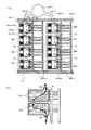
キャビティ36Aは、アイランド12が図示され、キャビティ36Bは、リードLが図示されている。本来この二つのキャビティには、同じものが封止されるが、ここでは図面の都合上、別のものを示した。
両方ともにアイランドを有し、そのアイランドの裏面が封止されるタイプである。よってアイランド12の裏面と下金型LDの間は、その隙間が狭く、未充填部分が無いようにするためにも、注入口P2は、アイランド12の高さとほぼ同等か、または±100μmの間に位置する。また隙間が裏面にあると言う事は、その厚さ分変動し易いと言う事になる。
図3(B)は図3(A)を部分的に拡大して示す平面図である。ここでは、上側の外枠52と下側の外枠52とを連続させるように、タイバー58が延在している。紙面上では、左側にユニット56A−56Dが一列に配置されてタイバー58により連結され、右側にユニット56E−56Hが一列に配置されてタイバー58により連結されている。各ユニットは、アイランド12と、リード14A、14B、14Cから成る。そして、リード14A、14Cの一端はアイランド12に接近すると共に、リード14Bはアイランド12と一体的に導出している。ユニット56Aのリード14A、14B、14Cの中間部および端部は、タイバー58と連続している。同様に、他のユニット56B−56Dもタイバー58と連続している。また、右側に一列に配置されるユニット56E−56Hのリードもタイバー58により連結されている。ここで、横方向に隣接するユニットのリードは、千鳥状に配置されても良い。この場合は、例えば、ユニット56Aのリード14A−14Cと、ユニット56Eのリード14A−14Cが対向して千鳥状に配置される。
しかしながら本発明では、このP1を従来よりも押し上げ、溶融樹脂がアイランド12に力を作用させる前で、隣のキャビティ36Bに射出させている。このことにより、封止樹脂16がアイランド12に与える圧力が低減されて、結果的にアイランド12の下方への移動が抑制される。
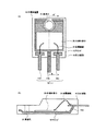
以上の工程を経て、図2に示す構成の半導体装置10が製造される。
12 アイランド
14,14A,14B,14C リード
16 封止樹脂
20 半導体素子
22 貫通孔
24 金属細線
30 金型
32 上金型
34 下金型
36,36A,36B,36C,36D,36E キャビティ
38 ランナー
40 プランジャー
42 ポッド
44 ランナー
50 リードフレーム
52 外枠
54 ブロック
56、56A、56B、56C、56D、56E、56F、56G、56H ユニット
58 タイバー
Claims (4)
- 第1の方向に沿って複数のキャビティを整列して配置し、隣接するキャビティの間をランナーを介して互いに連通した金型を用意する工程と、
前記金型にリードフレームを配置し、前記リードフレームに含まれるアイランド、前記アイランドの近傍に一端が配置されたリード、前記アイランドに固着された半導体素子および前記リードと前記半導体素子とを接続する金属細線を各々の前記キャビティに収納する工程と、
前記ランナーを介して前記複数のキャビティに封止樹脂を注入し、前記アイランド、前記リード、前記半導体素子および前記金属細線を前記封止樹脂で封止する工程と、を具備する半導体装置の製造方法に於いて、
前記封止する工程では、一のキャビティから前記一のキャビティの排出口を経由して前記ランナーに排出された前記封止樹脂を、前記ランナーから前記一のキャビティに隣接する他のキャビティの注入口を経由して前記他のキャビティに注入するとともに、
平面視において、前記キャビティの排出口と注入口とを前記一方向に対して右または左のどちらか偏った位置に交互に配置し、
断面視において、前記排出口を前記注入口よりも上方に配置したことを特徴とする半導体装置の製造方法。 - 前記キャビティには前記ランナーを介して連通した第1キャビティと第2キャビティが含まれ、
平面視で、前記第1キャビティの前記排出口は前記キャビティの右または左のどちらか一方に偏った位置に配置され、
平面視で、前記第2キャビティの前記排出口は前記キャビティの右または左のどちらか他方に偏った位置に配置され、
前記第1キャビティと前記第2キャビティを通過する前記封止樹脂は蛇行しながら注入されることを特徴とする請求項1に記載の半導体装置の製造方法。 - 前記封止樹脂が硬化した後、前記金型から前記半導体装置を取り出し、前記ランナーに充填された前記封止樹脂を取り除き、前記半導体装置の側面に切除痕を設けることを特徴とする請求項1または請求項2に記載の半導体装置の製造方法。
- 前記アイランドは、前記注入口に接近する第1側辺と、前記第1側辺に対向して前記排出口に接近する第2側辺と、前記第1側辺とは交差してなる第3側辺と、前記第3側辺に対向する第4側辺とを有し、
前記リードフレームには、前記アイランドの前記第1側辺および前記第2側辺と連続する保持リードが含まれ、
金属細線が接続される前記リードの一端は、前記アイランドの前記第3側辺および前記第4側辺の近傍に配置されることを特徴とする請求項1から請求項3の何れかに記載の半導体装置の製造方法。
Priority Applications (3)
| Application Number | Priority Date | Filing Date | Title |
|---|---|---|---|
| JP2009046356A JP5341556B2 (ja) | 2008-09-30 | 2009-02-27 | 半導体装置の製造方法 |
| US12/568,486 US8105883B2 (en) | 2008-09-30 | 2009-09-28 | Molding die with tilted runner, method of manufacturing semiconductor device using the same, and semiconductor device made by the method |
| CN200910179607XA CN101930933B (zh) | 2008-09-30 | 2009-09-29 | 半导体装置及其制造方法 |
Applications Claiming Priority (3)
| Application Number | Priority Date | Filing Date | Title |
|---|---|---|---|
| JP2008252996 | 2008-09-30 | ||
| JP2008252996 | 2008-09-30 | ||
| JP2009046356A JP5341556B2 (ja) | 2008-09-30 | 2009-02-27 | 半導体装置の製造方法 |
Publications (3)
| Publication Number | Publication Date |
|---|---|
| JP2010109315A JP2010109315A (ja) | 2010-05-13 |
| JP2010109315A5 JP2010109315A5 (ja) | 2012-03-15 |
| JP5341556B2 true JP5341556B2 (ja) | 2013-11-13 |
Family
ID=42298426
Family Applications (2)
| Application Number | Title | Priority Date | Filing Date |
|---|---|---|---|
| JP2009046356A Active JP5341556B2 (ja) | 2008-09-30 | 2009-02-27 | 半導体装置の製造方法 |
| JP2009046355A Active JP5147758B2 (ja) | 2008-09-30 | 2009-02-27 | 半導体装置の製造方法、半導体装置およびモールド金型 |
Family Applications After (1)
| Application Number | Title | Priority Date | Filing Date |
|---|---|---|---|
| JP2009046355A Active JP5147758B2 (ja) | 2008-09-30 | 2009-02-27 | 半導体装置の製造方法、半導体装置およびモールド金型 |
Country Status (3)
| Country | Link |
|---|---|
| US (1) | US8105883B2 (ja) |
| JP (2) | JP5341556B2 (ja) |
| CN (1) | CN101930933B (ja) |
Families Citing this family (13)
| Publication number | Priority date | Publication date | Assignee | Title |
|---|---|---|---|---|
| JP5761585B2 (ja) * | 2008-10-07 | 2015-08-12 | 国立研究開発法人情報通信研究機構 | パルスレーダ装置 |
| JP4852088B2 (ja) * | 2008-11-04 | 2012-01-11 | 株式会社東芝 | バイアス回路 |
| JP5333402B2 (ja) * | 2010-10-06 | 2013-11-06 | 三菱電機株式会社 | 半導体装置の製造方法 |
| CN102856217B (zh) * | 2011-06-30 | 2018-05-22 | 恩智浦美国有限公司 | 用于模塑半导体器件的装置和方法 |
| DE102012207678A1 (de) * | 2012-05-09 | 2013-11-14 | Osram Opto Semiconductors Gmbh | Vorrichtung zum formen einer gehäusestruktur für eine mehrzahl von elektronischen bauteilen und gehäusestruktur für eine mehrzahl von elektronischen bauteilen |
| US9911838B2 (en) * | 2012-10-26 | 2018-03-06 | Ixys Corporation | IGBT die structure with auxiliary P well terminal |
| US9947613B2 (en) | 2014-11-07 | 2018-04-17 | Mitsubishi Electric Corporation | Power semiconductor device and method for manufacturing the same |
| US9583421B2 (en) | 2015-07-16 | 2017-02-28 | Semiconductor Components Industries, Llc | Recessed lead leadframe packages |
| CN107645874A (zh) * | 2016-07-20 | 2018-01-30 | 珠海市声驰电器有限公司 | 一种密封电路结构及其灌封方法 |
| CN107731775A (zh) * | 2017-09-26 | 2018-02-23 | 铜陵中锐电子科技有限公司 | 适用于连续充填技术的to251型八排引线框架 |
| JP2020123691A (ja) * | 2019-01-31 | 2020-08-13 | 株式会社三社電機製作所 | 半導体製品 |
| US20210043466A1 (en) * | 2019-08-06 | 2021-02-11 | Texas Instruments Incorporated | Universal semiconductor package molds |
| JPWO2022259395A1 (ja) * | 2021-06-09 | 2022-12-15 |
Family Cites Families (10)
| Publication number | Priority date | Publication date | Assignee | Title |
|---|---|---|---|---|
| JPS6315432A (ja) * | 1986-07-08 | 1988-01-22 | Fujitsu Ltd | 樹脂パツケ−ジ成形用金型 |
| US4946633A (en) * | 1987-04-27 | 1990-08-07 | Hitachi, Ltd. | Method of producing semiconductor devices |
| JP2786197B2 (ja) | 1987-04-27 | 1998-08-13 | 株式会社日立製作所 | 半導体装置の製造方法 |
| JP2724491B2 (ja) * | 1989-02-01 | 1998-03-09 | 株式会社日立製作所 | 成形装置 |
| JPH04225241A (ja) * | 1990-12-26 | 1992-08-14 | Oki Electric Ind Co Ltd | 樹脂封止半導体装置の製造方法及びリードフレーム |
| JP3828036B2 (ja) * | 2002-03-28 | 2006-09-27 | 三菱電機株式会社 | 樹脂モールド型デバイスの製造方法及び製造装置 |
| JP4121335B2 (ja) * | 2002-08-28 | 2008-07-23 | 三洋電機株式会社 | リードフレームおよびそれを用いた半導体装置の製造方法 |
| JP2004158539A (ja) | 2002-11-05 | 2004-06-03 | Matsushita Electric Ind Co Ltd | 樹脂封止型半導体装置の製造方法 |
| JP4243177B2 (ja) * | 2003-12-22 | 2009-03-25 | 株式会社ルネサステクノロジ | 半導体装置の製造方法 |
| WO2006129926A1 (en) * | 2005-06-02 | 2006-12-07 | Tsp Co., Ltd. | Mold for manufacturing semiconductor device and semiconductor device manufactred using the same |
-
2009
- 2009-02-27 JP JP2009046356A patent/JP5341556B2/ja active Active
- 2009-02-27 JP JP2009046355A patent/JP5147758B2/ja active Active
- 2009-09-28 US US12/568,486 patent/US8105883B2/en active Active
- 2009-09-29 CN CN200910179607XA patent/CN101930933B/zh not_active Expired - Fee Related
Also Published As
| Publication number | Publication date |
|---|---|
| JP2010109314A (ja) | 2010-05-13 |
| US8105883B2 (en) | 2012-01-31 |
| US20100219517A1 (en) | 2010-09-02 |
| JP5147758B2 (ja) | 2013-02-20 |
| CN101930933A (zh) | 2010-12-29 |
| JP2010109315A (ja) | 2010-05-13 |
| CN101930933B (zh) | 2012-04-18 |
Similar Documents
| Publication | Publication Date | Title |
|---|---|---|
| JP5341556B2 (ja) | 半導体装置の製造方法 | |
| US20170133304A1 (en) | Low Profile Leaded Semiconductor Package | |
| US7781262B2 (en) | Method for producing semiconductor device and semiconductor device | |
| US7598603B2 (en) | Electronic component having a power switch with an anode thereof mounted on a die attach region of a heat sink | |
| US20120181676A1 (en) | Power semiconductor device packaging | |
| TWI650840B (zh) | 引線支架、半導體裝置及引線支架之製造方法 | |
| US20130017652A1 (en) | Method of manufacturing a semiconductor device package with a heatsink | |
| JP6539727B2 (ja) | 分配機能タイバーを有するギャングクリップ | |
| JP5180722B2 (ja) | 半導体装置の製造方法 | |
| US8633511B2 (en) | Method of producing semiconductor device packaging having chips attached to islands separately and covered by encapsulation material | |
| US6893898B2 (en) | Semiconductor device and a method of manufacturing the same | |
| JP3877409B2 (ja) | 半導体装置の製造方法 | |
| JP3877453B2 (ja) | 半導体装置の製造方法 | |
| JP3877410B2 (ja) | 半導体装置の製造方法 | |
| JP2004363365A (ja) | 半導体装置及びその製造方法 | |
| JP3877402B2 (ja) | 半導体装置の製造方法 | |
| JP4784945B2 (ja) | 半導体装置の製造方法 | |
| US20230038411A1 (en) | Semiconductor package with raised dam on clip or leadframe | |
| JP3831504B2 (ja) | リードフレーム | |
| US20050073031A1 (en) | Lead frame, semiconductor device, and method for manufacturing semiconductor device | |
| JP4887346B2 (ja) | 半導体装置 | |
| WO2006061673A1 (en) | Semiconductor package having at least two semiconductor chips and method of assembling the semiconductor package | |
| JP5086315B2 (ja) | 半導体装置の製造方法 | |
| JP5341473B2 (ja) | 半導体装置およびその製造方法 | |
| JP4383436B2 (ja) | 半導体装置 |
Legal Events
| Date | Code | Title | Description |
|---|---|---|---|
| A711 | Notification of change in applicant |
Free format text: JAPANESE INTERMEDIATE CODE: A711 Effective date: 20110613 |
|
| A621 | Written request for application examination |
Free format text: JAPANESE INTERMEDIATE CODE: A621 Effective date: 20120123 |
|
| A521 | Request for written amendment filed |
Free format text: JAPANESE INTERMEDIATE CODE: A523 Effective date: 20120131 |
|
| A977 | Report on retrieval |
Free format text: JAPANESE INTERMEDIATE CODE: A971007 Effective date: 20120905 |
|
| A131 | Notification of reasons for refusal |
Free format text: JAPANESE INTERMEDIATE CODE: A131 Effective date: 20120911 |
|
| A521 | Request for written amendment filed |
Free format text: JAPANESE INTERMEDIATE CODE: A523 Effective date: 20121207 |
|
| A711 | Notification of change in applicant |
Free format text: JAPANESE INTERMEDIATE CODE: A711 Effective date: 20130218 |
|
| A131 | Notification of reasons for refusal |
Free format text: JAPANESE INTERMEDIATE CODE: A131 Effective date: 20130226 |
|
| A521 | Request for written amendment filed |
Free format text: JAPANESE INTERMEDIATE CODE: A523 Effective date: 20130408 |
|
| A521 | Request for written amendment filed |
Free format text: JAPANESE INTERMEDIATE CODE: A523 Effective date: 20130524 |
|
| TRDD | Decision of grant or rejection written | ||
| A01 | Written decision to grant a patent or to grant a registration (utility model) |
Free format text: JAPANESE INTERMEDIATE CODE: A01 Effective date: 20130723 |
|
| A61 | First payment of annual fees (during grant procedure) |
Free format text: JAPANESE INTERMEDIATE CODE: A61 Effective date: 20130808 |
|
| R150 | Certificate of patent or registration of utility model |
Ref document number: 5341556 Country of ref document: JP Free format text: JAPANESE INTERMEDIATE CODE: R150 Free format text: JAPANESE INTERMEDIATE CODE: R150 |
|
| RD04 | Notification of resignation of power of attorney |
Free format text: JAPANESE INTERMEDIATE CODE: R3D04 |
|
| R250 | Receipt of annual fees |
Free format text: JAPANESE INTERMEDIATE CODE: R250 |
|
| R250 | Receipt of annual fees |
Free format text: JAPANESE INTERMEDIATE CODE: R250 |
|
| R250 | Receipt of annual fees |
Free format text: JAPANESE INTERMEDIATE CODE: R250 |
|
| R250 | Receipt of annual fees |
Free format text: JAPANESE INTERMEDIATE CODE: R250 |
|
| R250 | Receipt of annual fees |
Free format text: JAPANESE INTERMEDIATE CODE: R250 |
|
| R250 | Receipt of annual fees |
Free format text: JAPANESE INTERMEDIATE CODE: R250 |
|
| R250 | Receipt of annual fees |
Free format text: JAPANESE INTERMEDIATE CODE: R250 |
|
| R250 | Receipt of annual fees |
Free format text: JAPANESE INTERMEDIATE CODE: R250 |