JP5300184B2 - 圧電体、圧電体素子、圧電体素子を用いた液体吐出ヘッド及び液体吐出装置 - Google Patents
圧電体、圧電体素子、圧電体素子を用いた液体吐出ヘッド及び液体吐出装置 Download PDFInfo
- Publication number
- JP5300184B2 JP5300184B2 JP2006196114A JP2006196114A JP5300184B2 JP 5300184 B2 JP5300184 B2 JP 5300184B2 JP 2006196114 A JP2006196114 A JP 2006196114A JP 2006196114 A JP2006196114 A JP 2006196114A JP 5300184 B2 JP5300184 B2 JP 5300184B2
- Authority
- JP
- Japan
- Prior art keywords
- piezoelectric
- film
- substrate
- domain
- crystal
- Prior art date
- Legal status (The legal status is an assumption and is not a legal conclusion. Google has not performed a legal analysis and makes no representation as to the accuracy of the status listed.)
- Expired - Fee Related
Links
- 239000007788 liquid Substances 0.000 title claims description 161
- 239000013078 crystal Substances 0.000 claims abstract description 150
- RKTYLMNFRDHKIL-UHFFFAOYSA-N copper;5,10,15,20-tetraphenylporphyrin-22,24-diide Chemical compound [Cu+2].C1=CC(C(=C2C=CC([N-]2)=C(C=2C=CC=CC=2)C=2C=CC(N=2)=C(C=2C=CC=CC=2)C2=CC=C3[N-]2)C=2C=CC=CC=2)=NC1=C3C1=CC=CC=C1 RKTYLMNFRDHKIL-UHFFFAOYSA-N 0.000 claims abstract description 39
- 229910052719 titanium Inorganic materials 0.000 claims abstract description 18
- 229910052749 magnesium Inorganic materials 0.000 claims abstract description 16
- 229910052738 indium Inorganic materials 0.000 claims abstract description 13
- 229910052759 nickel Inorganic materials 0.000 claims abstract description 13
- 229910052769 Ytterbium Inorganic materials 0.000 claims abstract description 12
- 229910052742 iron Inorganic materials 0.000 claims abstract description 12
- 229910052758 niobium Inorganic materials 0.000 claims abstract description 11
- 229910052725 zinc Inorganic materials 0.000 claims abstract description 8
- 229910052748 manganese Inorganic materials 0.000 claims abstract description 6
- 239000000758 substrate Substances 0.000 claims description 132
- 230000005684 electric field Effects 0.000 claims description 21
- 229910052788 barium Inorganic materials 0.000 claims description 7
- 229910052746 lanthanum Inorganic materials 0.000 claims description 7
- 229910052712 strontium Inorganic materials 0.000 claims description 7
- 229910052797 bismuth Inorganic materials 0.000 claims description 6
- 229910052791 calcium Inorganic materials 0.000 claims description 6
- 229910052706 scandium Inorganic materials 0.000 claims description 6
- 229910052715 tantalum Inorganic materials 0.000 claims description 6
- 229910052718 tin Inorganic materials 0.000 claims description 6
- 229910052721 tungsten Inorganic materials 0.000 claims description 6
- 238000007599 discharging Methods 0.000 claims description 3
- 239000000126 substance Substances 0.000 abstract description 5
- 239000010408 film Substances 0.000 description 292
- 239000010409 thin film Substances 0.000 description 99
- 238000000034 method Methods 0.000 description 81
- 239000010936 titanium Substances 0.000 description 43
- 239000000463 material Substances 0.000 description 38
- 238000004544 sputter deposition Methods 0.000 description 38
- 239000011777 magnesium Substances 0.000 description 35
- 239000010410 layer Substances 0.000 description 34
- RTAQQCXQSZGOHL-UHFFFAOYSA-N Titanium Chemical compound [Ti] RTAQQCXQSZGOHL-UHFFFAOYSA-N 0.000 description 32
- 239000010955 niobium Substances 0.000 description 32
- 238000002441 X-ray diffraction Methods 0.000 description 31
- 239000007789 gas Substances 0.000 description 27
- 238000004519 manufacturing process Methods 0.000 description 26
- 238000004891 communication Methods 0.000 description 22
- 238000005259 measurement Methods 0.000 description 18
- 238000006073 displacement reaction Methods 0.000 description 16
- 239000000203 mixture Substances 0.000 description 16
- 238000013507 mapping Methods 0.000 description 15
- 230000000052 comparative effect Effects 0.000 description 14
- 238000009616 inductively coupled plasma Methods 0.000 description 14
- ZBSCCQXBYNSKPV-UHFFFAOYSA-N oxolead;oxomagnesium;2,4,5-trioxa-1$l^{5},3$l^{5}-diniobabicyclo[1.1.1]pentane 1,3-dioxide Chemical compound [Mg]=O.[Pb]=O.[Pb]=O.[Pb]=O.O1[Nb]2(=O)O[Nb]1(=O)O2 ZBSCCQXBYNSKPV-UHFFFAOYSA-N 0.000 description 14
- 238000004458 analytical method Methods 0.000 description 13
- 230000015572 biosynthetic process Effects 0.000 description 13
- 239000011701 zinc Substances 0.000 description 13
- 230000007547 defect Effects 0.000 description 11
- 238000010586 diagram Methods 0.000 description 10
- 238000012545 processing Methods 0.000 description 9
- 230000009466 transformation Effects 0.000 description 9
- KRHYYFGTRYWZRS-UHFFFAOYSA-N Fluorane Chemical compound F KRHYYFGTRYWZRS-UHFFFAOYSA-N 0.000 description 8
- CPLXHLVBOLITMK-UHFFFAOYSA-N magnesium oxide Inorganic materials [Mg]=O CPLXHLVBOLITMK-UHFFFAOYSA-N 0.000 description 7
- 229910052751 metal Inorganic materials 0.000 description 7
- 239000002184 metal Substances 0.000 description 7
- 230000010287 polarization Effects 0.000 description 7
- 239000002994 raw material Substances 0.000 description 7
- QVGXLLKOCUKJST-UHFFFAOYSA-N atomic oxygen Chemical compound [O] QVGXLLKOCUKJST-UHFFFAOYSA-N 0.000 description 6
- 239000002585 base Substances 0.000 description 6
- 239000012159 carrier gas Substances 0.000 description 6
- 238000000151 deposition Methods 0.000 description 6
- 238000005530 etching Methods 0.000 description 6
- JQJCSZOEVBFDKO-UHFFFAOYSA-N lead zinc Chemical compound [Zn].[Pb] JQJCSZOEVBFDKO-UHFFFAOYSA-N 0.000 description 6
- 239000001301 oxygen Substances 0.000 description 6
- 229910052760 oxygen Inorganic materials 0.000 description 6
- 229910052697 platinum Inorganic materials 0.000 description 6
- 239000007858 starting material Substances 0.000 description 6
- 238000005229 chemical vapour deposition Methods 0.000 description 5
- 239000000395 magnesium oxide Substances 0.000 description 5
- AXZKOIWUVFPNLO-UHFFFAOYSA-N magnesium;oxygen(2-) Chemical compound [O-2].[Mg+2] AXZKOIWUVFPNLO-UHFFFAOYSA-N 0.000 description 5
- 238000007639 printing Methods 0.000 description 5
- 241000877463 Lanio Species 0.000 description 4
- 229910004121 SrRuO Inorganic materials 0.000 description 4
- 238000010306 acid treatment Methods 0.000 description 4
- 239000013590 bulk material Substances 0.000 description 4
- 239000000470 constituent Substances 0.000 description 4
- 238000011156 evaluation Methods 0.000 description 4
- 238000000691 measurement method Methods 0.000 description 4
- 230000008569 process Effects 0.000 description 4
- 238000001552 radio frequency sputter deposition Methods 0.000 description 4
- 238000003980 solgel method Methods 0.000 description 4
- 238000012546 transfer Methods 0.000 description 4
- FYYHWMGAXLPEAU-UHFFFAOYSA-N Magnesium Chemical compound [Mg] FYYHWMGAXLPEAU-UHFFFAOYSA-N 0.000 description 3
- 239000002253 acid Substances 0.000 description 3
- 229910052787 antimony Inorganic materials 0.000 description 3
- 230000008859 change Effects 0.000 description 3
- 238000005520 cutting process Methods 0.000 description 3
- 239000007772 electrode material Substances 0.000 description 3
- 239000011521 glass Substances 0.000 description 3
- 229910052451 lead zirconate titanate Inorganic materials 0.000 description 3
- 230000000704 physical effect Effects 0.000 description 3
- 238000011160 research Methods 0.000 description 3
- 229910002076 stabilized zirconia Inorganic materials 0.000 description 3
- VEALVRVVWBQVSL-UHFFFAOYSA-N strontium titanate Chemical compound [Sr+2].[O-][Ti]([O-])=O VEALVRVVWBQVSL-UHFFFAOYSA-N 0.000 description 3
- MYMOFIZGZYHOMD-UHFFFAOYSA-N Dioxygen Chemical compound O=O MYMOFIZGZYHOMD-UHFFFAOYSA-N 0.000 description 2
- 239000006237 Intermediate SAF Substances 0.000 description 2
- 229910004298 SiO 2 Inorganic materials 0.000 description 2
- 239000000853 adhesive Substances 0.000 description 2
- 230000001070 adhesive effect Effects 0.000 description 2
- 239000000919 ceramic Substances 0.000 description 2
- 229910052802 copper Inorganic materials 0.000 description 2
- HTXDPTMKBJXEOW-UHFFFAOYSA-N dioxoiridium Chemical compound O=[Ir]=O HTXDPTMKBJXEOW-UHFFFAOYSA-N 0.000 description 2
- 229910001882 dioxygen Inorganic materials 0.000 description 2
- 230000000694 effects Effects 0.000 description 2
- 238000001962 electrophoresis Methods 0.000 description 2
- 238000005516 engineering process Methods 0.000 description 2
- 229910052737 gold Inorganic materials 0.000 description 2
- 238000001027 hydrothermal synthesis Methods 0.000 description 2
- 238000007737 ion beam deposition Methods 0.000 description 2
- 229910000457 iridium oxide Inorganic materials 0.000 description 2
- 238000005304 joining Methods 0.000 description 2
- 238000000608 laser ablation Methods 0.000 description 2
- 238000001459 lithography Methods 0.000 description 2
- 238000001755 magnetron sputter deposition Methods 0.000 description 2
- 238000002156 mixing Methods 0.000 description 2
- 238000001451 molecular beam epitaxy Methods 0.000 description 2
- 238000007254 oxidation reaction Methods 0.000 description 2
- 229910052763 palladium Inorganic materials 0.000 description 2
- 238000000059 patterning Methods 0.000 description 2
- 230000002093 peripheral effect Effects 0.000 description 2
- 238000005498 polishing Methods 0.000 description 2
- 238000011084 recovery Methods 0.000 description 2
- SIXSYDAISGFNSX-UHFFFAOYSA-N scandium atom Chemical compound [Sc] SIXSYDAISGFNSX-UHFFFAOYSA-N 0.000 description 2
- 229910052709 silver Inorganic materials 0.000 description 2
- 229910052596 spinel Inorganic materials 0.000 description 2
- 239000011029 spinel Substances 0.000 description 2
- 230000002269 spontaneous effect Effects 0.000 description 2
- 238000001308 synthesis method Methods 0.000 description 2
- 238000007736 thin film deposition technique Methods 0.000 description 2
- 238000001039 wet etching Methods 0.000 description 2
- POILWHVDKZOXJZ-ARJAWSKDSA-M (z)-4-oxopent-2-en-2-olate Chemical compound C\C([O-])=C\C(C)=O POILWHVDKZOXJZ-ARJAWSKDSA-M 0.000 description 1
- IJGRMHOSHXDMSA-UHFFFAOYSA-N Atomic nitrogen Chemical compound N#N IJGRMHOSHXDMSA-UHFFFAOYSA-N 0.000 description 1
- UAQTYFUTVVERAJ-UHFFFAOYSA-N CCC[Nb](CC)(CC)(CC)CC Chemical compound CCC[Nb](CC)(CC)(CC)CC UAQTYFUTVVERAJ-UHFFFAOYSA-N 0.000 description 1
- 229910020068 MgAl Inorganic materials 0.000 description 1
- 229910020289 Pb(ZrxTi1-x)O3 Inorganic materials 0.000 description 1
- 229910020273 Pb(ZrxTi1−x)O3 Inorganic materials 0.000 description 1
- ZLMJMSJWJFRBEC-UHFFFAOYSA-N Potassium Chemical compound [K] ZLMJMSJWJFRBEC-UHFFFAOYSA-N 0.000 description 1
- -1 SRO Substances 0.000 description 1
- BQCADISMDOOEFD-UHFFFAOYSA-N Silver Chemical compound [Ag] BQCADISMDOOEFD-UHFFFAOYSA-N 0.000 description 1
- 229910002367 SrTiO Inorganic materials 0.000 description 1
- HCHKCACWOHOZIP-UHFFFAOYSA-N Zinc Chemical compound [Zn] HCHKCACWOHOZIP-UHFFFAOYSA-N 0.000 description 1
- SXSVTGQIXJXKJR-UHFFFAOYSA-N [Mg].[Ti] Chemical compound [Mg].[Ti] SXSVTGQIXJXKJR-UHFFFAOYSA-N 0.000 description 1
- 230000001133 acceleration Effects 0.000 description 1
- 230000009471 action Effects 0.000 description 1
- 239000003513 alkali Substances 0.000 description 1
- 239000000956 alloy Substances 0.000 description 1
- 230000004323 axial length Effects 0.000 description 1
- DSAJWYNOEDNPEQ-UHFFFAOYSA-N barium atom Chemical compound [Ba] DSAJWYNOEDNPEQ-UHFFFAOYSA-N 0.000 description 1
- 230000005540 biological transmission Effects 0.000 description 1
- WUKWITHWXAAZEY-UHFFFAOYSA-L calcium difluoride Chemical group [F-].[F-].[Ca+2] WUKWITHWXAAZEY-UHFFFAOYSA-L 0.000 description 1
- 229910000420 cerium oxide Inorganic materials 0.000 description 1
- 238000006243 chemical reaction Methods 0.000 description 1
- 229910052804 chromium Inorganic materials 0.000 description 1
- 239000004020 conductor Substances 0.000 description 1
- 230000007423 decrease Effects 0.000 description 1
- 230000007812 deficiency Effects 0.000 description 1
- 238000011161 development Methods 0.000 description 1
- 230000018109 developmental process Effects 0.000 description 1
- 229910001873 dinitrogen Inorganic materials 0.000 description 1
- 238000001312 dry etching Methods 0.000 description 1
- 230000001747 exhibiting effect Effects 0.000 description 1
- 230000005621 ferroelectricity Effects 0.000 description 1
- 238000011049 filling Methods 0.000 description 1
- 238000010304 firing Methods 0.000 description 1
- 230000004907 flux Effects 0.000 description 1
- 230000006872 improvement Effects 0.000 description 1
- 229910010272 inorganic material Inorganic materials 0.000 description 1
- 239000011147 inorganic material Substances 0.000 description 1
- 150000002500 ions Chemical class 0.000 description 1
- 229910052741 iridium Inorganic materials 0.000 description 1
- 238000010030 laminating Methods 0.000 description 1
- FZLIPJUXYLNCLC-UHFFFAOYSA-N lanthanum atom Chemical compound [La] FZLIPJUXYLNCLC-UHFFFAOYSA-N 0.000 description 1
- 229910052745 lead Inorganic materials 0.000 description 1
- HFGPZNIAWCZYJU-UHFFFAOYSA-N lead zirconate titanate Chemical compound [O-2].[O-2].[O-2].[O-2].[O-2].[Ti+4].[Zr+4].[Pb+2] HFGPZNIAWCZYJU-UHFFFAOYSA-N 0.000 description 1
- 238000003754 machining Methods 0.000 description 1
- 238000002844 melting Methods 0.000 description 1
- 230000008018 melting Effects 0.000 description 1
- 239000012528 membrane Substances 0.000 description 1
- 229910044991 metal oxide Inorganic materials 0.000 description 1
- 150000004706 metal oxides Chemical class 0.000 description 1
- 150000002739 metals Chemical class 0.000 description 1
- 238000000465 moulding Methods 0.000 description 1
- GUCVJGMIXFAOAE-UHFFFAOYSA-N niobium atom Chemical compound [Nb] GUCVJGMIXFAOAE-UHFFFAOYSA-N 0.000 description 1
- 229910052762 osmium Inorganic materials 0.000 description 1
- 230000003647 oxidation Effects 0.000 description 1
- BMMGVYCKOGBVEV-UHFFFAOYSA-N oxo(oxoceriooxy)cerium Chemical compound [Ce]=O.O=[Ce]=O BMMGVYCKOGBVEV-UHFFFAOYSA-N 0.000 description 1
- 239000011295 pitch Substances 0.000 description 1
- 229910052700 potassium Inorganic materials 0.000 description 1
- 239000011591 potassium Substances 0.000 description 1
- 230000005616 pyroelectricity Effects 0.000 description 1
- 230000035484 reaction time Effects 0.000 description 1
- 230000002940 repellent Effects 0.000 description 1
- 239000005871 repellent Substances 0.000 description 1
- 239000011347 resin Substances 0.000 description 1
- 229920005989 resin Polymers 0.000 description 1
- 230000002441 reversible effect Effects 0.000 description 1
- 229910052703 rhodium Inorganic materials 0.000 description 1
- 229910052707 ruthenium Inorganic materials 0.000 description 1
- 239000004576 sand Substances 0.000 description 1
- 229910052594 sapphire Inorganic materials 0.000 description 1
- 239000010980 sapphire Substances 0.000 description 1
- 239000004065 semiconductor Substances 0.000 description 1
- 229910052710 silicon Inorganic materials 0.000 description 1
- 239000010703 silicon Substances 0.000 description 1
- 239000004332 silver Substances 0.000 description 1
- 239000002356 single layer Substances 0.000 description 1
- 229910000679 solder Inorganic materials 0.000 description 1
- CIOAGBVUUVVLOB-UHFFFAOYSA-N strontium atom Chemical compound [Sr] CIOAGBVUUVVLOB-UHFFFAOYSA-N 0.000 description 1
- 238000003786 synthesis reaction Methods 0.000 description 1
- XOLBLPGZBRYERU-UHFFFAOYSA-N tin dioxide Chemical compound O=[Sn]=O XOLBLPGZBRYERU-UHFFFAOYSA-N 0.000 description 1
- 229910001887 tin oxide Inorganic materials 0.000 description 1
- LLZRNZOLAXHGLL-UHFFFAOYSA-J titanic acid Chemical compound O[Ti](O)(O)O LLZRNZOLAXHGLL-UHFFFAOYSA-J 0.000 description 1
- VXUYXOFXAQZZMF-UHFFFAOYSA-N titanium(IV) isopropoxide Chemical compound CC(C)O[Ti](OC(C)C)(OC(C)C)OC(C)C VXUYXOFXAQZZMF-UHFFFAOYSA-N 0.000 description 1
- 238000000844 transformation Methods 0.000 description 1
- XLYOFNOQVPJJNP-UHFFFAOYSA-N water Substances O XLYOFNOQVPJJNP-UHFFFAOYSA-N 0.000 description 1
- 238000004876 x-ray fluorescence Methods 0.000 description 1
- NWONKYPBYAMBJT-UHFFFAOYSA-L zinc sulfate Chemical compound [Zn+2].[O-]S([O-])(=O)=O NWONKYPBYAMBJT-UHFFFAOYSA-L 0.000 description 1
Images


Classifications
-
- H—ELECTRICITY
- H10—SEMICONDUCTOR DEVICES; ELECTRIC SOLID-STATE DEVICES NOT OTHERWISE PROVIDED FOR
- H10N—ELECTRIC SOLID-STATE DEVICES NOT OTHERWISE PROVIDED FOR
- H10N30/00—Piezoelectric or electrostrictive devices
- H10N30/80—Constructional details
- H10N30/85—Piezoelectric or electrostrictive active materials
- H10N30/853—Ceramic compositions
-
- B—PERFORMING OPERATIONS; TRANSPORTING
- B41—PRINTING; LINING MACHINES; TYPEWRITERS; STAMPS
- B41J—TYPEWRITERS; SELECTIVE PRINTING MECHANISMS, i.e. MECHANISMS PRINTING OTHERWISE THAN FROM A FORME; CORRECTION OF TYPOGRAPHICAL ERRORS
- B41J2/00—Typewriters or selective printing mechanisms characterised by the printing or marking process for which they are designed
- B41J2/005—Typewriters or selective printing mechanisms characterised by the printing or marking process for which they are designed characterised by bringing liquid or particles selectively into contact with a printing material
- B41J2/01—Ink jet
- B41J2/135—Nozzles
- B41J2/16—Production of nozzles
- B41J2/1607—Production of print heads with piezoelectric elements
- B41J2/161—Production of print heads with piezoelectric elements of film type, deformed by bending and disposed on a diaphragm
-
- B—PERFORMING OPERATIONS; TRANSPORTING
- B41—PRINTING; LINING MACHINES; TYPEWRITERS; STAMPS
- B41J—TYPEWRITERS; SELECTIVE PRINTING MECHANISMS, i.e. MECHANISMS PRINTING OTHERWISE THAN FROM A FORME; CORRECTION OF TYPOGRAPHICAL ERRORS
- B41J2/00—Typewriters or selective printing mechanisms characterised by the printing or marking process for which they are designed
- B41J2/005—Typewriters or selective printing mechanisms characterised by the printing or marking process for which they are designed characterised by bringing liquid or particles selectively into contact with a printing material
- B41J2/01—Ink jet
- B41J2/135—Nozzles
- B41J2/16—Production of nozzles
- B41J2/1621—Manufacturing processes
- B41J2/164—Manufacturing processes thin film formation
- B41J2/1646—Manufacturing processes thin film formation thin film formation by sputtering
-
- C—CHEMISTRY; METALLURGY
- C04—CEMENTS; CONCRETE; ARTIFICIAL STONE; CERAMICS; REFRACTORIES
- C04B—LIME, MAGNESIA; SLAG; CEMENTS; COMPOSITIONS THEREOF, e.g. MORTARS, CONCRETE OR LIKE BUILDING MATERIALS; ARTIFICIAL STONE; CERAMICS; REFRACTORIES; TREATMENT OF NATURAL STONE
- C04B35/00—Shaped ceramic products characterised by their composition; Ceramics compositions; Processing powders of inorganic compounds preparatory to the manufacturing of ceramic products
- C04B35/01—Shaped ceramic products characterised by their composition; Ceramics compositions; Processing powders of inorganic compounds preparatory to the manufacturing of ceramic products based on oxide ceramics
- C04B35/46—Shaped ceramic products characterised by their composition; Ceramics compositions; Processing powders of inorganic compounds preparatory to the manufacturing of ceramic products based on oxide ceramics based on titanium oxides or titanates
-
- H—ELECTRICITY
- H10—SEMICONDUCTOR DEVICES; ELECTRIC SOLID-STATE DEVICES NOT OTHERWISE PROVIDED FOR
- H10N—ELECTRIC SOLID-STATE DEVICES NOT OTHERWISE PROVIDED FOR
- H10N30/00—Piezoelectric or electrostrictive devices
- H10N30/01—Manufacture or treatment
- H10N30/07—Forming of piezoelectric or electrostrictive parts or bodies on an electrical element or another base
- H10N30/074—Forming of piezoelectric or electrostrictive parts or bodies on an electrical element or another base by depositing piezoelectric or electrostrictive layers, e.g. aerosol or screen printing
- H10N30/076—Forming of piezoelectric or electrostrictive parts or bodies on an electrical element or another base by depositing piezoelectric or electrostrictive layers, e.g. aerosol or screen printing by vapour phase deposition
-
- H—ELECTRICITY
- H10—SEMICONDUCTOR DEVICES; ELECTRIC SOLID-STATE DEVICES NOT OTHERWISE PROVIDED FOR
- H10N—ELECTRIC SOLID-STATE DEVICES NOT OTHERWISE PROVIDED FOR
- H10N30/00—Piezoelectric or electrostrictive devices
- H10N30/1051—Piezoelectric or electrostrictive devices based on piezoelectric or electrostrictive films or coatings
-
- H—ELECTRICITY
- H10—SEMICONDUCTOR DEVICES; ELECTRIC SOLID-STATE DEVICES NOT OTHERWISE PROVIDED FOR
- H10N—ELECTRIC SOLID-STATE DEVICES NOT OTHERWISE PROVIDED FOR
- H10N30/00—Piezoelectric or electrostrictive devices
- H10N30/20—Piezoelectric or electrostrictive devices with electrical input and mechanical output, e.g. functioning as actuators or vibrators
- H10N30/204—Piezoelectric or electrostrictive devices with electrical input and mechanical output, e.g. functioning as actuators or vibrators using bending displacement, e.g. unimorph, bimorph or multimorph cantilever or membrane benders
- H10N30/2047—Membrane type
-
- H—ELECTRICITY
- H10—SEMICONDUCTOR DEVICES; ELECTRIC SOLID-STATE DEVICES NOT OTHERWISE PROVIDED FOR
- H10N—ELECTRIC SOLID-STATE DEVICES NOT OTHERWISE PROVIDED FOR
- H10N30/00—Piezoelectric or electrostrictive devices
- H10N30/80—Constructional details
- H10N30/85—Piezoelectric or electrostrictive active materials
- H10N30/853—Ceramic compositions
- H10N30/8548—Lead based oxides
-
- B—PERFORMING OPERATIONS; TRANSPORTING
- B41—PRINTING; LINING MACHINES; TYPEWRITERS; STAMPS
- B41J—TYPEWRITERS; SELECTIVE PRINTING MECHANISMS, i.e. MECHANISMS PRINTING OTHERWISE THAN FROM A FORME; CORRECTION OF TYPOGRAPHICAL ERRORS
- B41J2202/00—Embodiments of or processes related to ink-jet or thermal heads
- B41J2202/01—Embodiments of or processes related to ink-jet heads
- B41J2202/03—Specific materials used
Description
・Applications of Ferroelectrics, 2002. ISAF 2002. Proceedings of the 13th IEEE International Symposium P133-136
しかしながら、現在のところ、上記のような圧電性の高い材料であっても、それを用いて薄膜成膜法で圧電膜を形成した場合、本来期待されるほど高い圧電性の実現には至っていない。
ABO3で構成され、Aの主成分がPbで、Bの主成分がNb、Mg,Zn,Sc,Cd,Ni,Mn,Co,Yb,In,Feの内の少なくとも2種類の元素と、Tiと、であるペロブスカイト型構造の酸化物からなる圧電体であって、
菱面体晶及び単斜晶の内いずれかと、正方晶と、を有する結晶相を含み、
正方晶のa−ドメインおよびc−ドメインを少なくとも有する1軸配向又は単結晶であり、
前記a−ドメインおよびc−ドメインの少なくとも一部が(N0N)面(Nは整数)を双晶面とする双晶の鏡像関係にあり、
1μm以上10μm以下の範囲にある厚さを有する膜として形成されている
ことを特徴とする。
基板上に、第1の電極膜、圧電膜及び第2の電極膜を有する圧電体素子であって、
前記圧電膜は上記構成の圧電体からなり、前記第1の電極膜及び前記第2の電極膜により前記圧電膜の膜厚方向に電界を印加可能であることを特徴とする。
吐出口と、該吐出口から液体を吐出するための圧電体素子と、を備える液体吐出ヘッドにおいて、
前記圧電体素子が上記構成の圧電体素子であることを特徴とする。
(圧電体薄膜素子)
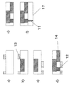
圧電体膜を薄膜とした本発明の圧電体薄膜素子10は少なくとも第1の電極膜、圧電膜、第2の電極膜を含む圧電体薄膜素子であって、詳細を図7で説明する。図7は、圧電体薄膜素子の断面図である。図中で、6は第1の電極、7は圧電膜、8は第2の電極である。圧電体薄膜素子10の断面形状は矩形で表示されているが、台形や逆台形でもよい。図示した圧電体薄膜素子10は基板5上に形成されており、第1の電極膜6が下部電極、第2の電極膜8が上部電極となっている。電極の上下関係はこれに限定されず、第1の電極膜6が上部電極となる構成をとることもできる。この理由はデバイス化の際の製造方法によるものであり、どちらでも本発明の効果を得る事が出来る。また基板5と下部電極膜16の間にバッファー層9があっても良い。
本発明の圧電膜7は、一般式ABO3で構成され、Aの主成分がPbで、Bの主成分がNb、Mg,Zn,Sc,Cd,Ni,Mn,Co,Yb,In,Feの内の少なくとも2種類の元素とTiとを含むペロブスカイト型構造の酸化物材料からなる。好ましい具体例としては、以下の各酸化物材料を挙げることができる。
(1)(Pbk、αl)x(Mgm、Nbn、Tio、βp)yO3
(式中、1≦x/y<1.5、k+l=1、0.7≦k≦1、0≦l≦0.3、m+n+o+p=1、0.1<m<0.3、0.3<n<0.5、0.2<o<0.4、0≦p<0.3を満たし、且つαがLa、Ca、Ba、Sr、Bi、およびSbから選択されるいずれかの1種の元素を含み、βがSc、In、Yb、Ni、Ta、Co、W、Fe、およびSnから選択されるいずれか1種の元素を含む。)で表されるマグネシウム酸ニオブ酸チタン酸を主成分とする酸化物材料。
(2)(Pbk、αl)x(Scm、Nbn、Tio、βp)yO3
(式中、1≦x/y<1.5、k+l=1、0.7≦k≦1、0≦l≦0.3、m+n+o+p=1、0.1<m<0.4、0.1<n<0.4、0.3<o<0.5、0≦p<0.3を満たし、且つαがLa、Ca、Ba、Sr、Bi、およびSbから選択されるいずれかの1種の元素を含み、βがTa、In、Yb、Mg、Ni、Co、W、Fe、およびSnから選択されるいずれか1種の元素を含む。)で表されるスカンジウム酸ニオブ酸チタン酸を主成分とする酸化物材料。
(3)(Pbk、αl)x(Znm、Nbn、Tio、βp)yO3
(式中、1≦x/y<1.5、k+l=1、0.7≦k≦1、0≦l≦0.3、m+n+o+p=1、0.2<m<0.4、0.5<n<0.7、0.05<o<0.2、0≦p<0.3を満たし、且つαがLa、Ca、Ba、Sr、Bi、およびSbから選択されるいずれかの1種の元素を含み、βがSc、In、Yb、Ni、Ta、Co、W、Fe、Sn、およびMgから選択されるいずれか1種の元素を含み。)で表される亜鉛酸ニオブ酸チタン酸を主成分とする酸化物材料。
(1)例えば{110}非対称面の極点測定をした際に、中心から約45°の傾きを表す同じ半径位置に8回対称や12回対称のパターンが得られる結晶。
(2)例えば{110}非対称面の極点測定をした際に、パターンがスポットではなく楕円である結晶。
同様に本発明では、例えば単斜晶と正方晶、単斜晶と菱面体晶、正方晶と菱面体晶、そのすべてなどの複数結晶相が混在(混相)する場合や、双晶や等に起因する結晶が混在する場合や、転位や欠陥等がある場合も、広義に単結晶および1軸配向結晶とみなす。
Qy(004)>Qy(204)、もしくはQy(004)<Qy(204)。
すなわち、(004)逆格子点のy軸方向の大きさ Qy(004)と、(204)逆格子点のx軸方向の大きさ Qx(204)との関係が Qy(004)<2Qx(204)となるような逆格子点が得られる。この際、Qy(004)>Qy(204)、かつ、 Qy(004)<Qy(204)となるような2つの(204)逆格子点が現れても構わない。この2つの逆格子は双晶の関係にあると思われる。
Qy(004)>Qy(204)、もしくはQy(004)<Qy(204)。
すなわち、(004)逆格子点のy軸方向の大きさQy(004)と、(204)のx軸方向の大きさQx(204)との関係が Qy(004)≒2Qx(204)となるような逆格子点が得られる。この際、Qy(004)>Qy(204)、かつ、Qy(004)<Qy(204)となるような2つの(204)逆格子点が現れても構わない。この2つの逆格子は双晶の関係にあると思われる。
本発明における圧電膜の形成方法は特に限定されないが、10μm以下の薄膜では通常、ゾルゲル法、水熱合成法、ガスデポジション法、電気泳動法等の薄膜形成法を用いることができる。さらにはスパッタリング法、化学気相成長法(CVD法)、有機金属気相成長法(MOCVD法)、イオンビームデポジション法、分子線エピタキシー法、レーザーアブレーション法等の薄膜形成法も用いることができる。これらの薄膜形成法では、基板や下部電極からのエピタキシャル成長を用いた圧電膜の形成が可能となる。
本発明の圧電膜素子の第1の電極(電極膜)又は第2の電極(電極膜)は、前述の圧電膜と良好な密着性を有し、かつ導電性の高い材料が好ましい。すなわち、上部電極膜又は下部電極膜の比抵抗を10-7〜10-2Ω・cmとすることのできる材料からなることが好ましい。このような材料は一般的に金属であることが多いが、例えば、Au、Ag、CuやRu、Rh、Pd、Os、Ir、PtなどのPt族の金属を電極材料として用いることが好ましい。また上記材料を含む銀ペーストやはんだなどの合金材料も高い導電性を有し、好ましく用いることができる。また、例えばIrO(酸化イリジウム)、SRO(ルテニウム酸ストロンチウム)、ITO(導電性酸化スズ)、BPO(鉛酸バリウム)などの導電性酸化物材料も電極材料として好ましい。また、電極膜は1層構成でもよく、多層構成でもよい。例えば基板との密着性を上げる為Pt/Tiのような構成としても良いし、基板やバッファー層からエピタキシャル成長をするために、SRO/LNO(ニッケル酸ランタン)のような構成としても良い。
次に、本発明の液体吐出ヘッドについて説明する。
次に本発明の液体吐出ヘッドの製造方法について説明する。本発明の液体吐出ヘッドの製造方法は、少なくとも、次の工程を有する。
(1)吐出口を形成する工程。
(2)吐出口と個別液室を連通する連通孔を形成する工程。
(3)個別液室を形成する工程。
(4)個別液室に連通する共通液室を形成する工程。
(5)個別液室に振動を付与する振動板を形成する工程。
(6)個別液室の外部に設けられた振動板に振動を付与するための本発明の圧電体薄膜素子を製造する工程。
本発明の圧電膜素子の圧電特性の評価はユニモルフ型カンチレバー方式を用いたd31測定法によりおこなった。測定方法・構成概略を図18、図19及び図20に示す。基板5上に下部電極膜16、圧電膜7、上部電極膜18の順で構成された圧電膜素子10は、クランプ冶具502により片側が固定されたユニモルフ型カンチレバーの構成となっている。クランプ冶具502の上側部分502-aは、導電性材料で構成されており、圧電膜7の下部電極膜16と電気的に接触されており、交流電源503の出力端子の一方(不図示)に電気ケーブル504-aに繋がっている。交流電源503の出力端子のもう一方(不図示)は電気ケーブル504-bを通じ上部電極膜18に繋がっており、圧電膜7に交流電圧を印加できる構成となっている。
式1中には、下部電極膜、上部電極膜、その他バッファ層などの物性値項が入っていないが、基板厚さhsがそれらの厚さに対して、充分薄い時それらの層の物性値・膜厚は無視でき、式1は実用上充分な近似式となっている。

実施例1の圧電体薄膜素子の製作手順は以下の通りである。
実施例2の圧電体薄膜素子の製作手順は以下の通りである。
Si{100}基板表面をフッ酸処理した後、バッファー層としてYがドープされたZrO2膜をスパッタリング法で基板温度800℃で100nm成膜し、続いてCeO2膜を基板温度800℃で60nm成膜した。どちらも<100>配向の単結晶膜であった。更にこの上に下部電極膜としてスパッタリング法によりLaNiO3(LNO)膜を100nm厚で基板温度850℃で成膜した。さらにこのLNO膜上にSrRuO3(SRO)膜を基板温度600℃で200nm成膜し下部電極膜等を有する基板を得た。電極膜もSRO膜も<100>配向の単結晶膜であった。
Pb(thd)2:ビス(ヘキサメチルアセチルアセトネート)鉛。
Zn (C5H7H2)2:ビス(アセチルアセトネート)亜鉛。
NbC3H7(C2H5)4:プロピルテトラエチルニオブ。
Ti(C3H7O)4:テトライソプロポキシチタン。
比較例1の圧電体薄膜素子の製作手順は以下の通りである。
比較例1の圧電体薄膜素子の製作手順は以下の通りである。
次に実施例1と比較例1の液体吐出ヘッドを以下の手順で作製した。
6 第1の電極膜
7 圧電膜
8 第2の電極膜
9 バッファー層
10 圧電体薄膜素子
11 吐出口
12 連通孔
13 個別液室
14 共通液室
15 振動板
17 吐出口がある基板表面
19 バッファー層
Claims (10)
- ABO3で構成され、Aの主成分がPbで、Bの主成分がNb、Mg,Zn,Sc,Cd,Ni,Mn,Co,Yb,In,Feの内の少なくとも2種類の元素と、Tiと、であるペロブスカイト型構造の酸化物からなる圧電体であって、
菱面体晶及び単斜晶の内いずれかと、正方晶と、を有する結晶相を含み、
正方晶のa−ドメインおよびc−ドメインを少なくとも有する1軸配向又は単結晶であり、
前記a−ドメインおよびc−ドメインの少なくとも一部が(N0N)面(Nは整数)を双晶面とする双晶の鏡像関係にあり、
1μm以上10μm以下の範囲にある厚さを有する膜として形成されている
ことを特徴とする圧電体。 - 前記酸化物が、
(Pbk、αl)x(Mgm、Nbn、Tio、βp)yO3
(式中、1≦x/y<1.5、k+l=1、0.7≦k≦1、0≦l≦0.3、m+n+o+p=1、0.1<m<0.3、0.3<n<0.5、0.2<o<0.4、0≦p<0.3を満たし、且つαがLa、Ca、Ba、Sr、Bi、およびSbから選択されるいずれかの1種の元素であり、βがSc、In、Yb、Ni、Ta、Co、W、Fe、およびSnから選択されるいずれか1種の元素である。)で表される請求項1に記載の圧電体。 - 前記酸化物が、
(Pbk、αl)x(Scm、Nbn、Tio、βp)yO3
(式中、1≦x/y<1.5、k+l=1、0.7≦k≦1、0≦l≦0.3、m+n+o+p=1、0.1<m<0.4、0.1<n<0.4、0.3<o<0.5、0≦p<0.3を満たし、且つαがLa、Ca、Ba、Sr、Bi、およびSbから選択されるいずれかの1種の元素であり、βがTa、In、Yb、Mg、Ni、Co、W、Fe、およびSnから選択されるいずれか1種の元素である。)で表される請求項1に記載の圧電体。 - 前記酸化物が、
(Pbk、αl)x(Znm、Nbn、Tio、βp)yO3
(式中、1≦x/y<1.5、k+l=1、0.7≦k≦1、0≦l≦0.3、m+n+o+p=1、0.2<m<0.4、0.5<n<0.7、0.05<o<0.2、0≦p<0.3を満たし、且つαがLa、Ca、Ba、Sr、Bi、およびSbから選択されるいずれかの1種の元素であり、βがSc、In、Yb、Ni、Ta、Co、W、Fe、Sn、およびMgから選択されるいずれか1種の元素である。)で表される請求項1に記載の圧電体。 - 基板上に、第1の電極膜、圧電膜及び第2の電極膜を有する圧電体素子であって、
前記圧電膜は請求項1乃至4のいずれか1項に記載の圧電体からなり、前記第1の電極膜及び前記第2の電極膜により前記圧電膜の膜厚方向に電界を印加可能であることを特徴とする圧電体素子。 - 前記圧電膜が<100>配向である請求項5に記載の圧電体素子。
- 前記第1の電極膜が少なくとも<100>配向したペロブスカイト型構造の酸化物を含む請求項5または6に記載の圧電体素子。
- 前記基板として、表面が(100)面であるSiからなる部分を有し、前記Siからなる部分上にバッファー層を有する基板を用いる請求項5乃至7のいずれか1項に記載の圧電体素子。
- 吐出口と、該吐出口から液体を吐出するための圧電体素子と、を備える液体吐出ヘッドにおいて、
前記圧電体素子が請求項5乃至8のいずれか1項に記載の圧電体素子であることを特徴とする液体吐出ヘッド。 - 請求項9記載の液体吐出ヘッドを有することを特徴とする液体吐出装置。
Priority Applications (6)
| Application Number | Priority Date | Filing Date | Title |
|---|---|---|---|
| JP2006196114A JP5300184B2 (ja) | 2006-07-18 | 2006-07-18 | 圧電体、圧電体素子、圧電体素子を用いた液体吐出ヘッド及び液体吐出装置 |
| US12/301,567 US7948154B2 (en) | 2006-07-18 | 2007-07-13 | Piezoelectric substance, piezoelectric element, and liquid discharge head and liquid discharge apparatus using piezoelectric element |
| EP07791121.2A EP2044245B1 (en) | 2006-07-18 | 2007-07-13 | Piezoelectric substance, piezoelectric element, and liquid discharge head and liquid discharge apparatus using piezoelectric element |
| CN2007800269868A CN101490316B (zh) | 2006-07-18 | 2007-07-13 | 压电物质、压电元件及使用压电元件的液体排出头和液体排出设备 |
| PCT/JP2007/064384 WO2008010583A1 (en) | 2006-07-18 | 2007-07-13 | Piezoelectric substance, piezoelectric element, and liquid discharge head and liquid discharge apparatus using piezoelectric element |
| KR1020097003264A KR101113490B1 (ko) | 2006-07-18 | 2007-07-13 | 압전체, 압전체 소자, 및 압전체 소자를 이용한 액체 토출 헤드 및 액체 토출 장치 |
Applications Claiming Priority (1)
| Application Number | Priority Date | Filing Date | Title |
|---|---|---|---|
| JP2006196114A JP5300184B2 (ja) | 2006-07-18 | 2006-07-18 | 圧電体、圧電体素子、圧電体素子を用いた液体吐出ヘッド及び液体吐出装置 |
Publications (3)
| Publication Number | Publication Date |
|---|---|
| JP2008024532A JP2008024532A (ja) | 2008-02-07 |
| JP2008024532A5 JP2008024532A5 (ja) | 2009-09-17 |
| JP5300184B2 true JP5300184B2 (ja) | 2013-09-25 |
Family
ID=38956914
Family Applications (1)
| Application Number | Title | Priority Date | Filing Date |
|---|---|---|---|
| JP2006196114A Expired - Fee Related JP5300184B2 (ja) | 2006-07-18 | 2006-07-18 | 圧電体、圧電体素子、圧電体素子を用いた液体吐出ヘッド及び液体吐出装置 |
Country Status (6)
| Country | Link |
|---|---|
| US (1) | US7948154B2 (ja) |
| EP (1) | EP2044245B1 (ja) |
| JP (1) | JP5300184B2 (ja) |
| KR (1) | KR101113490B1 (ja) |
| CN (1) | CN101490316B (ja) |
| WO (1) | WO2008010583A1 (ja) |
Cited By (1)
| Publication number | Priority date | Publication date | Assignee | Title |
|---|---|---|---|---|
| US9956774B2 (en) | 2015-12-17 | 2018-05-01 | Ricoh Company, Ltd. | Electromechanical transducer element, liquid discharge head, liquid discharge device, method for producing electromechanical transducer film, and method for producing liquid discharge head |
Families Citing this family (19)
| Publication number | Priority date | Publication date | Assignee | Title |
|---|---|---|---|---|
| JP5355148B2 (ja) * | 2008-03-19 | 2013-11-27 | キヤノン株式会社 | 圧電材料 |
| US8894765B1 (en) * | 2009-11-13 | 2014-11-25 | Trs Technologies, Inc. | High polarization energy storage materials using oriented single crystals |
| JPWO2011077667A1 (ja) * | 2009-12-24 | 2013-05-02 | コニカミノルタホールディングス株式会社 | 圧電素子及びその製造方法 |
| JP5854183B2 (ja) * | 2010-03-02 | 2016-02-09 | セイコーエプソン株式会社 | 液体噴射ヘッド、液体噴射装置、圧電素子、超音波センサー及び赤外センサー |
| KR101145667B1 (ko) * | 2010-03-23 | 2012-05-24 | 전자부품연구원 | 산처리 과정을 포함하는 강유전체 박막 형성방법 |
| JP5743059B2 (ja) * | 2011-01-19 | 2015-07-01 | セイコーエプソン株式会社 | 液体噴射ヘッド、液体噴射装置、圧電素子、超音波センサー及び赤外線センサー |
| CN102856177B (zh) * | 2011-06-27 | 2015-01-28 | 中芯国际集成电路制造(北京)有限公司 | 半导体器件和用于制造半导体器件的方法 |
| EP2769421B1 (en) * | 2011-10-18 | 2017-04-05 | Dalhousie University | Piezoelectric materials and methods of property control |
| JP5808262B2 (ja) * | 2012-01-23 | 2015-11-10 | 株式会社サイオクス | 圧電体素子及び圧電体デバイス |
| CN104419895B (zh) * | 2013-09-09 | 2016-11-16 | 中国科学院上海硅酸盐研究所 | 低温下制备具有高度(001)择优取向的钌酸锶薄膜的方法 |
| JP6273829B2 (ja) | 2013-09-13 | 2018-02-07 | 株式会社リコー | 電気機械変換素子とその製造方法、及び電気機械変換素子を有する液滴吐出ヘッド、液滴吐出ヘッドを有する液滴吐出装置 |
| JP6478023B2 (ja) | 2014-03-18 | 2019-03-06 | セイコーエプソン株式会社 | 圧電素子、圧電アクチュエーター装置、液体噴射ヘッド、液体噴射装置及び超音波測定装置 |
| EP3612210A4 (en) | 2017-04-19 | 2021-01-27 | Board Of Regents, The University Of Texas System | IMMUNE CELLS EXPRESSING MODIFIED ANTIGEN RECEPTORS |
| CN107093664B (zh) * | 2017-04-19 | 2019-05-14 | 北京大学 | 一种周期性正交极化的大应变压电陶瓷致动器及制备方法 |
| CN108597875B (zh) * | 2018-04-03 | 2020-10-30 | 湘潭大学 | 一种透明柔性全氧化物异质外延铁电薄膜及其制备方法 |
| JP7298159B2 (ja) * | 2019-01-11 | 2023-06-27 | Tdk株式会社 | 圧電薄膜、圧電薄膜素子、圧電アクチュエータ、圧電センサ、ヘッドアセンブリ、ヘッドスタックアセンブリ、ハードディスクドライブ、プリンタヘッド、及びインクジェットプリンタ装置 |
| CN110590356B (zh) * | 2019-09-20 | 2021-09-10 | 清华大学深圳国际研究生院 | 钛酸锌陶瓷前驱体浆料和3d打印制备钛酸锌陶瓷的方法 |
| CN110588178B (zh) * | 2019-09-30 | 2021-05-14 | 西安交通大学 | 一种高密度压电打印头的集成制造方法 |
| JPWO2022153800A1 (ja) * | 2021-01-12 | 2022-07-21 |
Family Cites Families (26)
| Publication number | Priority date | Publication date | Assignee | Title |
|---|---|---|---|---|
| JP3104550B2 (ja) | 1994-10-17 | 2000-10-30 | 松下電器産業株式会社 | 圧電アクチュエータおよびその製造方法 |
| JP3397538B2 (ja) | 1995-09-14 | 2003-04-14 | 株式会社東芝 | 酸化物圧電単結晶の製造方法 |
| US5804907A (en) * | 1997-01-28 | 1998-09-08 | The Penn State Research Foundation | High strain actuator using ferroelectric single crystal |
| JP4327942B2 (ja) * | 1999-05-20 | 2009-09-09 | Tdk株式会社 | 薄膜圧電素子 |
| JP4516166B2 (ja) * | 1999-09-07 | 2010-08-04 | セイコーエプソン株式会社 | インクジェット式記録ヘッドの製造方法 |
| JP3796394B2 (ja) * | 2000-06-21 | 2006-07-12 | キヤノン株式会社 | 圧電素子の製造方法および液体噴射記録ヘッドの製造方法 |
| US6517737B2 (en) * | 2001-03-02 | 2003-02-11 | Lucent Technologies Inc. | Ceramic piezoelectric and devices using the piezoelectric |
| JP3828116B2 (ja) * | 2003-01-31 | 2006-10-04 | キヤノン株式会社 | 圧電体素子 |
| ATE537568T1 (de) * | 2003-01-31 | 2011-12-15 | Canon Kk | Piezoelektrisches element |
| JP4776154B2 (ja) * | 2003-09-03 | 2011-09-21 | キヤノン株式会社 | 圧電体素子、インクジェット記録ヘッド、圧電体素子の製造方法 |
| JP2005093133A (ja) * | 2003-09-12 | 2005-04-07 | Tomoshi Wada | 強誘電体結晶材料及びその製造方法 |
| JP4717344B2 (ja) * | 2003-12-10 | 2011-07-06 | キヤノン株式会社 | 誘電体薄膜素子、圧電アクチュエータおよび液体吐出ヘッド |
| US7998362B2 (en) * | 2005-08-23 | 2011-08-16 | Canon Kabushiki Kaisha | Piezoelectric substance, piezoelectric element, liquid discharge head using piezoelectric element, liquid discharge apparatus, and production method of piezoelectric element |
| US7521845B2 (en) * | 2005-08-23 | 2009-04-21 | Canon Kabushiki Kaisha | Piezoelectric substance, piezoelectric element, liquid discharge head using piezoelectric element, and liquid discharge apparatus |
| US7591543B2 (en) * | 2005-08-23 | 2009-09-22 | Canon Kabushiki Kaisha | Piezoelectric member, piezoelectric member element, liquid discharge head in use thereof, liquid discharge apparatus and method of manufacturing piezoelectric member |
| US7528530B2 (en) * | 2005-08-23 | 2009-05-05 | Canon Kabushiki Kaisha | Piezoelectric substance, piezoelectric substance element, liquid discharge head, liquid discharge device and method for producing piezoelectric substance |
| US20070046153A1 (en) * | 2005-08-23 | 2007-03-01 | Canon Kabushiki Kaisha | Piezoelectric substrate, piezoelectric element, liquid discharge head and liquid discharge apparatus |
| WO2007023985A1 (ja) * | 2005-08-23 | 2007-03-01 | Canon Kabushiki Kaisha | 圧電体素子、それを用いた液体吐出ヘッド、および液体吐出装置 |
| US8142678B2 (en) * | 2005-08-23 | 2012-03-27 | Canon Kabushiki Kaisha | Perovskite type oxide material, piezoelectric element, liquid discharge head and liquid discharge apparatus using the same, and method of producing perovskite type oxide material |
| JP5041765B2 (ja) * | 2005-09-05 | 2012-10-03 | キヤノン株式会社 | エピタキシャル酸化物膜、圧電膜、圧電膜素子、圧電膜素子を用いた液体吐出ヘッド及び液体吐出装置 |
| US7759845B2 (en) * | 2006-03-10 | 2010-07-20 | Canon Kabushiki Kaisha | Piezoelectric substance element, liquid discharge head utilizing the same and optical element |
| JP2008004781A (ja) * | 2006-06-23 | 2008-01-10 | Fujifilm Corp | 圧電膜、圧電素子、インクジェット式記録ヘッド、及びインクジェット式記録装置 |
| US7874648B2 (en) * | 2006-07-14 | 2011-01-25 | Canon Kabushiki Kaisha | Manufacturing method for piezoelectric body, piezoelectric element, and liquid discharge head |
| US7874649B2 (en) * | 2006-07-14 | 2011-01-25 | Canon Kabushiki Kaisha | Piezoelectric element, ink jet head and producing method for piezoelectric element |
| US7984977B2 (en) * | 2006-07-14 | 2011-07-26 | Canon Kabushiki Kaisha | Piezoelectric element, manufacturing method for piezoelectric body, and liquid jet head |
| JP5307986B2 (ja) * | 2007-05-07 | 2013-10-02 | 富士フイルム株式会社 | 圧電素子とその製造方法、及び液体吐出装置 |
-
2006
- 2006-07-18 JP JP2006196114A patent/JP5300184B2/ja not_active Expired - Fee Related
-
2007
- 2007-07-13 WO PCT/JP2007/064384 patent/WO2008010583A1/en active Application Filing
- 2007-07-13 US US12/301,567 patent/US7948154B2/en not_active Expired - Fee Related
- 2007-07-13 EP EP07791121.2A patent/EP2044245B1/en not_active Expired - Fee Related
- 2007-07-13 KR KR1020097003264A patent/KR101113490B1/ko not_active IP Right Cessation
- 2007-07-13 CN CN2007800269868A patent/CN101490316B/zh not_active Expired - Fee Related
Cited By (1)
| Publication number | Priority date | Publication date | Assignee | Title |
|---|---|---|---|---|
| US9956774B2 (en) | 2015-12-17 | 2018-05-01 | Ricoh Company, Ltd. | Electromechanical transducer element, liquid discharge head, liquid discharge device, method for producing electromechanical transducer film, and method for producing liquid discharge head |
Also Published As
| Publication number | Publication date |
|---|---|
| CN101490316B (zh) | 2013-03-06 |
| JP2008024532A (ja) | 2008-02-07 |
| KR20090040440A (ko) | 2009-04-24 |
| WO2008010583A1 (en) | 2008-01-24 |
| EP2044245A4 (en) | 2012-09-12 |
| EP2044245B1 (en) | 2016-02-10 |
| CN101490316A (zh) | 2009-07-22 |
| KR101113490B1 (ko) | 2012-03-13 |
| EP2044245A1 (en) | 2009-04-08 |
| US7948154B2 (en) | 2011-05-24 |
| US20090273257A1 (en) | 2009-11-05 |
Similar Documents
| Publication | Publication Date | Title |
|---|---|---|
| JP5300184B2 (ja) | 圧電体、圧電体素子、圧電体素子を用いた液体吐出ヘッド及び液体吐出装置 | |
| JP5041765B2 (ja) | エピタキシャル酸化物膜、圧電膜、圧電膜素子、圧電膜素子を用いた液体吐出ヘッド及び液体吐出装置 | |
| JP5127268B2 (ja) | 圧電体、圧電体素子、圧電体素子を用いた液体吐出ヘッド及び液体吐出装置 | |
| JP5241087B2 (ja) | 圧電体、圧電素子、圧電素子を用いた液体吐出ヘッド、液体吐出装置及び圧電素子の製造方法 | |
| JP5164052B2 (ja) | 圧電体素子、液体吐出ヘッド及び液体吐出装置 | |
| US7521845B2 (en) | Piezoelectric substance, piezoelectric element, liquid discharge head using piezoelectric element, and liquid discharge apparatus | |
| JP5241086B2 (ja) | 圧電体、圧電素子、圧電素子を用いた液体吐出ヘッドおよび液体吐出装置 | |
| JP5311775B2 (ja) | 圧電体素子、インクジェットヘッド及び圧電体素子の製造方法 | |
| JP2010067756A (ja) | 圧電体膜、圧電素子、及び液体吐出装置 | |
| JP3828116B2 (ja) | 圧電体素子 | |
| JP2007112069A (ja) | 液体吐出ヘッド | |
| JP5131674B2 (ja) | 圧電体とその製造方法、圧電素子とそれを用いた液体吐出ヘッド及び液体吐出装置 | |
| JP4875827B2 (ja) | 圧電薄膜及びその製造方法、並びにその圧電薄膜を備えた圧電素子、並びにその圧電素子を用いたインクジェットヘッド、並びにそのインクジェットヘッドを備えたインクジェット式記録装置 | |
| JP3907628B2 (ja) | 圧電アクチュエーターおよびその製造方法ならびに液体吐出ヘッド | |
| JP2009094139A (ja) | 圧電アクチュエータ及びそれを用いた液体吐出ヘッド | |
| JP5398131B2 (ja) | 圧電体素子、圧電体の製造方法及び液体噴射ヘッド | |
| JP2007084424A (ja) | ペブロスカイト型酸化物、これを用いた圧電素子、液体吐出ヘッド、液体吐出装置及びペブロスカイト型酸化物の製造方法 | |
| JP2007088445A (ja) | 圧電体、圧電素子、液体吐出ヘッド、液体吐出装置及び圧電体の製造方法 | |
| JP2006173646A (ja) | 強誘電体薄膜素子、圧電アクチュエーター、液体吐出ヘッド |
Legal Events
| Date | Code | Title | Description |
|---|---|---|---|
| A711 | Notification of change in applicant |
Free format text: JAPANESE INTERMEDIATE CODE: A711 Effective date: 20090209 |
|
| A521 | Request for written amendment filed |
Free format text: JAPANESE INTERMEDIATE CODE: A821 Effective date: 20090209 |
|
| A621 | Written request for application examination |
Free format text: JAPANESE INTERMEDIATE CODE: A621 Effective date: 20090721 |
|
| A521 | Request for written amendment filed |
Free format text: JAPANESE INTERMEDIATE CODE: A523 Effective date: 20090730 |
|
| A131 | Notification of reasons for refusal |
Free format text: JAPANESE INTERMEDIATE CODE: A131 Effective date: 20120626 |
|
| A521 | Request for written amendment filed |
Free format text: JAPANESE INTERMEDIATE CODE: A523 Effective date: 20120823 |
|
| A131 | Notification of reasons for refusal |
Free format text: JAPANESE INTERMEDIATE CODE: A131 Effective date: 20121218 |
|
| A521 | Request for written amendment filed |
Free format text: JAPANESE INTERMEDIATE CODE: A523 Effective date: 20130218 |
|
| TRDD | Decision of grant or rejection written | ||
| A01 | Written decision to grant a patent or to grant a registration (utility model) |
Free format text: JAPANESE INTERMEDIATE CODE: A01 Effective date: 20130611 |
|
| A61 | First payment of annual fees (during grant procedure) |
Free format text: JAPANESE INTERMEDIATE CODE: A61 Effective date: 20130618 |
|
| R151 | Written notification of patent or utility model registration |
Ref document number: 5300184 Country of ref document: JP Free format text: JAPANESE INTERMEDIATE CODE: R151 |
|
| LAPS | Cancellation because of no payment of annual fees |