JP5259336B2 - 半導体装置及び半導体装置の製造方法 - Google Patents
半導体装置及び半導体装置の製造方法 Download PDFInfo
- Publication number
- JP5259336B2 JP5259336B2 JP2008273141A JP2008273141A JP5259336B2 JP 5259336 B2 JP5259336 B2 JP 5259336B2 JP 2008273141 A JP2008273141 A JP 2008273141A JP 2008273141 A JP2008273141 A JP 2008273141A JP 5259336 B2 JP5259336 B2 JP 5259336B2
- Authority
- JP
- Japan
- Prior art keywords
- semiconductor device
- heat sink
- manufacturing
- cutting
- wiring board
- Prior art date
- Legal status (The legal status is an assumption and is not a legal conclusion. Google has not performed a legal analysis and makes no representation as to the accuracy of the status listed.)
- Expired - Fee Related
Links
Images


Classifications
-
- H—ELECTRICITY
- H10—SEMICONDUCTOR DEVICES; ELECTRIC SOLID-STATE DEVICES NOT OTHERWISE PROVIDED FOR
- H10W—GENERIC PACKAGES, INTERCONNECTIONS, CONNECTORS OR OTHER CONSTRUCTIONAL DETAILS OF DEVICES COVERED BY CLASS H10
- H10W74/00—Encapsulations, e.g. protective coatings
- H10W74/01—Manufacture or treatment
- H10W74/014—Manufacture or treatment using batch processing
-
- H—ELECTRICITY
- H10—SEMICONDUCTOR DEVICES; ELECTRIC SOLID-STATE DEVICES NOT OTHERWISE PROVIDED FOR
- H10W—GENERIC PACKAGES, INTERCONNECTIONS, CONNECTORS OR OTHER CONSTRUCTIONAL DETAILS OF DEVICES COVERED BY CLASS H10
- H10W40/00—Arrangements for thermal protection or thermal control
- H10W40/70—Fillings or auxiliary members in containers or in encapsulations for thermal protection or control
- H10W40/77—Auxiliary members characterised by their shape
- H10W40/778—Auxiliary members characterised by their shape in encapsulations
-
- H—ELECTRICITY
- H10—SEMICONDUCTOR DEVICES; ELECTRIC SOLID-STATE DEVICES NOT OTHERWISE PROVIDED FOR
- H10W—GENERIC PACKAGES, INTERCONNECTIONS, CONNECTORS OR OTHER CONSTRUCTIONAL DETAILS OF DEVICES COVERED BY CLASS H10
- H10W72/00—Interconnections or connectors in packages
- H10W72/01—Manufacture or treatment
- H10W72/0198—Manufacture or treatment batch processes
-
- H—ELECTRICITY
- H10—SEMICONDUCTOR DEVICES; ELECTRIC SOLID-STATE DEVICES NOT OTHERWISE PROVIDED FOR
- H10W—GENERIC PACKAGES, INTERCONNECTIONS, CONNECTORS OR OTHER CONSTRUCTIONAL DETAILS OF DEVICES COVERED BY CLASS H10
- H10W72/00—Interconnections or connectors in packages
- H10W72/071—Connecting or disconnecting
- H10W72/072—Connecting or disconnecting of bump connectors
- H10W72/07251—Connecting or disconnecting of bump connectors characterised by changes in properties of the bump connectors during connecting
-
- H—ELECTRICITY
- H10—SEMICONDUCTOR DEVICES; ELECTRIC SOLID-STATE DEVICES NOT OTHERWISE PROVIDED FOR
- H10W—GENERIC PACKAGES, INTERCONNECTIONS, CONNECTORS OR OTHER CONSTRUCTIONAL DETAILS OF DEVICES COVERED BY CLASS H10
- H10W72/00—Interconnections or connectors in packages
- H10W72/20—Bump connectors, e.g. solder bumps or copper pillars; Dummy bumps; Thermal bumps
-
- H—ELECTRICITY
- H10—SEMICONDUCTOR DEVICES; ELECTRIC SOLID-STATE DEVICES NOT OTHERWISE PROVIDED FOR
- H10W—GENERIC PACKAGES, INTERCONNECTIONS, CONNECTORS OR OTHER CONSTRUCTIONAL DETAILS OF DEVICES COVERED BY CLASS H10
- H10W74/00—Encapsulations, e.g. protective coatings
-
- H—ELECTRICITY
- H10—SEMICONDUCTOR DEVICES; ELECTRIC SOLID-STATE DEVICES NOT OTHERWISE PROVIDED FOR
- H10W—GENERIC PACKAGES, INTERCONNECTIONS, CONNECTORS OR OTHER CONSTRUCTIONAL DETAILS OF DEVICES COVERED BY CLASS H10
- H10W74/00—Encapsulations, e.g. protective coatings
- H10W74/10—Encapsulations, e.g. protective coatings characterised by their shape or disposition
- H10W74/111—Encapsulations, e.g. protective coatings characterised by their shape or disposition the semiconductor body being completely enclosed
- H10W74/114—Encapsulations, e.g. protective coatings characterised by their shape or disposition the semiconductor body being completely enclosed by a substrate and the encapsulations
- H10W74/117—Encapsulations, e.g. protective coatings characterised by their shape or disposition the semiconductor body being completely enclosed by a substrate and the encapsulations the substrate having spherical bumps for external connection
-
- H—ELECTRICITY
- H10—SEMICONDUCTOR DEVICES; ELECTRIC SOLID-STATE DEVICES NOT OTHERWISE PROVIDED FOR
- H10W—GENERIC PACKAGES, INTERCONNECTIONS, CONNECTORS OR OTHER CONSTRUCTIONAL DETAILS OF DEVICES COVERED BY CLASS H10
- H10W90/00—Package configurations
- H10W90/701—Package configurations characterised by the relative positions of pads or connectors relative to package parts
- H10W90/721—Package configurations characterised by the relative positions of pads or connectors relative to package parts of bump connectors
- H10W90/722—Package configurations characterised by the relative positions of pads or connectors relative to package parts of bump connectors between stacked chips
-
- H—ELECTRICITY
- H10—SEMICONDUCTOR DEVICES; ELECTRIC SOLID-STATE DEVICES NOT OTHERWISE PROVIDED FOR
- H10W—GENERIC PACKAGES, INTERCONNECTIONS, CONNECTORS OR OTHER CONSTRUCTIONAL DETAILS OF DEVICES COVERED BY CLASS H10
- H10W90/00—Package configurations
- H10W90/701—Package configurations characterised by the relative positions of pads or connectors relative to package parts
- H10W90/751—Package configurations characterised by the relative positions of pads or connectors relative to package parts of bond wires
- H10W90/754—Package configurations characterised by the relative positions of pads or connectors relative to package parts of bond wires between a chip and a stacked insulating package substrate, interposer or RDL
Landscapes
- Encapsulation Of And Coatings For Semiconductor Or Solid State Devices (AREA)
- Cooling Or The Like Of Semiconductors Or Solid State Devices (AREA)
Description
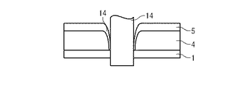
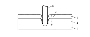
これに対して、上述の発明によれば、放熱板(5)側から削る工程(S51)により、放熱板(5)の少なくとも一部が削られる。この工程において、放熱板(5)が引っ張られる方向には、封止樹脂(4)が設けられている。封止樹脂(4)により、放熱板(5)が押さえられるので、放熱板(5)の変形は抑えられる。また、配線基板(1)側から削る工程(S52)では、放熱板(5)は、全く削られる必要がないか、一部が削られるだけでよい。放熱板(5)において、支えの無い方向に向かって削られる量を少なくすることができる。その結果、バリの発生を抑えることができる。
これに対して、上述の発明によれば、配線基板(1)側から削る工程(S52)により、樹脂封止体(10)の板厚方向における少なくとも一部が、配線基板(1)側から削られる。従って、放熱板(5)側からは、板厚方向における一部を削るだけでよい。放熱板(5)が切断時に引っ張られることもなく、放熱板(5)の変形が抑制される。
以下、図面を参照しつつ、第1の実施形態について説明する。
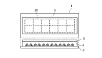
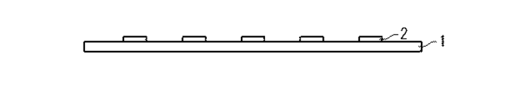
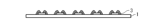
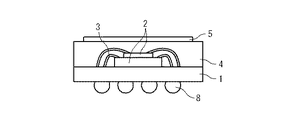
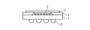
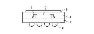
まず、図8Aに示されるように、配線基板1を用意し、配線基板1の主面上に複数の半導体チップ2を搭載する。
続いて、図8Bに示されるように、ワイヤボンディングを行い、複数の半導体チップ2の各々を、ワイヤ3を介して配線基板1に電気的に接続する。
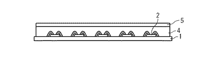
続いて、図8Cに示されるように、放熱板5を半導体チップの上方に、配線基板1の主面と対向するように配置する。
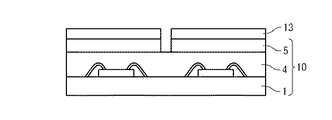
そして、配線基板1と放熱板5との間に、封止樹脂4を供給し、硬化する。これにより、複数の半導体チップ2が封止樹脂4により一括して封止される。
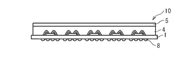
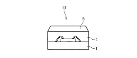
続いて、図8Dに示されるように、配線基板1の裏面に、ボール状電極群8を形成する。これにより、樹脂封止体10が得られる。
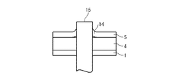
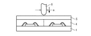
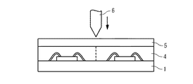
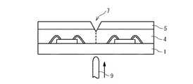
続いて、円盤状のブレードを回転させて樹脂封止体10に当接させ、樹脂封止体10を切断する。
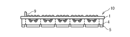
これに対して、本実施形態によれば、放熱板5側から削る工程(S51)により、放熱板5の少なくとも一部が削られる。この工程において、放熱板5が引っ張られる方向には、封止樹脂4が設けられている。封止樹脂4により、放熱板5が押さえられるので、放熱板5の変形は少ない。また、放熱板5側から削る工程(S51)において放熱板5の一部が削られるので、配線基板1側から削る工程(S52)では、放熱板5は、全く削られる必要がないか、一部が削られるだけでよい。従って、放熱板5において、遮るものが無い方向(配線基板1から放熱板1に向かう方向)に向かって削られる量を少なくすることができる。その結果、バリの発生を抑えることができる。
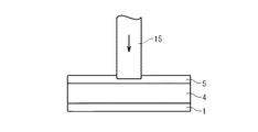
これに対して、本実施形態によれば、配線基板側から削る工程(S52)により、樹脂封止体10の板厚方向における少なくとも一部が、配線基板1側から削られる。従って、放熱板5側から削る工程(S51)では、板厚方向における一部を削るだけでよい。放熱板5に加わる力(引っ張り力)の量を小さくすることができ、バリを抑制することができる。通常バリが発生すると、製品安全性の観点からバリを除去する必要があるが、本発明ではバリの発生が抑制されるため、バリの除去工程が不要となる。そのため、ブレードでの切断工程が2工程となるが、バリ除去工程が不要のため工程数増加とはならない。
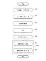
続いて、本発明の第2の実施形態について説明する。図14は、本実施形態に係る半導体装置の製造方法を示すフローチャートである。本実施形態では、第1の実施形態に対して、ボールマウント工程(S40)の順番が異なっている。それ以外の点については、第1の実施形態と同様とすることができるので、詳細な説明は省略する。
続いて、本発明の第3の実施形態について説明する。本実施形態では、既述の実施形態に対して、放熱板5側から削る工程(S51)における動作が工夫されている。その他の点については、既述の実施形態と同様とすることができるので、詳細な説明は省略する。
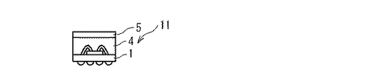
2 半導体チップ
3 ワイヤ
4 封止樹脂
5 放熱板
6 第1のブレード
7 溝
8 ボール電極
9 第2のブレード
10 樹脂封止体
11 半導体装置
12 弾性シート
13 レジストマスク
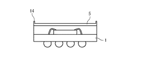
14 バリ
15 ブレード
20 製品エリア
21 単位製品エリア
Claims (11)
- 配線基板の主面上に複数の半導体チップを搭載する工程と、
前記複数の半導体チップの上方に放熱板を配置する工程と、
前記放熱板と前記配線基板との間に封止樹脂を供給して前記複数の半導体チップを封止し、樹脂封止体を作製する工程と、
前記樹脂封止体を切断する工程と、
を具備し、
前記切断する工程は、
前記樹脂封止体を放熱板側から削る工程と、
前記樹脂封止体を前記配線基板側から削る工程とを備え、
前記配線基板側から削る工程は、前記放熱板側から削る工程よりも後に実施され、
前記配線基板側から削る工程により、前記樹脂封止体が切断され、
更に、
前記配線基板側から削る工程及び前記放熱板側から削る工程よりも前に、前記配線基板の裏面にボール状の電極群を実装する工程
を具備する
半導体装置の製造方法。 - 請求項1に記載された半導体装置の製造方法であって、
前記樹脂封止体が前記放熱板側から削る工程により削られる部分の溝幅は、前記配線基板側から削る工程により削られる部分の溝幅よりも、広い
半導体装置の製造方法。 - 請求項1に記載された半導体装置の製造方法であって、
前記放熱板側から削る工程は、第1のブレードにより前記樹脂封止体を削る工程を含む半導体装置の製造方法。 - 請求項3に記載された半導体装置の製造方法であって、
前記第1のブレードは、刃先の形状が先鋭である
半導体装置の製造方法。 - 前記第1のブレードは、刃先の形状が丸くなっていることを特徴とする、請求項3に記載の半導体装置の製造方法。
- 請求項1乃至5のいずれかに記載された半導体装置の製造方法であって、
前記放熱板側から削る工程では、前記放熱板が完全に分断される
半導体装置の製造方法。 - 請求項3に記載された半導体装置の製造方法であって、
前記配線基板側から削る工程は、第2のブレードにより前記樹脂封止体を削る工程を含む
半導体装置の製造方法。 - 請求項7に記載された半導体装置の製造方法であって、
前記第1のブレードは、前記第2のブレードよりも粗い砥粒が配置されていることを特徴とする半導体装置の製造方法。 - 請求項1乃至8のいずれかに記載された半導体装置の製造方法であって、
前記放熱板は、金属製である
半導体装置の製造方法。 - 請求項9に記載された半導体装置の製造方法であって、
前記放熱板は、被膜が表面に施されている
半導体装置の製造方法。 - 配線基板上に搭載された複数の半導体チップと、前記複数の半導体チップの上方に配置された放熱板と、前記配線基板と前記放熱板との間隙に充填された封止樹脂とで、少なくとも構成された樹脂封止体を複数の個片に切断する半導体装置の製造方法であって、
前記樹脂封止体を前記放熱板側から削る工程と、
前記樹脂封止体を前記配線基板側から削る工程と、
を具備する
半導体装置の製造方法。
Priority Applications (4)
| Application Number | Priority Date | Filing Date | Title |
|---|---|---|---|
| JP2008273141A JP5259336B2 (ja) | 2008-10-23 | 2008-10-23 | 半導体装置及び半導体装置の製造方法 |
| US12/588,542 US20100105170A1 (en) | 2008-10-23 | 2009-10-19 | Method for manufacturing a semiconductor device having a heat spreader |
| US12/929,291 US20110104872A1 (en) | 2008-10-23 | 2011-01-12 | Method of manufacturing a semiconductor device having a heat spreader |
| US13/610,460 US20130005090A1 (en) | 2008-10-23 | 2012-09-11 | Method for manufacturing a semiconductor device having a heat spreader |
Applications Claiming Priority (1)
| Application Number | Priority Date | Filing Date | Title |
|---|---|---|---|
| JP2008273141A JP5259336B2 (ja) | 2008-10-23 | 2008-10-23 | 半導体装置及び半導体装置の製造方法 |
Publications (3)
| Publication Number | Publication Date |
|---|---|
| JP2010103297A JP2010103297A (ja) | 2010-05-06 |
| JP2010103297A5 JP2010103297A5 (ja) | 2011-11-17 |
| JP5259336B2 true JP5259336B2 (ja) | 2013-08-07 |
Family
ID=42117912
Family Applications (1)
| Application Number | Title | Priority Date | Filing Date |
|---|---|---|---|
| JP2008273141A Expired - Fee Related JP5259336B2 (ja) | 2008-10-23 | 2008-10-23 | 半導体装置及び半導体装置の製造方法 |
Country Status (2)
| Country | Link |
|---|---|
| US (3) | US20100105170A1 (ja) |
| JP (1) | JP5259336B2 (ja) |
Families Citing this family (2)
| Publication number | Priority date | Publication date | Assignee | Title |
|---|---|---|---|---|
| JP6716403B2 (ja) * | 2016-09-09 | 2020-07-01 | 株式会社ディスコ | 積層ウェーハの加工方法 |
| TWI772160B (zh) | 2021-08-25 | 2022-07-21 | 慧榮科技股份有限公司 | 半導體封裝元件的形成方法 |
Family Cites Families (11)
| Publication number | Priority date | Publication date | Assignee | Title |
|---|---|---|---|---|
| US4904610A (en) * | 1988-01-27 | 1990-02-27 | General Instrument Corporation | Wafer level process for fabricating passivated semiconductor devices |
| JP3514101B2 (ja) * | 1998-01-28 | 2004-03-31 | セイコーエプソン株式会社 | 半導体装置及びその製造方法並びに電子機器 |
| JP3425378B2 (ja) * | 1998-10-21 | 2003-07-14 | 沖電気工業株式会社 | 半導体装置の製造方法 |
| TWI228780B (en) * | 2000-05-11 | 2005-03-01 | Disco Corp | Semiconductor wafer dividing method |
| JP4672201B2 (ja) * | 2001-07-26 | 2011-04-20 | ローム株式会社 | 半導体装置の製造方法 |
| JP3888439B2 (ja) * | 2002-02-25 | 2007-03-07 | セイコーエプソン株式会社 | 半導体装置の製造方法 |
| US6908784B1 (en) * | 2002-03-06 | 2005-06-21 | Micron Technology, Inc. | Method for fabricating encapsulated semiconductor components |
| JP2006114636A (ja) * | 2004-10-13 | 2006-04-27 | Fujitsu Ltd | 半導体装置の製造方法及び半導体装置 |
| JP2008047573A (ja) * | 2006-08-11 | 2008-02-28 | Matsushita Electric Ind Co Ltd | 樹脂封止型半導体装置の製造装置、樹脂封止型半導体装置の製造方法、および樹脂封止型半導体装置 |
| JP2008288285A (ja) * | 2007-05-15 | 2008-11-27 | Sharp Corp | 積層基板の切断方法、半導体装置の製造方法、半導体装置、発光装置及びバックライト装置 |
| US7824962B2 (en) * | 2008-01-29 | 2010-11-02 | Infineon Technologies Ag | Method of integrated circuit fabrication |
-
2008
- 2008-10-23 JP JP2008273141A patent/JP5259336B2/ja not_active Expired - Fee Related
-
2009
- 2009-10-19 US US12/588,542 patent/US20100105170A1/en not_active Abandoned
-
2011
- 2011-01-12 US US12/929,291 patent/US20110104872A1/en not_active Abandoned
-
2012
- 2012-09-11 US US13/610,460 patent/US20130005090A1/en not_active Abandoned
Also Published As
| Publication number | Publication date |
|---|---|
| US20100105170A1 (en) | 2010-04-29 |
| US20130005090A1 (en) | 2013-01-03 |
| US20110104872A1 (en) | 2011-05-05 |
| JP2010103297A (ja) | 2010-05-06 |
Similar Documents
| Publication | Publication Date | Title |
|---|---|---|
| CN109256369B (zh) | 玻璃中介层的制造方法 | |
| US8174117B2 (en) | Semiconductor device and method of manufacturing the same | |
| JP3143888U (ja) | 部品内蔵モジュール | |
| JP5057221B2 (ja) | 放熱部付き金属ベースプリント基板及びその製造方法 | |
| US20070226996A1 (en) | Hybrid integrated circuit device and method of manufacturing the same | |
| JP2011187659A (ja) | 半導体装置及び半導体装置の製造方法 | |
| JP6887326B2 (ja) | 半導体パッケージの形成方法 | |
| JP2005191149A (ja) | 混成集積回路装置の製造方法 | |
| CN110767553A (zh) | 芯片封装的方法、芯片和芯片封装组件 | |
| JP5435428B2 (ja) | 箔状放熱フィンを備えた放熱器及びその形成方法 | |
| CN1310316C (zh) | 混合集成电路装置 | |
| JP5259336B2 (ja) | 半導体装置及び半導体装置の製造方法 | |
| JP2010097963A (ja) | 回路基板及びその製造方法、電子部品モジュール | |
| JP2009064806A (ja) | 回路基板及びその製造方法並びに半導体モジュール | |
| US20050161781A1 (en) | Hybrid integrated circuit device and manufacturing method thereof | |
| CN1677667A (zh) | 混合集成电路装置及其制造方法 | |
| JP4606447B2 (ja) | 中板の金属基板の製造方法。 | |
| JP6899980B1 (ja) | 半導体装置モジュールおよびその製造方法 | |
| JP2006100750A (ja) | 回路装置およびその製造方法 | |
| TWI776768B (zh) | 散熱貼片及薄膜覆晶封裝結構 | |
| JP2003318334A (ja) | 混成集積回路装置 | |
| JP6779088B2 (ja) | 配線基板の製造方法 | |
| JP4498966B2 (ja) | 金属−セラミックス接合基板 | |
| JP2004311691A (ja) | 回路用金属板およびセラミックス回路基板 | |
| CN1771659A (zh) | 声表面波滤波器及其制作方法 |
Legal Events
| Date | Code | Title | Description |
|---|---|---|---|
| A521 | Request for written amendment filed |
Free format text: JAPANESE INTERMEDIATE CODE: A523 Effective date: 20110929 |
|
| A621 | Written request for application examination |
Free format text: JAPANESE INTERMEDIATE CODE: A621 Effective date: 20110929 |
|
| A977 | Report on retrieval |
Free format text: JAPANESE INTERMEDIATE CODE: A971007 Effective date: 20130118 |
|
| A131 | Notification of reasons for refusal |
Free format text: JAPANESE INTERMEDIATE CODE: A131 Effective date: 20130201 |
|
| A521 | Request for written amendment filed |
Free format text: JAPANESE INTERMEDIATE CODE: A523 Effective date: 20130321 |
|
| TRDD | Decision of grant or rejection written | ||
| A01 | Written decision to grant a patent or to grant a registration (utility model) |
Free format text: JAPANESE INTERMEDIATE CODE: A01 Effective date: 20130419 |
|
| A61 | First payment of annual fees (during grant procedure) |
Free format text: JAPANESE INTERMEDIATE CODE: A61 Effective date: 20130424 |
|
| FPAY | Renewal fee payment (event date is renewal date of database) |
Free format text: PAYMENT UNTIL: 20160502 Year of fee payment: 3 |
|
| R150 | Certificate of patent or registration of utility model |
Free format text: JAPANESE INTERMEDIATE CODE: R150 |
|
| S531 | Written request for registration of change of domicile |
Free format text: JAPANESE INTERMEDIATE CODE: R313531 |
|
| R350 | Written notification of registration of transfer |
Free format text: JAPANESE INTERMEDIATE CODE: R350 |
|
| LAPS | Cancellation because of no payment of annual fees |