JP5241168B2 - 電子顕微鏡 - Google Patents
電子顕微鏡 Download PDFInfo
- Publication number
- JP5241168B2 JP5241168B2 JP2007207342A JP2007207342A JP5241168B2 JP 5241168 B2 JP5241168 B2 JP 5241168B2 JP 2007207342 A JP2007207342 A JP 2007207342A JP 2007207342 A JP2007207342 A JP 2007207342A JP 5241168 B2 JP5241168 B2 JP 5241168B2
- Authority
- JP
- Japan
- Prior art keywords
- sample
- potential
- electron microscope
- electrons
- scanning electron
- Prior art date
- Legal status (The legal status is an assumption and is not a legal conclusion. Google has not performed a legal analysis and makes no representation as to the accuracy of the status listed.)
- Expired - Fee Related
Links
Images


Classifications
-
- H—ELECTRICITY
- H01—ELECTRIC ELEMENTS
- H01J—ELECTRIC DISCHARGE TUBES OR DISCHARGE LAMPS
- H01J37/00—Discharge tubes with provision for introducing objects or material to be exposed to the discharge, e.g. for the purpose of examination or processing thereof
- H01J37/02—Details
- H01J37/244—Detectors; Associated components or circuits therefor
-
- H—ELECTRICITY
- H01—ELECTRIC ELEMENTS
- H01J—ELECTRIC DISCHARGE TUBES OR DISCHARGE LAMPS
- H01J37/00—Discharge tubes with provision for introducing objects or material to be exposed to the discharge, e.g. for the purpose of examination or processing thereof
- H01J37/02—Details
- H01J37/21—Means for adjusting the focus
-
- H—ELECTRICITY
- H01—ELECTRIC ELEMENTS
- H01J—ELECTRIC DISCHARGE TUBES OR DISCHARGE LAMPS
- H01J37/00—Discharge tubes with provision for introducing objects or material to be exposed to the discharge, e.g. for the purpose of examination or processing thereof
- H01J37/26—Electron or ion microscopes; Electron or ion diffraction tubes
- H01J37/28—Electron or ion microscopes; Electron or ion diffraction tubes with scanning beams
-
- H—ELECTRICITY
- H01—ELECTRIC ELEMENTS
- H01J—ELECTRIC DISCHARGE TUBES OR DISCHARGE LAMPS
- H01J37/00—Discharge tubes with provision for introducing objects or material to be exposed to the discharge, e.g. for the purpose of examination or processing thereof
- H01J37/30—Electron-beam or ion-beam tubes for localised treatment of objects
- H01J37/304—Controlling tubes by information coming from the objects or from the beam, e.g. correction signals
- H01J37/3045—Object or beam position registration
-
- H—ELECTRICITY
- H01—ELECTRIC ELEMENTS
- H01J—ELECTRIC DISCHARGE TUBES OR DISCHARGE LAMPS
- H01J2237/00—Discharge tubes exposing object to beam, e.g. for analysis treatment, etching, imaging
- H01J2237/245—Detection characterised by the variable being measured
- H01J2237/24564—Measurements of electric or magnetic variables, e.g. voltage, current, frequency
-
- H—ELECTRICITY
- H01—ELECTRIC ELEMENTS
- H01J—ELECTRIC DISCHARGE TUBES OR DISCHARGE LAMPS
- H01J2237/00—Discharge tubes exposing object to beam, e.g. for analysis treatment, etching, imaging
- H01J2237/25—Tubes for localised analysis using electron or ion beams
- H01J2237/2505—Tubes for localised analysis using electron or ion beams characterised by their application
- H01J2237/2594—Measuring electric fields or potentials
-
- H—ELECTRICITY
- H01—ELECTRIC ELEMENTS
- H01J—ELECTRIC DISCHARGE TUBES OR DISCHARGE LAMPS
- H01J2237/00—Discharge tubes exposing object to beam, e.g. for analysis treatment, etching, imaging
- H01J2237/26—Electron or ion microscopes
- H01J2237/28—Scanning microscopes
-
- H—ELECTRICITY
- H01—ELECTRIC ELEMENTS
- H01J—ELECTRIC DISCHARGE TUBES OR DISCHARGE LAMPS
- H01J2237/00—Discharge tubes exposing object to beam, e.g. for analysis treatment, etching, imaging
- H01J2237/26—Electron or ion microscopes
- H01J2237/28—Scanning microscopes
- H01J2237/2813—Scanning microscopes characterised by the application
- H01J2237/2814—Measurement of surface topography
- H01J2237/2816—Length
-
- H—ELECTRICITY
- H01—ELECTRIC ELEMENTS
- H01J—ELECTRIC DISCHARGE TUBES OR DISCHARGE LAMPS
- H01J2237/00—Discharge tubes exposing object to beam, e.g. for analysis treatment, etching, imaging
- H01J2237/30—Electron or ion beam tubes for processing objects
- H01J2237/304—Controlling tubes
- H01J2237/30455—Correction during exposure
- H01J2237/30461—Correction during exposure pre-calculated
Landscapes
- Chemical & Material Sciences (AREA)
- Analytical Chemistry (AREA)
- Testing Or Measuring Of Semiconductors Or The Like (AREA)
Description
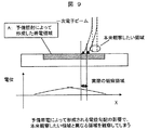
1.電位を測定するステップ
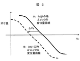
試料に一次電子線が入射しないミラー条件下で、光学的なパラメータ(対物レンズに対する物点ZC,対物レンズの励磁電流Iobj,試料電位Vs=Vr+ΔVs,ブースタ電位Vb)を任意の値に設定し、変位量(検出器上のH軌道の到達点)若しくは、倍率(検出器上のG軌道の到達点)を計測して試料電位を算出する。変位量及び倍率の検出方法を下に示す。
2.装置条件(フォーカス,倍率,観察座標)を自動的に補正するステップ
ウェハが帯電していない場合、フォーカスに必要な対物レンズの励磁電流は一般的に式(1)に示すような関数であらわされる。
ここで、Iobjはウェハが帯電していない時の対物レンズの励磁電流、Fは対物レンズの励磁電流を計算する関数、Vrはウェハに印加されるリターディング電位、Zはウェハの高さである。関数Fは光学シミュレーションあるいは実測により導出できる。通常帯電していないウェハの電位は、ウェハに印加されたリターディング電位と同電位で、式(1)を満たすため、所定のフォーカス制御が可能である。ところがウェハ自身が帯電している場合に必要な対物レンズの励磁電流は式(2)に示すようになるため帯電している場合と帯電していない場合ではフォーカス電流が異なる。
Vsは試料電位でウェハに印加されるリターディング電位Vrと帯電電位ΔVsの和で表せる。
また、Mobjは下式で表せる。
ここで、Schargeは帯電している領域の面積である。
・一次電子線の反射面であるミラー面を試料に近づける。
・ミラー面上での一次電子の拡がりを小さくする。
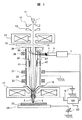
2 等電位面(ミラー面)
3 ミラー電子
11 電界放出陰極
12 引出電極
13 加速電極
14 コンデンサレンズ
15 絞り
17 対物レンズ
18 加速円筒
20 筒状円筒
21 上走査偏向器
22 下走査偏向器
23 試料
24 ホルダー
29 検出器
29b 複数の検出器
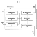
40 演算器
41 分析器
42 対物レンズ制御系
43 ステージ電圧制御系
44 加速電圧制御系
45 第2の演算器
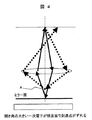
50 参照画像
50a ビーム通過口の画像
50b 構造物(メッシュ)の画像
51 電位測定時の画像
51a ビーム通過口の画像
51b 構造物(メッシュ)の画像
52a,52b,52c 参照画像のビーム通過口の位置
53 電位測定時のビーム通過口位置
54 画像
55 抽出箇所
58 相関曲線
Claims (8)
- 試料に電位を与えるステージと、電子ビームを試料上で走査する偏向器を有する走査電子顕微鏡において、
試料に与える電位を加速電子ビームよりも大きく設定して入射電子を試料直上で反射させる制御装置と、当該反射電子(ミラー電子)の到達位置、もしくは分布、又は電子顕微鏡内の構造物の画像を形成するための電子を検出する検出器を備え、
前記制御装置は、予め求められた前記到達位置、分布、或いは構造物の画像の特徴量と試料電位との関係に基づいて、前記試料の電位を求め、当該求められた試料電位に基づいて、前記偏向器の偏向量の調整を行うことを特徴とする走査型電子顕微鏡。 - 請求項1に示す走査型電子顕微鏡において、
半導体ウェハに電圧を印加する場合、測定した電位に基づいて半導体ウェハに印加する電圧を調整することを特徴とする走査型電子顕微鏡。 - 請求項1又は2において、
前記偏向器と前記電子ビームを集束する対物レンズとの間に前記検出器を配置することを特徴とする走査型電子顕微鏡。 - 請求項3において、
前記検出器は、複数の検出素子が二次元的に配列されていることを特徴とする走査型電子顕微鏡。 - 請求項1から4のいずれかにおいて、
前記試料電位を求める際に、前記電子ビームの開き角を変化させることを特徴とする走査型電子顕微鏡。 - 請求項1から5のいずれかにおいて、
前記試料電位を求める際に、前記試料に印加する電圧に同期して偏向支点を変化させることを特徴とする走査型電子顕微鏡。 - 試料に電位を与えるステージを有する走査電子顕微鏡において、
試料に与える電位を加速電子ビームよりも大きく設定して入射電子を試料直上で反射させる制御装置と、当該反射電子(ミラー電子)の到達位置、もしくは分布、又は電子顕微鏡内の構造物の画像を形成するための電子を検出する検出器を備え、
前記制御装置は、観察を開始する前に当該観察領域について、予め求められた前記到達位置、分布、或いは構造物の画像の特徴量と試料電位との関係に基づいて、前記試料の電位を求め、
当該観察領域内に横方向の電位勾配が発生していた場合、予備帯電を行うことを特徴とする走査型電子顕微鏡。 - 試料に電位を与えるステージを有する走査電子顕微鏡において、
試料に与える電位を加速電子ビームよりも大きく設定して入射電子を試料直上で反射させる制御装置と、当該反射電子(ミラー電子)の到達位置、もしくは分布、又は電子顕微鏡内の構造物の画像を形成するための電子を検出する検出器を備え、
前記制御装置は、観察を開始する前に当該観察領域について、予め求められた前記到達位置、分布、或いは構造物の画像の特徴量と試料電位との関係に基づいて、前記試料の電位を求め、
当該観察領域内に横方向の電位勾配が発生していた場合、
当該横方向の電位勾配による電子ビームの到達点の変化分を補正するよう観察座標を変更することを特徴とする走査型電子顕微鏡。
Priority Applications (3)
| Application Number | Priority Date | Filing Date | Title |
|---|---|---|---|
| JP2007207342A JP5241168B2 (ja) | 2007-08-09 | 2007-08-09 | 電子顕微鏡 |
| US12/188,870 US7989768B2 (en) | 2007-08-09 | 2008-08-08 | Scanning electron microscope |
| US13/190,153 US8481935B2 (en) | 2007-08-09 | 2011-07-25 | Scanning electron microscope |
Applications Claiming Priority (1)
| Application Number | Priority Date | Filing Date | Title |
|---|---|---|---|
| JP2007207342A JP5241168B2 (ja) | 2007-08-09 | 2007-08-09 | 電子顕微鏡 |
Publications (2)
| Publication Number | Publication Date |
|---|---|
| JP2009043936A JP2009043936A (ja) | 2009-02-26 |
| JP5241168B2 true JP5241168B2 (ja) | 2013-07-17 |
Family
ID=40345589
Family Applications (1)
| Application Number | Title | Priority Date | Filing Date |
|---|---|---|---|
| JP2007207342A Expired - Fee Related JP5241168B2 (ja) | 2007-08-09 | 2007-08-09 | 電子顕微鏡 |
Country Status (2)
| Country | Link |
|---|---|
| US (2) | US7989768B2 (ja) |
| JP (1) | JP5241168B2 (ja) |
Families Citing this family (14)
| Publication number | Priority date | Publication date | Assignee | Title |
|---|---|---|---|---|
| JP4969231B2 (ja) | 2006-12-19 | 2012-07-04 | 株式会社日立ハイテクノロジーズ | 試料電位情報検出方法及び荷電粒子線装置 |
| JP5075431B2 (ja) * | 2007-02-28 | 2012-11-21 | 株式会社日立ハイテクノロジーズ | 帯電測定方法、焦点調整方法、及び走査電子顕微鏡 |
| JP5241168B2 (ja) * | 2007-08-09 | 2013-07-17 | 株式会社日立ハイテクノロジーズ | 電子顕微鏡 |
| JP5188529B2 (ja) * | 2010-03-30 | 2013-04-24 | 株式会社日立ハイテクノロジーズ | 電子ビーム照射方法、及び走査電子顕微鏡 |
| US8519334B2 (en) | 2010-05-06 | 2013-08-27 | Hitachi High-Technologies Corporation | Scanning electron microscope and sample observation method |
| JP5676617B2 (ja) * | 2010-08-18 | 2015-02-25 | 株式会社日立ハイテクノロジーズ | 電子線装置 |
| JP5948084B2 (ja) * | 2012-02-28 | 2016-07-06 | 株式会社日立ハイテクノロジーズ | 走査電子顕微鏡 |
| JP6116921B2 (ja) | 2013-01-23 | 2017-04-19 | 株式会社日立ハイテクノロジーズ | 荷電粒子線装置 |
| JP2015002114A (ja) * | 2013-06-17 | 2015-01-05 | 株式会社東芝 | 検査装置および検査方法 |
| DE102015001292A1 (de) * | 2015-02-02 | 2016-08-04 | Carl Zeiss Microscopy Gmbh | Teilchenstrahlmikroskop und Verfahren zum Betreiben eines Teilchenstrahlmikroskops |
| JP2018174016A (ja) * | 2015-07-29 | 2018-11-08 | 株式会社日立ハイテクノロジーズ | 荷電粒子線装置 |
| DE112017007862B4 (de) * | 2017-09-20 | 2020-11-19 | Hitachi High-Technologies Corporation | Ladungsträgerstrahlvorrichtung |
| US11239043B2 (en) * | 2020-05-19 | 2022-02-01 | ICT Integrated Circuit Testing Gesellschaft für Halbleiterprüftechnik mbH | Charged particle beam device and method for inspecting and/or imaging a sample |
| US11183361B1 (en) * | 2020-05-19 | 2021-11-23 | ICT Integrated Circuit Testing Gesellschaft für Halbleiterprüftechnik mbH | Charged particle beam device and method for inspecting and/or imaging a sample |
Family Cites Families (20)
| Publication number | Priority date | Publication date | Assignee | Title |
|---|---|---|---|---|
| JPH0758297B2 (ja) * | 1988-02-23 | 1995-06-21 | 日本電子株式会社 | 非接触電位測定装置 |
| JP2789399B2 (ja) * | 1991-11-27 | 1998-08-20 | 株式会社日立製作所 | 走査型電子顕微鏡およびその観察方法 |
| JPH07288096A (ja) * | 1994-04-20 | 1995-10-31 | Jeol Ltd | 試料の帯電検出方法および走査電子顕微鏡 |
| US6172363B1 (en) * | 1996-03-05 | 2001-01-09 | Hitachi, Ltd. | Method and apparatus for inspecting integrated circuit pattern |
| JPH10125271A (ja) * | 1996-10-16 | 1998-05-15 | Hitachi Ltd | 走査型電子顕微鏡 |
| US6521891B1 (en) * | 1999-09-03 | 2003-02-18 | Applied Materials, Inc. | Focusing method and system |
| JP2001110351A (ja) * | 1999-10-05 | 2001-04-20 | Hitachi Ltd | 走査電子顕微鏡 |
| JP4312910B2 (ja) * | 1999-12-02 | 2009-08-12 | 株式会社日立製作所 | レビューsem |
| US6446656B1 (en) | 2001-05-25 | 2002-09-10 | George W. Franks | Dual inlet backflow prevention valve |
| US6864493B2 (en) * | 2001-05-30 | 2005-03-08 | Hitachi, Ltd. | Charged particle beam alignment method and charged particle beam apparatus |
| JP4305421B2 (ja) * | 2001-07-12 | 2009-07-29 | 株式会社日立製作所 | 電子ビームの調整方法,荷電粒子光学系制御装置、及び走査電子顕微鏡 |
| JP2003151484A (ja) * | 2001-11-15 | 2003-05-23 | Jeol Ltd | 走査型荷電粒子ビーム装置 |
| JP2006032107A (ja) * | 2004-07-15 | 2006-02-02 | Hitachi High-Technologies Corp | 反射結像型電子顕微鏡及びそれを用いたパターン欠陥検査装置 |
| JP4500646B2 (ja) * | 2004-10-18 | 2010-07-14 | 株式会社日立ハイテクノロジーズ | 試料観察方法及び電子顕微鏡 |
| JP2006179255A (ja) * | 2004-12-22 | 2006-07-06 | Hitachi High-Technologies Corp | パターン欠陥検査方法および装置 |
| JP4702880B2 (ja) * | 2005-06-08 | 2011-06-15 | 株式会社リコー | 表面電位分布測定方法及び表面電位分布測定装置 |
| JP4790324B2 (ja) * | 2005-06-15 | 2011-10-12 | 株式会社日立ハイテクノロジーズ | パターン欠陥検査方法および装置 |
| JP4616180B2 (ja) * | 2006-01-20 | 2011-01-19 | 株式会社日立ハイテクノロジーズ | 走査電子顕微鏡 |
| JP4969231B2 (ja) * | 2006-12-19 | 2012-07-04 | 株式会社日立ハイテクノロジーズ | 試料電位情報検出方法及び荷電粒子線装置 |
| JP5241168B2 (ja) * | 2007-08-09 | 2013-07-17 | 株式会社日立ハイテクノロジーズ | 電子顕微鏡 |
-
2007
- 2007-08-09 JP JP2007207342A patent/JP5241168B2/ja not_active Expired - Fee Related
-
2008
- 2008-08-08 US US12/188,870 patent/US7989768B2/en not_active Expired - Fee Related
-
2011
- 2011-07-25 US US13/190,153 patent/US8481935B2/en not_active Expired - Fee Related
Also Published As
| Publication number | Publication date |
|---|---|
| US20090039264A1 (en) | 2009-02-12 |
| US8481935B2 (en) | 2013-07-09 |
| US20110278454A1 (en) | 2011-11-17 |
| US7989768B2 (en) | 2011-08-02 |
| JP2009043936A (ja) | 2009-02-26 |
Similar Documents
| Publication | Publication Date | Title |
|---|---|---|
| JP5241168B2 (ja) | 電子顕微鏡 | |
| US8338781B2 (en) | Charged particle beam scanning method and charged particle beam apparatus | |
| US8263934B2 (en) | Method for detecting information of an electric potential on a sample and charged particle beam apparatus | |
| JP5937171B2 (ja) | 走査型電子顕微鏡及び試料観察方法 | |
| EP1302971B1 (en) | Method and device for the automatic generation of images adapted to align a charged particle beam column | |
| JP4914604B2 (ja) | 電子線検査装置を用いたパターン欠陥検査方法及びそのシステム、並びに写像投影型又はマルチビーム型電子線検査装置 | |
| JP2003202217A (ja) | パターン欠陥検査方法及びパターン欠陥検査装置 | |
| JP2001273861A (ja) | 荷電ビーム装置およびパターン傾斜観察方法 | |
| US8080790B2 (en) | Scanning electron microscope | |
| JP6666627B2 (ja) | 荷電粒子線装置、及び荷電粒子線装置の調整方法 | |
| JP2008218014A (ja) | 帯電測定方法、焦点調整方法、及び走査電子顕微鏡 | |
| JP5094282B2 (ja) | ローカル帯電分布精密計測方法及び装置 | |
| US20240272099A1 (en) | High resolution, low energy electron microscope for providing topography information and method of mask inspection | |
| JP2001052642A (ja) | 走査型電子顕微鏡及び微細パターン測定方法 | |
| JP2007265931A (ja) | 検査装置及び検査方法 | |
| JP2006344436A (ja) | 表面電位分布測定方法及び表面電位分布測定装置 | |
| JP3711244B2 (ja) | ウエハの欠陥検査装置 | |
| US20230078510A1 (en) | Method for focusing and operating a particle beam microscope | |
| JP5216371B2 (ja) | 走査電子顕微鏡 | |
| JP5210666B2 (ja) | 走査電子顕微鏡 | |
| JP2014143035A (ja) | 荷電粒子線装置 | |
| JP5470360B2 (ja) | 試料電位情報検出方法及び荷電粒子線装置 | |
| JP2007242605A (ja) | 走査型電子顕微鏡 | |
| JP2008004367A (ja) | 電子ビーム寸法測定装置及び電子ビーム寸法測定方法 | |
| JP5174483B2 (ja) | 荷電粒子ビーム装置、及び試料の表面の帯電状態を知る方法 |
Legal Events
| Date | Code | Title | Description |
|---|---|---|---|
| A621 | Written request for application examination |
Free format text: JAPANESE INTERMEDIATE CODE: A621 Effective date: 20100224 |
|
| A521 | Request for written amendment filed |
Free format text: JAPANESE INTERMEDIATE CODE: A523 Effective date: 20100224 |
|
| A977 | Report on retrieval |
Free format text: JAPANESE INTERMEDIATE CODE: A971007 Effective date: 20110201 |
|
| A131 | Notification of reasons for refusal |
Free format text: JAPANESE INTERMEDIATE CODE: A131 Effective date: 20121002 |
|
| A521 | Request for written amendment filed |
Free format text: JAPANESE INTERMEDIATE CODE: A523 Effective date: 20121130 |
|
| TRDD | Decision of grant or rejection written | ||
| A01 | Written decision to grant a patent or to grant a registration (utility model) |
Free format text: JAPANESE INTERMEDIATE CODE: A01 Effective date: 20130305 |
|
| A61 | First payment of annual fees (during grant procedure) |
Free format text: JAPANESE INTERMEDIATE CODE: A61 Effective date: 20130402 |
|
| FPAY | Renewal fee payment (event date is renewal date of database) |
Free format text: PAYMENT UNTIL: 20160412 Year of fee payment: 3 |
|
| R150 | Certificate of patent or registration of utility model |
Free format text: JAPANESE INTERMEDIATE CODE: R150 Ref document number: 5241168 Country of ref document: JP Free format text: JAPANESE INTERMEDIATE CODE: R150 |
|
| S531 | Written request for registration of change of domicile |
Free format text: JAPANESE INTERMEDIATE CODE: R313531 |
|
| S533 | Written request for registration of change of name |
Free format text: JAPANESE INTERMEDIATE CODE: R313533 |
|
| R350 | Written notification of registration of transfer |
Free format text: JAPANESE INTERMEDIATE CODE: R350 |
|
| LAPS | Cancellation because of no payment of annual fees |