US8080790B2 - Scanning electron microscope - Google Patents
Scanning electron microscope Download PDFInfo
- Publication number
- US8080790B2 US8080790B2 US12/392,563 US39256309A US8080790B2 US 8080790 B2 US8080790 B2 US 8080790B2 US 39256309 A US39256309 A US 39256309A US 8080790 B2 US8080790 B2 US 8080790B2
- Authority
- US
- United States
- Prior art keywords
- specimen
- electron beam
- electron microscope
- potential
- height
- Prior art date
- Legal status (The legal status is an assumption and is not a legal conclusion. Google has not performed a legal analysis and makes no representation as to the accuracy of the status listed.)
- Expired - Fee Related, expires
Links
- 238000010894 electron beam technology Methods 0.000 claims abstract description 78
- 230000003287 optical effect Effects 0.000 claims description 60
- 238000005259 measurement Methods 0.000 claims description 20
- 238000001514 detection method Methods 0.000 claims description 17
- 230000008859 change Effects 0.000 claims description 16
- 238000012544 monitoring process Methods 0.000 abstract description 3
- 238000000034 method Methods 0.000 description 42
- 238000005314 correlation function Methods 0.000 description 32
- 238000003745 diagnosis Methods 0.000 description 15
- 238000010586 diagram Methods 0.000 description 15
- 230000001133 acceleration Effects 0.000 description 9
- 239000002245 particle Substances 0.000 description 9
- 238000001878 scanning electron micrograph Methods 0.000 description 8
- 238000003860 storage Methods 0.000 description 8
- 239000004065 semiconductor Substances 0.000 description 5
- 238000012937 correction Methods 0.000 description 4
- 238000000605 extraction Methods 0.000 description 4
- 238000007689 inspection Methods 0.000 description 4
- 230000001678 irradiating effect Effects 0.000 description 4
- 238000004364 calculation method Methods 0.000 description 3
- 230000005684 electric field Effects 0.000 description 3
- 238000012545 processing Methods 0.000 description 3
- 235000012431 wafers Nutrition 0.000 description 3
- 238000009825 accumulation Methods 0.000 description 2
- 230000009471 action Effects 0.000 description 2
- 238000004458 analytical method Methods 0.000 description 2
- 238000011156 evaluation Methods 0.000 description 2
- 230000005284 excitation Effects 0.000 description 2
- 238000010884 ion-beam technique Methods 0.000 description 2
- 238000004519 manufacturing process Methods 0.000 description 2
- 238000007665 sagging Methods 0.000 description 2
- 230000004075 alteration Effects 0.000 description 1
- 230000008901 benefit Effects 0.000 description 1
- 230000015572 biosynthetic process Effects 0.000 description 1
- 150000001768 cations Chemical class 0.000 description 1
- 239000004020 conductor Substances 0.000 description 1
- 238000007796 conventional method Methods 0.000 description 1
- 230000007423 decrease Effects 0.000 description 1
- 230000007547 defect Effects 0.000 description 1
- 230000001419 dependent effect Effects 0.000 description 1
- 238000009826 distribution Methods 0.000 description 1
- 239000000284 extract Substances 0.000 description 1
- 230000004907 flux Effects 0.000 description 1
- 230000010354 integration Effects 0.000 description 1
- 239000000463 material Substances 0.000 description 1
- 238000000691 measurement method Methods 0.000 description 1
- 238000005036 potential barrier Methods 0.000 description 1
- 238000004088 simulation Methods 0.000 description 1
- 238000005549 size reduction Methods 0.000 description 1
Images


Classifications
-
- H—ELECTRICITY
- H01—ELECTRIC ELEMENTS
- H01J—ELECTRIC DISCHARGE TUBES OR DISCHARGE LAMPS
- H01J37/00—Discharge tubes with provision for introducing objects or material to be exposed to the discharge, e.g. for the purpose of examination or processing thereof
- H01J37/26—Electron or ion microscopes; Electron or ion diffraction tubes
- H01J37/28—Electron or ion microscopes; Electron or ion diffraction tubes with scanning beams
-
- H—ELECTRICITY
- H01—ELECTRIC ELEMENTS
- H01J—ELECTRIC DISCHARGE TUBES OR DISCHARGE LAMPS
- H01J37/00—Discharge tubes with provision for introducing objects or material to be exposed to the discharge, e.g. for the purpose of examination or processing thereof
- H01J37/02—Details
- H01J37/244—Detectors; Associated components or circuits therefor
-
- H—ELECTRICITY
- H01—ELECTRIC ELEMENTS
- H01J—ELECTRIC DISCHARGE TUBES OR DISCHARGE LAMPS
- H01J37/00—Discharge tubes with provision for introducing objects or material to be exposed to the discharge, e.g. for the purpose of examination or processing thereof
- H01J37/26—Electron or ion microscopes; Electron or ion diffraction tubes
- H01J37/261—Details
- H01J37/265—Controlling the tube; circuit arrangements adapted to a particular application not otherwise provided, e.g. bright-field-dark-field illumination
-
- H—ELECTRICITY
- H01—ELECTRIC ELEMENTS
- H01J—ELECTRIC DISCHARGE TUBES OR DISCHARGE LAMPS
- H01J37/00—Discharge tubes with provision for introducing objects or material to be exposed to the discharge, e.g. for the purpose of examination or processing thereof
- H01J37/26—Electron or ion microscopes; Electron or ion diffraction tubes
- H01J37/29—Reflection microscopes
-
- H—ELECTRICITY
- H01—ELECTRIC ELEMENTS
- H01J—ELECTRIC DISCHARGE TUBES OR DISCHARGE LAMPS
- H01J37/00—Discharge tubes with provision for introducing objects or material to be exposed to the discharge, e.g. for the purpose of examination or processing thereof
- H01J37/30—Electron-beam or ion-beam tubes for localised treatment of objects
- H01J37/304—Controlling tubes by information coming from the objects or from the beam, e.g. correction signals
- H01J37/3045—Object or beam position registration
-
- H—ELECTRICITY
- H01—ELECTRIC ELEMENTS
- H01J—ELECTRIC DISCHARGE TUBES OR DISCHARGE LAMPS
- H01J2237/00—Discharge tubes exposing object to beam, e.g. for analysis treatment, etching, imaging
- H01J2237/04—Means for controlling the discharge
- H01J2237/047—Changing particle velocity
- H01J2237/0473—Changing particle velocity accelerating
- H01J2237/04735—Changing particle velocity accelerating with electrostatic means
-
- H—ELECTRICITY
- H01—ELECTRIC ELEMENTS
- H01J—ELECTRIC DISCHARGE TUBES OR DISCHARGE LAMPS
- H01J2237/00—Discharge tubes exposing object to beam, e.g. for analysis treatment, etching, imaging
- H01J2237/04—Means for controlling the discharge
- H01J2237/047—Changing particle velocity
- H01J2237/0475—Changing particle velocity decelerating
- H01J2237/04756—Changing particle velocity decelerating with electrostatic means
-
- H—ELECTRICITY
- H01—ELECTRIC ELEMENTS
- H01J—ELECTRIC DISCHARGE TUBES OR DISCHARGE LAMPS
- H01J2237/00—Discharge tubes exposing object to beam, e.g. for analysis treatment, etching, imaging
- H01J2237/15—Means for deflecting or directing discharge
- H01J2237/1501—Beam alignment means or procedures
-
- H—ELECTRICITY
- H01—ELECTRIC ELEMENTS
- H01J—ELECTRIC DISCHARGE TUBES OR DISCHARGE LAMPS
- H01J2237/00—Discharge tubes exposing object to beam, e.g. for analysis treatment, etching, imaging
- H01J2237/245—Detection characterised by the variable being measured
- H01J2237/24571—Measurements of non-electric or non-magnetic variables
- H01J2237/24578—Spatial variables, e.g. position, distance
-
- H—ELECTRICITY
- H01—ELECTRIC ELEMENTS
- H01J—ELECTRIC DISCHARGE TUBES OR DISCHARGE LAMPS
- H01J2237/00—Discharge tubes exposing object to beam, e.g. for analysis treatment, etching, imaging
- H01J2237/245—Detection characterised by the variable being measured
- H01J2237/24592—Inspection and quality control of devices
Definitions
- the present invention relates to an electron microscope that measures, inspects or observes a specimen by use of an electron beam, and particularly, relates to a scanning electron microscope provided with a function to make an axis adjustment of an electron beam, or a scanning electron microscope suitable for measurement of a height or charge-up of a specimen.
- Scanning electron microscopes are an apparatus that observes a surface of a specimen by scanning the specimen with a focused electron beam and detecting secondary electrons or reflected electrons. Providing high resolution, the scanning electron microscopes are widely used as semiconductor length measurement and inspection apparatuses which are represented by a CD-SEM (Critical Dimension-Scanning Electron Microscope), a DR-SEM (Defect Review-Scanning Electron Microscope), or the like.
- CD-SEM Cross Dimension-Scanning Electron Microscope
- DR-SEM Defect Review-Scanning Electron Microscope
- the conditions for the apparatus need to be adjusted as appropriate. For example, when a trajectory of an electron beam is deviated from the center of an objective lens, aberration is generated and thus image quality deteriorates. To avoid this, optical axis adjustment needs to be made before observation. Resolutions of respective apparatuses vary due to a difference among the apparatuses, i.e., a so-called machine difference, which poses a problem in improving measurement repeatability between the apparatuses.
- the conventional techniques for diagnosing and adjusting the apparatus conditions include following methods.
- Patent document 1 discloses a method in which: a particular point such as an end of a knife edge or a center point of a cross mark is firstly measured at multiple focus levels; and the position of an objective lens aperture is automatically adjusted so that the specific points measured at the respective focus levels overlap each other.
- Patent document 2 proposes a charged particle beam device which makes a focus evaluation or a focus adjustment before changing the deflecting conditions of an alignment deflector; or which is provided with a table of an amount of the focus adjustment corresponding to the deflecting conditions of the alignment deflector, and makes the focus adjustment in accordance with the table after changing the deflection conditions of the alignment deflector.
- the above-mentioned semiconductor inspection and measurement apparatuses are designed to be installed in a semiconductor production line and to operate without human intervention. Moreover, for a speedup in inspection and length measurement, it is necessary to reduce each processing time and to capture a clear image at a high speed without focus deviation.
- Patent document 3 discloses a method of focusing according to a wafer surface height by detecting the surface height with an optical height detector.
- patent document 4 discloses a method of making an adjustment to correct focus deviation caused by charge-up. In this method, the charge-up voltage is measured with an electrostatic potentiometer before actual measurement, and a focus adjustment is made on the basis of the measured voltage and the height of the specimen measured with an optical height detector.
- patent document 5 discloses a technique in which: scores of images obtained by using different beam energies are analyzed; and the focus adjustment is made by adjusting the beam energy in accordance with this analysis.
- Patent document 1 Japanese Patent Application Publication No. 2005-276639
- Patent document 2 Japanese Patent Application Publication No. 2007-141632 (corresponding to US2007/0120065)
- Patent document 3 Japanese Patent Application Publication No. 11-149895 (corresponding to U.S. Pat. No. 6,107,637)
- Patent document 4 Japanese Patent Application Publication No. 2005-338096 (corresponding to U.S. Pat. No. 6,946,656)
- Patent document 5 Japanese Patent Application Publication No. 2001-236915 (corresponding to U.S. Pat. No. 6,521,891)
- Patent document 1 and patent document 2 describe the examples in which an axis adjustment (hereinafter, may be referred to as an alignment) is made using images captured by a scanning electron microscope.
- an alignment may not be performed properly.
- some of semiconductor specimens such as wafers have their surfaces inclined. Image changes generated by such inclination, charge-up or the like of the specimen make it difficult to determine which one of factors such as the inclination and charge-up causes deviation of the axis. As a result, a proper alignment is difficult in some cases.
- This description proposes later on a scanning electron microscope aiming at monitoring apparatus conditions of the microscope itself, irrespective of the presence of charge-up, inclination or the like of a specimen, and proposes, as one example of a specific aspect of such microscope, a scanning electron microscope capable of performing a proper alignment on the basis of the monitored result.
- the technique disclosed in patent document 3 has a problem when a transparent specimen is observed. More specifically, in such a case, the lens may not be focused on the specimen because the height of the specimen measured with the optical height detector is different from the actual height of the specimen. The technique also has another problem that even when the height of the specimen is accurately measured, the electron beam is accelerated (or decelerated) by charge-up, so that the focus deviates.
- the charge-up voltage is measured with an electrostatic potentiometer before actual measurement. Measurement of the voltage before actual measurement is a very effective method from a viewpoint of throughput. However, in the case where the charge-up voltage changes over time or in a similar case, a focus adjustment requires little bit more time than that in the case where the voltage does not change at all.
- the scores of the images obtained using the different beam energies are analyzed, and a focus adjustment is made by adjusting the beam energy in accordance with this analysis.
- a damage or charge accumulation of the specimen may be caused due to the electron beam irradiation, and the throughput may be reduced due to delay in the focus adjustment.
- This description proposes below a scanning electron microscope aiming at accurately measuring the potential or the height of a specimen while suppressing a damage or the like of the specimen caused by irradiation with the electron beam.
- a scanning electron microscope provided with a function to monitor apparatus conditions of the microscope itself, on the basis of information obtained in a state where an electron beam is prevented from reaching the specimen. More specifically, for example, while applying a negative voltage to the specimen to reflect the electron beam before the electron beam reaches the specimen and simultaneously supplying a predetermined signal to a deflector for alignment, the microscope monitors changes of the detected positions of the above-mentioned reflected electrons obtained. If the predetermined signal is under the condition where an alignment is properly performed, changes of the detected positions of the above-mentioned electrons reflect deviation of the axis. Since the electron beam is prevented from reaching the specimen at this time, it is possible to monitor deviation of the axis while suppressing the charge-up caused by the electron beam irradiation.
- the scanning electron microscope corrects the apparatus conditions (for example, magnification, focus, observation coordinate, and the like) on the basis of the measured height and potential of the specimen, since the apparatus conditions change due to the charge-up of the specimen.
- the height or the potential of the specimen can be measured while the electron beam is prevented from reaching the specimen. Accordingly, it is possible to adjust the apparatus conditions with high precision without allowing the apparatus conditions to change due to a damage or charge accumulation of a specimen that might be otherwise caused by the electron beam irradiation.
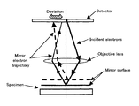
- FIG. 1 is a diagram illustrating a scanning electron microscope for performing a potential measurement method by use of mirror electrons
- FIG. 2 is a diagram illustrating a trajectory of the mirror electrons
- FIG. 3 is a diagram illustrating a method of calculating the potential of the specimen based on the trajectory of the mirror electrons
- FIG. 4 is a diagram illustrating a method of calculating, based on the trajectory of the mirror electrons, deviation of an axis of an electron beam from an objective lens;
- FIG. 5 is a schematic flow to calculate, based on the trajectory of the mirror electrons, deviation of the axis of the electron beam from the objective lens;
- FIG. 6 is a schematic flow to calculate, based on luminance of the mirror electrons, deviation of a position of a field emission electrode from an aperture;
- FIG. 7 is a schematic flow to calculate, based on the trajectory of the mirror electrons, deviation of a magnification
- FIG. 8 is a diagram illustrating a method of calculating, based on an image of the mirror electrons, deviation of a position of a structure within the apparatus
- FIG. 9 is a schematic configuration diagram of a scanning electron microscope
- FIG. 10 is a diagram illustrating a relationship among a characteristic quantity extracted from a detection result of the mirror electrons, the potential of the specimen, and the height of the specimen;
- FIG. 11 is a diagram showing a relationship between the potential and the height of the specimen when the characteristic quantity extracted from the detection result of the mirror electrons takes a specific value.
- FIG. 12 is a diagram illustrating a method of deriving the potential and the height of the specimen from the multiple characteristic quantities
- FIG. 13 is a diagram illustrating a seventh embodiment and a tenth embodiment
- FIG. 14 is a diagram illustrating an eighth embodiment
- FIG. 15 is a diagram illustrating a ninth embodiment
- FIG. 16 is a diagram illustrating a specimen information computing device
- FIG. 17 is a diagram illustrating an optical condition control device
- FIG. 18 is a diagram illustrating a twelfth embodiment.
- a measurement principle In a scanning electron microscope including: a lens including an electrode and a magnetic field, and focusing an electron beam by accelerating and decelerating the electron beam; an alignment deflector that performs axial correction; an objective lens; an aperture; and a stage that holds a specimen and applies a potential to the specimen, acceleration energy of electrons is defined as Ee, the potential applied to the specimen is defined as Vr, and
- this state is referred to as a mirror state
- the reflected electrons are referred to as a mirror electrons
- a virtual reflection plane is referred to as a mirror surface
- the reflected mirror electrons travel within the lens system in a reverse direction.
- the detector can detects arrival positions (Xm, Ym, Zm) of the mirror electrons.
- Xm, Ym, Zm arrival positions
- a charge-up voltage of the specimen can be determined from this amount of deviation. For example, by maintaining multiple data groups of Xm when changing Vr, a correlation function in which an abscissa shows Vr and an ordinate shows Xm can be created as shown in FIG. 3 . If the specimen is charged up at this time, the position of the mirror surface varies corresponding to the charge-up amount. Accordingly, even when Vr is set to Vr 1 , the arrival position of the mirror electrons deviates from Xm 1 to Xm 2 or the like. A value of Vr estimated from Xm 2 and the correlation function is Vr 2 . Since Vr 2 reflects the position of the mirror surface, Vr 2 shows the potential of the charged specimen surface. Namely, the charge-up amount ⁇ can be calculated from Vr 2 ⁇ Vr 1 .
- Ym, Zm and the like can also be used in place of Xm, for the correlation function.
- each of setting parameters (alignment deflector setting value, condensing lens setting value, deflecting coil setting value, and the like) is defined as a variable in place of Vr, and change in conditions (position deviation of apparatus configuration components, electrode and magnetic field lens, axial correction amount, magnification, and the like) of the apparatus is calculated using a correlation function acquired under reference conditions. For example, deviation of the axis of the beam from the objective lens can be calculated in the following manner.
- the setting value of the alignment deflector is defined as Ia.
- the arrival position (Xm, Ym, Zm) of the mirror electron is acquired under each of different optical conditions of an optical element (for example, voltage Vr applied to the specimen, current I obj supplied to the objective lens (voltage Vobj when the objective lens is an electrostatic lens), and the like). Then, a correlation curve between the arrival positions and the optical conditions is calculated.
- the above-mentioned Ia is varied in order to calculate the above-mentioned correlation function.
- the correlation function is calculated for each of the different las. In this state, when a current value of the alignment deflector is set to a predetermined value of Ia 1 at the time of diagnosis, the detected position of the mirror electron in a state of having no axis deviation is Xm 1 because the position agrees with the correlation function under the reference conditions.
- the detected position of the mirror electron is, for example, Xm 2 , and this position agrees with a different correlation function.
- the deviation amount of the axis at the time of diagnosis can be estimated using the amount of axis deviation corresponding to the agreed correlation function.
- the deviation amount of the axis can be estimated, for example, with the interpolation between two correlation functions which are adjacent to the detected position.
- Ia can be easily corrected using the estimated deviation amount of the beam axis.
- Vb, Io, or the like can be also used in place of Ia.
- the present method is also applicable to determination of a deviation direction of the beam axis as well as the deviation amount of the beam axis.
- FIG. 1 shows a method for diagnosing an apparatus by use of the mirror electrons, and an example of an electron microscope on which the apparatus is mounted.
- a primary electron beam 1 is extracted by applying an extraction voltage between a field emission electrode 11 and an extraction electrode 12 .
- the extracted primary electron beam 1 is accelerated by an acceleration voltage that an acceleration voltage control system 44 applies to an accelerating electrode 13 .
- the primary electron beam 1 is subjected to scanning deflection by a condensing lens 14 , an upper deflector 21 , and a lower deflector 22 . Deflection intensity of the upper deflector 21 and that of the lower deflector 22 are adjusted so that two-dimensional scanning on a specimen 23 may be performed with a lens center of an objective lens 17 serving as a fulcrum.
- the deflected primary electron beam 1 is accelerated by an acceleration cylinder 18 provided in a path of the objective lens 17 .
- the accelerated primary electron beam 1 is focused by lens action of the objective lens 17 .
- a stage voltage control system 48 applies a potential Vr to the specimen (or specimen stage (also, referred to as a specimen stand) 24 ), the potential Vr being sufficiently larger than acceleration energy Ee of the electrons.
- a storage unit 45 is a storage unit that records this information on (Xm, Ym, Zm).
- a computing element 40 calculates an amount of ‘deviation’ from the information on (Xm, Ym, Zm) on several conditions recorded in the storage unit 45 , and thus calculates an amount of changes in apparatus conditions on the basis of this amount of ‘deviation.’
- This information is sent to an analyzer 41 , so that the analyzer 41 controls the apparatus conditions therein and sets signals of parameters of a control system.
- the control system includes, for example, an alignment deflector control system 42 , an objective lens control system 43 , a deflector control system 46 , and the like, which control the apparatus conditions.
- a guide 20 is disposed and installed so as to surround a trajectory of the primary electron beam 1 .
- FIG. 5 is a schematic flow that shows an example of a method for calculating deviation of the beam from the objective lens center at the time of diagnosis based on deviation of the mirror electron trajectory.
- a setting value of an alignment deflector 25 is defined as Ia, and the detected position of the mirror electron is defined as (Xm, Ym, Zm).
- the apparatus is adjusted to the reference conditions, and is set to a mirror state.
- the setting value of the alignment deflector 25 at this time is defined as Ia 1 .
- Ia is changed, data on Xm (data on Ym or Zm may be used) is acquired, and the correlation curve between Ia and Xm is recorded in the storage unit 45 .
- the detected position of the mirror electrons is compared with the correlation function on the reference conditions stored in the storage unit 45 . Then, it is determined that when the detected position is on the correlation curve, the beam is not deviated at the time of diagnosis, and when the detected position is not on the correlation curve, the beam is deviated.
- deviation of the beam from the reference conditions is determined by acquiring the correlation curve at the time of diagnosis and comparing that with the correlation curve on the reference conditions.
- the deviation amount of the beam axis with which the correlation function at the time of diagnosis agrees is calculated in comparison with the stored correlation functions.
- the beam is emitted with the same energy, and the number Bm 2 of the detected mirror electrons at this time is calculated from the detector.
- the correlation curve between Ic and Bm can be calculated from this data.
- the correlation curve between Ic and Bin is acquired on the reference conditions in which the position of the field emission electrode having its Xt adjusted does not deviate. If position deviation is generated in the field emission electrode, the number of the electrons passing through the aperture changes. Consequently, the correlation curve between Ic and Bm changes. Therefore, position deviation of the electrolytic emission electrode can be determined from this change in correlation curve.
- a mirror electron detected position (Xin, Ym, Zin), and the like can be also used for obtaining the correlation curve.
- FIG. 6 is a schematic flowchart showing a third embodiment, which is an example of a method for diagnosing position deviation of an electron source.
- a setting value of the condensing lens is defined as Ic
- the number of the mirror electrons detected per unit time is defined as Bm.
- the apparatus is adjusted to the reference conditions, and is set to the mirror state.
- the correlation function between Ic and Bm can be acquired from data of Bm.
- the correlation curve between Ia and Bm is stored in the storage unit 45 .
- the mirror state is set at the time of diagnosis of the apparatus conditions.
- the correlation function between Ia and Bm is acquired in the same manner as in the case of the reference conditions.
- the correlation function with the reference conditions is compared with the correlation function at the time of diagnosis. If both the correlation functions agrees with each other, it is determined that there is no position deviation between the field emission electrode and the electrode, and when both do not agree, it is determined that position deviation has occurred. With the adjustment of Xt so that both the correlation functions may agree with each other in 607 , it is possible to reproduce the state where there is no position deviation.
- FIG. 7 is a flowchart showing a fourth embodiment, which is an example of a method for diagnosing change in magnification by use of the mirror electrons.
- the potential applied to the specimen is set to a value sufficiently larger than the acceleration energy Ee of the electrons
- a deflection intensity ratio of the upper deflector 21 and the lower deflector 22 is adjusted to the reference conditions, and the detected position of the mirror electrons when a setting value of a deflection amount is Id is defined as (Xm, Ym, Zm).
- the correlation function of Id and Xm (or Ym, Zm) on the reference conditions is acquired.
- Multiple correlation functions each having Id changed are acquired in 703 , and are stored in the storage unit 45 in 704 .
- the mirror state is set at the time of diagnosis of the apparatus conditions, and the detected position of the mirror electron is acquired in 706 .
- determination is made that there is no change in magnification when the acquired Xm (or Ym, Zm) agrees on the correlation function, and that there is a change in magnification when the acquired Xm (or Yin, Zm) does not agree on the correlation function.
- the deflection amount that agrees on the correlation function is calculated, and in 709 , the calculated deflection amount is fed back to the deflector control system 46 . Thereby, change in magnification is corrected.
- a method for calculating change in intensity of an objective lens at the time of diagnosis which is a fifth embodiment, can be brought into practice by replacing the variable Id of the correlation function with a setting value Io of the objective lens in FIG. 7 .
- the potential applied to the specimen is set to be sufficiently larger than the acceleration energy Ee of the electrons. Then, the primary electron beam 1 extracted by applying the extraction voltage 13 between the field emission electrode 11 and the extraction electrode 12 is accelerated in the condensing lens 14 , and passes through the aperture 15 . Then, the primary electron beam 1 is reflected above the specimen to become the mirror electron 3 , and returns to the detector 29 .
- the detectors are disposed as a detector L and a detector U as shown in FIG. 8A , an image reflected from shapes of the structures can be acquired.
- the shape of the structure A, the shape of the structure B, and a positional relation therebetween can be calculated, as shown in FIG. 8B .
- the shape of the structure B, the shape of the structure C, and the positional relation therebetween can be calculated, as shown in FIG. 8C .
- the mirror electron has an energy width smaller than that of the secondary electron and can be formed into a fine flux. Therefore, use of the mirror electron enables clearer determination of the structure.
- the mirror electron allows the apparatus diagnosis within a column, with the mirror electron not being in contact with the specimen. Accordingly, it is possible to reduce correction of apparatus condition changes over time and the machine difference between the apparatuses by calculating an appropriate adjustment value from the diagnosis result.
- the mirror electron is obtained in a state where the voltage is applied to the specimen being irradiated with a charged particle beam, in such a way that the charged particle beam fails to reach the specimen (hereinafter, this state may be referred to as the mirror state).
- this state may be referred to as the mirror state.
- the description below will be given, as an example, of a scanning electron microscope, which is an example of a charged particle beam apparatus, the present embodiment is also applicable, for example, to a focused ion beam apparatus which is other aspect of the charged particle beam apparatus.
- a positive voltage is applied to the specimen in order to form the above-mentioned mirror state.
- the detected charged particles are also cations.
- optical parameters are respectively set to an arbitrary value.
- a beam arrival position A H (X H , Y H , Z D ) (arriving point of an H trajectory on the detector) depending on a beam divergence angle on an object surface
- a beam arrival position A G (X G , Y G , Z D ) (arriving point of a G trajectory on the detector) depending on a beam position on the object surface, or both of A H and A G .
- a method for deriving the arrival position of the mirror electron will be shown below.
- Any electron detector can be selected as a detector for mirror electron, from among a detector that directly detects the mirror electron, such as MCP, a detector that causes the mirror electron to collide with a reflector or the like and detects the discharged secondary electrons, and other electron detectors.
- a detector that directly detects the mirror electron such as MCP
- a detector that causes the mirror electron to collide with a reflector or the like and detects the discharged secondary electrons and other electron detectors.
- the arrival position of the mirror electron may be determined using elements obtained by adhering a fluorescent screen to a light sensing portion of a CCD (Charge Coupled Device).
- CCD Charge Coupled Device
- the mirror electron is influenced by a path of the beam, or the structure.
- a position of an incident beam may be scanned.
- the characteristic quantity Fm can be measured by measuring a dimension of the shape of the structure transferred into the image, and sags of an edge.
- Relationships (F 1 (Vs, Zs), F 2 (Vs, Zs), . . . ) among the characteristic quantity, the potential of the specimen, and the height of the specimen under multiple optical conditions (optical condition 1 , optical condition 2 , . . . ) are stored in advance as functions or as values calculated by simulation or actual measurement, and are referred to at the time of measurement. Then, the potential and the height of the specimen can be derived from the characteristic quantities (Fm 1 , Fm 2 . . . ) acquired under the multiple optical conditions.
- optical condition 1 , optical condition 2 other than the potential Vs and the height Zs of the specimen are set, and the characteristic quantities (Fm 1 , Fm 2 ) are acquired.
- the relationship among the acquired characteristic quantity Fm, the potential Vs of the specimen, and the height Zs of the specimen is shown in FIG. 10 .
- the characteristic quantity Fm varies depending on the potential Vs and the height Zs of the specimen.
- the optical condition 1 is set and the acquired characteristic quantity is Fm 1 .
- the characteristic quantity is Fm 1 (dotted line in the drawing)
- the derived potential varies depending on the height of the specimen.
- the measured potential is VA (VB, VC).
- a relationship between the height and the potential of the specimen at this time (on the dotted line) is shown in FIG. 11 .
- the height Zs and the potential Vs of the specimen depend on each other. Therefore, when one of Zs and Vs is found, the other can be also found. Furthermore, when another optical condition (optical condition 2 ) is set and the characteristic quantity is thus acquired, both of the height Zs and the potential Vs of the specimen can be measured.
- FIG. 12 shows an explanatory view of a method of measurement.
- a solid line shows the relationship between the height Zs and the potential Vs of the specimen when the characteristic quantity acquired under the optical condition 1 (optical condition 2 ) is F 1 (F 2 ). Two curves intersect at this time. When calculating this point of intersection, the potential and the height of the specimen can be derived.
- the method for calculating an individual curve that shows the relationship between the potential Vs and the height Zs of the specimen for each optical condition, and calculating the potential and the height of the specimen from the calculated curve is shown.
- F 1 (Vs, Zs) and F 2 (Vs, Zs) may be represented by a certain function and the height Zs and the potential Vs of the specimen may be thus calculated by directly solving an equation.
- the characteristic quantity Fm may be created into a table using the height Zs and the potential Vs of the specimen, and the height Zs and the potential Vs of the specimen may be calculated by interpolation or fitting by use of points that exist adjacent to the acquired characteristic quantity Fm.
- a setting width of the optical conditions in the mirror mode can be expanded by installing structures for determining the characteristic quantity above and under the deflector.
- a method for calculating the height Zs and the potential of the specimen using a dimension of a shadow (projection image) of a first structure and a dimension of a shadow of a second structure will be shown here, the method can be also applied to other characteristic quantity.
- an on-screen length L 1 of the shadow of the first structure is determined by the magnification M obj of the objective lens, and can be represented by the following formula:
- X DEF , Y DEF deflection amount of the deflector and the inverse of the length L 1 of the shadow of the first structure is proportional to the magnification M obj that varies depending on the potential and the height of the specimen, and other optical parameters.
- a length L 2 of a shadow of the second structure varies depending on the magnification of the objective lens and the deflection amount of the deflector, as shown in the following formula:
- the potential and the height of the specimen are derived from the characteristic quantity obtained from the mirror electrons, and appropriate values suitable for observation conditions are inputted into the optical parameters, such as a holder potential Vr, an exciting current I obj of the objective lens, energy E of a primary beam, and an observing magnification.
- the optical parameters such as a holder potential Vr, an exciting current I obj of the objective lens, energy E of a primary beam, and an observing magnification.
- optical mode for observation an optical mode for observation and an optical condition (mirror mode) of the mirror mode in which the potential of the specimen is set in a way that the primary electron beam cannot reach the specimen.
- the optical condition is set to the mirror mode.
- the potential and the height of the specimen are measured, and the optical parameters in the optical mode for SEM image observation, such as the amount I obj of excitation of an objective lens 912 and the potential Vr of the specimen holder, are set from the measured result.
- FIG. 9 shows an apparatus configuration of the SEM.
- the potential of a specimen holder 905 is set to a value which prevents the primary electron beam from reaching a specimen 904 , and the optical condition is set to the mirror mode.
- arrival energy of the electron beam to the specimen is 2000 eV
- the specimen holder 905 may be referred to as a specimen stand
- the electron beam fails to reach the specimen, and is reflected by a potential barrier right in front of the specimen.
- Such a state is referred to as a mirror state, and to provide the mirror state by an adjustment of the optical conditions of the electron microscope (an acceleration voltage, the voltage applied to the specimen, and the like) is referred to as a mirror mode.
- a primary electron beam 902 is extracted from a field emission electrode 901 .
- the extracted primary electron beam 902 is accelerated by an accelerating electrode not shown.
- a voltage Vacc is applied to the accelerating electrode.
- the primary electron beam 902 is focused by a condensing lens 911 and subjected to scanning deflection by an upper deflector 906 and a lower deflector 907 .
- the deflected primary electron beam 902 is further accelerated by a boosting electrode 908 provided in a path of the objective lens 912 .
- the accelerated primary electron beam is decelerated under the influence of an electric field formed due to a potential difference between an electric field control electrode 923 and the specimen 904 , and the resultant primary electron beam is reflected right above the specimen.
- the reflected primary electron beam 903 travels backward within a mirror body.
- the primary electron beam that has traveled backward is accelerated by the boosting electrode 908 , and passes through a first structure 913 and rushes into the lower detector 921 .
- the lower detector 921 is turned OFF, the primary electron beam continues travelling backward, is subjected to deflection action by the deflector, passes through a second structure, and is detected by the upper detector 922 .
- the detected signal is inputted into a specimen information computing device 9120 , and the potential Vs and the height Zs of the specimen are derived. Then, the calculated potential Vs and height Zs of the specimen are inputted into an optical condition control device 9110 .
- a voltage and exciting current appropriate for an exiting coil and an electrode such as the electric field control electrode, the boosting electrode, an electrode which determines optical properties of the objective lens, the condensing lens, the upper deflector, the lower deflector and the like, are set in a way that focusing is made above the observed specimen based on the inputted potential and height of the specimen and the observation conditions. Thereby, an SEM image is acquired.
- the mirror electron is detected by the upper detector and the height and the potential of the specimen are calculated in the specimen information computing device 9120 .
- detection of the mirror electrons by the lower detector 921 is advantageous in that the mirror electron is not influenced by the upper deflector 906 and the lower deflector 907 at the time of a return trip.
- the present embodiment can be applied to cases where the first detector detects the characteristic quantity, where only the second detector detects the characteristic quantity, where the characteristic quantity detected by the first and second detectors are used, and the like.
- a seventh embodiment will be described using a flowchart in FIG. 13 .
- description will be given of an electron microscope having a reference data recording unit 9122 that records a function Fm (Zs, Vs) showing a relationship among the height of the specimen, and the potential of the specimen, and the characteristic quantity extracted from the detection result of the mirror electrons, or that records a table of the characteristic quantity (see FIG. 16 ).
- Step 100 the optical condition is set to the mirror mode.
- Step 110 the mirror electron is detected, and the detection result is inputted into the specimen information computing device 9120 .
- the characteristic quantity is extracted by a characteristic quantity extracting part 9121 from the inputted detection result of the mirror electrons.
- Step 130 a specimen potential and height calculation part 9123 derives the height and the potential of the specimen from the extracted characteristic quantity and the table of the characteristic quantity or the function Fm (Zs, Vs) showing the relationship among the characteristic quantity, the height of the specimen, and the potential of the specimen, the function or the table being recorded in advance for each optical condition of the mirror mode in the reference data recording unit 9122 .
- Step 140 the derived height Zs and potential Vs of the specimen, and a desired observation condition are inputted into an optical condition calculation part 9111 illustrated in FIG. 17 . Based on the inputted parameters, calculation is made on the optical parameters (potential of each electrode, amount of excitation of each exiting coil, deflection amount of the deflector, observation magnification, and the like) which cause the electron beam to focus above the specimen. The calculated optical parameters are inputted into the optical condition setting part 9112 , and the potential and exciting current for each electrode and the exciting coil are thus set respectively.
- the above-mentioned characteristic quantity denotes the detected position of the electron on the detector, the dimension of the structure on the image, the position of the structure, sags of the edge, the amount of rotation, luminance, and the like. All of them can be detected using existing techniques.
- the dimension of the structure is detected based on the magnification of the electron microscope, an occupation percentage of the structure on the image, and the like; the position of the structure based on general image processing techniques for identifying the position of the structure on the image; sagging of the edge based on a sharp evaluation that is used for a focus adjustment, and the like; the amount of rotation, about degrees of rotation of the target structure on the image, based on general image processing techniques; and the luminance based on luminance histogram formation of the image.
- a method for deriving the height and the potential of the specimen using the characteristic quantity extracted from the shadow of the structure will be shown as an eighth embodiment.
- the present embodiment shows a case where the structure in a shape of 1 is installed in the position of the first structure 913 , and the mirror electron is detected by the upper detector 922 while the electron beam is scanned by the upper deflector 906 and the lower deflector 907 .
- the positional relation of the detectors or the structures may be changed.
- the image having characteristics depending on the shape of the structure is obtained from the detection result of the mirror electron.
- the dimension of the structure, sags of the edge, the amount of rotation, and the luminance thus obtained are converted into numbers as the characteristic quantity, and the height and the potential of the specimen are derived.
- an electron microscope will be shown, in which a structure installed on mirror electron trajectory is installed both above and below a deflector, and based on a ratio or difference of the characteristic quantities extracted from the shadows of the structures installed above and below the deflector, the potential and the height of the specimen are measured.
- a first structure 913 in a shape of 1 is installed below the deflector, and the second structure 914 in a shape of “2” is installed above the deflector.
- the electron beam is scanned by the upper deflector 906 and the lower deflector 907 , the mirror electron is detected by the upper detector 922 . Thereby, the image as shown in FIG. 15 can be acquired.
- an electron microscope that measures the height and the potential of the specimen from the characteristic quantities acquired under the optical condition in multiple mirror modes will be shown. If the number of the characteristic quantities has not reached yet the desired number at the time of checking the number of the characteristic quantities at Step 160 in the flowchart shown in FIG. 13 , the electron microscope sets the optical condition to a new mirror mode, and extracts a new characteristic quantity in Step 170 .
- two or more characteristic quantities for example, sags of the edge and the dimension of the structure, a beam diameter on a detecting surface and a deflecting width, or the like, may be extracted from the detection result of the mirror electron under a single optical condition.
- an electron microscope that holds a calibration specimen on the specimen holder will be shown.
- This calibration specimen is used to ensure an absolute value of the potential or focus conditions. It is desirable that the calibration specimen should be a conductor, located approximately at the same height as the observed specimen, and grounded to the specimen holder so as to have the same potential as that of the specimen holder.
- a reference data is acquired in advance from the calibration specimen, an error of measurement generated by changes of the optical conditions over time can be reduced.
- an electron microscope that holds, on a wafer holder, a calibration specimen for adjusting changes of the optical condition over time and updates a measured value or function stored in the reference data recording unit 9122 will be shown.
- FIG. 18 shows a flowchart of the twelfth embodiment. Determination is made as to whether reference data is updated in Step 200 .
- the reference data may be periodically updated, or may be automatically updated when focus deviation at the time of observation becomes remarkable.
- Step 210 the measurement target is changed to a calibration specimen for reference data.
- Step 220 the mirror mode in which the reference data is updated is set.
- Step 230 and Step 240 the mirror electron is detected and the characteristic quantity is extracted.
- the height of the calibration specimen is measured from a Z sensor, an exciting current of normal SEM observation, and multiple characteristic quantities extracted in the mirror mode.
- Step 260 the relationship among the height of the specimen, the potential of the specimen, and the characteristic quantity obtained from Step 210 to Step 250 is stored in the reference data recording unit 9122 .
- the reference data is acquired under each of the optical conditions of multiple heights and in multiple mirror modes. Thereby, even when changes over time are generated in the optical condition in the mirror mode, the height and the potential of the specimen can be accurately measured. Additionally, before SEM image observation, the optical conditions such as focus, magnification, and observation position, can be adjusted without irradiating the specimen with the electron beam.
Abstract
Description
where
Accordingly, when a ratio (L1/L2) of the length L1 of the shadow of the first structure to the length L2 of the shadow of the second structure is extracted as the characteristic quantity, a magnitude of the characteristic quantity can be varied to a desired deflection amount, independent of the deflection amount of the deflector. For this reason, the setting width of the optical conditions in the mirror mode can be expanded.
Claims (20)
Priority Applications (1)
| Application Number | Priority Date | Filing Date | Title |
|---|---|---|---|
| US13/300,117 US8487253B2 (en) | 2008-03-05 | 2011-11-18 | Scanning electron microscope |
Applications Claiming Priority (4)
| Application Number | Priority Date | Filing Date | Title |
|---|---|---|---|
| JP2008-054229 | 2008-03-05 | ||
| JP2008054227A JP5216371B2 (en) | 2008-03-05 | 2008-03-05 | Scanning electron microscope |
| JP2008-054227 | 2008-03-05 | ||
| JP2008054229A JP5210666B2 (en) | 2008-03-05 | 2008-03-05 | Scanning electron microscope |
Related Child Applications (1)
| Application Number | Title | Priority Date | Filing Date |
|---|---|---|---|
| US13/300,117 Continuation US8487253B2 (en) | 2008-03-05 | 2011-11-18 | Scanning electron microscope |
Publications (2)
| Publication Number | Publication Date |
|---|---|
| US20090224170A1 US20090224170A1 (en) | 2009-09-10 |
| US8080790B2 true US8080790B2 (en) | 2011-12-20 |
Family
ID=41052649
Family Applications (2)
| Application Number | Title | Priority Date | Filing Date |
|---|---|---|---|
| US12/392,563 Expired - Fee Related US8080790B2 (en) | 2008-03-05 | 2009-02-25 | Scanning electron microscope |
| US13/300,117 Active US8487253B2 (en) | 2008-03-05 | 2011-11-18 | Scanning electron microscope |
Family Applications After (1)
| Application Number | Title | Priority Date | Filing Date |
|---|---|---|---|
| US13/300,117 Active US8487253B2 (en) | 2008-03-05 | 2011-11-18 | Scanning electron microscope |
Country Status (1)
| Country | Link |
|---|---|
| US (2) | US8080790B2 (en) |
Cited By (4)
| Publication number | Priority date | Publication date | Assignee | Title |
|---|---|---|---|---|
| US20090189062A1 (en) * | 2008-01-24 | 2009-07-30 | Jeol Ltd. | Method of Calibrating Beam Position in Charged-Particle Beam System |
| US20120061566A1 (en) * | 2008-03-05 | 2012-03-15 | Hitachi High-Technologies Corporation | Scanning electron microscope |
| US20120217392A1 (en) * | 2011-02-28 | 2012-08-30 | Tsutomu Murakawa | Pattern-height measuring apparatus and pattern-height measuring method |
| WO2022033717A1 (en) * | 2020-08-11 | 2022-02-17 | Carl Zeiss Multisem Gmbh | Multiple particle beam system with a mirror mode of operation, method for operating a multiple particle beam system with a mirror mode of operation and associated computer program product |
Families Citing this family (6)
| Publication number | Priority date | Publication date | Assignee | Title |
|---|---|---|---|---|
| JP5222994B2 (en) | 2009-02-20 | 2013-06-26 | 株式会社日立ハイテクノロジーズ | Sample observation method and scanning electron microscope |
| CZ304659B6 (en) * | 2013-04-19 | 2014-08-20 | Delong Instruments A.S. | Detection method of signal electrons in electron microscope and apparatus for making the same |
| JP6383228B2 (en) * | 2014-09-19 | 2018-08-29 | 株式会社ニューフレアテクノロジー | Beam position measuring method for multi charged particle beam and multi charged particle beam drawing apparatus |
| JP6433515B2 (en) * | 2015-02-09 | 2018-12-05 | 株式会社日立製作所 | Mirror ion microscope and ion beam control method |
| JP2018174016A (en) * | 2015-07-29 | 2018-11-08 | 株式会社日立ハイテクノロジーズ | Charged particle beam device |
| US10790114B2 (en) | 2017-06-29 | 2020-09-29 | Kla-Tencor Corporation | Scanning electron microscope objective lens calibration using X-Y voltages iteratively determined from images obtained using said voltages |
Citations (12)
| Publication number | Priority date | Publication date | Assignee | Title |
|---|---|---|---|---|
| JPH11149895A (en) | 1997-08-11 | 1999-06-02 | Hitachi Ltd | Electron beam inspection or measuring apparatus and its method, height detection apparatus, and electron beam drawing apparatus |
| US6107637A (en) | 1997-08-11 | 2000-08-22 | Hitachi, Ltd. | Electron beam exposure or system inspection or measurement apparatus and its method and height detection apparatus |
| JP2001236915A (en) | 1999-09-03 | 2001-08-31 | Applied Materials Inc | Focusing method and system |
| US6633034B1 (en) * | 2000-05-04 | 2003-10-14 | Applied Materials, Inc. | Method and apparatus for imaging a specimen using low profile electron detector for charged particle beam imaging apparatus including electrostatic mirrors |
| US6946656B2 (en) | 2001-07-12 | 2005-09-20 | Hitachi, Ltd. | Sample electrification measurement method and charged particle beam apparatus |
| JP2005276639A (en) | 2004-03-25 | 2005-10-06 | Jeol Ltd | Position adjusting method for objective lens diaphragm of scanning type electron beam device |
| JP2005338096A (en) | 2001-07-12 | 2005-12-08 | Hitachi Ltd | Pattern measuring method and charged particle beam device |
| US20060011835A1 (en) * | 2004-07-15 | 2006-01-19 | Hisaya Murakoshi | Electron microscope and electron beam inspection system |
| US20070120065A1 (en) | 2005-11-18 | 2007-05-31 | Atsushi Takane | Charged particle beam apparatus |
| US20080191135A1 (en) * | 2007-01-30 | 2008-08-14 | Hitachi High-Technologies Corporation | Scanning Electron Microscope |
| US20090261252A1 (en) * | 2006-02-06 | 2009-10-22 | Hitachi High-Technologies Corporation. | Method and apparatus for pattern inspection |
| US20100213370A1 (en) * | 2005-02-17 | 2010-08-26 | Mamoru Nakasuji | Electron Beam Apparatus |
Family Cites Families (2)
| Publication number | Priority date | Publication date | Assignee | Title |
|---|---|---|---|---|
| US6688487B2 (en) | 2001-04-13 | 2004-02-10 | The Coca-Cola Company | Locking cup and lid with negative draft sealing surfaces |
| US8080790B2 (en) * | 2008-03-05 | 2011-12-20 | Hitachi High-Technologies Corporation | Scanning electron microscope |
-
2009
- 2009-02-25 US US12/392,563 patent/US8080790B2/en not_active Expired - Fee Related
-
2011
- 2011-11-18 US US13/300,117 patent/US8487253B2/en active Active
Patent Citations (14)
| Publication number | Priority date | Publication date | Assignee | Title |
|---|---|---|---|---|
| US6107637A (en) | 1997-08-11 | 2000-08-22 | Hitachi, Ltd. | Electron beam exposure or system inspection or measurement apparatus and its method and height detection apparatus |
| JPH11149895A (en) | 1997-08-11 | 1999-06-02 | Hitachi Ltd | Electron beam inspection or measuring apparatus and its method, height detection apparatus, and electron beam drawing apparatus |
| JP2001236915A (en) | 1999-09-03 | 2001-08-31 | Applied Materials Inc | Focusing method and system |
| US6521891B1 (en) | 1999-09-03 | 2003-02-18 | Applied Materials, Inc. | Focusing method and system |
| US6633034B1 (en) * | 2000-05-04 | 2003-10-14 | Applied Materials, Inc. | Method and apparatus for imaging a specimen using low profile electron detector for charged particle beam imaging apparatus including electrostatic mirrors |
| JP2005338096A (en) | 2001-07-12 | 2005-12-08 | Hitachi Ltd | Pattern measuring method and charged particle beam device |
| US6946656B2 (en) | 2001-07-12 | 2005-09-20 | Hitachi, Ltd. | Sample electrification measurement method and charged particle beam apparatus |
| JP2005276639A (en) | 2004-03-25 | 2005-10-06 | Jeol Ltd | Position adjusting method for objective lens diaphragm of scanning type electron beam device |
| US20060011835A1 (en) * | 2004-07-15 | 2006-01-19 | Hisaya Murakoshi | Electron microscope and electron beam inspection system |
| US20100213370A1 (en) * | 2005-02-17 | 2010-08-26 | Mamoru Nakasuji | Electron Beam Apparatus |
| US20070120065A1 (en) | 2005-11-18 | 2007-05-31 | Atsushi Takane | Charged particle beam apparatus |
| JP2007141632A (en) | 2005-11-18 | 2007-06-07 | Hitachi High-Technologies Corp | Charged particle beam device |
| US20090261252A1 (en) * | 2006-02-06 | 2009-10-22 | Hitachi High-Technologies Corporation. | Method and apparatus for pattern inspection |
| US20080191135A1 (en) * | 2007-01-30 | 2008-08-14 | Hitachi High-Technologies Corporation | Scanning Electron Microscope |
Cited By (7)
| Publication number | Priority date | Publication date | Assignee | Title |
|---|---|---|---|---|
| US20090189062A1 (en) * | 2008-01-24 | 2009-07-30 | Jeol Ltd. | Method of Calibrating Beam Position in Charged-Particle Beam System |
| US8193511B2 (en) * | 2008-01-24 | 2012-06-05 | Jeol Ltd. | Method of calibrating beam position in charged-particle beam system |
| US20120061566A1 (en) * | 2008-03-05 | 2012-03-15 | Hitachi High-Technologies Corporation | Scanning electron microscope |
| US8487253B2 (en) * | 2008-03-05 | 2013-07-16 | Hitachi High-Technologies Corporation | Scanning electron microscope |
| US20120217392A1 (en) * | 2011-02-28 | 2012-08-30 | Tsutomu Murakawa | Pattern-height measuring apparatus and pattern-height measuring method |
| US8604431B2 (en) * | 2011-02-28 | 2013-12-10 | Advantest Corp. | Pattern-height measuring apparatus and pattern-height measuring method |
| WO2022033717A1 (en) * | 2020-08-11 | 2022-02-17 | Carl Zeiss Multisem Gmbh | Multiple particle beam system with a mirror mode of operation, method for operating a multiple particle beam system with a mirror mode of operation and associated computer program product |
Also Published As
| Publication number | Publication date |
|---|---|
| US8487253B2 (en) | 2013-07-16 |
| US20090224170A1 (en) | 2009-09-10 |
| US20120061566A1 (en) | 2012-03-15 |
Similar Documents
| Publication | Publication Date | Title |
|---|---|---|
| US8080790B2 (en) | Scanning electron microscope | |
| JP3951590B2 (en) | Charged particle beam equipment | |
| US8766182B2 (en) | Method for detecting information of an electric potential on a sample and charged particle beam apparatus | |
| US7385198B2 (en) | Method and apparatus for measuring the physical properties of micro region | |
| US8993961B2 (en) | Electric charged particle beam microscope and electric charged particle beam microscopy | |
| JP5241168B2 (en) | electronic microscope | |
| JPH11108864A (en) | Method and apparatus for inspecting pattern flaw | |
| CN108604522B (en) | Charged particle beam device and method for adjusting charged particle beam device | |
| US20070187599A1 (en) | Charged particle beam apparatus, charged particle beam focusing method, microstructure measuring method, microstructure inspecting method, semiconductor device manufacturing method, and program | |
| KR20140143441A (en) | Charged particle beam device | |
| US6653631B2 (en) | Apparatus and method for defect detection using charged particle beam | |
| JP5438937B2 (en) | Charged particle beam equipment | |
| TWI818324B (en) | Charged particle beam device and control method | |
| JP5216371B2 (en) | Scanning electron microscope | |
| US6992287B2 (en) | Apparatus and method for image optimization of samples in a scanning electron microscope | |
| JP4431624B2 (en) | Charged particle beam adjustment method and charged particle beam apparatus | |
| JP5210666B2 (en) | Scanning electron microscope | |
| JP5174483B2 (en) | Charged particle beam apparatus and method for knowing charged state of sample surface | |
| JP2007205965A (en) | Height detecting device used for charged particle beam device and height detecting method |
Legal Events
| Date | Code | Title | Description |
|---|---|---|---|
| AS | Assignment |
Owner name: HITACHI HIGH-TECHNOLOGIES CORPORATION, JAPAN Free format text: ASSIGNMENT OF ASSIGNORS INTEREST;ASSIGNORS:YAMAZAKI, MINORU;IKEGAMI, AKIRA;KAZUMI, HIDEYUKI;AND OTHERS;REEL/FRAME:022682/0692;SIGNING DATES FROM 20090319 TO 20090330 Owner name: HITACHI HIGH-TECHNOLOGIES CORPORATION, JAPAN Free format text: ASSIGNMENT OF ASSIGNORS INTEREST;ASSIGNORS:YAMAZAKI, MINORU;IKEGAMI, AKIRA;KAZUMI, HIDEYUKI;AND OTHERS;SIGNING DATES FROM 20090319 TO 20090330;REEL/FRAME:022682/0692 |
|
| ZAAA | Notice of allowance and fees due |
Free format text: ORIGINAL CODE: NOA |
|
| ZAAB | Notice of allowance mailed |
Free format text: ORIGINAL CODE: MN/=. |
|
| FEPP | Fee payment procedure |
Free format text: PAYOR NUMBER ASSIGNED (ORIGINAL EVENT CODE: ASPN); ENTITY STATUS OF PATENT OWNER: LARGE ENTITY |
|
| STCF | Information on status: patent grant |
Free format text: PATENTED CASE |
|
| FPAY | Fee payment |
Year of fee payment: 4 |
|
| MAFP | Maintenance fee payment |
Free format text: PAYMENT OF MAINTENANCE FEE, 8TH YEAR, LARGE ENTITY (ORIGINAL EVENT CODE: M1552); ENTITY STATUS OF PATENT OWNER: LARGE ENTITY Year of fee payment: 8 |
|
| AS | Assignment |
Owner name: HITACHI HIGH-TECH CORPORATION, JAPAN Free format text: CHANGE OF NAME AND ADDRESS;ASSIGNOR:HITACHI HIGH-TECHNOLOGIES CORPORATION;REEL/FRAME:052259/0227 Effective date: 20200212 |
|
| FEPP | Fee payment procedure |
Free format text: MAINTENANCE FEE REMINDER MAILED (ORIGINAL EVENT CODE: REM.); ENTITY STATUS OF PATENT OWNER: LARGE ENTITY |
|
| LAPS | Lapse for failure to pay maintenance fees |
Free format text: PATENT EXPIRED FOR FAILURE TO PAY MAINTENANCE FEES (ORIGINAL EVENT CODE: EXP.); ENTITY STATUS OF PATENT OWNER: LARGE ENTITY |
|
| STCH | Information on status: patent discontinuation |
Free format text: PATENT EXPIRED DUE TO NONPAYMENT OF MAINTENANCE FEES UNDER 37 CFR 1.362 |
|
| FP | Lapsed due to failure to pay maintenance fee |
Effective date: 20231220 |