JP5196330B2 - 静電気対策素子及びその複合電子部品 - Google Patents
静電気対策素子及びその複合電子部品 Download PDFInfo
- Publication number
- JP5196330B2 JP5196330B2 JP2009248089A JP2009248089A JP5196330B2 JP 5196330 B2 JP5196330 B2 JP 5196330B2 JP 2009248089 A JP2009248089 A JP 2009248089A JP 2009248089 A JP2009248089 A JP 2009248089A JP 5196330 B2 JP5196330 B2 JP 5196330B2
- Authority
- JP
- Japan
- Prior art keywords
- electrodes
- layer
- insulating
- inorganic material
- composite
- Prior art date
- Legal status (The legal status is an assumption and is not a legal conclusion. Google has not performed a legal analysis and makes no representation as to the accuracy of the status listed.)
- Active
Links
Images

Classifications
-
- H—ELECTRICITY
- H01—ELECTRIC ELEMENTS
- H01T—SPARK GAPS; OVERVOLTAGE ARRESTERS USING SPARK GAPS; SPARKING PLUGS; CORONA DEVICES; GENERATING IONS TO BE INTRODUCED INTO NON-ENCLOSED GASES
- H01T4/00—Overvoltage arresters using spark gaps
- H01T4/08—Overvoltage arresters using spark gaps structurally associated with protected apparatus
-
- H—ELECTRICITY
- H10—SEMICONDUCTOR DEVICES; ELECTRIC SOLID-STATE DEVICES NOT OTHERWISE PROVIDED FOR
- H10D—INORGANIC ELECTRIC SEMICONDUCTOR DEVICES
- H10D89/00—Aspects of integrated devices not covered by groups H10D84/00 - H10D88/00
- H10D89/60—Integrated devices comprising arrangements for electrical or thermal protection, e.g. protection circuits against electrostatic discharge [ESD]
-
- H—ELECTRICITY
- H01—ELECTRIC ELEMENTS
- H01F—MAGNETS; INDUCTANCES; TRANSFORMERS; SELECTION OF MATERIALS FOR THEIR MAGNETIC PROPERTIES
- H01F17/00—Fixed inductances of the signal type
- H01F2017/0093—Common mode choke coil
Landscapes
- Thermistors And Varistors (AREA)
- Coils Or Transformers For Communication (AREA)
- Elimination Of Static Electricity (AREA)
Description
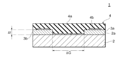
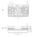
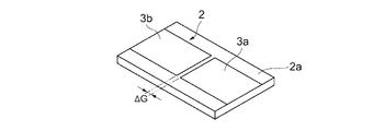
図1は、本発明による静電気対策素子の好ましい実施形態を概略的に示す模式断面図である。この静電気対策素子1は、絶縁性表面2aを有する基体2と、この絶縁性表面2a上に配設された一対の電極3a,3bと、これら電極3a,3bの間に配設された機能層4と、電極3a,3bと電気的に接続された端子電極5(図示せず)と、を備える。この静電気対策素子1において、機能層4は低電圧放電タイプの静電気保護材料として機能し、静電気などの過電圧が印加された際に、この機能層4を介して電極3a,3b間で初期放電が確保されるように設計されている。
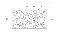
機能層4は、絶縁性無機材料4aのマトリックス中に島状の導電性無機材料4bの集合体が不連続に点在した海島構造のコンポジットから構成されている。本実施形態では、機能層4は、逐次スパッタリングを行うことにより形成されている。より具体的には、基体2の絶縁性表面2a上及び/又は電極3a,3b上に、導電性無機材料4bをスパッタリングして部分的に(不完全に)成膜した後、引き続き絶縁性無機材料4aをスパッタリングすることにより、謂わば、島状に点在した導電性無機材料4bの層とこれを覆う絶縁性無機材料4aの層との積層構造のコンポジットが形成されている。
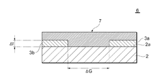
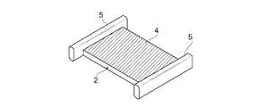
図3は、本発明による静電気対策素子の他の好ましい実施形態を概略的に示す模式断面図である。この静電気対策素子6は、機能層4に代えて機能層7を有する他は、上述した第1実施形態の静電気対策素子1と同じ構成を有する。
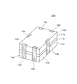
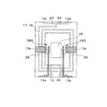
図4は、本発明による複合電子部品の好ましい実施形態の外観構成を概略的に示す斜視図である。
図9に示すように、まず、絶縁性の基体2(NiZnフェライト基板、誘電率:13、TDK株式会社製)の一方の絶縁性表面2a上に、スパッタリング法により、下地層(密着層)として厚み10nmのクロム薄膜を形成し、その後、このクロム薄膜上に、スパッタリング法により、厚み0.1μmのCu薄膜を略全面に形成することにより、クロムと銅の2層構造からなる金属薄膜を形成した。次に、形成されたCu薄膜の上面に、ロールコーターを用いてネガ型フォトレジストをベタ塗布した後、これを温度95℃及び3〜15分の条件下で乾燥させ、厚み2〜6μmのレジスト層を形成した。その後、電極間のギャップに相当する部分のみをマスクした状態で、露光処理を行ない、電極間のギャップに相当する部分以外を硬化させ、未露光部分のレジスト層を現像除去した。次いで、露出したCu薄膜(電極間のギャップに相当する部分)を、イオンミリングによりエッチングすることにより、相互に離間して対向配置された一対の帯状の電極3a,3bを形成した。このとき、電極3a,3b間のギャップ距離△Gは、1μmとした。
電極3a,3bの厚みを0.2μmに変更すること以外は、実施例1と同様に操作して、実施例2の静電気対策素子1を得た。
電極3a,3bの厚みを0.4μmに変更すること以外は、実施例1と同様に操作して、実施例3の静電気対策素子1を得た。
電極3a,3b間のギャップ距離△Gを2μmに変更すること以外は、実施例3と同様に操作して、実施例4の静電気対策素子1を得た。
電極3a,3b間のギャップ距離△Gを2.5μmに変更すること以外は、実施例1と同様に操作して、実施例5の静電気対策素子1を得た。
電極3a,3b間のギャップ距離△Gを5μmに変更し、機能層4の形成を省略すること以外は、実施例1と同様に操作して、比較例1の静電気対策素子1を得た。
電極3a,3b間のギャップ距離△Gを5μmに変更し、機能層4の形成時の導電性無機材料4bのスパッタリングを省略すること以外は、実施例1と同様に操作して、比較例2の静電気対策素子1を得た。
電極3a,3b間のギャップ距離△Gを5μmに変更すること以外は、実施例1と同様に操作して、比較例3の静電気対策素子を得た。
電極3a,3b間のギャップ距離△Gを3.5μmに変更すること以外は、実施例1と同様に操作して、比較例4の静電気対策素子を得た。
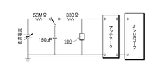
次に、上記のようにして得られた実施例1〜3並びに比較例1〜3の静電気対策素子について、図12に示す静電気試験回路を用いて、静電気放電試験を実施した。
電極3a,3bの作製時に使用する金属をCuに代えてAg、Au、Alに変更すること以外は、実施例3と同様に操作して、実施例6〜8の静電気対策素子1を得た。表2に、評価結果を示す。
Claims (6)
- 絶縁性表面を有する基体と、該絶縁性表面上において相互に離間して対向配置された電極と、少なくとも該電極間に配置された機能層とを備え、
前記機能層は、絶縁性無機材料のマトリックス中に導電性無機材料が不連続に分散したコンポジットであり、且つ、スパッタリング法によって形成されたものであり、
前記電極間のギャップ距離ΔGが、0.5〜10μm(但し、3.5μm以上の場合を除く。)であり、
前記電極の厚みΔTが、ΔG/ΔT=1〜30の関係を満たす、
静電気対策素子。 - 前記絶縁性無機材料は、Al2O3、TiO2、SiO2、ZnO、In2O3、NiO、CoO、SnO2、V2O5、CuO、MgO、ZrO2、AlN、BN及びSiCよりなる群から選択される少なくとも1種である、
請求項1に記載の静電気対策素子。 - 前記導電性無機材料は、C、Ni、Cu、Au、Ti、Cr、Ag、Pd及びPtよりなる群から選択される少なくとも1種の金属又はこれらの金属化合物である、
請求項1又は2に記載の静電気対策素子。 - 前記電極は、Cu、Au、Cr、Al、Ag、Zn、W、Mo、Ni、Co及びFeから選ばれる少なくとも一種類の金属或いはこれらの合金である、
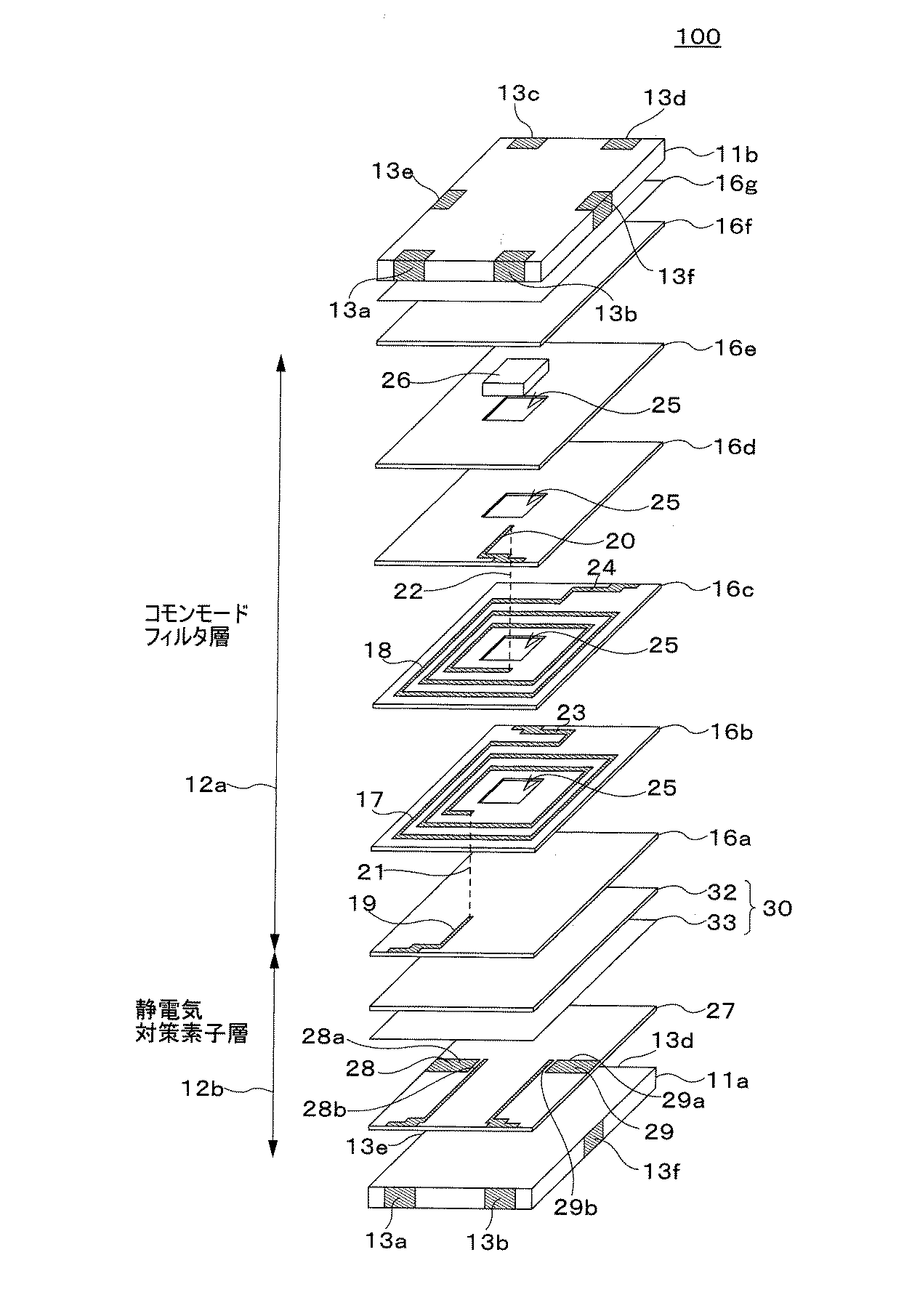
請求項1〜3のいずれか一項に記載の静電気対策素子。 - 2つの磁性基体の間にインダクタ素子と静電気対策素子とを有する複合電子部品であって、
前記インダクタ素子は、樹脂からなる絶縁層と、前記絶縁層上に形成された導体パターンとを備え、
前記静電気対策素子は、前記磁性基体上に形成された下地絶縁層と、該下地絶縁層上において相互に離間して対向配置された電極と、少なくとも該電極間に配置された機能層とを備え、
前記機能層は、絶縁性無機材料のマトリックス中に導電性無機材料が不連続に分散したコンポジットであり、且つ、スパッタリング法によって形成されたものであり、
前記電極間のギャップ距離ΔGが、0.5〜10μm(但し、3.5μm以上の場合を除く。)であり、
前記電極の厚みΔTが、ΔG/ΔT=1〜30の関係を満たす、
複合電子部品。 - 2つの磁性基体の間に設けられたコモンモードフィルタ層及び静電気対策素子層とを備え、
前記コモンモードフィルタ層は、
樹脂からなる第1及び第2の絶縁層と、
前記第1の絶縁層上に形成された第1のスパイラル導体と、
前記第2の絶縁層上に形成された第2のスパイラル導体とを備え、
前記静電気対策素子層は、
前記第1のスパイラル導体の一端に接続された第1の静電気対策素子と、
前記第2のスパイラル導体の一端に接続された第2の静電気対策素子とを備え、
前記第1及び第2のスパイラル導体は、積層方向と垂直な平面にそれぞれ形成され、互いに磁気結合するように配置され、
前記第1及び第2の静電気対策素子は、前記磁性基体上に形成された下地絶縁層と、該下地絶縁層上において相互に離間して対向配置された電極と、少なくとも該電極間に配置された機能層と備え、
前記機能層は、絶縁性無機材料のマトリックス中に導電性無機材料が不連続に分散したコンポジットであり、且つ、スパッタリング法によって形成されたものであり、
前記電極間のギャップ距離ΔGが、0.5〜10μm(但し、3.5μm以上の場合を除く。)であり、
前記電極の厚みΔTが、ΔG/ΔT=1〜30の関係を満たす、
複合電子部品。
Priority Applications (3)
| Application Number | Priority Date | Filing Date | Title |
|---|---|---|---|
| JP2009248089A JP5196330B2 (ja) | 2008-12-18 | 2009-10-28 | 静電気対策素子及びその複合電子部品 |
| US12/654,210 US8199451B2 (en) | 2008-12-18 | 2009-12-14 | ESD protection device and composite electronic component of the same |
| KR1020090124857A KR20100070997A (ko) | 2008-12-18 | 2009-12-15 | 정전기 대책 소자 및 그 복합 전자 부품 |
Applications Claiming Priority (3)
| Application Number | Priority Date | Filing Date | Title |
|---|---|---|---|
| JP2008322433 | 2008-12-18 | ||
| JP2008322433 | 2008-12-18 | ||
| JP2009248089A JP5196330B2 (ja) | 2008-12-18 | 2009-10-28 | 静電気対策素子及びその複合電子部品 |
Publications (2)
| Publication Number | Publication Date |
|---|---|
| JP2010165665A JP2010165665A (ja) | 2010-07-29 |
| JP5196330B2 true JP5196330B2 (ja) | 2013-05-15 |
Family
ID=42265713
Family Applications (1)
| Application Number | Title | Priority Date | Filing Date |
|---|---|---|---|
| JP2009248089A Active JP5196330B2 (ja) | 2008-12-18 | 2009-10-28 | 静電気対策素子及びその複合電子部品 |
Country Status (3)
| Country | Link |
|---|---|
| US (1) | US8199451B2 (ja) |
| JP (1) | JP5196330B2 (ja) |
| KR (1) | KR20100070997A (ja) |
Families Citing this family (17)
| Publication number | Priority date | Publication date | Assignee | Title |
|---|---|---|---|---|
| US8422190B2 (en) * | 2008-09-30 | 2013-04-16 | Tdk Corporation | Composite electronic device, manufacturing method thereof, and connection structure of composite electronic device |
| JP5196330B2 (ja) * | 2008-12-18 | 2013-05-15 | Tdk株式会社 | 静電気対策素子及びその複合電子部品 |
| JP4835699B2 (ja) * | 2009-01-22 | 2011-12-14 | Tdk株式会社 | 高速デジタル伝送回路 |
| JP4749482B2 (ja) * | 2009-07-08 | 2011-08-17 | Tdk株式会社 | 複合電子部品 |
| JP2012074228A (ja) * | 2010-09-28 | 2012-04-12 | Tdk Corp | 静電気対策素子 |
| JP2013175443A (ja) * | 2012-01-27 | 2013-09-05 | Tdk Corp | 静電気対策素子 |
| KR101792269B1 (ko) * | 2012-04-05 | 2017-11-01 | 삼성전기주식회사 | 전자부품 및 전자부품 제조방법 |
| KR101771726B1 (ko) * | 2012-06-18 | 2017-08-25 | 삼성전기주식회사 | 정전기 방지 소자 및 이를 포함하는 복합 전자 부품 |
| JP5784688B2 (ja) | 2012-12-10 | 2015-09-24 | サムソン エレクトロ−メカニックス カンパニーリミテッド. | 静電気放電構造及び静電気放電構造の製造方法 |
| KR101719841B1 (ko) * | 2012-12-10 | 2017-03-24 | 삼성전기주식회사 | 공통모드필터 |
| KR101912270B1 (ko) * | 2013-07-26 | 2018-10-29 | 삼성전기 주식회사 | 공통모드필터 |
| US9293913B2 (en) * | 2013-08-01 | 2016-03-22 | Tdk Corporation | ESD protection component and method for manufacturing ESD protection component |
| KR101983159B1 (ko) * | 2013-11-28 | 2019-05-28 | 삼성전기주식회사 | 코일 부품 및 이의 제조 방법 |
| KR20160024262A (ko) * | 2014-08-25 | 2016-03-04 | 삼성전기주식회사 | 공통 모드 필터 및 그 제조 방법 |
| WO2017038238A1 (ja) * | 2015-09-01 | 2017-03-09 | 株式会社村田製作所 | Esd保護素子 |
| CN105810677B (zh) | 2016-05-16 | 2019-01-29 | 京东方科技集团股份有限公司 | 静电释放组件、阵列基板及其制备方法、显示面板 |
| CN113363098A (zh) * | 2021-03-30 | 2021-09-07 | 中国石油大学(华东) | 一种井下作业的自熄弧放电开关结构 |
Family Cites Families (22)
| Publication number | Priority date | Publication date | Assignee | Title |
|---|---|---|---|---|
| US2924734A (en) * | 1955-06-09 | 1960-02-09 | Siemens Ag | Spark gap device |
| US3704388A (en) * | 1970-07-06 | 1972-11-28 | Asea Ab | Spark gap for surge diverters |
| GB1358043A (en) * | 1970-07-21 | 1974-06-26 | Atomic Energy Authority Uk | Electrical spark gap switch apparatus |
| DE2528174C3 (de) * | 1975-06-24 | 1978-06-22 | Hans Dipl.-Phys. Dr. 7000 Stuttgart Salzmann | Laser mit Wanderwellenanregung |
| US6191928B1 (en) | 1994-05-27 | 2001-02-20 | Littelfuse, Inc. | Surface-mountable device for protection against electrostatic damage to electronic components |
| JP3455011B2 (ja) * | 1996-05-07 | 2003-10-06 | アルプス電気株式会社 | サージアブソーバおよびその製造方法 |
| JP3817995B2 (ja) * | 1999-11-30 | 2006-09-06 | 三菱マテリアル株式会社 | サージ吸収素子及びその製造方法 |
| DE20020771U1 (de) * | 2000-02-22 | 2001-02-15 | Dehn & Soehne | Druckfest gekapselte Funkenstreckenanordnung zum Ableiten von schädlichen Störgrößen durch Überspannung |
| DE60136989D1 (de) * | 2000-02-29 | 2009-01-29 | Ngk Spark Plug Co | Zündkerze |
| JP2002015831A (ja) | 2000-06-30 | 2002-01-18 | Mitsubishi Materials Corp | チップ型サージアブソーバ及びその製造方法 |
| JP3900104B2 (ja) * | 2003-04-10 | 2007-04-04 | 松下電器産業株式会社 | 静電気対策部品 |
| JP4725343B2 (ja) * | 2006-02-07 | 2011-07-13 | パナソニック株式会社 | 複合電子部品およびその製造方法 |
| JP2007242404A (ja) | 2006-03-08 | 2007-09-20 | Mitsubishi Materials Corp | サージアブソーバ |
| JP2007265713A (ja) | 2006-03-28 | 2007-10-11 | Matsushita Electric Ind Co Ltd | 静電気保護材料ペーストおよびそれを用いた静電気対策部品 |
| KR100813195B1 (ko) | 2006-04-20 | 2008-03-13 | 주식회사 이노칩테크놀로지 | 정전기 보호 소자 |
| US7733620B2 (en) * | 2006-07-19 | 2010-06-08 | Ta-I Technology Co., Ltd | Chip scale gas discharge protective device and fabrication method of the same |
| TW200816232A (en) * | 2006-09-28 | 2008-04-01 | Inpaq Technology Co Ltd | Material of an over voltage protection device, over voltage protection device and manufacturing method thereof |
| JP2007048759A (ja) | 2006-10-18 | 2007-02-22 | Mitsubishi Materials Corp | サージアブソーバ |
| WO2008053717A1 (en) * | 2006-10-31 | 2008-05-08 | Panasonic Corporation | Anti-static part and its manufacturing method |
| TWI377755B (en) * | 2008-11-28 | 2012-11-21 | Cyntec Co Ltd | Over-voltage protecting device and method for making thereof |
| JP5339051B2 (ja) * | 2008-12-18 | 2013-11-13 | Tdk株式会社 | 静電気対策素子及びその複合電子部品 |
| JP5196330B2 (ja) * | 2008-12-18 | 2013-05-15 | Tdk株式会社 | 静電気対策素子及びその複合電子部品 |
-
2009
- 2009-10-28 JP JP2009248089A patent/JP5196330B2/ja active Active
- 2009-12-14 US US12/654,210 patent/US8199451B2/en active Active
- 2009-12-15 KR KR1020090124857A patent/KR20100070997A/ko not_active Ceased
Also Published As
| Publication number | Publication date |
|---|---|
| JP2010165665A (ja) | 2010-07-29 |
| US8199451B2 (en) | 2012-06-12 |
| US20100157501A1 (en) | 2010-06-24 |
| KR20100070997A (ko) | 2010-06-28 |
Similar Documents
| Publication | Publication Date | Title |
|---|---|---|
| JP5196330B2 (ja) | 静電気対策素子及びその複合電子部品 | |
| JP5339051B2 (ja) | 静電気対策素子及びその複合電子部品 | |
| JP5544584B2 (ja) | 静電気対策素子及びその複合電子部品、並びに、複合基板の製造方法及び静電気対策素子の製造方法 | |
| JP4749482B2 (ja) | 複合電子部品 | |
| JP4866952B2 (ja) | 複合電子部品 | |
| KR101174327B1 (ko) | 복합 전자 디바이스, 그 제조 방법, 및 복합 전자 디바이스의 접속 구조 | |
| JP4835699B2 (ja) | 高速デジタル伝送回路 | |
| JP5359587B2 (ja) | 静電気対策素子 | |
| JP5263330B2 (ja) | 複合電子部品の製造方法 | |
| JP5382091B2 (ja) | 複合電子部品 | |
| JP5168382B2 (ja) | 複合電子部品 | |
| WO2005088654A1 (ja) | 静電気対策部品 | |
| JP4720911B2 (ja) | 複合電子部品及びその製造方法 | |
| JP2010028026A (ja) | 静電気対策素子の製造方法 | |
| WO2013042502A1 (ja) | 静電気対策素子 | |
| JP2000150290A (ja) | コンデンサ | |
| JP2932768B2 (ja) | 抵抗付チップバリスタ | |
| JP2012104665A (ja) | 静電気対策素子 | |
| JP4978883B2 (ja) | セラミックバリスタ及び半導体内蔵モジュール並びにそれらの製造方法 | |
| JP2012074228A (ja) | 静電気対策素子 | |
| JPH09134839A (ja) | 積層セラミック受動素子 | |
| JP2000232006A (ja) | チップ型電子部品 |
Legal Events
| Date | Code | Title | Description |
|---|---|---|---|
| A621 | Written request for application examination |
Free format text: JAPANESE INTERMEDIATE CODE: A621 Effective date: 20120601 |
|
| A871 | Explanation of circumstances concerning accelerated examination |
Free format text: JAPANESE INTERMEDIATE CODE: A871 Effective date: 20120629 |
|
| A975 | Report on accelerated examination |
Free format text: JAPANESE INTERMEDIATE CODE: A971005 Effective date: 20120710 |
|
| A131 | Notification of reasons for refusal |
Free format text: JAPANESE INTERMEDIATE CODE: A131 Effective date: 20120914 |
|
| A521 | Request for written amendment filed |
Free format text: JAPANESE INTERMEDIATE CODE: A523 Effective date: 20121113 |
|
| TRDD | Decision of grant or rejection written | ||
| A01 | Written decision to grant a patent or to grant a registration (utility model) |
Free format text: JAPANESE INTERMEDIATE CODE: A01 Effective date: 20130111 |
|
| A61 | First payment of annual fees (during grant procedure) |
Free format text: JAPANESE INTERMEDIATE CODE: A61 Effective date: 20130124 |
|
| FPAY | Renewal fee payment (event date is renewal date of database) |
Free format text: PAYMENT UNTIL: 20160215 Year of fee payment: 3 |
|
| R150 | Certificate of patent or registration of utility model |
Ref document number: 5196330 Country of ref document: JP Free format text: JAPANESE INTERMEDIATE CODE: R150 Free format text: JAPANESE INTERMEDIATE CODE: R150 |
|
| R250 | Receipt of annual fees |
Free format text: JAPANESE INTERMEDIATE CODE: R250 |
|
| R250 | Receipt of annual fees |
Free format text: JAPANESE INTERMEDIATE CODE: R250 |