JP5196330B2 - Electrostatic countermeasure element and its composite electronic parts - Google Patents
Electrostatic countermeasure element and its composite electronic parts Download PDFInfo
- Publication number
- JP5196330B2 JP5196330B2 JP2009248089A JP2009248089A JP5196330B2 JP 5196330 B2 JP5196330 B2 JP 5196330B2 JP 2009248089 A JP2009248089 A JP 2009248089A JP 2009248089 A JP2009248089 A JP 2009248089A JP 5196330 B2 JP5196330 B2 JP 5196330B2
- Authority
- JP
- Japan
- Prior art keywords
- electrodes
- layer
- insulating
- inorganic material
- composite
- Prior art date
- Legal status (The legal status is an assumption and is not a legal conclusion. Google has not performed a legal analysis and makes no representation as to the accuracy of the status listed.)
- Active
Links
Images

Classifications
-
- H—ELECTRICITY
- H01—ELECTRIC ELEMENTS
- H01T—SPARK GAPS; OVERVOLTAGE ARRESTERS USING SPARK GAPS; SPARKING PLUGS; CORONA DEVICES; GENERATING IONS TO BE INTRODUCED INTO NON-ENCLOSED GASES
- H01T4/00—Overvoltage arresters using spark gaps
- H01T4/08—Overvoltage arresters using spark gaps structurally associated with protected apparatus
-
- H—ELECTRICITY
- H10—SEMICONDUCTOR DEVICES; ELECTRIC SOLID-STATE DEVICES NOT OTHERWISE PROVIDED FOR
- H10D—INORGANIC ELECTRIC SEMICONDUCTOR DEVICES
- H10D89/00—Aspects of integrated devices not covered by groups H10D84/00 - H10D88/00
- H10D89/60—Integrated devices comprising arrangements for electrical or thermal protection, e.g. protection circuits against electrostatic discharge [ESD]
-
- H—ELECTRICITY
- H01—ELECTRIC ELEMENTS
- H01F—MAGNETS; INDUCTANCES; TRANSFORMERS; SELECTION OF MATERIALS FOR THEIR MAGNETIC PROPERTIES
- H01F17/00—Fixed inductances of the signal type
- H01F2017/0093—Common mode choke coil
Landscapes
- Thermistors And Varistors (AREA)
- Coils Or Transformers For Communication (AREA)
- Elimination Of Static Electricity (AREA)
Description
本発明は、静電気対策素子及びその複合電子部品に関し、特に、高速伝送系での使用やコモンモードフィルタとの複合化において有用な静電気対策素子に関する。 The present invention relates to an antistatic element and a composite electronic component thereof, and more particularly to an antistatic element useful for use in a high-speed transmission system and in combination with a common mode filter.
近年、電子機器の小型化及び高性能化が急速に進展している。また、USB2.0やS−ATA2、HDMI等の高速伝送系に代表されるように、伝送速度の高速化(1GHzを超える高周波数化)並びに低駆動電圧化の進展が著しい。その反面、電子機器の小型化や低駆動電圧化にともなって、電子機器に用いられる電子部品の耐電圧は低下する。したがって、人体と電子機器の端子が接触した際に発生する静電気パルスに代表される過電圧からの電子部品の保護が、重要な技術課題となっている。 In recent years, electronic devices have been rapidly reduced in size and performance. In addition, as represented by high-speed transmission systems such as USB 2.0, S-ATA2, and HDMI, the progress of transmission speed (higher frequency exceeding 1 GHz) and lower drive voltage are remarkable. On the other hand, the withstand voltage of the electronic components used in the electronic device is reduced as the electronic device is downsized and the drive voltage is reduced. Therefore, protection of electronic components from overvoltage typified by electrostatic pulses generated when the human body and terminals of the electronic device come into contact has become an important technical issue.
従来、このような静電気パルスから電子部品を保護するために、一般に、静電気が入るラインとグランドとの間にバリスタ等を設ける方法が採られており、また、電極を長寿命化したサージアブソーバを採用する方法も提案されている(特許文献1乃至3参照)。しかしながら、これらの静電容量が大きなバリスタ等を高速伝送系に用いると、放電開始電圧が高くなるのみならず、信号品質を低下させる要因となる。
Conventionally, in order to protect electronic components from such electrostatic pulses, generally, a method of providing a varistor or the like between the line where static electricity enters and the ground has been adopted, and a surge absorber with a long life of the electrode is used. The method to employ | adopt is also proposed (refer
一方、低静電容量の静電気対策部品としては、対向する電極の間に静電気保護材料を充填したものが提案されている。例えば、特許文献4には、導電粒子を含有するポリマー材料を電極間のギャップ領域にステンシル印刷で塗布し、これを熱処理して固化させることにより、電極間に電圧可変ポリマー材料を配設した電気回路保護デバイス(静電気対策部品)が開示されている。また、特許文献5には、静電気の抑制効果を高めるために、表面に不動態層を形成した金属粒子とシリコーン系樹脂と有機溶剤とを混練した静電気保護材料ペースト、及び、これを対向する電極の間にスクリーン印刷で塗布した後に乾燥させることにより、一対の電極間に静電気保護材料層を形成した静電気対策部品が開示されている。さらに、特許文献6には、金属酸化物と樹脂成分及び溶剤成分とを含有するセラミックペースト、及び、これを電極ペースト膜の間を埋めるようにスクリーン印刷した後に高温焼成することにより、酸化亜鉛を主成分とする電圧依存性抵抗体層を形成した電気回路保護デバイス(静電気対策部品)が開示されている。
On the other hand, as an anti-static component having a low electrostatic capacity, a device in which an electrostatic protection material is filled between opposing electrodes has been proposed. For example, in Patent Document 4, a polymer material containing conductive particles is applied to a gap region between electrodes by stencil printing, and this is heat treated and solidified, whereby an electric voltage in which a voltage variable polymer material is disposed between the electrodes. A circuit protection device (electrostatic countermeasure component) is disclosed.
しかしながら、特許文献4〜6に記載の静電気対策部品は、未だ放電開始電圧が高く、静電気吸収特性において十分な性能を有するものではなかった。さらに、特許文献4〜6に記載の静電気対策部品は、放電時に生ずる電極の破損により、電極間で短絡したり、電極間のギャップ距離が変動して放電開始電圧が大きく変動したりする等、繰り返しの使用に耐え得るものではなかった。 However, the static electricity countermeasure components described in Patent Documents 4 to 6 still have a high discharge start voltage and do not have sufficient performance in electrostatic absorption characteristics. Furthermore, the static electricity countermeasure components described in Patent Documents 4 to 6 are short-circuited between the electrodes due to the breakage of the electrodes during discharge, the gap distance between the electrodes is fluctuated, and the discharge start voltage is greatly fluctuated. It could not withstand repeated use.
本発明は、かかる実情に鑑みてなされたものであり、その目的は、放電開始電圧が低く、繰り返しの使用の耐久性が高められた静電気対策素子、及び、それを複合化した複合電子部品を提供することにある。また、本発明の他の目的は、耐熱性及び耐候性に優れ、さらなる薄膜化が達成可能で生産性及び経済性に優れる静電気対策素子及びその複合電子部品を提供することにある。 The present invention has been made in view of such circumstances, and an object of the present invention is to provide an anti-static element having a low discharge start voltage and improved durability for repeated use, and a composite electronic component obtained by combining the same. It is to provide. Another object of the present invention is to provide an anti-static element and a composite electronic component thereof excellent in heat resistance and weather resistance, capable of achieving further thinning, and excellent in productivity and economy.
上記課題を解決するために、本発明者らは、鋭意研究を重ねた結果、対向する電極の間に静電気保護材料を充填した所謂ギャップ型静電気対策素子において、電極間のギャップ距離と電極厚みとの関係を特定の条件下に制御することにより、放電開始電圧の低下及び繰り返し使用の耐久性の向上が図れることを見出し、本発明を完成するに至った。 In order to solve the above-described problems, the present inventors have conducted extensive research, and as a result, in a so-called gap type antistatic element in which an electrostatic protection material is filled between opposing electrodes, the gap distance between the electrodes, the electrode thickness, By controlling the above relationship under specific conditions, it was found that the discharge starting voltage can be lowered and the durability of repeated use can be improved, and the present invention has been completed.
すなわち、本発明による静電気対策素子は、絶縁性表面を有する基体と、該絶縁性表面上において相互に離間して対向配置された電極と、少なくとも該電極間に配置された機能層とを備え、前記電極間のギャップ距離△Gが、0.5〜10μmであり、前記電極の厚み△Tが、△G/△T=1〜30の関係を満たすものである。 That is, an antistatic element according to the present invention includes a base having an insulating surface, electrodes disposed opposite to each other on the insulating surface, and at least a functional layer disposed between the electrodes, The gap distance ΔG between the electrodes is 0.5 to 10 μm, and the thickness ΔT of the electrode satisfies the relationship of ΔG / ΔT = 1 to 30.
ここで、本明細書において、「ギャップ距離△G」とは、電極間の最短距離を意味し、「電極の厚み△T」とは、電極間のギャップ近傍の電極の厚みを意味する。また、「耐久性」とは、後述する実施例における静電気放電試験を繰り返し実施した際の放電回数により評価される性能を意味する。 In this specification, “gap distance ΔG” means the shortest distance between the electrodes, and “electrode thickness ΔT” means the thickness of the electrode in the vicinity of the gap between the electrodes. Further, “durability” means performance evaluated by the number of discharges when the electrostatic discharge test in Examples described later is repeatedly performed.
本発明者らが、上記構成の静電気対策素子の特性を測定したところ、その静電気対策素子は、上記従来のものに比して、放電開始電圧が低下し、且つ、耐久性が高められていることが判明した。かかる効果が奏される作用機構の詳細は、未だ明らかではないものの、例えば、以下のとおり推定される。 When the inventors measured the characteristics of the antistatic element having the above-described configuration, the antistatic element has a lower discharge start voltage and higher durability than the conventional element. It has been found. The details of the mechanism of action that produces this effect are not yet clear, but are estimated as follows, for example.
この種のギャップ型静電気対策素子においては、通常、対向配置された電極間の最も抵抗値が低い導電経路で放電が発生し、ギャップ距離を小さくするにともない放電開始電圧が低下する傾向にある。本発明者らの知見によれば、ギャップ距離やギャップを構成する素材によって程度は異なるが、高電圧放電の際、おそらくは局所的な熱の発生により電極の一部が溶融する等して電極のギャップ側の端面が変形し、その結果、多くの場合、電極間のギャップ距離△Gが増加する方向に電極が破損することがある。このようにギャップ距離△Gが増加した電極は、再度、静電気が印加された場合に、初期設定の電圧で放電しなくなる。 In this type of gap-type antistatic element, discharge usually occurs in a conductive path having the lowest resistance value between the electrodes arranged opposite to each other, and the discharge start voltage tends to decrease as the gap distance is reduced. According to the knowledge of the present inventors, the degree varies depending on the gap distance and the material constituting the gap, but in the case of high-voltage discharge, a part of the electrode is probably melted due to local heat generation. The end surface on the gap side is deformed, and as a result, in many cases, the electrodes may be damaged in the direction in which the gap distance ΔG between the electrodes increases. Thus, the electrode with the increased gap distance ΔG will not be discharged at the default voltage when static electricity is applied again.
これに対し、上記構成の静電気対策素子では、電極間のギャップ距離△Gが0.5〜10μmと比較的に狭く設定される一方で、電極の厚み△Tが△G/△T=1〜30の関係を満たすように設定することで、謂わば、ギャップ距離△Gが狭小化されるとともに、電極の熱容量が大きくなるため、電極自身の熱伝導による放熱作用が高められている。そのため、放電開始電圧が低く抑えられるとともに、放電によって生じる局所的な熱による電極の破損が抑制される。また、電極の厚み△Tが導電経路に対して十分に厚く設定されているので、たとえ電極の一部が破損した場合であっても、例えば、電極の下部側端面に破損が生じた場合であっても電極の上部側端面が破損しなければ、その電極の上部側端面によって、初期設定のギャップ距離△Gが維持される。すなわち、電極の厚み分に応じて放電時の電極の破損に起因するギャップ距離△Gの変動が抑制(補償)される。したがって、初期設定のギャップ距離△Gが長期に亘って維持され、これにより、耐久性が高められる。但し、作用は、これに限定されない。 On the other hand, in the electrostatic protection element having the above configuration, the gap distance ΔG between the electrodes is set to be relatively narrow as 0.5 to 10 μm, while the thickness ΔT of the electrode is ΔG / ΔT = 1 to 1. By setting so as to satisfy the relationship of 30, the so-called gap distance ΔG is narrowed, and the heat capacity of the electrode is increased, so that the heat radiation effect by heat conduction of the electrode itself is enhanced. Therefore, the discharge start voltage is suppressed to a low level, and damage to the electrodes due to local heat generated by the discharge is suppressed. In addition, since the thickness ΔT of the electrode is set to be sufficiently thick with respect to the conductive path, even when a part of the electrode is damaged, for example, when the lower end face of the electrode is damaged Even if the upper end face of the electrode is not damaged, the initial gap distance ΔG is maintained by the upper end face of the electrode. That is, the variation of the gap distance ΔG caused by the electrode breakage during discharge is suppressed (compensated) according to the thickness of the electrode. Therefore, the initial gap distance ΔG is maintained over a long period of time, thereby improving durability. However, the action is not limited to this.
ここで、前記機能層は、絶縁性無機材料のマトリックス中に導電性無機材料が不連続に分散したコンポジットであることが好ましい。上記従来の有機−無機複合膜とは異なり、このように静電気保護材料として絶縁性無機材料と導電性無機材料とのコンポジットを採用することで、耐熱性が格段に高められるとともに、温度や湿度等の外部環境への耐候性が格段に高められる。しかも、そのようなコンポジットは、スパッタリング法や蒸着法等の無機材料の薄膜形成法を採用して形成可能なので、ステンシル印刷やスクリーン印刷等により塗布した後に乾燥などして数十μm程度の有機−無機複合膜を形成する場合に比して、薄膜化が容易になるとともに、生産性及び経済性が高められる。 Here, the functional layer is preferably a composite in which a conductive inorganic material is discontinuously dispersed in a matrix of an insulating inorganic material. Unlike the above-mentioned conventional organic-inorganic composite film, the use of a composite of an insulating inorganic material and a conductive inorganic material as an electrostatic protection material in this way can significantly improve heat resistance, as well as temperature, humidity, etc. The weather resistance to the external environment is significantly improved. In addition, since such a composite can be formed by employing a thin film forming method of an inorganic material such as a sputtering method or a vapor deposition method, it is applied by stencil printing, screen printing, etc., and then dried, etc. Compared with the case of forming an inorganic composite film, it is easy to make a thin film, and productivity and economy are improved.
なお、本明細書において、「コンポジット」とは、絶縁性無機材料のマトリックス中に導電性無機材料が分散した状態を意味し、絶縁性無機材料のマトリックス中に導電性無機材料が一様に或いはランダムに分散した状態のみならず、絶縁性無機材料のマトリックス中に導電性無機材料の集合体が分散した状態、すなわち一般に海島構造と呼ばれる状態を含む概念である。また、「絶縁性」とは、0.1Ωcm以上を、「導電性」とは、0.1Ωcm未満を意味し、所謂「半導電性」は、その比抵抗が0.1Ωcm以上である限り、前者の絶縁性に含まれる。 In this specification, “composite” means a state in which a conductive inorganic material is dispersed in a matrix of insulating inorganic material, and the conductive inorganic material is uniformly or in the matrix of insulating inorganic material. The concept includes not only a randomly dispersed state but also a state in which aggregates of conductive inorganic materials are dispersed in a matrix of an insulating inorganic material, that is, a state generally called a sea-island structure. In addition, “insulating” means 0.1 Ωcm or more, “conducting” means less than 0.1 Ωcm, and so-called “semiconductive” means that the specific resistance is 0.1 Ωcm or more. Included in the former insulation.
また、前記絶縁性無機材料は、Al2O3、TiO2、SiO2、ZnO、In2O3、NiO、CoO、SnO2、V2O5、CuO、MgO、ZrO2、AlN、BN及びSiCよりなる群から選択される少なくとも1種であることが好ましい。これらの金属酸化物は、絶縁性、耐熱性及び耐候性に優れるので、コンポジットの絶縁性マトリックスを構成する素材として有効に機能し、その結果、放電特性、耐熱性及び耐候性に優れる高性能な静電気対策素子を実現することができる。その上さらに、これらの金属酸化物は、低コストで入手可能であり、しかも、スパッタリング法の適用が可能なので、生産性及び経済性も高められる。 The insulating inorganic material includes Al 2 O 3 , TiO 2 , SiO 2 , ZnO, In 2 O 3 , NiO, CoO, SnO 2 , V 2 O 5 , CuO, MgO, ZrO 2 , AlN, BN and It is preferably at least one selected from the group consisting of SiC. Since these metal oxides are excellent in insulation, heat resistance and weather resistance, they function effectively as a material constituting the insulating matrix of the composite, and as a result, high performance with excellent discharge characteristics, heat resistance and weather resistance. An anti-static element can be realized. Furthermore, these metal oxides are available at a low cost, and since sputtering can be applied, productivity and economy are improved.
さらに、前記導電性無機材料は、C、Ni、Cu、Au、Ti、Cr、Ag、Pd及びPtよりなる群から選択される少なくとも1種の金属又はこれらの金属化合物であることが好ましい。絶縁性無機材料のマトリックス中にこれらの金属又は金属化合物を不連続に分散した状態で配合することにより、放電特性、耐熱性及び耐候性に優れる高性能な静電気対策素子を実現することができる。 Furthermore, the conductive inorganic material is preferably at least one metal selected from the group consisting of C, Ni, Cu, Au, Ti, Cr, Ag, Pd, and Pt, or a metal compound thereof. By blending these metals or metal compounds in a discontinuously dispersed state in the matrix of the insulating inorganic material, it is possible to realize a high-performance anti-static element having excellent discharge characteristics, heat resistance and weather resistance.
また、前記電極は、Cu、Au、Cr、Al、Ag、Zn、W、Mo、Ni、Co及びFeから選ばれる少なくとも一種類の金属或いはこれらの合金であることが好ましい。これらの金属あるいはこれらの合金は抵抗が低く、これらの金属を用いて電極を形成することにより放電特性、耐熱性に優れる高性能な静電気対策素子を実現することができる。 The electrode is preferably at least one metal selected from Cu, Au, Cr, Al, Ag, Zn, W, Mo, Ni, Co, and Fe, or an alloy thereof. These metals or their alloys have low resistance, and by forming an electrode using these metals, it is possible to realize a high-performance antistatic element having excellent discharge characteristics and heat resistance.
また、本発明の他の態様は、本発明の静電気対策素子を有効に複合化した複合電子部品であって、2つの磁性基体の間にインダクタ素子と静電気対策素子とを有する複合電子部品であって、前記インダクタ素子は、樹脂からなる絶縁層と、前記絶縁層上に形成された導体パターンとを備え、前記静電気対策素子は、前記磁性基体上に形成された下地絶縁層と、該下地絶縁層上において相互に離間して対向配置された電極と、少なくとも該電極間に配置された機能層とを備え、前記電極間のギャップ距離△Gが、0.5〜10μmであり、前記電極の厚み△Tが、△G/△T=1〜30の関係を満たすものである。 Another aspect of the present invention is a composite electronic component in which the antistatic element of the present invention is effectively combined, and a composite electronic component having an inductor element and an antistatic element between two magnetic substrates. The inductor element includes an insulating layer made of resin and a conductor pattern formed on the insulating layer, and the anti-static element includes a base insulating layer formed on the magnetic substrate and the base insulating layer. The electrodes are disposed opposite to each other on the layer, and at least a functional layer disposed between the electrodes, and a gap distance ΔG between the electrodes is 0.5 to 10 μm, The thickness ΔT satisfies the relationship of ΔG / ΔT = 1-30.
さらに、本発明の別の他の態様は、本発明の静電気対策素子を有効に複合化した複合電子部品であって、2つの磁性基体の間に設けられたコモンモードフィルタ層及び静電気対策素子層とを備え、前記コモンモードフィルタ層は、樹脂からなる第1及び第2の絶縁層と、前記第1の絶縁層上に形成された第1のスパイラル導体と、前記第2の絶縁層上に形成された第2のスパイラル導体とを備え、前記静電気対策素子層は、前記第1のスパイラル導体の一端に接続された第1の静電気対策素子と、前記第2のスパイラル導体の一端に接続された第2の静電気対策素子とを備え、前記第1及び第2のスパイラル導体は、積層方向と垂直な平面にそれぞれ形成され、互いに磁気結合するように配置され、前記第1及び第2の静電気対策素子は、前記磁性基体上に形成された下地絶縁層と、該下地絶縁層上において相互に離間して対向配置された電極と、少なくとも該電極間に配置された機能層と備え、前記電極間のギャップ距離△Gが、0.5〜10μmであり、前記電極の厚み△Tが、△G/△T=1〜30の関係を満たすものである。 Furthermore, another aspect of the present invention is a composite electronic component in which the antistatic element of the present invention is effectively combined, a common mode filter layer and an antistatic element layer provided between two magnetic substrates. The common mode filter layer includes a first and second insulating layers made of resin, a first spiral conductor formed on the first insulating layer, and on the second insulating layer. A second spiral conductor formed, and the antistatic element layer is connected to one end of the first spiral conductor and the first antistatic element connected to one end of the first spiral conductor. The first and second spiral conductors are respectively formed in planes perpendicular to the stacking direction and are arranged to be magnetically coupled to each other, and the first and second static electricity elements are provided. Countermeasure element is the front A base insulating layer formed on the magnetic substrate; electrodes disposed opposite to each other on the base insulating layer; and a functional layer disposed at least between the electrodes; and a gap distance Δ between the electrodes G is 0.5 to 10 μm, and the thickness ΔT of the electrode satisfies the relationship of ΔG / ΔT = 1 to 30.
本発明によれば、放電開始電圧が低く、且つ、耐久性が高められた静電気対策素子及びその複合電子部品を実現でき、その上さらに、従来に比して、耐熱性の向上及びさらなる薄膜化が達成可能であり、生産性及び経済性をも高めることができる。 According to the present invention, it is possible to realize an anti-static element and a composite electronic component thereof having a low discharge start voltage and enhanced durability, and further, improved heat resistance and further thinning as compared with the prior art. Can be achieved, and productivity and economy can be improved.
以下、本発明の実施の形態について説明する。なお、上下左右等の位置関係は、特に断らない限り、図面に示す位置関係に基づくものとする。さらに、図面の寸法比率は、図示の比率に限定されるものではない。また、以下の実施の形態は、本発明を説明するための例示であり、本発明はその実施の形態のみに限定されるものではない。 Embodiments of the present invention will be described below. The positional relationship such as up, down, left, and right is based on the positional relationship shown in the drawings unless otherwise specified. Furthermore, the dimensional ratios in the drawings are not limited to the illustrated ratios. The following embodiments are examples for explaining the present invention, and the present invention is not limited only to the embodiments.
(第1実施形態)
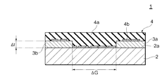
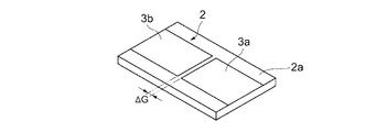
図1は、本発明による静電気対策素子の好ましい実施形態を概略的に示す模式断面図である。この静電気対策素子1は、絶縁性表面2aを有する基体2と、この絶縁性表面2a上に配設された一対の電極3a,3bと、これら電極3a,3bの間に配設された機能層4と、電極3a,3bと電気的に接続された端子電極5(図示せず)と、を備える。この静電気対策素子1において、機能層4は低電圧放電タイプの静電気保護材料として機能し、静電気などの過電圧が印加された際に、この機能層4を介して電極3a,3b間で初期放電が確保されるように設計されている。
(First embodiment)
FIG. 1 is a schematic cross-sectional view schematically showing a preferred embodiment of an antistatic element according to the present invention. The
基体2は、絶縁性表面2aを有する。ここで、絶縁性表面2aを有する基体2とは、絶縁性材料からなる基板の他、基板上の一部に又は全面に絶縁膜が製膜されたものを含む概念である。なお、基体2は、少なくとも電極3a,3b及び機能層4を支持可能なものであれば、その寸法形状は特に制限されない。
The
基体2の具体例としては、例えば、NiZnフェライトやアルミナ、シリカ、マグネシア、窒化アルミ等の誘電率が50以下、好ましくは20以下の低誘電率材料を用いたセラミック基板や単結晶基板等が挙げられる。また、各種公知の基板の表面に、NiZnフェライトやアルミナ、シリカ、マグネシア、窒化アルミ等の誘電率が50以下、好ましくは20以下の低誘電率材料からなる絶縁膜を形成したものも、好適に用いることができる。なお、絶縁膜の形成方法は、特に限定されず、真空蒸着法、反応性蒸着法、スパッタリング法、イオンプレーティング法、CVDやPVD等の気相法等の公知の手法を適用できる。また、基板及び絶縁膜の膜厚は、適宜設定可能である。
Specific examples of the
基体2の絶縁性表面2a上には、一対の電極3a,3bが相互に離間して配設されている。本実施形態では、一対の電極3a,3bは、基体2の平面略中央位置にギャップ距離△Gを置いて、対向配置されている。
On the insulating
電極3a,3bを構成する素材としては、例えば、Cu、Au、Cr、Al、Ag、Zn、W、Mo、Ni、Co、Fe、Pd、Ti及びPt等の金属或いはこれらの合金等が挙げられるが、これらに特に限定されない。電極3a,3bは、放電特性及び耐熱性に優れる高性能な静電気対策素子を実現する観点から、電極を形成する金属材料の抵抗が小さいことが好ましく、具体的には、室温で10×10-8Ωm未満であることが好ましい。このような低抵抗な金属材料としては、特に限定されないが、例えば、Cu(1.7×10-8Ωm)、Au(2.2×10-8Ωm)、Cr(2.6×10⁻⁸Ωm)、Al(2.8×10⁻⁸Ωm)、Ag(1.6×10⁻⁸Ωm)、Zn(5.9×10⁻⁸Ωm)、W(3.5×10⁻⁸Ωm)、Mo(5.1×10⁻⁸Ωm)、Ni(7.2×10⁻⁸Ωm)、Co(7.0×10⁻⁸Ωm)及びFe(9.8×10⁻⁸Ωm)から選ばれる少なくとも一種類の金属或いはこれらの合金が挙げられる。抵抗値は、室温で5×10⁻⁸Ωm未満であることがより好ましい。また、電極3a,3bは、低抵抗で成膜性に優れる電極3a,3bを作製容易である観点から、Cu、Au、Cr、Al及びAgから選ばれる少なくとも一種類の金属或いはこれらの合金であることが特に好ましい。なお、本実施形態では、電極3a,3bは、平面視で矩形状に形成されているが、その形状は特に制限されず、例えば、櫛歯状、或いは、鋸状に形成されていてもよい。電極3a,3bの形成方法(電極3a,3b間のギャップの形成方法)は、特に限定されず、公知の手法を適宜選択することができる。その具体例としては、例えば、レーザ或いはイオンビームによるパターン形成方法や、フォトリソグラフィーを利用したパターン形成方法等が挙げられる。
Examples of the material constituting the
電極3a,3b間のギャップ距離△Gは、低電圧初期放電を確保するとともに、ギャップ形成時の加工容易性を保ちつつ電極3a,3b間の短絡を抑制する観点から、0.5〜10μmの範囲内で設定され、より好ましくは0.5〜8μmである。一方、電極3a,3bの厚み△Tは、放電時の電極3a,3bの破損及び電極間のギャップ距離△Gの変動を抑制して耐久性を高める観点から、△G/△T=1〜30の関係を満たすように設定され、より好ましくは2〜20である。具体的には、電極3a,3b間のギャップ距離△Gによって異なるが、電極3a,3bの厚み△Tは、0.1〜1μmの範囲内で設定することが好ましい。
The gap distance ΔG between the
上記の電極3a,3b間には、機能層4が配設されている。本実施形態では、上述した基体2の絶縁性表面2a上及び電極3a,3b上に、機能層4が積層された構成となっている。この機能層4の寸法形状及びその配設位置は、過電圧が印加された際に自身を介して電極3a,3b間で初期放電が確保されるように設計されている限り、特に限定されない。
A functional layer 4 is disposed between the
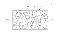
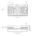
図2は、機能層4の模式平面図である。
機能層4は、絶縁性無機材料4aのマトリックス中に島状の導電性無機材料4bの集合体が不連続に点在した海島構造のコンポジットから構成されている。本実施形態では、機能層4は、逐次スパッタリングを行うことにより形成されている。より具体的には、基体2の絶縁性表面2a上及び/又は電極3a,3b上に、導電性無機材料4bをスパッタリングして部分的に(不完全に)成膜した後、引き続き絶縁性無機材料4aをスパッタリングすることにより、謂わば、島状に点在した導電性無機材料4bの層とこれを覆う絶縁性無機材料4aの層との積層構造のコンポジットが形成されている。
FIG. 2 is a schematic plan view of the functional layer 4.
The functional layer 4 is composed of a composite with a sea-island structure in which aggregates of island-shaped conductive
マトリックスを構成する絶縁性無機材料4aの具体例としては、例えば、金属酸化物、金属窒化物等が挙げられるが、これらに特に限定されない。絶縁性やコスト面を考慮すると、Al2O3、TiO2、SiO2、ZnO、In2O3、NiO、CoO、SnO2、V2O5、CuO、MgO、ZrO2、AlN、BN及びSiCが好ましい。これらは、1種を単独で用いても、2種以上を併用してもよい。これらの中でも、絶縁性マトリックスに高度の絶縁性を付与する観点からは、Al2O3やSiO2等を用いることがより好ましい。一方、絶縁性マトリックスに半導体性を付与する観点からは、TiO2やZnOを用いることがより好ましい。絶縁性マトリックスに半導体性を付与することで、より低い電圧より放電を開始する静電気対策素子を得ることができる。絶縁性マトリックスに半導体性を付与する方法は、特に限定されないが、例えば、これらTiO2やZnOを単独で用いたり、これらを他の絶縁性無機材料4aと併用すればよい。特に、TiO2は、アルゴン雰囲気中でスパッタリングする際に酸素が欠損し易く、電気伝導度が高くなる傾向にあるので、絶縁性マトリックスに半導体性を付与するにはTiO2を用いることが特に好ましい。
Specific examples of the insulating
導電性無機材料4bの具体例としては、例えば、金属、合金、金属酸化物、金属窒化物、金属炭化物、金属ホウ化物等が挙げられるが、これらに特に限定されない。導電性を考慮すると、C、Ni、Cu、Au、Ti、Cr、Ag、Pd及びPt、或いは、これらの合金が好ましい。
Specific examples of the conductive
絶縁性無機材料4a及び導電性無機材料4bの好ましい組み合わせとしては、特に限定されないが、例えば、CuとSiO2の組み合わせ、及び、AuとSiO2の組み合わせが挙げられる。これらの材料で構成された静電気対策素子は、電気的特性に優れるだけでなく、島状の導電性無機材料4bの集合体が不連続に点在した海島構造のコンポジットを高精度且つ容易に形成することができ、加工性やコスト面でも極めて有利である。
A preferable combination of the insulating
機能層4の総厚みは、特に限定されるものではなく、適宜設定することができるが、より一層の薄膜化を達成し、この静電気対策素子1を用いた電子機器のより一層の小型化及び高性能化を実現する観点から、10nm〜10μmであることが好ましく、15nm〜1μmであることがより好ましく、15〜500nmであることがより好ましい。しかも、無機材料からなる厚みが10nm〜1μmの極めて薄いコンポジットは、スパッタリング法や蒸着法等の公知の薄膜形成方法を適用して形成することができるので、これにより、静電気対策素子1の生産性及び経済性が高められる。本実施形態の如く、謂わば、不連続に点在した島状の導電性無機材料4bの層と絶縁性無機材料4aのマトリックスの層とを形成する場合、導電性無機材料4bの層の厚みは、1〜10nmであることが好ましく、絶縁性無機材料4aの層の厚みは、10nm〜10μmであることが好ましく、より好ましくは10nm〜1μmであり、さらに好ましくは10〜500nmである。
The total thickness of the functional layer 4 is not particularly limited and can be set as appropriate. However, the thickness of the functional layer 4 can be further reduced, and the electronic device using the
機能層4の形成方法は、上述したスパッタリング法に限定されるものではない。基体2の絶縁性表面2a上及び/又は電極3a,3b上に、公知の薄膜形成方法を適用して、上述した絶縁性無機材料4a及び導電性無機材料4bを付与することにより、機能層4を形成することができる。すなわち、この静電気対策素子1は、上記従来の印刷法により形成する有機−無機複合膜とは異なり、スパッタリング法や蒸着法等による層形成が適用可能な絶縁性無機材料4aと導電性無機材料4bとのコンポジットを機能層4として採用した点に、格別の優位性を有する。なお、本実施形態の静電気対策素子1は、電極3a,3b間に電圧を印加することにより機能層4中へ電極3a,3bの一部が飛散した結果、機能層4が、電極3a,3bを構成する素材を含む構成であってもよい。
The method for forming the functional layer 4 is not limited to the sputtering method described above. By applying a known thin film forming method on the insulating
本実施形態の静電気対策素子1においては、絶縁性無機材料4aのマトリックス中に不連続に点在した島状の導電性無機材料4bを含む機能層4が、低電圧放電タイプの静電気保護材料として機能する。具体的には、一対の電極3a,3b間に静電気による電圧が印加されたとき、絶縁性無機材料4aのマトリックス中に不連続に島状に点在した導電性無機材料4bによって構成される任意の経路、つまり電極3a,3b間においてエネルギー集中が大きい地点間で放電が発生し、静電気の放電エネルギーは吸収される。高電圧放電を行った場合、放電後の電極や機能層の一部が破壊されることもあるが、不連続に点在した島状に導電性無機材料4bによって多数の電流経路が形成されているため、複数回の静電気吸収が可能である。
In the
とりわけ、本実施形態の静電気対策素子1は、電極3a,3b間のギャップ距離△G及び電極3a,3bの厚み△Tが特定の条件下に制御され、比較的に、ギャップ距離△Gが狭小化されるとともに電極3a,3bの熱容量が大きくなり、放熱が良好となるため、放電開始電圧が低く、また、繰り返し使用時の耐久性が高められたものとなる。
In particular, in the
しかも、本実施形態においては、低電圧放電タイプの静電気保護材料として機能する機能層4として、少なくとも絶縁性無機材料4aと導電性無機材料4bとから構成されるコンポジットが採用されている。そのため、この静電気対策素子1は、上記従来の有機−無機複合膜のものに比して、耐熱性及び耐候性に格別優れたものとなる。その上さらに、スパッタリング法により機能層4が形成されているので、生産性及び経済性に優れたものとなる。
Moreover, in the present embodiment, a composite composed of at least an insulating
なお、上記の第1実施形態の静電気対策素子1においては、絶縁性無機材料4aのマトリックス中に導電性無機材料4bが不連続に分散したコンポジットを機能層4として採用しているが、機能層4として、シリコーン樹脂やエポキシ樹脂等の絶縁性の高い樹脂中に、一例としてAg、Cu、Ni、Al、Feのような金属粒子或いは導電性を有する金属化合物の粒子を分散させたコンポジットを採用することもできる。
In the
(第2実施形態)
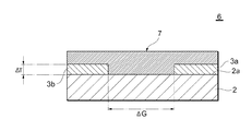
図3は、本発明による静電気対策素子の他の好ましい実施形態を概略的に示す模式断面図である。この静電気対策素子6は、機能層4に代えて機能層7を有する他は、上述した第1実施形態の静電気対策素子1と同じ構成を有する。
(Second Embodiment)
FIG. 3 is a schematic cross-sectional view schematically showing another preferred embodiment of the antistatic element according to the present invention. The
機能層7は、絶縁性無機材料4a(図示せず)のマトリックス中に導電性無機材料4b(図示せず)が不連続に分散したコンポジットである。本実施形態では、機能層7は、基体2の絶縁性表面2a上及び/又は電極3a,3b上に、絶縁性無機材料4aを含むターゲット(又は、絶縁性無機材料4a及び導電性無機材料4bを含むターゲット)を用いてスパッタリング(又は、同時スパッタリング)した後、電極3a,3b間に電圧を印加して電極3a,3bの一部を絶縁性無機材料4a中へランダムに飛散させることにより、形成されている。したがって、本実施形態の機能層7は、導電性無機材料4bとして電極3a,3bを構成する素材を少なくとも含むものとなっている。
The
機能層7の総厚みは、特に限定されるものではなく、適宜設定することができるが、より一層の薄膜化を達成する観点から、10nm〜10μmであることが好ましく、より好ましくは10nm〜1μmであり、さらに好ましくは10〜500nmである。
The total thickness of the
本実施形態の静電気対策素子6においては、低電圧放電タイプの静電気保護材料として機能する機能層7として、絶縁性無機材料4aのマトリックス中に粒子状の導電性無機材料4bが不連続に分散したコンポジットが採用されている。このように構成しても、上記第1実施形態と同様の作用効果が奏される。
In the
(第3実施形態)
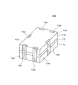
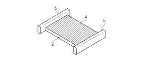
図4は、本発明による複合電子部品の好ましい実施形態の外観構成を概略的に示す斜視図である。
(Third embodiment)
FIG. 4 is a perspective view schematically showing an external configuration of a preferred embodiment of the composite electronic component according to the present invention.
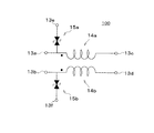
図4に示すように、本実施形態による複合電子部品100は、静電気保護機能を備えた薄膜コモンモードフィルタであって、第1及び第2の磁性基体11a、11bと、第1の磁性基体11aと第2の磁性基体11bに挟まれた複合機能層12とを備えている。また、第1の磁性基体11a、複合機能層12及び第2の磁性基体11bからなる積層体の外周面には、第1〜第6の端子電極13a〜13fが形成されている。このうち、第1及び第2の端子電極13a,13bは第1の側面10aに形成され、第3及び第4の端子電極13c、13dは第1の側面10aと対向する第2の側面10bに形成され、第5の端子電極13eは第1及び第2の側面10a,10bと直交する第3の側面10cに形成され、第6の端子電極13fは第3の側面と対向する第4の側面10dに形成されている。
As shown in FIG. 4, the composite
第1及び第2の磁性基体11a,11bは、複合機能層12を物理的に保護すると共に、コモンモードフィルタの閉磁路としての役割を果たすものである。第1及び第2の磁性基体11a,11bの材料としては、焼結フェライト、複合フェライト(粉状のフェライトを含有した樹脂)等を用いることができる。
The first and second
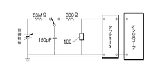
図5は、複合電子部品100の構成を示す回路図である。
FIG. 5 is a circuit diagram illustrating a configuration of the composite
図5に示すように、複合電子部品100は、コモンモードチョークコイルとして機能するインダクタ素子14a、14bと、静電気対策素子15a、15bとを備えており、インダクタ素子14a、14bの一端は第1及び第2の端子電極13a,13bにそれぞれ接続され、他端は第3及び第4の端子電極13c、13dにそれぞれ接続されている。また、静電気対策素子15a,15bの一端は第1及び第2の端子電極13a,13bにそれぞれ接続され、他端は第5及び第6の端子電極13e,13fにそれぞれ接続されている。この複合電子部品100は、一対の信号ライン上に実装される際、第1及び第2の端子電極13a,13bは信号ラインの入力側に接続され、第3及び第4の端子電極13c,13dは信号ラインの出力側に接続される。また、第5及び第6の端子電極13e,13fはグランドラインに接続される。
As shown in FIG. 5, the composite
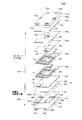
図6は、複合電子部品100の層構造の一例を示す分解斜視図である。
FIG. 6 is an exploded perspective view showing an example of the layer structure of the composite
図6に示すように、複合電子部品100は、第1及び第2の磁性基体11a、11bと、第1及び第2の磁性基体11a、11bに挟まれた複合機能層12とを備えており、複合機能層12はコモンモードフィルタ層12aと静電気対策素子層12bによって構成されている。
As shown in FIG. 6, the composite
コモンモードフィルタ層12aは、絶縁層16a〜16eと、磁性層16fと、接着層16gと、絶縁層16b上に形成された第1のスパイラル導体17と、絶縁層16c上に形成された第2のスパイラル導体18と、絶縁層16a上に形成された第1の引き出し導体19と、絶縁層16d上に形成された第2の引き出し導体20とを備えている。
The common
絶縁層16a〜16eは、各導体パターン間、或いは導体パターンと磁性層16fとを絶縁すると共に、導体パターンが形成される下地面の平坦性を確保する役割を果たす。絶縁層16a〜16eの材料としては、電気的及び磁気的な絶縁性に優れ、加工性のよい樹脂を用いることが好ましく、ポリイミド樹脂やエポキシ樹脂を用いることが好ましい。導体パターンとしては、導電性及び加工性に優れたCu、Al等を用いることが好ましい。導体パターンの形成は、フォトリソグラフィーを用いたエッチング法やアディティブ法(めっき)により行うことができる。
The insulating
絶縁層16a〜16eの中央領域であって第1及び第2のスパイラル導体17,18の内側には、絶縁層16a〜16eを貫通する開口25が設けられており、開口25の内部には、第1の磁性基体11aと第2の磁性基体11bとの間に閉磁路を形成するための磁性体26が充填されている。磁性体26としては、複合フェライト等を用いることが好ましい。
An
さらに、絶縁層16eの表面には磁性層16fが形成されている。開口25内の磁性体26は、複合フェライト(磁性粉含有樹脂)のペーストを硬化させて形成しているが、硬化時に樹脂の収縮が発生し、開口部分に凹凸が生じる。この凹凸をできるだけ少なくするためには、開口25の内部のみならず絶縁層16eの表面全体にもペーストを塗布することが好ましく、磁性層16fはそのような平坦性の確保を目的として形成される。
Further, a
接着層16gは磁性基体11bを磁性層16f上に貼り付けるために必要な層である。また、磁性基体11b及び磁性層16fの表面の凹凸を緩和し、密着性を高める役割を果たす。特に限定されるものではないが、接着層16gの材料としては、エポキシ樹脂、ポリイミド樹脂、ポリアミド樹脂等を用いることができる。
The
第1のスパイラル導体17は、図5に示したインダクタ素子14aに対応するものである。第1のスパイラル導体17の内周端は、絶縁層16bを貫通する第1のコンタクトホール導体21及び第1の引き出し導体19を介して、第1の端子電極13aに接続されている。また、第1のスパイラル導体17の外周端は、第3の引き出し導体23を介して第3の端子電極13cに接続されている。
The
第2のスパイラル導体18は、図5に示したインダクタ素子14bに対応するものである。第2のスパイラル導体18の内周端は、絶縁層16dを貫通する第2のコンタクトホール導体22及び第2の引き出し導体20を介して、第2の端子電極13bに接続されている。また、第2のスパイラル導体18の外周端は、第4の引き出し導体24を介して第4の端子電極13dに接続されている。
The
第1及び第2のスパイラル導体17,18は共に同一の平面形状を有しており、しかも平面視で同じ位置に設けられている。第1及び第2のスパイラル導体17,18は完全に重なり合っていることから、両者の間には強い磁気結合が生じている。以上の構成により、コモンモードフィルタ層12a内の導体パターンはコモンモードフィルタを構成している。
Both the first and
静電気対策素子層12bは、下地絶縁層27と、下地絶縁層27の表面に形成された第1及び第2のギャップ電極28,29と、第1及び第2のギャップ電極28,29を覆う静電気吸収層30とを備えている。第1のギャップ電極28付近の層構造は、図5に示した第1の静電気対策素子15aとして機能する部分であり、第2のギャップ電極29付近の層構造は、第2の静電気対策素子15bとして機能する部分である。第1のギャップ電極28の一端は第1の端子電極13aに接続されており、他端は第5の端子電極13eに接続されている。また、第2のギャップ電極29の一端は第2の端子電極13bに接続されており、他端は第6の端子電極13fに接続されている。
The
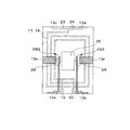
図7は、ギャップ電極28,29と他の導体パターンとの位置関係を示す略平面図である。
FIG. 7 is a schematic plan view showing the positional relationship between the
図7に示すように、ギャップ電極28,29が有するギャップ28G,29Gは、コモンモードフィルタを構成する第1及び第2のスパイラル導体17,18及び第1及び第2の引き出し導体19,20と平面的に重ならない位置に設けられている。特に限定されるものではないが、本実施形態においては、スパイラル導体17,18の内側であって、スパイラル導体17,18と開口25との間の空き領域にギャップ28G,29Gが設けられている。詳細は後述するが、静電気対策素子は静電気の吸収によって部分的に破損、変形するため、静電気対策素子と重なる位置に導体パターンが配置されている場合にはそれらも一緒に破損するおそれがある。しかし、静電気対策素子のギャップ28G,29Gが導体パターンを避けた位置に設けられていることから、静電気によって破壊されたときの上下層の影響を抑えることができ、より信頼性の高い複合電子部品を実現することができる。
As shown in FIG. 7, the
図8(a)及び(b)は、静電気対策素子層12bにおける第1のギャップ電極28付近の層構造の一例を示す図であって、(a)は略平面図、(b)は略断面図である。なお、第2のギャップ電極29の構成は第1のギャップ電極28と同一であるため、重複する説明を省略する。
8A and 8B are views showing an example of a layer structure in the vicinity of the
静電気対策素子層12bは、磁性基体11aの表面に形成された下地絶縁層27と、第1のギャップ電極28を構成する一対の電極28a,28bと、これらの電極28a,28bの間に配設された静電気吸収層30とを備えている。
The
下地絶縁層27は、上述した第1実施形態における絶縁性表面2aとして機能するものである。下地絶縁層27は絶縁性材料からなり、本実施形態においては製造上の容易さから磁性基体11aの全面を覆っているが、少なくとも電極28a,28b及び静電気吸収層30の下地となっていればよく、必ずしも全面を覆う必要はない。下地絶縁層27の具体例としては、NiZnフェライトやアルミナ、シリカ、マグネシア、窒化アルミ等の誘電率が50以下、好ましくは20以下の低誘電率材料を製膜したものの他、各種公知の基板の表面にこれらの低誘電率材料からなる絶縁膜を製膜したものも、好適に用いることができる。なお、下地絶縁層27の製膜方法は、特に限定されず、真空蒸着法、反応性蒸着法、スパッタリング法、イオンプレーティング法、CVDやPVD等の気相法等の公知の手法を適用できる。また、下地絶縁層27の膜厚は、適宜設定可能である。
The
電極28a,28bは、上述した第1実施形態における電極3a,3bに相当するものであり、重複する説明は省略する。なお、電極28a,28b間のギャップ距離△Gとギャップ電極28の厚み△Tは、上述した第1実施形態における電極3a,3b間のギャップ距離△G及び電極3a,3bの厚み△Tの関係と同様に設定されている。
The
静電気吸収層30は、絶縁性無機材料32のマトリックス中に島状の導電性無機材料33の集合体が不連続に点在した海島構造のコンポジットから構成されている。この静電気吸収層30は、上述した第1実施形態における機能層4に相当し、また、絶縁性無機材料32及び導電性無機材料33は、上述した第1実施形態における絶縁性無機材料4a及び導電性無機材料4bに相当するものであり、それらの重複する説明は省略する。
The
この静電気対策素子層12bにおいて、静電気吸収層30は低電圧放電タイプの静電気保護材料として機能し、静電気などの過電圧が印加された際に、この静電気吸収層30を介して電極28a,28b間で初期放電が確保されるように設計されている。また、本実施形態の絶縁性無機材料32は、上層に位置する任意の層(例えば絶縁層16a)から一対の電極28a,28bや導電性無機材料33を保護する保護層としても機能する。
In the
以上説明したように、本実施形態による複合電子部品100は、静電容量が小さく、放電開始電圧が低く、且つ、繰り返し使用時の耐久性に優れた低電圧タイプの静電気対策素子を内蔵しているので、高性能な静電気保護機能を備えたコモンモードフィルタとして機能する複合電子部品を実現することができる。
As described above, the composite
また、本実施形態によれば、静電気対策素子層12bの材料として絶縁性無機材料32及び導電性無機材料33が使用され、静電気対策素子層12bを構成する各種材料に樹脂が含まれていないことから、磁性基体11a上に静電気対策素子層12bを形成し、さらにその上にコモンモードフィルタ層12aを形成することができる。コモンモードフィルタ層12aをいわゆる薄膜工法で形成する場合には350℃以上、導体パターンが形成されたセラミックシートを順次積層するいわゆる積層工法で形成する場合には800℃の熱処理工程が必要となるが、静電気対策素子層の材料として絶縁性無機材料32及び導電性無機材料33を使用した場合には、熱処理工程に耐えることができ、正常に機能する静電気対策素子を確実に形成することができる。さらに、磁性基体上の十分に平坦な面に静電気対策素子を形成することができ、ギャップ電極の微小なギャップを安定的に形成することができる。
Further, according to the present embodiment, the insulating
また、本実施形態によれば、ギャップ電極の形成位置がコモンモードフィルタを構成する第1及び第2のスパイラル導体等と平面的に重ならず、それらの導体パターンを避けた位置に設けられていることから、静電気対策素子が静電気によって部分的に破壊されたときの上下方向の影響を抑えることができ、より信頼性の高い複合電子部品を実現することができる。 Further, according to the present embodiment, the gap electrode formation position does not overlap with the first and second spiral conductors etc. constituting the common mode filter in a plane, and is provided at a position avoiding those conductor patterns. Therefore, the influence in the vertical direction when the anti-static element is partially destroyed by static electricity can be suppressed, and a more reliable composite electronic component can be realized.
さらに、本実施形態によれば、図5に示したように、複合電子部品100は一対の信号ライン上に実装され、静電気対策素子15a,15bは、コモンモードフィルタよりも信号ラインの入力側に設けられていることから、静電気対策素子による過電圧の吸収効率を高めることができる。通常、静電気による過電圧は、インピーダンス整合のとれていない異常な電圧であるため、コモンモードフィルタの入力端で一回反射する。この反射信号は元の信号波形に重畳され、電圧が上昇した信号は、静電気対策素子で一気に吸収される。すなわち、静電気対策素子の後段にあるコモンモードフィルタが元波形よりも大きい波形にしてくれるので、電圧レベルが低い状態から吸収する場合よりも静電気対策素子で吸収されやすい状態を作り出すことができる。こうして、一回吸収した信号をコモンモードフィルタに入力することにより、細かいノイズを除去することができる。
Furthermore, according to the present embodiment, as shown in FIG. 5, the composite
以下、実施例により本発明を詳細に説明するが、本発明はこれらに限定されるものではない。 EXAMPLES Hereinafter, although an Example demonstrates this invention in detail, this invention is not limited to these.
(実施例1)
図9に示すように、まず、絶縁性の基体2(NiZnフェライト基板、誘電率:13、TDK株式会社製)の一方の絶縁性表面2a上に、スパッタリング法により、下地層(密着層)として厚み10nmのクロム薄膜を形成し、その後、このクロム薄膜上に、スパッタリング法により、厚み0.1μmのCu薄膜を略全面に形成することにより、クロムと銅の2層構造からなる金属薄膜を形成した。次に、形成されたCu薄膜の上面に、ロールコーターを用いてネガ型フォトレジストをベタ塗布した後、これを温度95℃及び3〜15分の条件下で乾燥させ、厚み2〜6μmのレジスト層を形成した。その後、電極間のギャップに相当する部分のみをマスクした状態で、露光処理を行ない、電極間のギャップに相当する部分以外を硬化させ、未露光部分のレジスト層を現像除去した。次いで、露出したCu薄膜(電極間のギャップに相当する部分)を、イオンミリングによりエッチングすることにより、相互に離間して対向配置された一対の帯状の電極3a,3bを形成した。このとき、電極3a,3b間のギャップ距離△Gは、1μmとした。
Example 1
As shown in FIG. 9, first, on one insulating
次いで、図10に示すように、上記の基体2の絶縁性表面2a上及び電極3a,3b上に、以下の手順で機能層4を形成した。
Next, as shown in FIG. 10, the functional layer 4 was formed on the insulating
まず、基体2の電極3a,3bが形成された面側に、スパッタリング法でAuを部分的に成膜することにより、厚み3nmのAu薄膜が島状に不連続に点在した導電性無機材料4bの層を形成した。このスパッタリングは、マルチターゲットスパッタ装置(商品名:ES350SU、株式会社エイコー・エンジニアリング製)を使用し、アルゴン圧力が10mTorr、投入電力が20W、スパッタ時間が40秒の条件下で実施した。
First, a conductive inorganic material in which Au thin films having a thickness of 3 nm are scattered in an island shape discontinuously by depositing Au partially on the surface of the
次に、電極3a,3b及び導電性無機材料4bの層を厚み方向において完全に覆うように、基体2の電極3a,3b及び導電性無機材料4bの層が形成された面側に、スパッタリング法で二酸化ケイ素を略全面に成膜することにより、厚み600nmの絶縁性無機材料4aの層を形成した。このスパッタリングは、マルチターゲットスパッタ装置(商品名:ESU350、株式会社エイコー・エンジニアリング製)を使用し、アルゴン圧力が10mTorr、投入電力が400W、スパッタ時間が40分の条件下で実施した。
Next, a sputtering method is applied to the surface of the
以上の操作により、絶縁性無機材料4aのマトリックス中で不連続に点在した島状の導電性無機材料4bを有する機能層4が形成された。その後、図11に示すように、電極3a,3bの外周端部に接続するように、Cuを主成分とする端子電極5を形成することにより、実施例1の静電気対策素子1を得た。
By the above operation, the functional layer 4 having the island-shaped conductive
(実施例2)
電極3a,3bの厚みを0.2μmに変更すること以外は、実施例1と同様に操作して、実施例2の静電気対策素子1を得た。
(Example 2)
Except for changing the thickness of the
(実施例3)
電極3a,3bの厚みを0.4μmに変更すること以外は、実施例1と同様に操作して、実施例3の静電気対策素子1を得た。
(Example 3)
Except changing the thickness of
(実施例4)
電極3a,3b間のギャップ距離△Gを2μmに変更すること以外は、実施例3と同様に操作して、実施例4の静電気対策素子1を得た。
Example 4
The
(実施例5)
電極3a,3b間のギャップ距離△Gを2.5μmに変更すること以外は、実施例1と同様に操作して、実施例5の静電気対策素子1を得た。
(Example 5)
An
(比較例1)
電極3a,3b間のギャップ距離△Gを5μmに変更し、機能層4の形成を省略すること以外は、実施例1と同様に操作して、比較例1の静電気対策素子1を得た。
(Comparative Example 1)
An
(比較例2)
電極3a,3b間のギャップ距離△Gを5μmに変更し、機能層4の形成時の導電性無機材料4bのスパッタリングを省略すること以外は、実施例1と同様に操作して、比較例2の静電気対策素子1を得た。
(Comparative Example 2)
Comparative Example 2 was carried out in the same manner as in Example 1 except that the gap distance ΔG between the
(比較例3)
電極3a,3b間のギャップ距離△Gを5μmに変更すること以外は、実施例1と同様に操作して、比較例3の静電気対策素子を得た。
(Comparative Example 3)
A static electricity countermeasure element of Comparative Example 3 was obtained in the same manner as in Example 1 except that the gap distance ΔG between the
(比較例4)
電極3a,3b間のギャップ距離△Gを3.5μmに変更すること以外は、実施例1と同様に操作して、比較例4の静電気対策素子を得た。
(Comparative Example 4)
A static electricity countermeasure element of Comparative Example 4 was obtained in the same manner as in Example 1 except that the gap distance ΔG between the
<静電気放電試験>
次に、上記のようにして得られた実施例1〜3並びに比較例1〜3の静電気対策素子について、図12に示す静電気試験回路を用いて、静電気放電試験を実施した。
<Electrostatic discharge test>
Next, an electrostatic discharge test was performed on the antistatic elements of Examples 1 to 3 and Comparative Examples 1 to 3 obtained as described above using the electrostatic test circuit shown in FIG.
この静電気放電試験は、国際規格IEC61000−4−2の静電気放電イミュニティ試験及びノイズ試験に基づき、人体モデルに準拠(放電抵抗330Ω、放電容量150pF、印加電圧8kV、接触放電)して行った。具体的には、図12の静電気試験回路に示すように、評価対象の静電気対策素子の一方の端子電極をグランドに接地するとともに、他方の端子電極に静電気パルス印加部を接続した後、静電気パルス印加部に放電ガンを接触させて静電気パルスを印加した。ここで印加する静電気パルスは、放電開始電圧以上の電圧を印加した。 This electrostatic discharge test was performed in accordance with a human body model (discharge resistance 330Ω, discharge capacity 150 pF, applied voltage 8 kV, contact discharge) based on the electrostatic discharge immunity test and noise test of the international standard IEC61000-4-2. Specifically, as shown in the electrostatic test circuit of FIG. 12, one terminal electrode of the electrostatic countermeasure element to be evaluated is grounded, and an electrostatic pulse applying unit is connected to the other terminal electrode, An electrostatic pulse was applied by bringing a discharge gun into contact with the application section. The electrostatic pulse applied here applied a voltage higher than the discharge start voltage.
なお、放電開始電圧は、静電気試験を0.4kVから0.2kV間隔で増加させながら行なった際に観測される静電気吸収波形において、静電気吸収効果が現れた電圧とする。また、ピーク電圧は、IEC61000−4−2に基づく静電気試験を充電電圧8kVの接触放電で行なった際における、静電気パルスの最大電圧値とする。さらに、クランプ電圧は、IEC61000−4−2に基づく静電気試験を充電電圧8kVの接触放電で行なった際における、静電気パルスの波頭値から30ナノ秒後の電圧値とする。
The discharge start voltage is a voltage at which an electrostatic absorption effect appears in an electrostatic absorption waveform observed when the electrostatic test is performed while increasing the interval from 0.4 kV to 0.2 kV. The peak voltage is the maximum voltage value of the electrostatic pulse when the electrostatic test based on IEC61000-4-2 is performed with the contact discharge at the charging voltage of 8 kV. Further, the clamp voltage is a
なお、静電容量は、1MHzにおける静電容量(pF)を測定した。また、放電耐性は、静電気放電試験を繰り返し実施して、静電気対策素子が機能しなくなる回数を測定し、その回数の大小により評価した。表1に、評価結果を示す。 In addition, the electrostatic capacitance measured the electrostatic capacitance (pF) in 1 MHz. In addition, the discharge resistance was evaluated by measuring the number of times that the anti-static element did not function by repeatedly carrying out an electrostatic discharge test and evaluating the number of times. Table 1 shows the evaluation results.
(実施例6〜8)
電極3a,3bの作製時に使用する金属をCuに代えてAg、Au、Alに変更すること以外は、実施例3と同様に操作して、実施例6〜8の静電気対策素子1を得た。表2に、評価結果を示す。
(Examples 6 to 8)
The
以上説明した通り、本発明の静電気対策素子及びその複合電子部品は、放電開始電圧が低く、且つ、繰り返しの使用の耐久性が高められており、その上さらに、耐熱性及び耐候性の向上、さらなる薄膜化、並びに、生産性及び経済性の向上が可能なので、各種電子・電気デバイス及びそれらを備える各種機器、設備、システム等に広く且つ有効に利用可能であり、とりわけ、高速差動伝送ライン信号ラインや映像信号ラインにおけるノイズ対策として広く且つ有効に利用可能である。 As described above, the anti-static element and the composite electronic component of the present invention have a low discharge start voltage and enhanced durability for repeated use, and further, improved heat resistance and weather resistance. Since it is possible to further reduce the film thickness and improve productivity and economy, it can be used widely and effectively in various electronic / electrical devices and various equipment, facilities, and systems equipped with them, especially high-speed differential transmission lines. It can be used widely and effectively as a noise countermeasure in signal lines and video signal lines.
1…静電気対策素子、2…基体、2a…絶縁性表面、3a,3b・・・電極、4…機能層、4a…絶縁性無機材料、4b…導電性無機材料、6…静電気対策素子、7…機能層、△G…ギャップ距離、△T…電極の厚み、11a,11b…磁性基体、12…複合機能層(機能層)、12a…コモンモードフィルタ層、12b…静電気対策素子層、14a,14b…インダクタ素子、15a,15b…静電気対策素子、17,18…スパイラル導体、16a〜16e…絶縁層、27…下地絶縁層、28a,28b,29a,29b…電極、30…静電気吸収層(機能層)、32…絶縁性無機材料、33…導電性無機材料、100…複合電子部品。
DESCRIPTION OF
Claims (6)
前記機能層は、絶縁性無機材料のマトリックス中に導電性無機材料が不連続に分散したコンポジットであり、且つ、スパッタリング法によって形成されたものであり、
前記電極間のギャップ距離ΔGが、0.5〜10μm(但し、3.5μm以上の場合を除く。)であり、
前記電極の厚みΔTが、ΔG/ΔT=1〜30の関係を満たす、
静電気対策素子。 A substrate having an insulating surface; electrodes disposed opposite to each other on the insulating surface; and at least a functional layer disposed between the electrodes;
The functional layer is a composite in which a conductive inorganic material is discontinuously dispersed in a matrix of an insulating inorganic material, and is formed by a sputtering method.
The gap distance ΔG between the electrodes is 0.5 to 10 μm (except when it is 3.5 μm or more) ,
The electrode thickness ΔT satisfies a relationship of ΔG / ΔT = 1 to 30,
Antistatic element.
請求項1に記載の静電気対策素子。 The insulating inorganic material is made of Al 2 O 3 , TiO 2 , SiO 2 , ZnO, In 2 O 3 , NiO, CoO, SnO 2 , V 2 O 5 , CuO, MgO, ZrO 2 , AlN, BN, and SiC. At least one selected from the group consisting of:
The antistatic element according to claim 1 .
請求項1又は2に記載の静電気対策素子。 The conductive inorganic material is at least one metal selected from the group consisting of C, Ni, Cu, Au, Ti, Cr, Ag, Pd and Pt, or a metal compound thereof.
The antistatic element according to claim 1 or 2 .
請求項1〜3のいずれか一項に記載の静電気対策素子。 The electrode is at least one metal selected from Cu, Au, Cr, Al, Ag, Zn, W, Mo, Ni, Co, and Fe, or an alloy thereof.
The static electricity countermeasure element as described in any one of Claims 1-3 .
前記インダクタ素子は、樹脂からなる絶縁層と、前記絶縁層上に形成された導体パターンとを備え、
前記静電気対策素子は、前記磁性基体上に形成された下地絶縁層と、該下地絶縁層上において相互に離間して対向配置された電極と、少なくとも該電極間に配置された機能層とを備え、
前記機能層は、絶縁性無機材料のマトリックス中に導電性無機材料が不連続に分散したコンポジットであり、且つ、スパッタリング法によって形成されたものであり、
前記電極間のギャップ距離ΔGが、0.5〜10μm(但し、3.5μm以上の場合を除く。)であり、
前記電極の厚みΔTが、ΔG/ΔT=1〜30の関係を満たす、
複合電子部品。 A composite electronic component having an inductor element and an anti-static element between two magnetic substrates,
The inductor element includes an insulating layer made of resin, and a conductor pattern formed on the insulating layer,
The electrostatic protection element includes a base insulating layer formed on the magnetic substrate, electrodes disposed opposite to each other on the base insulating layer, and a functional layer disposed at least between the electrodes. ,
The functional layer is a composite in which a conductive inorganic material is discontinuously dispersed in a matrix of an insulating inorganic material, and is formed by a sputtering method.
The gap distance ΔG between the electrodes is 0.5 to 10 μm (except when it is 3.5 μm or more) ,
The electrode thickness ΔT satisfies a relationship of ΔG / ΔT = 1 to 30,
Composite electronic components.
前記コモンモードフィルタ層は、
樹脂からなる第1及び第2の絶縁層と、
前記第1の絶縁層上に形成された第1のスパイラル導体と、
前記第2の絶縁層上に形成された第2のスパイラル導体とを備え、
前記静電気対策素子層は、
前記第1のスパイラル導体の一端に接続された第1の静電気対策素子と、
前記第2のスパイラル導体の一端に接続された第2の静電気対策素子とを備え、
前記第1及び第2のスパイラル導体は、積層方向と垂直な平面にそれぞれ形成され、互いに磁気結合するように配置され、
前記第1及び第2の静電気対策素子は、前記磁性基体上に形成された下地絶縁層と、該下地絶縁層上において相互に離間して対向配置された電極と、少なくとも該電極間に配置された機能層と備え、
前記機能層は、絶縁性無機材料のマトリックス中に導電性無機材料が不連続に分散したコンポジットであり、且つ、スパッタリング法によって形成されたものであり、
前記電極間のギャップ距離ΔGが、0.5〜10μm(但し、3.5μm以上の場合を除く。)であり、
前記電極の厚みΔTが、ΔG/ΔT=1〜30の関係を満たす、
複合電子部品。 A common mode filter layer and an anti-static element layer provided between two magnetic substrates;
The common mode filter layer is
First and second insulating layers made of resin;
A first spiral conductor formed on the first insulating layer;
A second spiral conductor formed on the second insulating layer,
The anti-static element layer is
A first antistatic element connected to one end of the first spiral conductor;
A second antistatic element connected to one end of the second spiral conductor,
The first and second spiral conductors are respectively formed in planes perpendicular to the stacking direction, and are arranged so as to be magnetically coupled to each other.
The first and second antistatic elements are disposed between a base insulating layer formed on the magnetic substrate, electrodes disposed opposite to each other on the base insulating layer, and at least between the electrodes. With a functional layer
The functional layer is a composite in which a conductive inorganic material is discontinuously dispersed in a matrix of an insulating inorganic material, and is formed by a sputtering method.
The gap distance ΔG between the electrodes is 0.5 to 10 μm (except when it is 3.5 μm or more) ,
The electrode thickness ΔT satisfies a relationship of ΔG / ΔT = 1 to 30,
Composite electronic components.
Priority Applications (3)
| Application Number | Priority Date | Filing Date | Title |
|---|---|---|---|
| JP2009248089A JP5196330B2 (en) | 2008-12-18 | 2009-10-28 | Electrostatic countermeasure element and its composite electronic parts |
| US12/654,210 US8199451B2 (en) | 2008-12-18 | 2009-12-14 | ESD protection device and composite electronic component of the same |
| KR1020090124857A KR20100070997A (en) | 2008-12-18 | 2009-12-15 | Esd protection device and composite electronic component of the same |
Applications Claiming Priority (3)
| Application Number | Priority Date | Filing Date | Title |
|---|---|---|---|
| JP2008322433 | 2008-12-18 | ||
| JP2008322433 | 2008-12-18 | ||
| JP2009248089A JP5196330B2 (en) | 2008-12-18 | 2009-10-28 | Electrostatic countermeasure element and its composite electronic parts |
Publications (2)
| Publication Number | Publication Date |
|---|---|
| JP2010165665A JP2010165665A (en) | 2010-07-29 |
| JP5196330B2 true JP5196330B2 (en) | 2013-05-15 |
Family
ID=42265713
Family Applications (1)
| Application Number | Title | Priority Date | Filing Date |
|---|---|---|---|
| JP2009248089A Active JP5196330B2 (en) | 2008-12-18 | 2009-10-28 | Electrostatic countermeasure element and its composite electronic parts |
Country Status (3)
| Country | Link |
|---|---|
| US (1) | US8199451B2 (en) |
| JP (1) | JP5196330B2 (en) |
| KR (1) | KR20100070997A (en) |
Families Citing this family (17)
| Publication number | Priority date | Publication date | Assignee | Title |
|---|---|---|---|---|
| US8422190B2 (en) * | 2008-09-30 | 2013-04-16 | Tdk Corporation | Composite electronic device, manufacturing method thereof, and connection structure of composite electronic device |
| JP5196330B2 (en) * | 2008-12-18 | 2013-05-15 | Tdk株式会社 | Electrostatic countermeasure element and its composite electronic parts |
| JP4835699B2 (en) * | 2009-01-22 | 2011-12-14 | Tdk株式会社 | High-speed digital transmission circuit |
| JP4749482B2 (en) * | 2009-07-08 | 2011-08-17 | Tdk株式会社 | Composite electronic components |
| JP2012074228A (en) * | 2010-09-28 | 2012-04-12 | Tdk Corp | Static-electricity countermeasure element |
| JP2013175443A (en) * | 2012-01-27 | 2013-09-05 | Tdk Corp | Static electricity countermeasure element |
| KR101792269B1 (en) * | 2012-04-05 | 2017-11-01 | 삼성전기주식회사 | Electronic component and method for manufacturing the same |
| KR101771726B1 (en) * | 2012-06-18 | 2017-08-25 | 삼성전기주식회사 | Electrostatic discharge protection device and composite electronic elements comprising the same |
| JP5784688B2 (en) | 2012-12-10 | 2015-09-24 | サムソン エレクトロ−メカニックス カンパニーリミテッド. | Electrostatic discharge structure and method for manufacturing electrostatic discharge structure |
| KR101719841B1 (en) * | 2012-12-10 | 2017-03-24 | 삼성전기주식회사 | Common mode filter |
| KR101912270B1 (en) * | 2013-07-26 | 2018-10-29 | 삼성전기 주식회사 | Common mode filter |
| US9293913B2 (en) * | 2013-08-01 | 2016-03-22 | Tdk Corporation | ESD protection component and method for manufacturing ESD protection component |
| KR101983159B1 (en) * | 2013-11-28 | 2019-05-28 | 삼성전기주식회사 | Coil component and and method of manufacturing the same |
| KR20160024262A (en) * | 2014-08-25 | 2016-03-04 | 삼성전기주식회사 | Common mode filter and manufacturing method thereof |
| WO2017038238A1 (en) * | 2015-09-01 | 2017-03-09 | 株式会社村田製作所 | Esd protection element |
| CN105810677B (en) | 2016-05-16 | 2019-01-29 | 京东方科技集团股份有限公司 | Electrostatic discharge assembly, array substrate and preparation method thereof, and display panel |
| CN113363098A (en) * | 2021-03-30 | 2021-09-07 | 中国石油大学(华东) | Self-extinguishing arc discharge switch structure for underground operation |
Family Cites Families (22)
| Publication number | Priority date | Publication date | Assignee | Title |
|---|---|---|---|---|
| US2924734A (en) * | 1955-06-09 | 1960-02-09 | Siemens Ag | Spark gap device |
| US3704388A (en) * | 1970-07-06 | 1972-11-28 | Asea Ab | Spark gap for surge diverters |
| GB1358043A (en) * | 1970-07-21 | 1974-06-26 | Atomic Energy Authority Uk | Electrical spark gap switch apparatus |
| DE2528174C3 (en) * | 1975-06-24 | 1978-06-22 | Hans Dipl.-Phys. Dr. 7000 Stuttgart Salzmann | Laser with traveling wave excitation |
| US6191928B1 (en) | 1994-05-27 | 2001-02-20 | Littelfuse, Inc. | Surface-mountable device for protection against electrostatic damage to electronic components |
| JP3455011B2 (en) * | 1996-05-07 | 2003-10-06 | アルプス電気株式会社 | Surge absorber and method of manufacturing the same |
| JP3817995B2 (en) * | 1999-11-30 | 2006-09-06 | 三菱マテリアル株式会社 | Surge absorbing element and manufacturing method thereof |
| DE20020771U1 (en) * | 2000-02-22 | 2001-02-15 | Dehn & Soehne | Pressure proof encapsulated spark gap arrangement for leading off damaging disturbance variables due to overvoltages, has two opposing electrodes |
| DE60136989D1 (en) * | 2000-02-29 | 2009-01-29 | Ngk Spark Plug Co | spark plug |
| JP2002015831A (en) | 2000-06-30 | 2002-01-18 | Mitsubishi Materials Corp | Chip type surge absorber and method of manufacturing the same |
| JP3900104B2 (en) * | 2003-04-10 | 2007-04-04 | 松下電器産業株式会社 | Antistatic parts |
| JP4725343B2 (en) * | 2006-02-07 | 2011-07-13 | パナソニック株式会社 | Composite electronic component and manufacturing method thereof |
| JP2007242404A (en) | 2006-03-08 | 2007-09-20 | Mitsubishi Materials Corp | surge absorber |
| JP2007265713A (en) | 2006-03-28 | 2007-10-11 | Matsushita Electric Ind Co Ltd | Electrostatic protective material paste and antistatic parts using the same |
| KR100813195B1 (en) | 2006-04-20 | 2008-03-13 | 주식회사 이노칩테크놀로지 | Electrostatic protection device |
| US7733620B2 (en) * | 2006-07-19 | 2010-06-08 | Ta-I Technology Co., Ltd | Chip scale gas discharge protective device and fabrication method of the same |
| TW200816232A (en) * | 2006-09-28 | 2008-04-01 | Inpaq Technology Co Ltd | Material of an over voltage protection device, over voltage protection device and manufacturing method thereof |
| JP2007048759A (en) | 2006-10-18 | 2007-02-22 | Mitsubishi Materials Corp | surge absorber |
| WO2008053717A1 (en) * | 2006-10-31 | 2008-05-08 | Panasonic Corporation | Anti-static part and its manufacturing method |
| TWI377755B (en) * | 2008-11-28 | 2012-11-21 | Cyntec Co Ltd | Over-voltage protecting device and method for making thereof |
| JP5339051B2 (en) * | 2008-12-18 | 2013-11-13 | Tdk株式会社 | Electrostatic countermeasure element and its composite electronic parts |
| JP5196330B2 (en) * | 2008-12-18 | 2013-05-15 | Tdk株式会社 | Electrostatic countermeasure element and its composite electronic parts |
-
2009
- 2009-10-28 JP JP2009248089A patent/JP5196330B2/en active Active
- 2009-12-14 US US12/654,210 patent/US8199451B2/en active Active
- 2009-12-15 KR KR1020090124857A patent/KR20100070997A/en not_active Ceased
Also Published As
| Publication number | Publication date |
|---|---|
| JP2010165665A (en) | 2010-07-29 |
| US8199451B2 (en) | 2012-06-12 |
| US20100157501A1 (en) | 2010-06-24 |
| KR20100070997A (en) | 2010-06-28 |
Similar Documents
| Publication | Publication Date | Title |
|---|---|---|
| JP5196330B2 (en) | Electrostatic countermeasure element and its composite electronic parts | |
| JP5339051B2 (en) | Electrostatic countermeasure element and its composite electronic parts | |
| JP5544584B2 (en) | ELECTROSTATIC ELEMENT, COMPOSITE ELECTRONIC COMPONENT, METHOD FOR PRODUCING COMPOSITE SUBSTRATE, AND METHOD FOR PRODUCING ELECTROSTATIC ELEMENT | |
| JP4749482B2 (en) | Composite electronic components | |
| JP4866952B2 (en) | Composite electronic components | |
| KR101174327B1 (en) | Composite electronic device, manufacturing method thereof, and connection structure of composite electronic device | |
| JP4835699B2 (en) | High-speed digital transmission circuit | |
| JP5359587B2 (en) | Electrostatic countermeasure element | |
| JP5263330B2 (en) | Manufacturing method of composite electronic component | |
| JP5382091B2 (en) | Composite electronic components | |
| JP5168382B2 (en) | Composite electronic components | |
| WO2005088654A1 (en) | Static electricity countermeasure component | |
| JP4720911B2 (en) | Composite electronic component and manufacturing method thereof | |
| JP2010028026A (en) | Method of manufacturing static electricity countermeasure device | |
| WO2013042502A1 (en) | Antielectrostatic element | |
| JP2000150290A (en) | Capacitor | |
| JP2932768B2 (en) | Chip varistor with resistor | |
| JP2012104665A (en) | Static electricity countermeasure element | |
| JP4978883B2 (en) | Ceramic varistor, semiconductor built-in module and manufacturing method thereof | |
| JP2012074228A (en) | Static-electricity countermeasure element | |
| JPH09134839A (en) | Monolithic ceramic passive element | |
| JP2000232006A (en) | Chip-type electronic component |
Legal Events
| Date | Code | Title | Description |
|---|---|---|---|
| A621 | Written request for application examination |
Free format text: JAPANESE INTERMEDIATE CODE: A621 Effective date: 20120601 |
|
| A871 | Explanation of circumstances concerning accelerated examination |
Free format text: JAPANESE INTERMEDIATE CODE: A871 Effective date: 20120629 |
|
| A975 | Report on accelerated examination |
Free format text: JAPANESE INTERMEDIATE CODE: A971005 Effective date: 20120710 |
|
| A131 | Notification of reasons for refusal |
Free format text: JAPANESE INTERMEDIATE CODE: A131 Effective date: 20120914 |
|
| A521 | Request for written amendment filed |
Free format text: JAPANESE INTERMEDIATE CODE: A523 Effective date: 20121113 |
|
| TRDD | Decision of grant or rejection written | ||
| A01 | Written decision to grant a patent or to grant a registration (utility model) |
Free format text: JAPANESE INTERMEDIATE CODE: A01 Effective date: 20130111 |
|
| A61 | First payment of annual fees (during grant procedure) |
Free format text: JAPANESE INTERMEDIATE CODE: A61 Effective date: 20130124 |
|
| FPAY | Renewal fee payment (event date is renewal date of database) |
Free format text: PAYMENT UNTIL: 20160215 Year of fee payment: 3 |
|
| R150 | Certificate of patent or registration of utility model |
Ref document number: 5196330 Country of ref document: JP Free format text: JAPANESE INTERMEDIATE CODE: R150 Free format text: JAPANESE INTERMEDIATE CODE: R150 |
|
| R250 | Receipt of annual fees |
Free format text: JAPANESE INTERMEDIATE CODE: R250 |
|
| R250 | Receipt of annual fees |
Free format text: JAPANESE INTERMEDIATE CODE: R250 |