JP5167280B2 - 圧電セラミック多層アクチュエータ及びその製造方法 - Google Patents
圧電セラミック多層アクチュエータ及びその製造方法 Download PDFInfo
- Publication number
- JP5167280B2 JP5167280B2 JP2009547627A JP2009547627A JP5167280B2 JP 5167280 B2 JP5167280 B2 JP 5167280B2 JP 2009547627 A JP2009547627 A JP 2009547627A JP 2009547627 A JP2009547627 A JP 2009547627A JP 5167280 B2 JP5167280 B2 JP 5167280B2
- Authority
- JP
- Japan
- Prior art keywords
- multilayer
- bar
- electrode
- multilayer bar
- electrodes
- Prior art date
- Legal status (The legal status is an assumption and is not a legal conclusion. Google has not performed a legal analysis and makes no representation as to the accuracy of the status listed.)
- Active
Links
- 238000004519 manufacturing process Methods 0.000 title claims abstract description 31
- 239000000919 ceramic Substances 0.000 title claims description 33
- 238000000034 method Methods 0.000 claims abstract description 33
- 238000007569 slipcasting Methods 0.000 claims abstract description 8
- 238000005245 sintering Methods 0.000 claims description 13
- 238000005530 etching Methods 0.000 claims description 10
- 239000000758 substrate Substances 0.000 claims description 4
- 239000011248 coating agent Substances 0.000 claims description 3
- 238000000576 coating method Methods 0.000 claims description 3
- 238000000151 deposition Methods 0.000 claims description 2
- 238000001465 metallisation Methods 0.000 abstract description 10
- 230000008569 process Effects 0.000 description 19
- 239000004020 conductor Substances 0.000 description 8
- 239000000463 material Substances 0.000 description 7
- 238000010438 heat treatment Methods 0.000 description 6
- 238000009713 electroplating Methods 0.000 description 5
- 238000011282 treatment Methods 0.000 description 5
- 230000015572 biosynthetic process Effects 0.000 description 3
- 230000005684 electric field Effects 0.000 description 3
- 238000004070 electrodeposition Methods 0.000 description 3
- 239000003792 electrolyte Substances 0.000 description 3
- 238000010030 laminating Methods 0.000 description 3
- 238000005498 polishing Methods 0.000 description 3
- 229910001252 Pd alloy Inorganic materials 0.000 description 2
- FAPWRFPIFSIZLT-UHFFFAOYSA-M Sodium chloride Chemical compound [Na+].[Cl-] FAPWRFPIFSIZLT-UHFFFAOYSA-M 0.000 description 2
- 230000000694 effects Effects 0.000 description 2
- 239000007772 electrode material Substances 0.000 description 2
- 230000003628 erosive effect Effects 0.000 description 2
- 238000010304 firing Methods 0.000 description 2
- 238000009413 insulation Methods 0.000 description 2
- SWELZOZIOHGSPA-UHFFFAOYSA-N palladium silver Chemical compound [Pd].[Ag] SWELZOZIOHGSPA-UHFFFAOYSA-N 0.000 description 2
- 239000000843 powder Substances 0.000 description 2
- 238000003825 pressing Methods 0.000 description 2
- 238000000926 separation method Methods 0.000 description 2
- VWDWKYIASSYTQR-UHFFFAOYSA-N sodium nitrate Chemical compound [Na+].[O-][N+]([O-])=O VWDWKYIASSYTQR-UHFFFAOYSA-N 0.000 description 2
- 230000007704 transition Effects 0.000 description 2
- 240000006829 Ficus sundaica Species 0.000 description 1
- 230000009471 action Effects 0.000 description 1
- 239000000956 alloy Substances 0.000 description 1
- 229910045601 alloy Inorganic materials 0.000 description 1
- 230000008602 contraction Effects 0.000 description 1
- 238000007796 conventional method Methods 0.000 description 1
- 239000013078 crystal Substances 0.000 description 1
- 238000005520 cutting process Methods 0.000 description 1
- 238000005137 deposition process Methods 0.000 description 1
- 238000010586 diagram Methods 0.000 description 1
- 238000010292 electrical insulation Methods 0.000 description 1
- 239000012777 electrically insulating material Substances 0.000 description 1
- 239000011521 glass Substances 0.000 description 1
- PCHJSUWPFVWCPO-UHFFFAOYSA-N gold Chemical compound [Au] PCHJSUWPFVWCPO-UHFFFAOYSA-N 0.000 description 1
- 239000010931 gold Substances 0.000 description 1
- 229910052737 gold Inorganic materials 0.000 description 1
- 230000033444 hydroxylation Effects 0.000 description 1
- 238000005805 hydroxylation reaction Methods 0.000 description 1
- 239000011810 insulating material Substances 0.000 description 1
- 238000003475 lamination Methods 0.000 description 1
- 238000013532 laser treatment Methods 0.000 description 1
- 229910021645 metal ion Inorganic materials 0.000 description 1
- 238000000465 moulding Methods 0.000 description 1
- 238000005457 optimization Methods 0.000 description 1
- 238000007639 printing Methods 0.000 description 1
- 238000003672 processing method Methods 0.000 description 1
- 230000002250 progressing effect Effects 0.000 description 1
- 230000009467 reduction Effects 0.000 description 1
- 238000007650 screen-printing Methods 0.000 description 1
- 239000011780 sodium chloride Substances 0.000 description 1
- 235000010344 sodium nitrate Nutrition 0.000 description 1
- 239000004317 sodium nitrate Substances 0.000 description 1
- 239000000126 substance Substances 0.000 description 1
Images


Classifications
-
- H—ELECTRICITY
- H10—SEMICONDUCTOR DEVICES; ELECTRIC SOLID-STATE DEVICES NOT OTHERWISE PROVIDED FOR
- H10N—ELECTRIC SOLID-STATE DEVICES NOT OTHERWISE PROVIDED FOR
- H10N30/00—Piezoelectric or electrostrictive devices
- H10N30/01—Manufacture or treatment
- H10N30/06—Forming electrodes or interconnections, e.g. leads or terminals
- H10N30/063—Forming interconnections, e.g. connection electrodes of multilayered piezoelectric or electrostrictive parts
-
- H—ELECTRICITY
- H10—SEMICONDUCTOR DEVICES; ELECTRIC SOLID-STATE DEVICES NOT OTHERWISE PROVIDED FOR
- H10N—ELECTRIC SOLID-STATE DEVICES NOT OTHERWISE PROVIDED FOR
- H10N30/00—Piezoelectric or electrostrictive devices
- H10N30/01—Manufacture or treatment
- H10N30/05—Manufacture of multilayered piezoelectric or electrostrictive devices, or parts thereof, e.g. by stacking piezoelectric bodies and electrodes
- H10N30/053—Manufacture of multilayered piezoelectric or electrostrictive devices, or parts thereof, e.g. by stacking piezoelectric bodies and electrodes by integrally sintering piezoelectric or electrostrictive bodies and electrodes
-
- Y—GENERAL TAGGING OF NEW TECHNOLOGICAL DEVELOPMENTS; GENERAL TAGGING OF CROSS-SECTIONAL TECHNOLOGIES SPANNING OVER SEVERAL SECTIONS OF THE IPC; TECHNICAL SUBJECTS COVERED BY FORMER USPC CROSS-REFERENCE ART COLLECTIONS [XRACs] AND DIGESTS
- Y10—TECHNICAL SUBJECTS COVERED BY FORMER USPC
- Y10T—TECHNICAL SUBJECTS COVERED BY FORMER US CLASSIFICATION
- Y10T29/00—Metal working
- Y10T29/42—Piezoelectric device making
-
- Y—GENERAL TAGGING OF NEW TECHNOLOGICAL DEVELOPMENTS; GENERAL TAGGING OF CROSS-SECTIONAL TECHNOLOGIES SPANNING OVER SEVERAL SECTIONS OF THE IPC; TECHNICAL SUBJECTS COVERED BY FORMER USPC CROSS-REFERENCE ART COLLECTIONS [XRACs] AND DIGESTS
- Y10—TECHNICAL SUBJECTS COVERED BY FORMER USPC
- Y10T—TECHNICAL SUBJECTS COVERED BY FORMER US CLASSIFICATION
- Y10T29/00—Metal working
- Y10T29/49—Method of mechanical manufacture
- Y10T29/49002—Electrical device making
- Y10T29/49117—Conductor or circuit manufacturing
- Y10T29/49124—On flat or curved insulated base, e.g., printed circuit, etc.
- Y10T29/49126—Assembling bases
-
- Y—GENERAL TAGGING OF NEW TECHNOLOGICAL DEVELOPMENTS; GENERAL TAGGING OF CROSS-SECTIONAL TECHNOLOGIES SPANNING OVER SEVERAL SECTIONS OF THE IPC; TECHNICAL SUBJECTS COVERED BY FORMER USPC CROSS-REFERENCE ART COLLECTIONS [XRACs] AND DIGESTS
- Y10—TECHNICAL SUBJECTS COVERED BY FORMER USPC
- Y10T—TECHNICAL SUBJECTS COVERED BY FORMER US CLASSIFICATION
- Y10T29/00—Metal working
- Y10T29/49—Method of mechanical manufacture
- Y10T29/49002—Electrical device making
- Y10T29/49117—Conductor or circuit manufacturing
- Y10T29/49124—On flat or curved insulated base, e.g., printed circuit, etc.
- Y10T29/49128—Assembling formed circuit to base
-
- Y—GENERAL TAGGING OF NEW TECHNOLOGICAL DEVELOPMENTS; GENERAL TAGGING OF CROSS-SECTIONAL TECHNOLOGIES SPANNING OVER SEVERAL SECTIONS OF THE IPC; TECHNICAL SUBJECTS COVERED BY FORMER USPC CROSS-REFERENCE ART COLLECTIONS [XRACs] AND DIGESTS
- Y10—TECHNICAL SUBJECTS COVERED BY FORMER USPC
- Y10T—TECHNICAL SUBJECTS COVERED BY FORMER US CLASSIFICATION
- Y10T29/00—Metal working
- Y10T29/49—Method of mechanical manufacture
- Y10T29/49002—Electrical device making
- Y10T29/49117—Conductor or circuit manufacturing
- Y10T29/49124—On flat or curved insulated base, e.g., printed circuit, etc.
- Y10T29/49155—Manufacturing circuit on or in base
- Y10T29/49163—Manufacturing circuit on or in base with sintering of base
Description
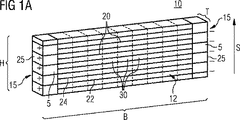
本発明による製造方法の第1実施例によれば、以下のステップを有している。すなわち、多層バーの積層方向で、複数の圧電セラミック層と複数の電極の交互に配置された構成からなる素地としての多層バーを形成し、それによって前記積層方向に対して垂直方向の多層バーの奥行きは1つの多層アクチュエータの奥行きに相応させ、前記積層方向に対して垂直方向の多層バーの幅は複数の多層アクチュエータの幅に相応させ、さらに前記複数の電極は前記多層バーの奥行き全体に亘って延在させ、さらに前記複数の電極は、前記多層バーの対向する端面において始めから交互に若しくは1つおきに多層バーの幅全体には延在しないようにさせるステップと、対向する補助電極を、多層バーの幅だけ離間された前記端面に配設し、それによって積層方向で電極1つ分ずらされている対向する補助電極を用いて、それぞれ1つおきの電極を駆動制御可能にするステップと、前記多層バーの奥行きに平行な方向で、1つおきの電極の側面に電気化学的なセットバック、特にエッチングを施し、それによって前記多層バーの対向する広幅側においてそれぞれ1つおきの電極が当該多層バー内へセットバックされ、さらにこのセットバックされた電極側面が積層方向で多層バーの対向する広幅側にて圧電層1つ分だけ互いに離間されるステップと、前記電極のセットバックされた側面に電気的な絶縁層をコーティングし、積層方向に対して平行な方向で多層バーの対向する広幅側にそれぞれ複数の外部電極を被着させるステップと、当該多層バーの奥行きに平行な方向と積層方向で前記多層バーを焼結し複数の圧電セラミック多層アクチュエータに分離させるステップとを有している。
Claims (3)
- 圧電セラミック多層アクチュエータを製造するための方法において、
a)多層バー(10)の積層方向(S)で、複数の圧電セラミック層(30)と複数の電極(20)の交互配置された構成からなる素地としての多層バー(10)を形成し、その際には前記多層バー(10)の積層方向(S)に垂直な方向での奥行き(T)は1つの多層アクチュエータの奥行きに相応させ、前記多層バー(10)の積層方向(S)に垂直な方向での幅(B)は複数の多層アクチュエータの幅に相応させ、さらに前記複数の電極(20)は前記多層バー(10)の全奥行き(T)に亘って延在させ、さらに前記複数の電極(20)は、前記多層バー(10)の対向する端面(15)において開始部分から交互に若しくは1つおきに多層バー(10)の幅(B)全体には延在しないように構成するステップと、
b)対向する補助電極(25)を、多層バー(10)の幅(B)だけ離間された前記端面(15)に配設し、それによって積層方向(S)で電極(20)1つ分ずらされている対向する補助電極(25)を用いて、それぞれ1つおきの電極(20)を電気的に駆動制御可能にするステップと、
c)前記多層バー(10)の奥行き(T)方向に平行な方向で、1つおきの電極(20)の側面(22;24)に電気化学的なセットバック、特にエッチングを施し、それによって前記多層バー(10)の対向する広幅側(12)においてそれぞれ1つおきの電極(20)の側面(22;24)が当該多層バー(10)内へセットバックされ、このセットバックされた電極(20)側面(22;24)が多層バー(10)の対向する広幅側(12)において積層方向(S)で圧電層(30)1つ分だけ相互に離間されるステップと、
d)前記セットバックされた電極(20)の側面(22;24)に電気的な絶縁層をコーティングし、前記多層バー(10)の対向する広幅側(12)において積層方向(S)に対して平行な方向でそれぞれ複数の外部電極を被着させるステップと、
e)当該多層バー(10)の奥行き(T)方向に平行な方向、積層方向(S)で前記多層バー(10)を焼結し複数の圧電セラミック多層アクチュエータに分離させるステップとを有し、
前記セットバックされた電極(20)側面(22;24)がそれぞれ凹部(40)内に設けられ、該凹部(40)はセラミック若しくはガラス状のスリップキャスティングからなる電気的な絶縁層によるコーティングのために充填され焼成されるようにしたことを特徴とする製造方法。 - 前記複数の外部電極は、多層バー(10)の対向する広幅側(12)に印刷される、請求項1記載の製造方法。
- 前記補助電極(25)を備えた端面(15)は、圧電的に不活性な領域(5)が多層バー(10)内に何も残らないように分離される、請求項1または2記載の製造方法。
Applications Claiming Priority (3)
| Application Number | Priority Date | Filing Date | Title |
|---|---|---|---|
| DE102007004813.2 | 2007-01-31 | ||
| DE102007004813.2A DE102007004813B4 (de) | 2007-01-31 | 2007-01-31 | Verfahren zur Herstellung eines piezokeramischen Vielschichtaktors |
| PCT/EP2008/050403 WO2008092740A2 (de) | 2007-01-31 | 2008-01-15 | Piezokeramischer vielschichtaktor und verfahren zu seiner herstellung |
Publications (3)
| Publication Number | Publication Date |
|---|---|
| JP2010517311A JP2010517311A (ja) | 2010-05-20 |
| JP2010517311A5 JP2010517311A5 (ja) | 2012-09-20 |
| JP5167280B2 true JP5167280B2 (ja) | 2013-03-21 |
Family
ID=39201439
Family Applications (1)
| Application Number | Title | Priority Date | Filing Date |
|---|---|---|---|
| JP2009547627A Active JP5167280B2 (ja) | 2007-01-31 | 2008-01-15 | 圧電セラミック多層アクチュエータ及びその製造方法 |
Country Status (7)
| Country | Link |
|---|---|
| US (1) | US7905000B2 (ja) |
| EP (1) | EP2126995B1 (ja) |
| JP (1) | JP5167280B2 (ja) |
| CN (1) | CN101601147B (ja) |
| AT (1) | ATE540434T1 (ja) |
| DE (1) | DE102007004813B4 (ja) |
| WO (1) | WO2008092740A2 (ja) |
Families Citing this family (18)
| Publication number | Priority date | Publication date | Assignee | Title |
|---|---|---|---|---|
| DE102009028259A1 (de) * | 2009-08-05 | 2011-02-10 | Robert Bosch Gmbh | Verfahren zur Herstellung von piezoelektrischen Werkstücken |
| DE102010022911B4 (de) * | 2010-06-07 | 2017-01-19 | Continental Automotive Gmbh | Verfahren zum Herstellen eines Piezoaktors und Piezoaktor |
| DE102010044739A1 (de) * | 2010-09-08 | 2012-03-08 | Epcos Ag | Verfahren zum Herstellen von piezoelektrischen Aktoren aus einem Materialblock |
| DE102012101351A1 (de) | 2012-02-20 | 2013-08-22 | Epcos Ag | Vielschichtbauelement und Verfahren zum Herstellen eines Vielschichtbauelements |
| WO2013124267A1 (de) | 2012-02-24 | 2013-08-29 | Epcos Ag | Verfahren zur herstellung einer elektrischen kontaktierung eines vielschichtbauelements und vielschichtbauelement mit einer elektrischen kontaktierung |
| DE102012207598A1 (de) * | 2012-05-08 | 2013-11-14 | Continental Automotive Gmbh | Verfahren zum elektrischen Kontaktieren eines elektronischen Bauelements als Stapel und elektronisches Bauelement mit einer Kontaktierungsstruktur |
| DE102012104830A1 (de) * | 2012-06-04 | 2013-12-05 | Epcos Ag | Vielschichtbauelement und Verfahren zum Herstellen eines Vielschichtbauelements |
| DE102012105059A1 (de) | 2012-06-12 | 2013-12-12 | Epcos Ag | Verfahren zur Herstellung eines Vielschichtbauelements und Vielschichtbauelement |
| DE102012105287B4 (de) | 2012-06-18 | 2020-07-02 | Tdk Electronics Ag | Verfahren zur Herstellung eines elektrischen Bauelements und Elektrisches Bauelement |
| DE102012107341B4 (de) | 2012-08-09 | 2020-07-09 | Tdk Electronics Ag | Verfahren zum Befüllen von mindestens einer Kavität eines Vielschichtbauelements mit einem Füllmaterial |
| DE102013111121B4 (de) | 2013-08-27 | 2020-03-26 | Tdk Electronics Ag | Verfahren zur Herstellung von keramischen Vielschichtbauelementen |
| DE102013017350B4 (de) | 2013-10-17 | 2020-07-09 | Tdk Electronics Ag | Vielschichtbauelement und Verfahren zur Herstellung eines Vielschichtbauelements |
| DE102015214778A1 (de) * | 2015-08-03 | 2017-02-09 | Continental Automotive Gmbh | Herstellungsverfahren zum Herstellen eines elektromechanischen Aktors und elektromechanischer Aktor |
| DE102015217334B3 (de) | 2015-09-10 | 2016-12-01 | Continental Automotive Gmbh | Verfahren zum Herstellen eines als Stapel ausgebildeten Vielschichtaktors |
| DE102015218701A1 (de) * | 2015-09-29 | 2016-12-01 | Continental Automotive Gmbh | Elektrokeramisches Bauelement, insbesondere Vielschichtpiezoaktor |
| US11437560B2 (en) * | 2017-06-22 | 2022-09-06 | Taiyo Yuden Co., Ltd. | Multilayer piezoelectric element, piezoelectric vibration apparatus, and electronic device |
| CN109994597A (zh) * | 2017-12-29 | 2019-07-09 | 苏州攀特电陶科技股份有限公司 | 多层压电陶瓷执行器及其制备方法 |
| EP3654355A1 (de) * | 2018-11-14 | 2020-05-20 | Siemens Aktiengesellschaft | Elektroblech mit strukturierter oberfläche zur domänenverfeinerung |
Family Cites Families (24)
| Publication number | Priority date | Publication date | Assignee | Title |
|---|---|---|---|---|
| JPH01184968A (ja) * | 1988-01-20 | 1989-07-24 | Hitachi Chem Co Ltd | 積層型圧電素子の製造法 |
| US4988909A (en) * | 1989-01-20 | 1991-01-29 | Mitsui Toatsu Chemicals, Inc. | Piezoelectric element with giant electrostrictive effect and ceramic composition for preparing same |
| US5191688A (en) * | 1989-07-27 | 1993-03-09 | Olympus Optical Co., Ltd. | Method for producing a superior longitudinal vibrator |
| WO1992005593A1 (en) * | 1990-09-13 | 1992-04-02 | Hitachi Metals, Ltd. | Method for manufacturing electrostrictive effect element |
| JPH04340778A (ja) * | 1991-01-30 | 1992-11-27 | Nec Corp | 積層圧電アクチュエータ素子 |
| JPH0529680A (ja) | 1991-07-25 | 1993-02-05 | Hitachi Metals Ltd | 積層型変位素子およびその製造方法 |
| JPH05267743A (ja) * | 1992-03-23 | 1993-10-15 | Sumitomo Metal Ind Ltd | 積層型圧電アクチュエータの製造方法 |
| JP3149611B2 (ja) * | 1993-03-26 | 2001-03-26 | 株式会社村田製作所 | 積層セラミック電子部品の製造方法 |
| JP2830724B2 (ja) | 1993-12-20 | 1998-12-02 | 日本電気株式会社 | 圧電アクチュエータの製造方法 |
| US5680685A (en) * | 1995-06-07 | 1997-10-28 | Microelectronic Packaging, Inc. | Method of fabricating a multilayer ceramic capacitor |
| DE19615695C1 (de) * | 1996-04-19 | 1997-07-03 | Siemens Ag | Verfahren zur Herstellung eines Piezoaktors monolithischer Vielschichtbauweise |
| DE19936713C2 (de) * | 1999-08-06 | 2001-08-23 | Bosch Gmbh Robert | Piezokeramischer Aktor sowie Verfahren zu seiner Herstellung |
| JP3397753B2 (ja) * | 1999-09-30 | 2003-04-21 | ティーディーケイ株式会社 | 積層型圧電素子およびその製造方法 |
| DE10021919C2 (de) * | 2000-02-04 | 2002-03-07 | Pi Ceramic Gmbh | Verfahren zur Herstellung monolithischer piezokeramischer Vielschichtaktoren sowie monolithischer piezokeramischer Vielschichtaktor |
| DE10205928A1 (de) * | 2001-02-21 | 2002-08-22 | Ceramtec Ag | Verfahren zur Herstellung piezokeramischer Vielschichtaktoren |
| CN2480846Y (zh) * | 2001-06-22 | 2002-03-06 | 中国科学院上海硅酸盐研究所 | 一种具有圆环状压电陶瓷多层膜结构的加速度传感器 |
| JP2003109839A (ja) * | 2001-10-01 | 2003-04-11 | Murata Mfg Co Ltd | 積層型電子部品の製造方法 |
| JP2004297041A (ja) * | 2003-03-12 | 2004-10-21 | Denso Corp | 積層型圧電体素子 |
| US7633210B2 (en) * | 2003-07-28 | 2009-12-15 | Kyocera Corporation | Multi-layer electronic component and method for manufacturing the same, multi-layer piezoelectric element |
| JP4470504B2 (ja) * | 2004-02-03 | 2010-06-02 | 株式会社デンソー | 積層型圧電素子及びその製造方法 |
| WO2005075113A1 (de) | 2004-02-06 | 2005-08-18 | Siemens Aktiengesellschaft | Ultraschallwandler mit einem piezoelektrischen wandlerelement, verfahren zum herstellen des wandlerelements und verwendung des ultraschallwandlers |
| DE102005008363B4 (de) * | 2005-02-23 | 2007-03-22 | Siemens Ag | Antriebseinheit mit einem eingebauten piezoelektrischen Stapelaktor mit verbesserter Wärmeableitung |
| DE102006001656A1 (de) * | 2005-07-26 | 2007-02-08 | Siemens Ag | Piezoaktor und Verfahren zur Herstellung desselben |
| US20070182288A1 (en) * | 2006-02-07 | 2007-08-09 | Fujifilm Corporation | Multilayered piezoelectric element and method of manufacturing the same |
-
2007
- 2007-01-31 DE DE102007004813.2A patent/DE102007004813B4/de active Active
-
2008
- 2008-01-15 EP EP08707901A patent/EP2126995B1/de active Active
- 2008-01-15 AT AT08707901T patent/ATE540434T1/de active
- 2008-01-15 JP JP2009547627A patent/JP5167280B2/ja active Active
- 2008-01-15 CN CN200880003824.7A patent/CN101601147B/zh not_active Expired - Fee Related
- 2008-01-15 US US12/524,549 patent/US7905000B2/en not_active Expired - Fee Related
- 2008-01-15 WO PCT/EP2008/050403 patent/WO2008092740A2/de active Application Filing
Also Published As
| Publication number | Publication date |
|---|---|
| CN101601147B (zh) | 2011-08-03 |
| EP2126995B1 (de) | 2012-01-04 |
| EP2126995A2 (de) | 2009-12-02 |
| WO2008092740A3 (de) | 2008-09-18 |
| US20090320255A1 (en) | 2009-12-31 |
| US7905000B2 (en) | 2011-03-15 |
| ATE540434T1 (de) | 2012-01-15 |
| CN101601147A (zh) | 2009-12-09 |
| DE102007004813B4 (de) | 2016-01-14 |
| JP2010517311A (ja) | 2010-05-20 |
| WO2008092740A2 (de) | 2008-08-07 |
| DE102007004813A1 (de) | 2008-08-14 |
Similar Documents
| Publication | Publication Date | Title |
|---|---|---|
| JP5167280B2 (ja) | 圧電セラミック多層アクチュエータ及びその製造方法 | |
| JP2010517311A5 (ja) | ||
| JP4440349B2 (ja) | 圧電式アクチュエータの製造方法および圧電式アクチュエータ | |
| US5254212A (en) | Method of fabricating electrostrictive-effect device | |
| WO2007031700A1 (en) | Piezoelectric actuator | |
| JP2017079333A (ja) | 多層デバイスの製造方法および多層デバイス | |
| JP2830724B2 (ja) | 圧電アクチュエータの製造方法 | |
| US8132304B2 (en) | Method of manufacturing a piezoelectric actuator | |
| US10608163B2 (en) | Multilayer component having internal electrodes alternatingly connected to external electrodes | |
| US5735027A (en) | Method of manufacturing a multilayer ceramic electronic component | |
| JP2004048015A (ja) | 圧電多層アクチュエータの製造方法及び該方法により製造されたアクチュエータ | |
| JP5666799B2 (ja) | セラミックコンデンサ及びその製造方法 | |
| JP5739611B2 (ja) | セラミックコンデンサ及びその製造方法 | |
| JP6306698B2 (ja) | 多層デバイスおよび多層デバイスを製造するための方法 | |
| JPH06151999A (ja) | 積層型圧電/電歪アクチュエータ素子の製造方法 | |
| JP6082002B2 (ja) | 積層型圧電素子 | |
| JPS60128683A (ja) | 積層型圧電アクチユエ−タの製造方法 | |
| JPH04170016A (ja) | 積層セラミック電子部品の製造方法 | |
| JP6035773B2 (ja) | 積層型圧電アクチュエータおよびその製造方法 | |
| JP2007266468A (ja) | 積層型圧電素子 | |
| JP2003258332A (ja) | セラミック積層体の製造方法 | |
| JP3846004B2 (ja) | ゲル状物質を用いる膜の製造方法、pzt膜の製造方法およびpzt膜 | |
| JP2003174209A (ja) | 積層型圧電アクチュエータ素子 | |
| JP2004079825A (ja) | 積層型圧電セラミックス素子およびその製造方法 | |
| JP2009252829A (ja) | 積層型圧電アクチュエータの製造方法 |
Legal Events
| Date | Code | Title | Description |
|---|---|---|---|
| RD04 | Notification of resignation of power of attorney |
Free format text: JAPANESE INTERMEDIATE CODE: A7424 Effective date: 20101228 |
|
| A977 | Report on retrieval |
Free format text: JAPANESE INTERMEDIATE CODE: A971007 Effective date: 20120425 |
|
| A131 | Notification of reasons for refusal |
Free format text: JAPANESE INTERMEDIATE CODE: A131 Effective date: 20120502 |
|
| A524 | Written submission of copy of amendment under article 19 pct |
Free format text: JAPANESE INTERMEDIATE CODE: A524 Effective date: 20120731 |
|
| TRDD | Decision of grant or rejection written | ||
| A01 | Written decision to grant a patent or to grant a registration (utility model) |
Free format text: JAPANESE INTERMEDIATE CODE: A01 Effective date: 20121122 |
|
| A61 | First payment of annual fees (during grant procedure) |
Free format text: JAPANESE INTERMEDIATE CODE: A61 Effective date: 20121221 |
|
| FPAY | Renewal fee payment (event date is renewal date of database) |
Free format text: PAYMENT UNTIL: 20151228 Year of fee payment: 3 |
|
| R150 | Certificate of patent or registration of utility model |
Free format text: JAPANESE INTERMEDIATE CODE: R150 Ref document number: 5167280 Country of ref document: JP Free format text: JAPANESE INTERMEDIATE CODE: R150 |
|
| R250 | Receipt of annual fees |
Free format text: JAPANESE INTERMEDIATE CODE: R250 |
|
| S111 | Request for change of ownership or part of ownership |
Free format text: JAPANESE INTERMEDIATE CODE: R313113 |
|
| R350 | Written notification of registration of transfer |
Free format text: JAPANESE INTERMEDIATE CODE: R350 |
|
| R250 | Receipt of annual fees |
Free format text: JAPANESE INTERMEDIATE CODE: R250 |
|
| R250 | Receipt of annual fees |
Free format text: JAPANESE INTERMEDIATE CODE: R250 |
|
| R250 | Receipt of annual fees |
Free format text: JAPANESE INTERMEDIATE CODE: R250 |
|
| R250 | Receipt of annual fees |
Free format text: JAPANESE INTERMEDIATE CODE: R250 |
|
| R250 | Receipt of annual fees |
Free format text: JAPANESE INTERMEDIATE CODE: R250 |
|
| R250 | Receipt of annual fees |
Free format text: JAPANESE INTERMEDIATE CODE: R250 |
|
| R250 | Receipt of annual fees |
Free format text: JAPANESE INTERMEDIATE CODE: R250 |
|
| S111 | Request for change of ownership or part of ownership |
Free format text: JAPANESE INTERMEDIATE CODE: R313113 |
|
| R360 | Written notification for declining of transfer of rights |
Free format text: JAPANESE INTERMEDIATE CODE: R360 |
|
| R360 | Written notification for declining of transfer of rights |
Free format text: JAPANESE INTERMEDIATE CODE: R360 |
|
| R371 | Transfer withdrawn |
Free format text: JAPANESE INTERMEDIATE CODE: R371 |
|
| S111 | Request for change of ownership or part of ownership |
Free format text: JAPANESE INTERMEDIATE CODE: R313113 |
|
| R350 | Written notification of registration of transfer |
Free format text: JAPANESE INTERMEDIATE CODE: R350 |
|
| R250 | Receipt of annual fees |
Free format text: JAPANESE INTERMEDIATE CODE: R250 |