JP5167280B2 - Piezoelectric ceramic multilayer actuator and manufacturing method thereof - Google Patents
Piezoelectric ceramic multilayer actuator and manufacturing method thereof Download PDFInfo
- Publication number
- JP5167280B2 JP5167280B2 JP2009547627A JP2009547627A JP5167280B2 JP 5167280 B2 JP5167280 B2 JP 5167280B2 JP 2009547627 A JP2009547627 A JP 2009547627A JP 2009547627 A JP2009547627 A JP 2009547627A JP 5167280 B2 JP5167280 B2 JP 5167280B2
- Authority
- JP
- Japan
- Prior art keywords
- multilayer
- bar
- electrode
- multilayer bar
- electrodes
- Prior art date
- Legal status (The legal status is an assumption and is not a legal conclusion. Google has not performed a legal analysis and makes no representation as to the accuracy of the status listed.)
- Active
Links
- 238000004519 manufacturing process Methods 0.000 title claims abstract description 31
- 239000000919 ceramic Substances 0.000 title claims description 33
- 238000000034 method Methods 0.000 claims abstract description 33
- 238000007569 slipcasting Methods 0.000 claims abstract description 8
- 238000005245 sintering Methods 0.000 claims description 13
- 238000005530 etching Methods 0.000 claims description 10
- 239000000758 substrate Substances 0.000 claims description 4
- 239000011248 coating agent Substances 0.000 claims description 3
- 238000000576 coating method Methods 0.000 claims description 3
- 238000000151 deposition Methods 0.000 claims description 2
- 238000001465 metallisation Methods 0.000 abstract description 10
- 230000008569 process Effects 0.000 description 19
- 239000004020 conductor Substances 0.000 description 8
- 239000000463 material Substances 0.000 description 7
- 238000010438 heat treatment Methods 0.000 description 6
- 238000009713 electroplating Methods 0.000 description 5
- 238000011282 treatment Methods 0.000 description 5
- 230000015572 biosynthetic process Effects 0.000 description 3
- 230000005684 electric field Effects 0.000 description 3
- 238000004070 electrodeposition Methods 0.000 description 3
- 239000003792 electrolyte Substances 0.000 description 3
- 238000010030 laminating Methods 0.000 description 3
- 238000005498 polishing Methods 0.000 description 3
- 229910001252 Pd alloy Inorganic materials 0.000 description 2
- FAPWRFPIFSIZLT-UHFFFAOYSA-M Sodium chloride Chemical compound [Na+].[Cl-] FAPWRFPIFSIZLT-UHFFFAOYSA-M 0.000 description 2
- 230000000694 effects Effects 0.000 description 2
- 239000007772 electrode material Substances 0.000 description 2
- 230000003628 erosive effect Effects 0.000 description 2
- 238000010304 firing Methods 0.000 description 2
- 238000009413 insulation Methods 0.000 description 2
- SWELZOZIOHGSPA-UHFFFAOYSA-N palladium silver Chemical compound [Pd].[Ag] SWELZOZIOHGSPA-UHFFFAOYSA-N 0.000 description 2
- 239000000843 powder Substances 0.000 description 2
- 238000003825 pressing Methods 0.000 description 2
- 238000000926 separation method Methods 0.000 description 2
- VWDWKYIASSYTQR-UHFFFAOYSA-N sodium nitrate Chemical compound [Na+].[O-][N+]([O-])=O VWDWKYIASSYTQR-UHFFFAOYSA-N 0.000 description 2
- 230000007704 transition Effects 0.000 description 2
- 240000006829 Ficus sundaica Species 0.000 description 1
- 230000009471 action Effects 0.000 description 1
- 239000000956 alloy Substances 0.000 description 1
- 229910045601 alloy Inorganic materials 0.000 description 1
- 230000008602 contraction Effects 0.000 description 1
- 238000007796 conventional method Methods 0.000 description 1
- 239000013078 crystal Substances 0.000 description 1
- 238000005520 cutting process Methods 0.000 description 1
- 238000005137 deposition process Methods 0.000 description 1
- 238000010586 diagram Methods 0.000 description 1
- 238000010292 electrical insulation Methods 0.000 description 1
- 239000012777 electrically insulating material Substances 0.000 description 1
- 239000011521 glass Substances 0.000 description 1
- PCHJSUWPFVWCPO-UHFFFAOYSA-N gold Chemical compound [Au] PCHJSUWPFVWCPO-UHFFFAOYSA-N 0.000 description 1
- 239000010931 gold Substances 0.000 description 1
- 229910052737 gold Inorganic materials 0.000 description 1
- 230000033444 hydroxylation Effects 0.000 description 1
- 238000005805 hydroxylation reaction Methods 0.000 description 1
- 239000011810 insulating material Substances 0.000 description 1
- 238000003475 lamination Methods 0.000 description 1
- 238000013532 laser treatment Methods 0.000 description 1
- 229910021645 metal ion Inorganic materials 0.000 description 1
- 238000000465 moulding Methods 0.000 description 1
- 238000005457 optimization Methods 0.000 description 1
- 238000007639 printing Methods 0.000 description 1
- 238000003672 processing method Methods 0.000 description 1
- 230000002250 progressing effect Effects 0.000 description 1
- 230000009467 reduction Effects 0.000 description 1
- 238000007650 screen-printing Methods 0.000 description 1
- 239000011780 sodium chloride Substances 0.000 description 1
- 235000010344 sodium nitrate Nutrition 0.000 description 1
- 239000004317 sodium nitrate Substances 0.000 description 1
- 239000000126 substance Substances 0.000 description 1
Images


Classifications
-
- H—ELECTRICITY
- H10—SEMICONDUCTOR DEVICES; ELECTRIC SOLID-STATE DEVICES NOT OTHERWISE PROVIDED FOR
- H10N—ELECTRIC SOLID-STATE DEVICES NOT OTHERWISE PROVIDED FOR
- H10N30/00—Piezoelectric or electrostrictive devices
- H10N30/01—Manufacture or treatment
- H10N30/06—Forming electrodes or interconnections, e.g. leads or terminals
- H10N30/063—Forming interconnections, e.g. connection electrodes of multilayered piezoelectric or electrostrictive parts
-
- H—ELECTRICITY
- H10—SEMICONDUCTOR DEVICES; ELECTRIC SOLID-STATE DEVICES NOT OTHERWISE PROVIDED FOR
- H10N—ELECTRIC SOLID-STATE DEVICES NOT OTHERWISE PROVIDED FOR
- H10N30/00—Piezoelectric or electrostrictive devices
- H10N30/01—Manufacture or treatment
- H10N30/05—Manufacture of multilayered piezoelectric or electrostrictive devices, or parts thereof, e.g. by stacking piezoelectric bodies and electrodes
- H10N30/053—Manufacture of multilayered piezoelectric or electrostrictive devices, or parts thereof, e.g. by stacking piezoelectric bodies and electrodes by integrally sintering piezoelectric or electrostrictive bodies and electrodes
-
- Y—GENERAL TAGGING OF NEW TECHNOLOGICAL DEVELOPMENTS; GENERAL TAGGING OF CROSS-SECTIONAL TECHNOLOGIES SPANNING OVER SEVERAL SECTIONS OF THE IPC; TECHNICAL SUBJECTS COVERED BY FORMER USPC CROSS-REFERENCE ART COLLECTIONS [XRACs] AND DIGESTS
- Y10—TECHNICAL SUBJECTS COVERED BY FORMER USPC
- Y10T—TECHNICAL SUBJECTS COVERED BY FORMER US CLASSIFICATION
- Y10T29/00—Metal working
- Y10T29/42—Piezoelectric device making
-
- Y—GENERAL TAGGING OF NEW TECHNOLOGICAL DEVELOPMENTS; GENERAL TAGGING OF CROSS-SECTIONAL TECHNOLOGIES SPANNING OVER SEVERAL SECTIONS OF THE IPC; TECHNICAL SUBJECTS COVERED BY FORMER USPC CROSS-REFERENCE ART COLLECTIONS [XRACs] AND DIGESTS
- Y10—TECHNICAL SUBJECTS COVERED BY FORMER USPC
- Y10T—TECHNICAL SUBJECTS COVERED BY FORMER US CLASSIFICATION
- Y10T29/00—Metal working
- Y10T29/49—Method of mechanical manufacture
- Y10T29/49002—Electrical device making
- Y10T29/49117—Conductor or circuit manufacturing
- Y10T29/49124—On flat or curved insulated base, e.g., printed circuit, etc.
- Y10T29/49126—Assembling bases
-
- Y—GENERAL TAGGING OF NEW TECHNOLOGICAL DEVELOPMENTS; GENERAL TAGGING OF CROSS-SECTIONAL TECHNOLOGIES SPANNING OVER SEVERAL SECTIONS OF THE IPC; TECHNICAL SUBJECTS COVERED BY FORMER USPC CROSS-REFERENCE ART COLLECTIONS [XRACs] AND DIGESTS
- Y10—TECHNICAL SUBJECTS COVERED BY FORMER USPC
- Y10T—TECHNICAL SUBJECTS COVERED BY FORMER US CLASSIFICATION
- Y10T29/00—Metal working
- Y10T29/49—Method of mechanical manufacture
- Y10T29/49002—Electrical device making
- Y10T29/49117—Conductor or circuit manufacturing
- Y10T29/49124—On flat or curved insulated base, e.g., printed circuit, etc.
- Y10T29/49128—Assembling formed circuit to base
-
- Y—GENERAL TAGGING OF NEW TECHNOLOGICAL DEVELOPMENTS; GENERAL TAGGING OF CROSS-SECTIONAL TECHNOLOGIES SPANNING OVER SEVERAL SECTIONS OF THE IPC; TECHNICAL SUBJECTS COVERED BY FORMER USPC CROSS-REFERENCE ART COLLECTIONS [XRACs] AND DIGESTS
- Y10—TECHNICAL SUBJECTS COVERED BY FORMER USPC
- Y10T—TECHNICAL SUBJECTS COVERED BY FORMER US CLASSIFICATION
- Y10T29/00—Metal working
- Y10T29/49—Method of mechanical manufacture
- Y10T29/49002—Electrical device making
- Y10T29/49117—Conductor or circuit manufacturing
- Y10T29/49124—On flat or curved insulated base, e.g., printed circuit, etc.
- Y10T29/49155—Manufacturing circuit on or in base
- Y10T29/49163—Manufacturing circuit on or in base with sintering of base
Abstract
Description
本発明は、圧電セラミック多層アクチュエータ及びその製造方法に関している。 The present invention relates to a piezoelectric ceramic multilayer actuator and a manufacturing method thereof.
圧電セラミッスに適した結晶構造では、電界形成の際の圧電効果に基づいて、その内部に膨張又は収縮が生じ得る。このような長さ変化はほぼ、制御される電気信号に関する遅延なしで発生し、さらに正確に制御可能である。それ故に圧電多層アクチュエータは制御素子として用いられている。 In a crystal structure suitable for piezoelectric ceramics, expansion or contraction may occur in the inside thereof based on the piezoelectric effect during electric field formation. Such length changes occur almost without delay with respect to the controlled electrical signal and can be controlled more precisely. Therefore, piezoelectric multilayer actuators are used as control elements.
しかしながらそのような多層アクチュエータにおいて制御すべき電界は数kV/mmの範囲にあるので、多層アクチュエータの実際の使用においては中程度のほどよい駆動制御電圧が望まれている。そのため圧電セラミック多層アクチュエータは100μmの範囲の層厚さで製造される。典型的な製造方法にはスリップキャスティング手法(slip casting)やドライプレス(dry pressing)手法がある。個々のセラミック層は金属化され、上下に積層される。それにより2つのセラミック層の間に設けられた逆極性の内部電極が圧電効果を生ぜしめる。圧電セラミック多層アクチュエータの積層方向ないしは長手軸に対して平行な外部金属化層を介して全ての内部電極が同じ電位の全ての内部電極が電気的に駆動される。それぞれ逆電位の内部電極を短絡させないようにするためには、これらがそれぞれ逆電位の内部電極の外側金属化部の領域において、他の電極に対してずらして配置する必要がある。デザイン要素のために、圧電不活性領域が圧電セラミック多層アクチュエータ内部のこのような層構造によって生じる。圧電セラミック多層アクチュエータは圧電活性領域においてのみその長さが膨張若しくは収縮し、この領域内では異なる電位の内部電極が直接上下に配置されているので、圧電不活性領域への移行領域においては多層アクチュエータ内部で機械的緊張が発生する。この機械的な緊張は、多層アクチュエータの層構造においてクラック(ひび割れ)を形成する。このことは外側金属化部と個々の電極との電気的なコンタクトに影響を及ぼし、場合によっては当該多層アクチュエータ全体の故障につながりかねない。前述したクラック形成の問題は、フルアクティブな圧電多層アクチュエータの使用によって低減される。このようなフルアクティブな圧電多層アクチュエータにおいては、圧電不活性領域ないし不動態領域は存在しない。なぜなら両電位の内部電極が多層アクチュエータの全断面に亘って全ての側でその縁部まで延在しているからである。 However, since the electric field to be controlled in such a multilayer actuator is in the range of several kV / mm, a moderately good drive control voltage is desired in practical use of the multilayer actuator. Therefore, the piezoelectric ceramic multilayer actuator is manufactured with a layer thickness in the range of 100 μm. Typical manufacturing methods include slip casting and dry pressing. Individual ceramic layers are metallized and stacked one above the other. As a result, a reverse polarity internal electrode provided between the two ceramic layers produces a piezoelectric effect. All internal electrodes having the same potential are electrically driven through an external metallization layer parallel to the stacking direction or longitudinal axis of the piezoelectric ceramic multilayer actuator. In order not to short-circuit the internal electrodes having the opposite potentials, it is necessary to displace these from the other electrodes in the region of the outer metallized portion of the internal electrode having the reverse potential. Due to the design element, a piezoelectric inactive region is created by such a layer structure inside the piezoelectric ceramic multilayer actuator. Piezoelectric ceramic multilayer actuators expand or contract in length only in the piezoelectric active region, and internal electrodes of different potentials are directly arranged above and below in this region, so in the transition region to the piezoelectric inactive region, the multilayer actuator Mechanical tension is generated inside. This mechanical tension forms a crack in the layer structure of the multilayer actuator. This affects the electrical contact between the outer metallization and the individual electrodes, and in some cases can lead to failure of the entire multilayer actuator. The aforementioned crack formation problem is reduced by the use of a fully active piezoelectric multilayer actuator. In such a fully active piezoelectric multilayer actuator, there is no piezoelectric inactive region or passive region. This is because the internal electrodes of both potentials extend to the edge on all sides over the entire cross section of the multilayer actuator.
EP 1 206 804 B1明細書では、圧電多層アクチュエータのための製造方法が開示されている。ここでは個々多層構造部に同じ電位の電極の側面に導電性の材料が析出されている。この材料はブリッジを形成しており、このブリッジは当該ブリッジ間に配設される電極の側面の絶縁の後で互いに電気的に接続される。
In
DE 42 24 284 A1明細書には、圧電セラミック多層アクチュエータを製造する前段階としての多層バーの製造と、それに続くその焼結が開示されている。この種のバーは、後の多層アクチュエータに関するその積層方向に対して垂直方向の奥行きと水平方向での長さを有している。積層方向に対して垂直方向のその幅は、後の圧電セラミック多層アクチュエータの幅の数倍である。焼結後は個々の圧電セラミック多層アクチュエータの電極構造部が多層バーにおいて連帯的に形成され、それに続いて個々の多層アクチュエータへ分割される。電極構造部の製造に対してはそれぞれ第2電極の側面毎に導電性材料が析出される。この介在領域(すなわちセラミックと電極の)は、エッチングによって若しくは機械的な除去によって焼結多層バー内へセットバックされる。この過程は複雑で時間がかかる。なぜなら焼結される多層バーが機械的及び化学的作用に対する抵抗を有しているからである。それに続いてセットバックされた領域には絶縁層が被着され、後の多層アクチュエータ毎に外部電極が形成される。最終的に焼結された多層バーは個々の圧電セラミック多層アクチュエータに分割される。 DE 42 24 284 A1 discloses the production of a multilayer bar and the subsequent sintering thereof as a pre-stage for producing a piezoelectric ceramic multilayer actuator. This type of bar has a depth in the vertical direction and a length in the horizontal direction with respect to its stacking direction for the later multilayer actuator. Its width in the direction perpendicular to the stacking direction is several times the width of the subsequent piezoelectric ceramic multilayer actuator. After sintering, the electrode structures of the individual piezoceramic multilayer actuators are formed together in a multilayer bar and subsequently divided into individual multilayer actuators. For the manufacture of the electrode structure, a conductive material is deposited on each side surface of the second electrode. This intervening region (ie ceramic and electrode) is set back into the sintered multilayer bar by etching or by mechanical removal. This process is complex and time consuming. This is because the multilayer bar to be sintered has resistance to mechanical and chemical action. Subsequently, an insulating layer is deposited on the setback region, and an external electrode is formed for each subsequent multilayer actuator. The finally sintered multilayer bar is divided into individual piezoelectric ceramic multilayer actuators.
US 5,568,679明細書並びにWO 2005/075113 A1明細書にも、既に焼結された多層体において構造化される外部電極を形成する手法が記載されている。同じ電位の各内部電極には電気化学的に絶縁材料が析出されており、それによってこれらの電極の側面は外方に向けて絶縁される。それに続いて外側には、別の電位の電極のまだ露出している側面につながる導電性材料が被着される。最後に、構造化された電極を備えた焼結された多層バーが個々の圧電セラミック多層アクチュエータに分割される。 US 5,568,679 and WO 2005/075113 A1 also describe techniques for forming external electrodes that are structured in already sintered multilayer bodies. An insulating material is deposited electrochemically on each internal electrode at the same potential, whereby the sides of these electrodes are insulated outward. Subsequently, on the outside, a conductive material is deposited which leads to the still exposed side of another potential electrode. Finally, the sintered multilayer bar with structured electrodes is divided into individual piezoelectric ceramic multilayer actuators.
本発明の課題は、従来技法よりも少ない手間とコストで実施可能な、圧電セラミック多層アクチュエータの製造方法を提供することである。また本発明のさらなる課題は、相応に安価に製造できる圧電セラミック多層アクチュエータを提供することでもある。 An object of the present invention is to provide a method for manufacturing a piezoelectric ceramic multilayer actuator that can be implemented with less labor and cost than conventional techniques. A further object of the present invention is to provide a piezoelectric ceramic multilayer actuator that can be manufactured at a reasonable cost.
前記課題は、独立請求項に記載の本発明による方法、並びに独立請求項に記載の本発明による圧電セラミック多層アクチュエータによって解決される。本発明の有利な構成例及び改善例は以下の明細書、図面並びに特許請求の範囲に記載される。 The object is solved by the method according to the invention as defined in the independent claim and the piezoceramic multilayer actuator according to the invention as defined in the independent claim. Advantageous configurations and improvements of the present invention are described in the following specification, drawings and claims.
発明を実施するための形態
本発明による製造方法の第1実施例によれば、以下のステップを有している。すなわち、多層バーの積層方向で、複数の圧電セラミック層と複数の電極の交互に配置された構成からなる素地としての多層バーを形成し、それによって前記積層方向に対して垂直方向の多層バーの奥行きは1つの多層アクチュエータの奥行きに相応させ、前記積層方向に対して垂直方向の多層バーの幅は複数の多層アクチュエータの幅に相応させ、さらに前記複数の電極は前記多層バーの奥行き全体に亘って延在させ、さらに前記複数の電極は、前記多層バーの対向する端面において始めから交互に若しくは1つおきに多層バーの幅全体には延在しないようにさせるステップと、対向する補助電極を、多層バーの幅だけ離間された前記端面に配設し、それによって積層方向で電極1つ分ずらされている対向する補助電極を用いて、それぞれ1つおきの電極を駆動制御可能にするステップと、前記多層バーの奥行きに平行な方向で、1つおきの電極の側面に電気化学的なセットバック、特にエッチングを施し、それによって前記多層バーの対向する広幅側においてそれぞれ1つおきの電極が当該多層バー内へセットバックされ、さらにこのセットバックされた電極側面が積層方向で多層バーの対向する広幅側にて圧電層1つ分だけ互いに離間されるステップと、前記電極のセットバックされた側面に電気的な絶縁層をコーティングし、積層方向に対して平行な方向で多層バーの対向する広幅側にそれぞれ複数の外部電極を被着させるステップと、当該多層バーの奥行きに平行な方向と積層方向で前記多層バーを焼結し複数の圧電セラミック多層アクチュエータに分離させるステップとを有している。
BEST MODE FOR CARRYING OUT THE INVENTION The first embodiment of the manufacturing method according to the present invention includes the following steps. That is, in the stacking direction of the multi-layer bar, a multi-layer bar is formed as a substrate composed of a structure in which a plurality of piezoelectric ceramic layers and a plurality of electrodes are alternately arranged, thereby forming a multi-layer bar perpendicular to the stacking direction. The depth corresponds to the depth of one multilayer actuator, the width of the multilayer bar perpendicular to the stacking direction corresponds to the width of a plurality of multilayer actuators, and the plurality of electrodes extends over the entire depth of the multilayer bar. And extending the plurality of electrodes such that the plurality of electrodes do not extend across the entire width of the multilayer bar alternately or every other one from the beginning on the opposing end faces of the multilayer bar; , disposed on the end face spaced by the width of the multilayer bar, thereby using the auxiliary electrode facing is offset electrode one minute in the laminating direction, respectively A step of enabling the drive control every other electrode, in a direction parallel to the depth of the multilayer bar, electrochemical setback on the sides of every other electrode, in particular etched, whereby the multilayer bar On the opposite wide side, every other electrode is set back into the multilayer bar, and the side surfaces of the set back electrodes are separated from each other by one piezoelectric layer on the opposite wide side of the multilayer bar in the stacking direction. A step of coating an electrically insulating layer on the set-back side surface of the electrode and depositing a plurality of external electrodes on the opposite wide side of the multilayer bar in a direction parallel to the stacking direction. And sintering the multilayer bar in a direction parallel to the depth of the multilayer bar and a stacking direction to separate the multilayer bar into a plurality of piezoelectric ceramic multilayer actuators. The has.
フルアクティブな圧電セラミック多層アクチュエータの製造の手間とコストを低減するために、多層バーにおける製造ステップの大半がグリーンの状態、すなわち素地の状態で行われる。このバーは、また焼結されていないセラミック構造のために僅かな手間と僅かなコストで処理することが可能である。さらにこの補助電極を有する多層バーは、幅の分だけ離間したその端面において、複数の圧電セラミック多層アクチュエータを同時に製造することを可能にしている。その際には当該の多層バーが製造方法の最終段階において個々の多層アクチュエータに分離される。 In order to reduce the labor and cost of manufacturing a fully active piezoceramic multilayer actuator, most of the manufacturing steps in the multilayer bar are carried out in the green state, ie the green state. The bar can also be processed with little effort and cost due to the unsintered ceramic structure. Furthermore, the multi-layer bar having this auxiliary electrode makes it possible to simultaneously produce a plurality of piezoelectric ceramic multi-layer actuators at their end faces separated by a width. In that case, the multilayer bar is separated into individual multilayer actuators in the final stage of the production process.
多層バーの外側において構造化された電極を製造するために、まずそれぞれ第2の電極の側面がエッチングによって多層バー内へセットバックされるか場合によっては凹部が設けられる。そのように形成された凹み(この中にそれぞれ第2の電極の側面が配設される)は、焼成後に電気的に絶縁される材料のスリップキャスティングによって充填される。これらの材料は例えばガラスやセラミックである。エッチングやそれに続くスリップキャスティングによる電気的な絶縁に基づいて電気的に接続されるそれぞれ第2の電極の側面が凹部外側に露出されて配置され、それによって例えば外側金属化部の印刷の際に相互に電気的に接続されるようにしている。 In order to produce a structured electrode on the outside of the multilayer bar, first a side surface of the second electrode is first set back into the multilayer bar by etching or possibly a recess. The so-formed recesses (in which the side surfaces of the second electrode are respectively disposed) are filled by slip casting of a material that is electrically insulated after firing. These materials are, for example, glass and ceramic. The side surfaces of the respective second electrodes that are electrically connected based on electrical insulation by etching and subsequent slip casting are arranged so as to be exposed to the outside of the recesses, so that, for example, when printing the outer metallization part To be electrically connected.
本発明による別の製造方法によれば、前述した電気化学的セットバックの代わりに、1つおきの電極のそれぞれ1つの側面における導電性材料の電気化学的析出が行われ、それによって前記多層バーの対向する広幅側においてそれぞれ1つおきの電極側面が当該多層バーから突出し、該突出した電極側面は積層方向で多層バーの対向する広幅側にて圧電層1つ分だけ互いに離間し、当該の突出した電極側面の間で複数の凹部が形成される。 According to another manufacturing method according to the present invention, instead of the electrochemical setback described above, the electrochemical deposition of conductive material on each one side of every other electrode is performed, whereby the multilayer bar Every other electrode side surface protrudes from the multilayer bar on each of the opposing wide sides, and the protruding electrode side surfaces are separated from each other by one piezoelectric layer on the opposing wide side of the multilayer bar in the stacking direction. A plurality of recesses are formed between the protruding electrode side surfaces.
前述したような同様の方式でこの凹部は焼成後に電気的に絶縁性となる材料のスリップキャスティングによって充填される。そのため電気化学的析出によって高められた、多層バーの電極の側面のみがその広幅側において露出する。またこの方法過程のもとでは多層バーの簡単化された処理の利点並びにこれらの多層バーを用いた複数の多層アクチュエータの同時製造が用いられる。さらに有利には、凹部内に設けられる電気的に絶縁すべき電極の側面がスリップキャスティングによって効果的に絶縁可能である。そのうえさらにスリップキャスティングの焼成が多層バーの焼結と組合わせて行われる。これは当該製造方法のさらなる最適化を達成するためのものである。 In a similar manner as described above, this recess is filled by slip casting of a material that becomes electrically insulating after firing. Therefore, only the side surface of the multilayer bar electrode, which is enhanced by electrochemical deposition, is exposed on its wide side. Also, under this process, the advantages of simplified processing of the multilayer bars and the simultaneous production of a plurality of multilayer actuators using these multilayer bars are used. Further advantageously, the side surfaces of the electrode to be electrically insulated provided in the recess can be effectively insulated by slip casting. Moreover, slip casting is performed in combination with sintering of the multilayer bar. This is to achieve further optimization of the manufacturing method.
本発明による製造方法のさらに別の代替例によれば、以下の方法ステップが実施される。すなわち、多層バーの積層方向で、複数の圧電セラミック層と複数の電極の交互に配置された構成からなる素地としての多層バーを形成し、それによって前記積層方向に対して垂直方向の多層バーの奥行きは1つの多層アクチュエータの奥行きに相応させ、前記積層方向に対して垂直方向の多層バーの幅は複数の多層アクチュエータの幅に相応させ、さらに前記複数の電極は前記多層バーの全奥行きと幅に亘って延在させるか、または積層方向において複数の圧電セラミック層と複数の電極の交互に配置された構成からなる圧電的にフルアクティブなスタックを形成するステップと、前記多層バーの奥行き方向に平行する方向で1つおきの電極のそれぞれ1つの側面を、鋸引き処理、研磨処理、レーザー処理、浸食処理及び/又は成形処理によって除去し、それによって前記多層バーの対向する広幅側においてそれぞれ1つおきの電極が当該多層バー内へセットバックされ、さらにこのセットバックされた電極側面が積層方向で多層バーの対向する広幅側にて圧電層1つ分だけ互いに離間されるステップと、前記電極のセットバックされた側面に電気的な絶縁層をコーティングし、積層方向に対して平行な方向で多層バーの対向する広幅側にそれぞれ複数の外部電極を被着させるステップと、当該多層バーの奥行きに平行な方向と積層方向で前記多層バーを焼結し複数の圧電セラミック多層アクチュエータに分離させるステップが実施される。 According to yet another alternative of the production method according to the invention, the following method steps are carried out. That is, in the stacking direction of the multi-layer bar, a multi-layer bar is formed as a substrate composed of a structure in which a plurality of piezoelectric ceramic layers and a plurality of electrodes are alternately arranged, thereby forming a multi-layer bar perpendicular to the stacking direction. The depth corresponds to the depth of one multi-layer actuator, the width of the multi-layer bar perpendicular to the stacking direction corresponds to the width of a plurality of multi-layer actuators, and the plurality of electrodes have a total depth and width of the multi-layer bar. Forming a piezoelectrically fully active stack comprising a plurality of piezoelectric ceramic layers and a plurality of electrodes arranged alternately in the stacking direction, and in the depth direction of the multilayer bar each one side of every other electrode in a direction parallel sawing treatment, polishing treatment, laser treatment, the erosion processing and / or molding process It was removed I, whereby the multilayer bar opposite wide every each the side electrodes is set back to the multi-layer bar in further broad this set-back electrode side faces of a multilayer bar in the laminating direction A side separated from each other by one piezoelectric layer on the side, and an electrically insulating layer is coated on the set-back side surface of the electrode, and the wide side of the multilayer bar facing in the direction parallel to the stacking direction A plurality of external electrodes are attached to each other, and a step of sintering the multilayer bar in a direction parallel to the depth of the multilayer bar and a laminating direction and separating the multilayer bar into a plurality of piezoelectric ceramic multilayer actuators.
以下では本発明を図面に基づき詳細に説明する。 Hereinafter, the present invention will be described in detail with reference to the drawings.
圧電セラミック多層アクチュエータを製造するために、まず圧電セラミックのグリーンフィルム(素地)が注型される。それに続いてこのグリーンフィルムには電極材料が印刷される。この電極材料は例えば銀−パラジウム合金からなる。これらの面は後の内部電極20を形成する。さらに印刷されたそれらのグリーンフィルムは積層方向(スタック方向)Sで1つのスタックを形成すべく上下に積層される。有利には2つの印刷済みグリーンフィルムの間に未印刷のグリーンフィルムが配置される。これは後の多層アクチュエータ内部において電気的な短絡の危険性を低減させるためである。
To prepare the pressure conductive ceramic multilayer actuator, first piezoelectric ceramic green film (base material) is cast. Subsequently, an electrode material is printed on the green film. This electrode material is made of, for example, a silver-palladium alloy. These surfaces form a later
グリーンフィルムが積層処理された後ではこれらが1つのブロックとして存在する。このブロックの幅及び奥行きは、後の1つの多層アクチュエータの幅及び奥行きの数倍分に相応する。素地の状態ではこのブロックは化学的、機械的又はそれ以外の方式で処理するのに十分に安定している。さらにブロックの構造は、焼結された状態よりも抵抗が少なく、そのため少ないコストでブロックの処理が実施できる。 After the green film is laminated, these exist as one block. The width and depth of this block correspond to several times the width and depth of one subsequent multilayer actuator. In the green state, the block is sufficiently stable to be processed chemically, mechanically or otherwise. Furthermore, the structure of the block has less resistance than the sintered state, so that the block can be processed at a lower cost.
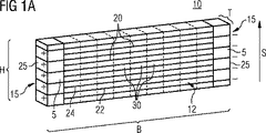
素地の状態のブロック(図示せず)は、例えば鋸引きによって複数の多層バー10に分割される。この多層バー10は素地体(グリーンボディ)として、積層方向Sで複数の圧電セラミック層30と複数の電極20の交互配置からなる構成を含んでいる。積層方向Sに対して垂直方向の多層バー10の奥行きTは、製造後の1つの多層アクチュエータの奥行きに相応し、積層方向Sに対して垂直な方向の多層バー10の幅Bは製造後の複数の多層アクチュエータの幅に相応している(図1A、B参照)。多層バー10の電極20は多層バー10の全奥行きTに亘って延在している。
The base block (not shown) is divided into a plurality of
1つの実施形態によれば(図1A参照)、多層バー10の高さHは、後の焼結された状態の多層アクチュエータの高さにほぼ相応している。さらなる処理ステップと焼結の後では(下方参照)、多層バー10が分離ステップによってその積層方向Sに平行な方向で個々の多層アクチュエータに分割される(図1A中の波線参照)。さらに別の実施形態によれば(図1B)、焼結処理された多層バー10が積層方向Sに対して平行及び垂直方向で切断によって波線に沿って分割される。素地状態における多層バー10を用いることによって、同時に多数の多層アクチュエータを製造することができる。それに対してはさらに製造方法の枠内で素地状態の容易な処理が有効利用される。
According to one embodiment (see FIG. 1A), the height H of the
素地状態の多層バー10は前述したような積層方向Sでそれぞれ交互に配置された圧電セラミック層30と電極20を含んでいる。電極20の側面22,24はそれぞれ多層バー10の広幅側12の表面まで届く。この多層バー10はその対向する端面側15にそれぞれ1つの補助電極25を含んでいる。1つおきの電極20は補助電極25のところから始まって対向する補助電極25の前で終端している。それ故に電極20は多層バー10の幅B全体に亘っては延在していない。側面22若しくは24を有する1つおきの電極20は、それによって補助電極25の使用に基づいて一緒に電気的駆動が可能である。このような構成から多層バー10の端面15に当接する圧電的に不活性な領域5も複数生じる。これらは多層アクチュエータの製造において失われた領域とみなされる。なぜならそれらは製造方法の終了後はさらなる使用には供されないからである。
The
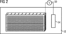
多層バー10を素地の状態で供給した後、すなわち、多層バーを製造するステップS1と補助電極を配設するステップS2の終了した後では、有利には広幅側12が不動体化層で絶縁される。不動体化層を被着した後は多層バー10が電解槽で電気化学的に処理を施される(図2参照)。ここでは不動体化層なしの多層バーを処理することも考えられる。そのようなケースでは多層バーの1つの広幅側12だけを電気化学的に処理すべく電解槽52に浸らせる(図2)。
After the supply of the
図2に示されている電気めっき槽を用いることによって多層バー10が電気化学的に処理され、そこでは電極20の側面22;24に導電材料がコーティングされる。この材料としては金、銀−パラジウム合金などや後の熱処理に耐えられるその他の材料、合金などが挙げられる。
The
電気めっき槽は電圧源50を介して電気めっき槽電極54と補助電極25の1つとの間で電気的な直流電圧を印加するために電解質52と電気メッキ槽電極54を含んでいる。直流電圧源50は補助電極25の1つにしか接続されていない。そのため広幅側12において側面22のみが電気的絶縁材料をコーティングされる。このコーティングの間は電解質52から金属イオンが電界中を電極方向20に遷移し、側面22において析出される。この析出過程の終了後は不動体化層が除去され、対向する広幅側12に被着されるか又は対向する広幅側12が電気メッキ槽に浸漬される。別の補助電極25が直流電圧源50と接続されることにより、対向する広幅側12においては電極20の側面24のみが導電材料をコーティングされる。
The electroplating bath includes an
それ故に対向する広幅側12においてコーティングされる側面22,24は、図3に示されているようにそれぞれ圧電層30の1つ分だけ相互に離間される。それと共に電極20の側面22または24における電気化学的に析出される導電材料は、凹部40も含んでおり、この凹部内にそれぞれ1つの電極20が配設されている。
Therefore, the side surfaces 22 and 24 that are coated on the opposite
さらに別の製造方法代替例によれば、図3に示されているものと類似の凹部構造が電界エッチングS4によって形成される。この目的のために多層バー10は広幅側12のみか若しくは事前に不動体化された広幅側12が完全にエッチング槽に浸漬される。このエッチング槽は有利には通常の電解液、例えば水酸化、塩化ナトリウム水溶液、硝酸ナトリウム水溶液などを含んでいる。その後で1つの補助電極25のみを介して電気的な直流電圧が電極20の側面22に印加される。それ故に電極20の側面22のみが電気化学的に除去される。その後で対向する広幅側12はエッチング槽に浸漬され、他の補助電極25が電気的に駆動される。それにより電極20の側面24が除去される。ここではまた対向する広幅側12に不動体化層を設け、別の補助電極25を電気的に駆動することも考えられる。このエッチング手法によれば、側面24がエッチング除去されるかないしはセットバックされる。それにより両方の広幅側12において電極20のそれぞれエッチングされない側面22ないし24の間に複数の凹部40が形成される。側面22,24は層30の圧電性の側面に比べて小さいので、それらは少ないコストでエッチングでき、それによって奥行きTの方向に平行な方向で多層バー10内部へセットバック(後退)される。
According to yet another manufacturing method alternative, a recess structure similar to that shown in FIG. 3 is formed by field etching S4. For this purpose, the
先行する製造ステップに依存することなく広幅側12で1つおきの電極20を電気的に絶縁するために(これによって外部金属化層が印刷され得るようになる(図11のステップS7))、凹部40がスリップで充填される。このスリップが凹部40を充填する限り(図3及び図4参照)、それぞれの凹部40内へ配設される電極20が(図示されていない)層によってカバーされる。前記スリップは有利にはセラミック粉末若しくはガラス状粉末であってもよい。それにより当該スリップの乾燥後に凹部40内で電極20に亘って電気的な絶縁層が形成される。多層バー10の焼結過程S8の期間中は凹部40内のスリップも硬化するので、抵抗性の層が新たな熱処理なしで形成され得る。
In order to electrically insulate every
また有利には多層バー10を先に焼結処理した後で電気化学的な処理を施すこと、つまり既述したように凹部構造を形成するために導電材料を析出したり電極20の側面をセットバックさせることも可能である。その後で凹部40にスリップが充填され、この充填されたスリップが調整された熱処理を施されることによって硬化される。その後外部金属化層の被着と多層バーの個々の多層アクチュエータへの分離が行われる。
In addition, it is preferable that the
前記焼結過程S8の前には、多層バー10が個々の多層アクチュエータへ分割される領域において外部金属化層が印刷される(S7)。この外部金属化層の印刷は例えばスクリーン印刷やそれに類似の手法によって行われてもよい。それに続いて当該の外部金属化層を備えた多層バー10が焼結され、図1A,Bにおける波線に沿って個々の多層アクチュエータへの個別化される。この個別化においては不活性領域5が当接する補助電極25と共に分離される。有利にはこのステップS7の個別化ないし分離は、焼結過程S8の前後で実施される。例えばこの個別化が焼結過程S8の前に行われる場合には、多層バー10の構造がまだそれほど硬化なものではないので、それによって少ないコストで個別化が実施できる。
Before the sintering step S8, an external metallization layer is printed in a region where the
本発明による製造方法のさらに別の代替例によれば、前述した凹部構造が図5から図10に示されているように電極20の側面22;24の除去ステップS5によって形成される。前記方法ステップS5を伴う製造手法では、補助電極25を備えた多層バー10/スタックや圧電的不活性領域5も、不動体化層も不要である。それ故にここでは前述してきたフルアクティブな圧電層構造の製造手法に比べてはるかに簡単な処理が可能となる。
According to yet another alternative of the manufacturing method according to the present invention, the aforementioned recess structure is formed by the removal step S5 of the side surfaces 22; 24 of the
図5の断面図に示されているように素地状態の多層バー10の広幅側12で電極面22の除去が行われる。この除去は研磨、鋸引き、レーザー、浸食及び/又はプレス等の処理を用いて多層バー10の奥行き方向Tで行われる。前記除去過程S5の第1の代替実施例によれば、広幅側12において1つおきの電極20の側面22がその経過方向に対して平行な方向で除去される(図5,6参照)。ここでの除去方向60は側面22に平行に配向されている。この処理に基づいて側面22は奥行き(T)方向で多層バー10内へセットバックされ、そのようにして凹部40が形成される。より分かり易くするために図6には図5のラインA−Aに沿った断面図が示されている。
As shown in the cross-sectional view of FIG. 5, the
前記過程は多層バー10の両方の広幅側12において実施される。これはその後の凹部をスリップを用いて絶縁し、外部金属化層を被着させ、焼結過程S8を実施するためである(前記説明参照)。
The process is performed on both
別の代替実施例によれば、除去方向60が電極20の側面22;24の経過方向に対して平行でない方向に配向される(図7参照)。このことは、側面22;24の一部の領域だけを除去すればよいので、製造コストの低減につながる。図7のラインA−Aに沿った断面図によれば、このような電極20の側面22;24の経過方向に平行でない方向での除去過程によっても既述したような凹部構造が形成される(図8参照)。これらの凹部40はこのケースにおいては空間的にみて図7のラインB−BやラインC−Cに沿った断面図(図9ないし図10)からわかるように側面22,24の一部領域に接している。このような電極20の側面22;24の経過方向に対して傾斜方向の除去過程においては側面22;24が確実に析出され一部領域において除去される。この手法によれば、前記の平行な除去に比べてそれぞれ1つおきの電極20を多層バー10内へセットバックさせ、引き続き絶縁処理を施すための装置の調整費コストが少なくて済む。
According to another alternative embodiment, the
多層バー10の両側面12における凹部構造の形成後には、同じ方法ステップないし代替的方法ステップが前述してきた説明のように実施される。
After the formation of the recess structure on both
またここでは多層バー10をまず焼結した後で、前述したような除去過程を実施して凹部構造を形成することも考えられる。その後は、凹部40内に設けられた電極の側面22;24がそれぞれスリップを用いることによって電気的に絶縁され、このスリップが熱処理によって硬化される。
In this case, it is also conceivable that after the
別の代替例によれば、除去過程が多層バーにおいてではなく、後の多層アクチュエータのスタック(図示せず)において実施され得る。もしもこのスタックが素地の状態で存在するならば、除去によって形成された凹部構造内でのスリップの熱処理を当該スタックの焼結処理に結合させることができる。前記スタックが焼結処理された状態で存在するならば、除去過程と凹部構造内へのスリップ被着過程の後で当該スリップの硬化のために熱処理が実施される。 According to another alternative, the removal process can be performed in a later stack of multilayer actuators (not shown) rather than in a multilayer bar. If this stack exists in the green state, the heat treatment of the slip in the recess structure formed by the removal can be combined with the sintering process of the stack. If the stack is present in a sintered state, a heat treatment is performed to cure the slip after the removal process and slip application process into the recess structure.
Claims (3)
a)多層バー(10)の積層方向(S)で、複数の圧電セラミック層(30)と複数の電極(20)の交互配置された構成からなる素地としての多層バー(10)を形成し、その際には前記多層バー(10)の積層方向(S)に垂直な方向での奥行き(T)は1つの多層アクチュエータの奥行きに相応させ、前記多層バー(10)の積層方向(S)に垂直な方向での幅(B)は複数の多層アクチュエータの幅に相応させ、さらに前記複数の電極(20)は前記多層バー(10)の全奥行き(T)に亘って延在させ、さらに前記複数の電極(20)は、前記多層バー(10)の対向する端面(15)において開始部分から交互に若しくは1つおきに多層バー(10)の幅(B)全体には延在しないように構成するステップと、
b)対向する補助電極(25)を、多層バー(10)の幅(B)だけ離間された前記端面(15)に配設し、それによって積層方向(S)で電極(20)1つ分ずらされている対向する補助電極(25)を用いて、それぞれ1つおきの電極(20)を電気的に駆動制御可能にするステップと、
c)前記多層バー(10)の奥行き(T)方向に平行な方向で、1つおきの電極(20)の側面(22;24)に電気化学的なセットバック、特にエッチングを施し、それによって前記多層バー(10)の対向する広幅側(12)においてそれぞれ1つおきの電極(20)の側面(22;24)が当該多層バー(10)内へセットバックされ、このセットバックされた電極(20)側面(22;24)が多層バー(10)の対向する広幅側(12)において積層方向(S)で圧電層(30)1つ分だけ相互に離間されるステップと、
d)前記セットバックされた電極(20)の側面(22;24)に電気的な絶縁層をコーティングし、前記多層バー(10)の対向する広幅側(12)において積層方向(S)に対して平行な方向でそれぞれ複数の外部電極を被着させるステップと、
e)当該多層バー(10)の奥行き(T)方向に平行な方向、積層方向(S)で前記多層バー(10)を焼結し複数の圧電セラミック多層アクチュエータに分離させるステップとを有し、
前記セットバックされた電極(20)側面(22;24)がそれぞれ凹部(40)内に設けられ、該凹部(40)はセラミック若しくはガラス状のスリップキャスティングからなる電気的な絶縁層によるコーティングのために充填され焼成されるようにしたことを特徴とする製造方法。In a method for manufacturing a piezoelectric ceramic multilayer actuator,
a) Forming a multilayer bar (10) as a substrate comprising a configuration in which a plurality of piezoelectric ceramic layers (30) and a plurality of electrodes (20) are alternately arranged in the stacking direction (S) of the multilayer bar (10); In this case, the depth (T) in the direction perpendicular to the stacking direction (S) of the multilayer bar (10) corresponds to the depth of one multilayer actuator, and the stacking direction (S) of the multilayer bar (10) The width (B) in the vertical direction corresponds to the width of the plurality of multilayer actuators, and the plurality of electrodes (20) extend over the entire depth (T) of the multilayer bar (10), The plurality of electrodes (20) do not extend across the entire width (B) of the multilayer bar (10) from the starting portion alternately or every other alternate end surface (15) of the multilayer bar (10). Configuring steps;
b) An opposing auxiliary electrode (25) is arranged on the end face (15) spaced apart by the width (B) of the multilayer bar (10), thereby providing one electrode (20) in the stacking direction (S). Using each of the opposed auxiliary electrodes (25) that are offset to allow every other electrode (20) to be electrically driven and controlled;
c) subjecting the side surfaces (22; 24) of every other electrode (20) to electrochemical setback, in particular etching, in a direction parallel to the depth (T) direction of said multilayer bar (10), thereby On the opposite wide side (12) of the multilayer bar (10), the side surfaces (22; 24) of every other electrode (20) are set back into the multilayer bar (10). (20) the side surfaces (22; 24) being spaced apart from each other by one piezoelectric layer (30) in the stacking direction (S) on the opposite wide side (12) of the multilayer bar (10);
d) An electrically insulating layer is coated on the side surfaces (22; 24) of the set-back electrode (20) , and on the opposite wide side (12) of the multilayer bar (10) with respect to the stacking direction (S). Depositing a plurality of external electrodes respectively in parallel directions;
e) sintering the multilayer bar (10) in a direction parallel to the depth (T) direction of the multilayer bar (10) and the stacking direction (S) and separating it into a plurality of piezoelectric ceramic multilayer actuators;
Side surfaces (22; 24) of the set-back electrodes (20) are respectively provided in the recesses (40), and the recesses (40) are for coating with an electrically insulating layer made of ceramic or glass-like slip casting. A manufacturing method characterized by being filled in and fired.
Applications Claiming Priority (3)
| Application Number | Priority Date | Filing Date | Title |
|---|---|---|---|
| DE102007004813.2A DE102007004813B4 (en) | 2007-01-31 | 2007-01-31 | Method for producing a piezoceramic multilayer actuator |
| DE102007004813.2 | 2007-01-31 | ||
| PCT/EP2008/050403 WO2008092740A2 (en) | 2007-01-31 | 2008-01-15 | Piezoceramic multilayer actuator and method for the production thereof |
Publications (3)
| Publication Number | Publication Date |
|---|---|
| JP2010517311A JP2010517311A (en) | 2010-05-20 |
| JP2010517311A5 JP2010517311A5 (en) | 2012-09-20 |
| JP5167280B2 true JP5167280B2 (en) | 2013-03-21 |
Family
ID=39201439
Family Applications (1)
| Application Number | Title | Priority Date | Filing Date |
|---|---|---|---|
| JP2009547627A Active JP5167280B2 (en) | 2007-01-31 | 2008-01-15 | Piezoelectric ceramic multilayer actuator and manufacturing method thereof |
Country Status (7)
| Country | Link |
|---|---|
| US (1) | US7905000B2 (en) |
| EP (1) | EP2126995B1 (en) |
| JP (1) | JP5167280B2 (en) |
| CN (1) | CN101601147B (en) |
| AT (1) | ATE540434T1 (en) |
| DE (1) | DE102007004813B4 (en) |
| WO (1) | WO2008092740A2 (en) |
Families Citing this family (18)
| Publication number | Priority date | Publication date | Assignee | Title |
|---|---|---|---|---|
| DE102009028259A1 (en) * | 2009-08-05 | 2011-02-10 | Robert Bosch Gmbh | Process for the production of piezoelectric workpieces |
| DE102010022911B4 (en) * | 2010-06-07 | 2017-01-19 | Continental Automotive Gmbh | Method for producing a piezoelectric actuator and piezoelectric actuator |
| DE102010044739A1 (en) * | 2010-09-08 | 2012-03-08 | Epcos Ag | Method for producing piezoelectric actuators from a block of material |
| DE102012101351A1 (en) | 2012-02-20 | 2013-08-22 | Epcos Ag | Multi-layer component and method for producing a multilayer component |
| WO2013124267A1 (en) | 2012-02-24 | 2013-08-29 | Epcos Ag | Method for producing an electric contact of a multilayer component, and multilayer component with an electric contact |
| DE102012207598A1 (en) * | 2012-05-08 | 2013-11-14 | Continental Automotive Gmbh | Method for electrically contacting an electronic component as a stack and electronic component with a contacting structure |
| DE102012104830A1 (en) | 2012-06-04 | 2013-12-05 | Epcos Ag | Multi-layer component and method for producing a multilayer component |
| DE102012105059A1 (en) | 2012-06-12 | 2013-12-12 | Epcos Ag | Method for producing a multilayer component and multilayer component |
| DE102012105287B4 (en) | 2012-06-18 | 2020-07-02 | Tdk Electronics Ag | Method for producing an electrical component and electrical component |
| DE102012107341B4 (en) | 2012-08-09 | 2020-07-09 | Tdk Electronics Ag | Method for filling at least one cavity of a multilayer component with a filling material |
| DE102013111121B4 (en) * | 2013-08-27 | 2020-03-26 | Tdk Electronics Ag | Process for the production of ceramic multilayer components |
| DE102013017350B4 (en) | 2013-10-17 | 2020-07-09 | Tdk Electronics Ag | Multi-layer component and method for producing a multi-layer component |
| DE102015214778A1 (en) * | 2015-08-03 | 2017-02-09 | Continental Automotive Gmbh | Manufacturing method for manufacturing an electromechanical actuator and electromechanical actuator |
| DE102015217334B3 (en) * | 2015-09-10 | 2016-12-01 | Continental Automotive Gmbh | Method for producing a stacked multilayer actuator |
| DE102015218701A1 (en) * | 2015-09-29 | 2016-12-01 | Continental Automotive Gmbh | Electroceramic component, in particular multilayer piezoelectric actuator |
| US11437560B2 (en) * | 2017-06-22 | 2022-09-06 | Taiyo Yuden Co., Ltd. | Multilayer piezoelectric element, piezoelectric vibration apparatus, and electronic device |
| CN109994597A (en) * | 2017-12-29 | 2019-07-09 | 苏州攀特电陶科技股份有限公司 | Multilayer piezoelectric ceramic actuator and preparation method thereof |
| EP3654355A1 (en) * | 2018-11-14 | 2020-05-20 | Siemens Aktiengesellschaft | Electrical sheet having a structured surface for refining the domain structure |
Family Cites Families (24)
| Publication number | Priority date | Publication date | Assignee | Title |
|---|---|---|---|---|
| JPH01184968A (en) | 1988-01-20 | 1989-07-24 | Hitachi Chem Co Ltd | Manufacture of laminar piezoelectric element |
| US4988909A (en) * | 1989-01-20 | 1991-01-29 | Mitsui Toatsu Chemicals, Inc. | Piezoelectric element with giant electrostrictive effect and ceramic composition for preparing same |
| US5191688A (en) * | 1989-07-27 | 1993-03-09 | Olympus Optical Co., Ltd. | Method for producing a superior longitudinal vibrator |
| US5254212A (en) * | 1990-09-13 | 1993-10-19 | Hitachi Metals, Ltd. | Method of fabricating electrostrictive-effect device |
| JPH04340778A (en) * | 1991-01-30 | 1992-11-27 | Nec Corp | Laminated piezoelectric actuator element |
| JPH0529680A (en) | 1991-07-25 | 1993-02-05 | Hitachi Metals Ltd | Laminated displacement element and manufacture thereof |
| JPH05267743A (en) | 1992-03-23 | 1993-10-15 | Sumitomo Metal Ind Ltd | Manufacture of laminated piezoelectric actuator |
| JP3149611B2 (en) * | 1993-03-26 | 2001-03-26 | 株式会社村田製作所 | Manufacturing method of multilayer ceramic electronic component |
| JP2830724B2 (en) * | 1993-12-20 | 1998-12-02 | 日本電気株式会社 | Manufacturing method of piezoelectric actuator |
| US5680685A (en) * | 1995-06-07 | 1997-10-28 | Microelectronic Packaging, Inc. | Method of fabricating a multilayer ceramic capacitor |
| DE19615695C1 (en) * | 1996-04-19 | 1997-07-03 | Siemens Ag | Monolithic multilayer piezo-actuator production |
| DE19936713C2 (en) | 1999-08-06 | 2001-08-23 | Bosch Gmbh Robert | Piezoceramic actuator and method for its production |
| JP3397753B2 (en) * | 1999-09-30 | 2003-04-21 | ティーディーケイ株式会社 | Multilayer piezoelectric element and manufacturing method thereof |
| DE10021919C2 (en) * | 2000-02-04 | 2002-03-07 | Pi Ceramic Gmbh | Process for producing monolithic piezoceramic multilayer actuators and monolithic piezoceramic multilayer actuators |
| DE10205928A1 (en) * | 2001-02-21 | 2002-08-22 | Ceramtec Ag | Process for the production of piezoceramic multilayer actuators |
| CN2480846Y (en) * | 2001-06-22 | 2002-03-06 | 中国科学院上海硅酸盐研究所 | Accelerate sensor with circular piezoelectric ceramic multi-film structure |
| JP2003109839A (en) * | 2001-10-01 | 2003-04-11 | Murata Mfg Co Ltd | Manufacturing method of laminated electronic part |
| JP2004297041A (en) * | 2003-03-12 | 2004-10-21 | Denso Corp | Laminated piezoelectric element |
| US7633210B2 (en) * | 2003-07-28 | 2009-12-15 | Kyocera Corporation | Multi-layer electronic component and method for manufacturing the same, multi-layer piezoelectric element |
| JP4470504B2 (en) * | 2004-02-03 | 2010-06-02 | 株式会社デンソー | Multilayer piezoelectric element and method for manufacturing the same |
| WO2005075113A1 (en) | 2004-02-06 | 2005-08-18 | Siemens Aktiengesellschaft | Ultrasound converter with a piezoelectric converter element, method for the production of said untrasound converter and use of said ultrasonic converter |
| DE102005008363B4 (en) | 2005-02-23 | 2007-03-22 | Siemens Ag | Drive unit with a built-in piezoelectric stack actuator with improved heat dissipation |
| DE102006001656A1 (en) * | 2005-07-26 | 2007-02-08 | Siemens Ag | Fabrication method for monolithic multi-layer piezo-actuator, involves selectively etching back in section of inner electrodes |
| US20070182288A1 (en) * | 2006-02-07 | 2007-08-09 | Fujifilm Corporation | Multilayered piezoelectric element and method of manufacturing the same |
-
2007
- 2007-01-31 DE DE102007004813.2A patent/DE102007004813B4/en active Active
-
2008
- 2008-01-15 US US12/524,549 patent/US7905000B2/en not_active Expired - Fee Related
- 2008-01-15 EP EP08707901A patent/EP2126995B1/en active Active
- 2008-01-15 CN CN200880003824.7A patent/CN101601147B/en not_active Expired - Fee Related
- 2008-01-15 AT AT08707901T patent/ATE540434T1/en active
- 2008-01-15 JP JP2009547627A patent/JP5167280B2/en active Active
- 2008-01-15 WO PCT/EP2008/050403 patent/WO2008092740A2/en active Application Filing
Also Published As
| Publication number | Publication date |
|---|---|
| CN101601147B (en) | 2011-08-03 |
| WO2008092740A3 (en) | 2008-09-18 |
| JP2010517311A (en) | 2010-05-20 |
| EP2126995B1 (en) | 2012-01-04 |
| CN101601147A (en) | 2009-12-09 |
| DE102007004813B4 (en) | 2016-01-14 |
| EP2126995A2 (en) | 2009-12-02 |
| US20090320255A1 (en) | 2009-12-31 |
| ATE540434T1 (en) | 2012-01-15 |
| WO2008092740A2 (en) | 2008-08-07 |
| US7905000B2 (en) | 2011-03-15 |
| DE102007004813A1 (en) | 2008-08-14 |
Similar Documents
| Publication | Publication Date | Title |
|---|---|---|
| JP5167280B2 (en) | Piezoelectric ceramic multilayer actuator and manufacturing method thereof | |
| JP2010517311A5 (en) | ||
| JP4440349B2 (en) | Method for manufacturing piezoelectric actuator and piezoelectric actuator | |
| WO2007031700A1 (en) | Piezoelectric actuator | |
| JP2017079333A (en) | Method for manufacturing multilayer device and multilayer device | |
| WO1992005593A1 (en) | Method for manufacturing electrostrictive effect element | |
| JP2830724B2 (en) | Manufacturing method of piezoelectric actuator | |
| US8132304B2 (en) | Method of manufacturing a piezoelectric actuator | |
| US10608163B2 (en) | Multilayer component having internal electrodes alternatingly connected to external electrodes | |
| US5735027A (en) | Method of manufacturing a multilayer ceramic electronic component | |
| JP2004048015A (en) | Method of manufacturing multilayer piezo-electric actuator and actuator manufactured by the same | |
| JP5666799B2 (en) | Ceramic capacitor and manufacturing method thereof | |
| JP5739611B2 (en) | Ceramic capacitor and manufacturing method thereof | |
| JP6306698B2 (en) | Multilayer device and method for manufacturing a multilayer device | |
| JP2005340388A (en) | Multilayer electronic component | |
| JPH06151999A (en) | Manufacture of laminated piezoelectric/electrostrictive actuator element | |
| JP6082002B2 (en) | Multilayer piezoelectric element | |
| JPS60128683A (en) | Manufacture of laminating type piezoelectric actuator | |
| JPH04170016A (en) | Manufacture of laminated ceramic electronic parts | |
| JP6035773B2 (en) | Multilayer piezoelectric actuator and manufacturing method thereof | |
| JP2007266468A (en) | Laminated piezoelectric element | |
| JPH0555658A (en) | Multilayered piezoelectric actuator and its manufacture | |
| JP2003258332A (en) | Manufacturing method for ceramic laminate | |
| JP3846004B2 (en) | Membrane production method using gel substance, PZT membrane production method, and PZT membrane | |
| JP2010177658A (en) | Method of manufacturing ceramic capacitor |
Legal Events
| Date | Code | Title | Description |
|---|---|---|---|
| RD04 | Notification of resignation of power of attorney |
Free format text: JAPANESE INTERMEDIATE CODE: A7424 Effective date: 20101228 |
|
| A977 | Report on retrieval |
Free format text: JAPANESE INTERMEDIATE CODE: A971007 Effective date: 20120425 |
|
| A131 | Notification of reasons for refusal |
Free format text: JAPANESE INTERMEDIATE CODE: A131 Effective date: 20120502 |
|
| A524 | Written submission of copy of amendment under article 19 pct |
Free format text: JAPANESE INTERMEDIATE CODE: A524 Effective date: 20120731 |
|
| TRDD | Decision of grant or rejection written | ||
| A01 | Written decision to grant a patent or to grant a registration (utility model) |
Free format text: JAPANESE INTERMEDIATE CODE: A01 Effective date: 20121122 |
|
| A61 | First payment of annual fees (during grant procedure) |
Free format text: JAPANESE INTERMEDIATE CODE: A61 Effective date: 20121221 |
|
| FPAY | Renewal fee payment (event date is renewal date of database) |
Free format text: PAYMENT UNTIL: 20151228 Year of fee payment: 3 |
|
| R150 | Certificate of patent or registration of utility model |
Free format text: JAPANESE INTERMEDIATE CODE: R150 Ref document number: 5167280 Country of ref document: JP Free format text: JAPANESE INTERMEDIATE CODE: R150 |
|
| R250 | Receipt of annual fees |
Free format text: JAPANESE INTERMEDIATE CODE: R250 |
|
| S111 | Request for change of ownership or part of ownership |
Free format text: JAPANESE INTERMEDIATE CODE: R313113 |
|
| R350 | Written notification of registration of transfer |
Free format text: JAPANESE INTERMEDIATE CODE: R350 |
|
| R250 | Receipt of annual fees |
Free format text: JAPANESE INTERMEDIATE CODE: R250 |
|
| R250 | Receipt of annual fees |
Free format text: JAPANESE INTERMEDIATE CODE: R250 |
|
| R250 | Receipt of annual fees |
Free format text: JAPANESE INTERMEDIATE CODE: R250 |
|
| R250 | Receipt of annual fees |
Free format text: JAPANESE INTERMEDIATE CODE: R250 |
|
| R250 | Receipt of annual fees |
Free format text: JAPANESE INTERMEDIATE CODE: R250 |
|
| R250 | Receipt of annual fees |
Free format text: JAPANESE INTERMEDIATE CODE: R250 |
|
| R250 | Receipt of annual fees |
Free format text: JAPANESE INTERMEDIATE CODE: R250 |
|
| S111 | Request for change of ownership or part of ownership |
Free format text: JAPANESE INTERMEDIATE CODE: R313113 |
|
| R360 | Written notification for declining of transfer of rights |
Free format text: JAPANESE INTERMEDIATE CODE: R360 |
|
| R360 | Written notification for declining of transfer of rights |
Free format text: JAPANESE INTERMEDIATE CODE: R360 |
|
| R371 | Transfer withdrawn |
Free format text: JAPANESE INTERMEDIATE CODE: R371 |
|
| S111 | Request for change of ownership or part of ownership |
Free format text: JAPANESE INTERMEDIATE CODE: R313113 |
|
| R350 | Written notification of registration of transfer |
Free format text: JAPANESE INTERMEDIATE CODE: R350 |
|
| R250 | Receipt of annual fees |
Free format text: JAPANESE INTERMEDIATE CODE: R250 |