JP5102628B2 - Cmos技術における自己整合デュアル・サリサイド形成のための方法 - Google Patents
Cmos技術における自己整合デュアル・サリサイド形成のための方法 Download PDFInfo
- Publication number
- JP5102628B2 JP5102628B2 JP2007544510A JP2007544510A JP5102628B2 JP 5102628 B2 JP5102628 B2 JP 5102628B2 JP 2007544510 A JP2007544510 A JP 2007544510A JP 2007544510 A JP2007544510 A JP 2007544510A JP 5102628 B2 JP5102628 B2 JP 5102628B2
- Authority
- JP
- Japan
- Prior art keywords
- region
- pfet
- nfet
- metal layer
- forming
- Prior art date
- Legal status (The legal status is an assumption and is not a legal conclusion. Google has not performed a legal analysis and makes no representation as to the accuracy of the status listed.)
- Expired - Fee Related
Links
Images


Classifications
-
- H—ELECTRICITY
- H01—ELECTRIC ELEMENTS
- H01L—SEMICONDUCTOR DEVICES NOT COVERED BY CLASS H10
- H01L21/00—Processes or apparatus adapted for the manufacture or treatment of semiconductor or solid state devices or of parts thereof
- H01L21/02—Manufacture or treatment of semiconductor devices or of parts thereof
- H01L21/04—Manufacture or treatment of semiconductor devices or of parts thereof the devices having at least one potential-jump barrier or surface barrier, e.g. PN junction, depletion layer or carrier concentration layer
- H01L21/18—Manufacture or treatment of semiconductor devices or of parts thereof the devices having at least one potential-jump barrier or surface barrier, e.g. PN junction, depletion layer or carrier concentration layer the devices having semiconductor bodies comprising elements of Group IV of the Periodic System or AIIIBV compounds with or without impurities, e.g. doping materials
- H01L21/28—Manufacture of electrodes on semiconductor bodies using processes or apparatus not provided for in groups H01L21/20 - H01L21/268
- H01L21/283—Deposition of conductive or insulating materials for electrodes conducting electric current
- H01L21/285—Deposition of conductive or insulating materials for electrodes conducting electric current from a gas or vapour, e.g. condensation
- H01L21/28506—Deposition of conductive or insulating materials for electrodes conducting electric current from a gas or vapour, e.g. condensation of conductive layers
- H01L21/28512—Deposition of conductive or insulating materials for electrodes conducting electric current from a gas or vapour, e.g. condensation of conductive layers on semiconductor bodies comprising elements of Group IV of the Periodic System
- H01L21/28518—Deposition of conductive or insulating materials for electrodes conducting electric current from a gas or vapour, e.g. condensation of conductive layers on semiconductor bodies comprising elements of Group IV of the Periodic System the conductive layers comprising silicides
-
- H—ELECTRICITY
- H01—ELECTRIC ELEMENTS
- H01L—SEMICONDUCTOR DEVICES NOT COVERED BY CLASS H10
- H01L21/00—Processes or apparatus adapted for the manufacture or treatment of semiconductor or solid state devices or of parts thereof
- H01L21/70—Manufacture or treatment of devices consisting of a plurality of solid state components formed in or on a common substrate or of parts thereof; Manufacture of integrated circuit devices or of parts thereof
- H01L21/77—Manufacture or treatment of devices consisting of a plurality of solid state components or integrated circuits formed in, or on, a common substrate
- H01L21/78—Manufacture or treatment of devices consisting of a plurality of solid state components or integrated circuits formed in, or on, a common substrate with subsequent division of the substrate into plural individual devices
- H01L21/82—Manufacture or treatment of devices consisting of a plurality of solid state components or integrated circuits formed in, or on, a common substrate with subsequent division of the substrate into plural individual devices to produce devices, e.g. integrated circuits, each consisting of a plurality of components
- H01L21/822—Manufacture or treatment of devices consisting of a plurality of solid state components or integrated circuits formed in, or on, a common substrate with subsequent division of the substrate into plural individual devices to produce devices, e.g. integrated circuits, each consisting of a plurality of components the substrate being a semiconductor, using silicon technology
- H01L21/8232—Field-effect technology
- H01L21/8234—MIS technology, i.e. integration processes of field effect transistors of the conductor-insulator-semiconductor type
- H01L21/8238—Complementary field-effect transistors, e.g. CMOS
- H01L21/823814—Complementary field-effect transistors, e.g. CMOS with a particular manufacturing method of the source or drain structures, e.g. specific source or drain implants or silicided source or drain structures or raised source or drain structures
-
- H—ELECTRICITY
- H01—ELECTRIC ELEMENTS
- H01L—SEMICONDUCTOR DEVICES NOT COVERED BY CLASS H10
- H01L21/00—Processes or apparatus adapted for the manufacture or treatment of semiconductor or solid state devices or of parts thereof
- H01L21/70—Manufacture or treatment of devices consisting of a plurality of solid state components formed in or on a common substrate or of parts thereof; Manufacture of integrated circuit devices or of parts thereof
- H01L21/77—Manufacture or treatment of devices consisting of a plurality of solid state components or integrated circuits formed in, or on, a common substrate
- H01L21/78—Manufacture or treatment of devices consisting of a plurality of solid state components or integrated circuits formed in, or on, a common substrate with subsequent division of the substrate into plural individual devices
- H01L21/82—Manufacture or treatment of devices consisting of a plurality of solid state components or integrated circuits formed in, or on, a common substrate with subsequent division of the substrate into plural individual devices to produce devices, e.g. integrated circuits, each consisting of a plurality of components
- H01L21/822—Manufacture or treatment of devices consisting of a plurality of solid state components or integrated circuits formed in, or on, a common substrate with subsequent division of the substrate into plural individual devices to produce devices, e.g. integrated circuits, each consisting of a plurality of components the substrate being a semiconductor, using silicon technology
- H01L21/8232—Field-effect technology
- H01L21/8234—MIS technology, i.e. integration processes of field effect transistors of the conductor-insulator-semiconductor type
- H01L21/8238—Complementary field-effect transistors, e.g. CMOS
- H01L21/823828—Complementary field-effect transistors, e.g. CMOS with a particular manufacturing method of the gate conductors, e.g. particular materials, shapes
- H01L21/823835—Complementary field-effect transistors, e.g. CMOS with a particular manufacturing method of the gate conductors, e.g. particular materials, shapes silicided or salicided gate conductors
Description
Claims (5)
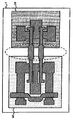
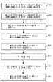
- CMOSデバイスを製作する方法であって、
PFETを収容するために半導体基板の中にNウェル領域を形成するステップと、
NFETを収容するために前記半導体基板の中にPウェル領域を形成するステップと、
前記PFETおよび前記NFETのいずれか一方をマスクで遮蔽するステップと、
前記マスクで遮蔽されていない前記PFETまたは前記NFETの上に第1の金属層を堆積させるステップと、
前記第1の金属層が堆積された前記PFETまたは前記NFETのゲート領域、ソース領域およびドレイン領域の上で第1のサリサイド形成を行うステップと、
前記マスクを除去するステップと、
前記PFETおよび前記NFETの上に前記第1の金属層とは異なる材料からなる第2の金属層を堆積させるステップと、
前記第1のサリサイドが形成されていない前記PFETまたは前記NFETのゲート領域、ソース領域およびドレイン領域の上で第2のサリサイド形成を行うステップと、を含む方法。 - 前記第1の金属層を堆積させるステップに続いて、前記第1の金属層の上にキャップ層を形成するステップをさらに含む、請求項1に記載の方法。
- 前記第2の金属層を堆積させるステップに続いて、前記第2の金属層の上にキャップ層を形成するステップをさらに含む、請求項2に記載の方法。
- 前記キャップ層は、TiN、Ti、及びTaNのいずれかを含む、請求項2または3に記載の方法。
- 前記第1の金属層及び前記第2の金属層は、Ti、Co、Ni、Pt、Re、W、Pd、Ta、Nb、及びこれらの合金の中から選択される、請求項1〜4のいずれか1項に記載の方法。
Applications Claiming Priority (3)
| Application Number | Priority Date | Filing Date | Title |
|---|---|---|---|
| US10/904,884 | 2004-12-02 | ||
| US10/904,884 US7064025B1 (en) | 2004-12-02 | 2004-12-02 | Method for forming self-aligned dual salicide in CMOS technologies |
| PCT/US2005/043474 WO2006060575A2 (en) | 2004-12-02 | 2005-12-01 | Method for forming self-aligned dual salicide in cmos technologies |
Publications (3)
| Publication Number | Publication Date |
|---|---|
| JP2008522444A JP2008522444A (ja) | 2008-06-26 |
| JP2008522444A5 JP2008522444A5 (ja) | 2008-10-09 |
| JP5102628B2 true JP5102628B2 (ja) | 2012-12-19 |
Family
ID=36565727
Family Applications (1)
| Application Number | Title | Priority Date | Filing Date |
|---|---|---|---|
| JP2007544510A Expired - Fee Related JP5102628B2 (ja) | 2004-12-02 | 2005-12-01 | Cmos技術における自己整合デュアル・サリサイド形成のための方法 |
Country Status (7)
| Country | Link |
|---|---|
| US (3) | US7064025B1 (ja) |
| EP (1) | EP1825508A4 (ja) |
| JP (1) | JP5102628B2 (ja) |
| KR (1) | KR101055708B1 (ja) |
| CN (1) | CN101069281B (ja) |
| TW (1) | TWI371084B (ja) |
| WO (1) | WO2006060575A2 (ja) |
Families Citing this family (26)
| Publication number | Priority date | Publication date | Assignee | Title |
|---|---|---|---|---|
| US7229909B2 (en) * | 2004-12-09 | 2007-06-12 | International Business Machines Corporation | Integrated circuit chip utilizing dielectric layer having oriented cylindrical voids formed from carbon nanotubes |
| US7446062B2 (en) * | 2004-12-10 | 2008-11-04 | International Business Machines Corporation | Device having dual etch stop liner and reformed silicide layer and related methods |
| WO2007057048A1 (en) * | 2005-11-21 | 2007-05-24 | Freescale Semiconductor, Inc. | Method for forming a semiconductor device having a salicide layer |
| US20070123042A1 (en) * | 2005-11-28 | 2007-05-31 | International Business Machines Corporation | Methods to form heterogeneous silicides/germanides in cmos technology |
| US7544575B2 (en) * | 2006-01-19 | 2009-06-09 | Freescale Semiconductor, Inc. | Dual metal silicide scheme using a dual spacer process |
| US20070178683A1 (en) * | 2006-02-02 | 2007-08-02 | Texas Instruments, Incorporated | Semiconductive device fabricated using a two step approach to silicide a gate and source/drains |
| DE102006015090B4 (de) * | 2006-03-31 | 2008-03-13 | Advanced Micro Devices, Inc., Sunnyvale | Verfahren zur Herstellung unterschiedlicher eingebetteter Verformungsschichten in Transistoren |
| JP2008112857A (ja) * | 2006-10-30 | 2008-05-15 | Nec Electronics Corp | 半導体集積回路装置 |
| US7750426B2 (en) * | 2007-05-30 | 2010-07-06 | Intersil Americas, Inc. | Junction barrier Schottky diode with dual silicides |
| US7569446B2 (en) * | 2007-06-12 | 2009-08-04 | International Business Machines Corporation | Semiconductor structure and method of manufacture |
| KR101406226B1 (ko) * | 2008-05-07 | 2014-06-13 | 삼성전자주식회사 | 반도체 소자의 제조 방법 |
| WO2009153880A1 (ja) * | 2008-06-20 | 2009-12-23 | 日本ユニサンティスエレクトロニクス株式会社 | 半導体記憶装置 |
| US20100019327A1 (en) * | 2008-07-22 | 2010-01-28 | Eun Jong Shin | Semiconductor Device and Method of Fabricating the Same |
| US8021971B2 (en) * | 2009-11-04 | 2011-09-20 | International Business Machines Corporation | Structure and method to form a thermally stable silicide in narrow dimension gate stacks |
| CN103456691B (zh) * | 2012-05-29 | 2015-07-29 | 中芯国际集成电路制造(上海)有限公司 | Cmos的制造方法 |
| KR20140101218A (ko) | 2013-02-08 | 2014-08-19 | 삼성전자주식회사 | 반도체 소자 및 그 제조 방법 |
| KR20140108960A (ko) | 2013-03-04 | 2014-09-15 | 삼성전자주식회사 | 듀얼 금속 실리사이드층을 갖는 반도체 장치의 제조 방법 |
| US8999799B2 (en) | 2013-08-29 | 2015-04-07 | International Business Machines Corporation | Maskless dual silicide contact formation |
| FR3016235B1 (fr) | 2014-01-08 | 2016-01-22 | Commissariat Energie Atomique | Procede de fabrication d'un dispositif microelectronique |
| US10546856B2 (en) | 2014-02-25 | 2020-01-28 | Stmicroelectronics, Inc. | CMOS structure having low resistance contacts and fabrication method |
| US9390981B1 (en) | 2015-02-05 | 2016-07-12 | Globalfoundries Inc. | Method of forming a complementary metal oxide semiconductor structure with N-type and P-type field effect transistors having symmetric source/drain junctions and optional dual silicides |
| US9564372B2 (en) | 2015-06-16 | 2017-02-07 | International Business Machines Corporation | Dual liner silicide |
| US9805973B2 (en) | 2015-10-30 | 2017-10-31 | International Business Machines Corporation | Dual silicide liner flow for enabling low contact resistance |
| US11443949B2 (en) * | 2019-03-20 | 2022-09-13 | Tokyo Electron Limited | Method of selectively forming metal silicides for semiconductor devices |
| TWI696270B (zh) * | 2019-04-15 | 2020-06-11 | 力晶積成電子製造股份有限公司 | 記憶體結構及其製造方法 |
| US20230187282A1 (en) * | 2021-12-15 | 2023-06-15 | Applied Materials, Inc. | Dual silicide process using ruthenium silicide |
Family Cites Families (30)
| Publication number | Priority date | Publication date | Assignee | Title |
|---|---|---|---|---|
| US4599789A (en) * | 1984-06-15 | 1986-07-15 | Harris Corporation | Process of making twin well VLSI CMOS |
| JPH04349660A (ja) * | 1991-05-28 | 1992-12-04 | Toshiba Corp | 半導体装置及び製造方法 |
| US5635426A (en) * | 1993-08-26 | 1997-06-03 | Fujitsu Limited | Method of making a semiconductor device having a silicide local interconnect |
| US5710450A (en) * | 1994-12-23 | 1998-01-20 | Intel Corporation | Transistor with ultra shallow tip and method of fabrication |
| US5770490A (en) * | 1996-08-29 | 1998-06-23 | International Business Machines Corporation | Method for producing dual work function CMOS device |
| US5824578A (en) * | 1996-12-12 | 1998-10-20 | Mosel Vitelic Inc. | Method of making a CMOS transistor using liquid phase deposition |
| US5989950A (en) * | 1998-01-26 | 1999-11-23 | Texas Instruments - Acer Incorporated | Reduced mask CMOS salicided process |
| US6100173A (en) | 1998-07-15 | 2000-08-08 | Advanced Micro Devices, Inc. | Forming a self-aligned silicide gate conductor to a greater thickness than junction silicide structures using a dual-salicidation process |
| JP2000286411A (ja) * | 1999-03-29 | 2000-10-13 | Toshiba Corp | 半導体装置とその製造方法 |
| US6277683B1 (en) * | 2000-02-28 | 2001-08-21 | Chartered Semiconductor Manufacturing Ltd. | Method of forming a sidewall spacer and a salicide blocking shape, using only one silicon nitride layer |
| US6562718B1 (en) | 2000-12-06 | 2003-05-13 | Advanced Micro Devices, Inc. | Process for forming fully silicided gates |
| JP3614782B2 (ja) * | 2001-01-19 | 2005-01-26 | シャープ株式会社 | 半導体装置の製造方法及びその方法により製造される半導体装置 |
| JP2002231908A (ja) * | 2001-02-06 | 2002-08-16 | Mitsubishi Electric Corp | 半導体装置の製造方法 |
| US6524939B2 (en) | 2001-02-23 | 2003-02-25 | Vanguard International Semiconductor Corporation | Dual salicidation process |
| US6528402B2 (en) | 2001-02-23 | 2003-03-04 | Vanguard International Semiconductor Corporation | Dual salicidation process |
| US6534405B1 (en) | 2001-10-01 | 2003-03-18 | Taiwan Semiconductor Manufacturing Company | Method of forming a MOSFET device featuring a dual salicide process |
| JP2005519468A (ja) * | 2002-02-28 | 2005-06-30 | アドバンスト・マイクロ・ディバイシズ・インコーポレイテッド | 半導体デバイス中の異なるシリコン含有領域上に、異なるシリサイド部分を形成する方法 |
| DE10208728B4 (de) * | 2002-02-28 | 2009-05-07 | Advanced Micro Devices, Inc., Sunnyvale | Ein Verfahren zur Herstellung eines Halbleiterelements mit unterschiedlichen Metallsilizidbereichen |
| DE10209059B4 (de) * | 2002-03-01 | 2007-04-05 | Advanced Micro Devices, Inc., Sunnyvale | Ein Halbleiterelement mit unterschiedlichen Metall-Halbleiterbereichen, die auf einem Halbleitergebiet gebildet sind, und Verfahren zur Herstellung des Halbleiterelements |
| US6787464B1 (en) * | 2002-07-02 | 2004-09-07 | Advanced Micro Devices, Inc. | Method of forming silicide layers over a plurality of semiconductor devices |
| KR100460268B1 (ko) * | 2002-07-16 | 2004-12-08 | 매그나칩 반도체 유한회사 | 비대칭 실리사이드막을 갖는 sram의 구조 및 그 제조방법 |
| US6894353B2 (en) * | 2002-07-31 | 2005-05-17 | Freescale Semiconductor, Inc. | Capped dual metal gate transistors for CMOS process and method for making the same |
| US6589836B1 (en) | 2002-10-03 | 2003-07-08 | Taiwan Semiconductor Manufacturing Company | One step dual salicide formation for ultra shallow junction applications |
| JP3921437B2 (ja) * | 2002-10-17 | 2007-05-30 | 富士通株式会社 | 半導体装置の製造方法 |
| JP4197607B2 (ja) * | 2002-11-06 | 2008-12-17 | 株式会社東芝 | 絶縁ゲート型電界効果トランジスタを含む半導体装置の製造方法 |
| US6846734B2 (en) * | 2002-11-20 | 2005-01-25 | International Business Machines Corporation | Method and process to make multiple-threshold metal gates CMOS technology |
| JP4209206B2 (ja) * | 2003-01-14 | 2009-01-14 | 富士通マイクロエレクトロニクス株式会社 | 半導体装置の製造方法 |
| US6891192B2 (en) * | 2003-08-04 | 2005-05-10 | International Business Machines Corporation | Structure and method of making strained semiconductor CMOS transistors having lattice-mismatched semiconductor regions underlying source and drain regions |
| US6905922B2 (en) * | 2003-10-03 | 2005-06-14 | Taiwan Semiconductor Manufacturing Company, Ltd. | Dual fully-silicided gate MOSFETs |
| US6982196B2 (en) * | 2003-11-04 | 2006-01-03 | International Business Machines Corporation | Oxidation method for altering a film structure and CMOS transistor structure formed therewith |
-
2004
- 2004-12-02 US US10/904,884 patent/US7064025B1/en active Active
-
2005
- 2005-10-20 US US11/254,929 patent/US7112481B2/en not_active Expired - Fee Related
- 2005-10-20 US US11/254,934 patent/US7067368B1/en active Active
- 2005-11-28 TW TW094141765A patent/TWI371084B/zh not_active IP Right Cessation
- 2005-12-01 KR KR1020077012730A patent/KR101055708B1/ko not_active IP Right Cessation
- 2005-12-01 EP EP05852638A patent/EP1825508A4/en not_active Withdrawn
- 2005-12-01 CN CN2005800413925A patent/CN101069281B/zh not_active Expired - Fee Related
- 2005-12-01 JP JP2007544510A patent/JP5102628B2/ja not_active Expired - Fee Related
- 2005-12-01 WO PCT/US2005/043474 patent/WO2006060575A2/en active Application Filing
Also Published As
| Publication number | Publication date |
|---|---|
| TW200625540A (en) | 2006-07-16 |
| US20060121665A1 (en) | 2006-06-08 |
| WO2006060575A3 (en) | 2007-04-26 |
| TWI371084B (en) | 2012-08-21 |
| CN101069281A (zh) | 2007-11-07 |
| US7112481B2 (en) | 2006-09-26 |
| US20060121662A1 (en) | 2006-06-08 |
| US20060121664A1 (en) | 2006-06-08 |
| EP1825508A4 (en) | 2009-06-24 |
| CN101069281B (zh) | 2012-05-30 |
| EP1825508A2 (en) | 2007-08-29 |
| US7067368B1 (en) | 2006-06-27 |
| JP2008522444A (ja) | 2008-06-26 |
| KR20070085805A (ko) | 2007-08-27 |
| KR101055708B1 (ko) | 2011-08-11 |
| US7064025B1 (en) | 2006-06-20 |
| WO2006060575A2 (en) | 2006-06-08 |
Similar Documents
| Publication | Publication Date | Title |
|---|---|---|
| JP5102628B2 (ja) | Cmos技術における自己整合デュアル・サリサイド形成のための方法 | |
| JP2008522443A (ja) | Cmosデバイスにおいて自己整合デュアル・フルシリサイド・ゲートを形成するための方法 | |
| US6806534B2 (en) | Damascene method for improved MOS transistor | |
| US6720630B2 (en) | Structure and method for MOSFET with metallic gate electrode | |
| US8159038B2 (en) | Self aligned silicided contacts | |
| US20090050972A1 (en) | Strained Semiconductor Device and Method of Making Same | |
| JP4826914B2 (ja) | 集積化金属珪化物ゲート電極を有するトランジスタの形成方法 | |
| US8115194B2 (en) | Semiconductor device capable of providing identical strains to each channel region of the transistors | |
| JP2005167252A (ja) | 集積回路構造体 | |
| JP2003174101A (ja) | 半導体装置および半導体装置の製造方法 | |
| US7563700B2 (en) | Method for improving self-aligned silicide extendibility with spacer recess using an aggregated spacer recess etch (ASRE) integration | |
| US20100197089A1 (en) | Methods of fabricating semiconductor devices with metal-semiconductor compound source/drain contact regions | |
| JP2004096041A (ja) | 半導体装置およびその製造方法 | |
| JP3762378B2 (ja) | 半導体装置及びその製造方法 | |
| JP2005109389A (ja) | 半導体装置及びその製造方法 | |
| JP2006352127A (ja) | 複数の熱処理によって自己整列されたシリサイド膜を形成する方法 | |
| JP2006140290A (ja) | 半導体装置およびその製造方法 | |
| KR100613585B1 (ko) | 반도체 소자의 제조 방법 | |
| CN113782426A (zh) | 半导体结构及其形成方法 | |
| US20110095381A1 (en) | Gate structure and method for making same | |
| KR20100077638A (ko) | 반도체 소자의 제조 방법 | |
| JP2006196561A (ja) | 半導体装置の製造方法 | |
| KR20100026821A (ko) | 반도체 소자 제조 방법 | |
| JP2006278925A (ja) | 半導体装置の製造方法 |
Legal Events
| Date | Code | Title | Description |
|---|---|---|---|
| A521 | Request for written amendment filed |
Free format text: JAPANESE INTERMEDIATE CODE: A523 Effective date: 20080822 |
|
| A621 | Written request for application examination |
Free format text: JAPANESE INTERMEDIATE CODE: A621 Effective date: 20080822 |
|
| A131 | Notification of reasons for refusal |
Free format text: JAPANESE INTERMEDIATE CODE: A131 Effective date: 20120214 |
|
| A521 | Request for written amendment filed |
Free format text: JAPANESE INTERMEDIATE CODE: A523 Effective date: 20120430 |
|
| RD12 | Notification of acceptance of power of sub attorney |
Free format text: JAPANESE INTERMEDIATE CODE: A7432 Effective date: 20120430 |
|
| A521 | Request for written amendment filed |
Free format text: JAPANESE INTERMEDIATE CODE: A821 Effective date: 20120501 |
|
| A131 | Notification of reasons for refusal |
Free format text: JAPANESE INTERMEDIATE CODE: A131 Effective date: 20120612 |
|
| A521 | Request for written amendment filed |
Free format text: JAPANESE INTERMEDIATE CODE: A523 Effective date: 20120730 |
|
| TRDD | Decision of grant or rejection written | ||
| A01 | Written decision to grant a patent or to grant a registration (utility model) |
Free format text: JAPANESE INTERMEDIATE CODE: A01 Effective date: 20120904 |
|
| RD14 | Notification of resignation of power of sub attorney |
Free format text: JAPANESE INTERMEDIATE CODE: A7434 Effective date: 20120904 |
|
| A01 | Written decision to grant a patent or to grant a registration (utility model) |
Free format text: JAPANESE INTERMEDIATE CODE: A01 |
|
| A61 | First payment of annual fees (during grant procedure) |
Free format text: JAPANESE INTERMEDIATE CODE: A61 Effective date: 20120928 |
|
| FPAY | Renewal fee payment (event date is renewal date of database) |
Free format text: PAYMENT UNTIL: 20151005 Year of fee payment: 3 |
|
| R150 | Certificate of patent or registration of utility model |
Ref document number: 5102628 Country of ref document: JP Free format text: JAPANESE INTERMEDIATE CODE: R150 Free format text: JAPANESE INTERMEDIATE CODE: R150 |
|
| R250 | Receipt of annual fees |
Free format text: JAPANESE INTERMEDIATE CODE: R250 |
|
| R250 | Receipt of annual fees |
Free format text: JAPANESE INTERMEDIATE CODE: R250 |
|
| R250 | Receipt of annual fees |
Free format text: JAPANESE INTERMEDIATE CODE: R250 |
|
| R250 | Receipt of annual fees |
Free format text: JAPANESE INTERMEDIATE CODE: R250 |
|
| R250 | Receipt of annual fees |
Free format text: JAPANESE INTERMEDIATE CODE: R250 |
|
| R250 | Receipt of annual fees |
Free format text: JAPANESE INTERMEDIATE CODE: R250 |
|
| LAPS | Cancellation because of no payment of annual fees |