JP5026257B2 - 電子装置 - Google Patents
電子装置 Download PDFInfo
- Publication number
- JP5026257B2 JP5026257B2 JP2007512641A JP2007512641A JP5026257B2 JP 5026257 B2 JP5026257 B2 JP 5026257B2 JP 2007512641 A JP2007512641 A JP 2007512641A JP 2007512641 A JP2007512641 A JP 2007512641A JP 5026257 B2 JP5026257 B2 JP 5026257B2
- Authority
- JP
- Japan
- Prior art keywords
- substrate
- electronic device
- pin diode
- layer
- pin
- Prior art date
- Legal status (The legal status is an assumption and is not a legal conclusion. Google has not performed a legal analysis and makes no representation as to the accuracy of the status listed.)
- Expired - Fee Related
Links
- 239000000758 substrate Substances 0.000 claims abstract description 70
- 239000003990 capacitor Substances 0.000 claims abstract description 32
- 239000000463 material Substances 0.000 claims abstract description 7
- 239000004065 semiconductor Substances 0.000 claims abstract description 5
- 239000002344 surface layer Substances 0.000 claims abstract description 3
- 239000010409 thin film Substances 0.000 claims abstract description 3
- 239000010410 layer Substances 0.000 claims description 74
- 230000005540 biological transmission Effects 0.000 claims description 12
- 238000002955 isolation Methods 0.000 claims description 6
- 239000002245 particle Substances 0.000 claims description 5
- 125000006850 spacer group Chemical group 0.000 claims description 4
- 239000013078 crystal Substances 0.000 claims description 3
- 230000005670 electromagnetic radiation Effects 0.000 claims description 3
- 239000010408 film Substances 0.000 description 9
- 230000008901 benefit Effects 0.000 description 8
- XUIMIQQOPSSXEZ-UHFFFAOYSA-N Silicon Chemical compound [Si] XUIMIQQOPSSXEZ-UHFFFAOYSA-N 0.000 description 7
- 229910052710 silicon Inorganic materials 0.000 description 7
- 239000010703 silicon Substances 0.000 description 7
- 230000005855 radiation Effects 0.000 description 6
- 238000002513 implantation Methods 0.000 description 5
- 230000010354 integration Effects 0.000 description 5
- 238000005468 ion implantation Methods 0.000 description 5
- 238000000034 method Methods 0.000 description 5
- XKRFYHLGVUSROY-UHFFFAOYSA-N Argon Chemical compound [Ar] XKRFYHLGVUSROY-UHFFFAOYSA-N 0.000 description 4
- IJGRMHOSHXDMSA-UHFFFAOYSA-N Atomic nitrogen Chemical compound N#N IJGRMHOSHXDMSA-UHFFFAOYSA-N 0.000 description 4
- 229910008065 Si-SiO Inorganic materials 0.000 description 4
- 229910006405 Si—SiO Inorganic materials 0.000 description 4
- XAGFODPZIPBFFR-UHFFFAOYSA-N aluminium Chemical compound [Al] XAGFODPZIPBFFR-UHFFFAOYSA-N 0.000 description 4
- 229910052782 aluminium Inorganic materials 0.000 description 4
- 239000003989 dielectric material Substances 0.000 description 4
- 238000010894 electron beam technology Methods 0.000 description 4
- 230000007547 defect Effects 0.000 description 3
- 238000010586 diagram Methods 0.000 description 3
- 230000000694 effects Effects 0.000 description 3
- 239000012777 electrically insulating material Substances 0.000 description 3
- 150000002500 ions Chemical class 0.000 description 3
- PXHVJJICTQNCMI-UHFFFAOYSA-N Nickel Chemical compound [Ni] PXHVJJICTQNCMI-UHFFFAOYSA-N 0.000 description 2
- VYPSYNLAJGMNEJ-UHFFFAOYSA-N Silicium dioxide Chemical compound O=[Si]=O VYPSYNLAJGMNEJ-UHFFFAOYSA-N 0.000 description 2
- 229910052786 argon Inorganic materials 0.000 description 2
- 230000015556 catabolic process Effects 0.000 description 2
- 239000004020 conductor Substances 0.000 description 2
- 230000008021 deposition Effects 0.000 description 2
- 238000005530 etching Methods 0.000 description 2
- 238000010438 heat treatment Methods 0.000 description 2
- 230000001939 inductive effect Effects 0.000 description 2
- 238000002347 injection Methods 0.000 description 2
- 239000007924 injection Substances 0.000 description 2
- 239000012212 insulator Substances 0.000 description 2
- 238000004519 manufacturing process Methods 0.000 description 2
- 229910052757 nitrogen Inorganic materials 0.000 description 2
- 230000003071 parasitic effect Effects 0.000 description 2
- BASFCYQUMIYNBI-UHFFFAOYSA-N platinum Chemical compound [Pt] BASFCYQUMIYNBI-UHFFFAOYSA-N 0.000 description 2
- 230000008569 process Effects 0.000 description 2
- 238000012545 processing Methods 0.000 description 2
- 229910021332 silicide Inorganic materials 0.000 description 2
- FVBUAEGBCNSCDD-UHFFFAOYSA-N silicide(4-) Chemical group [Si-4] FVBUAEGBCNSCDD-UHFFFAOYSA-N 0.000 description 2
- 229910052814 silicon oxide Inorganic materials 0.000 description 2
- 229910000838 Al alloy Inorganic materials 0.000 description 1
- 241000282461 Canis lupus Species 0.000 description 1
- RYGMFSIKBFXOCR-UHFFFAOYSA-N Copper Chemical compound [Cu] RYGMFSIKBFXOCR-UHFFFAOYSA-N 0.000 description 1
- ZOKXTWBITQBERF-UHFFFAOYSA-N Molybdenum Chemical compound [Mo] ZOKXTWBITQBERF-UHFFFAOYSA-N 0.000 description 1
- RTAQQCXQSZGOHL-UHFFFAOYSA-N Titanium Chemical compound [Ti] RTAQQCXQSZGOHL-UHFFFAOYSA-N 0.000 description 1
- 238000009825 accumulation Methods 0.000 description 1
- 230000002411 adverse Effects 0.000 description 1
- 229910021417 amorphous silicon Inorganic materials 0.000 description 1
- 230000003321 amplification Effects 0.000 description 1
- QVGXLLKOCUKJST-UHFFFAOYSA-N atomic oxygen Chemical compound [O] QVGXLLKOCUKJST-UHFFFAOYSA-N 0.000 description 1
- 230000009286 beneficial effect Effects 0.000 description 1
- 230000015572 biosynthetic process Effects 0.000 description 1
- 230000008859 change Effects 0.000 description 1
- 239000002800 charge carrier Substances 0.000 description 1
- 229910017052 cobalt Inorganic materials 0.000 description 1
- 239000010941 cobalt Substances 0.000 description 1
- GUTLYIVDDKVIGB-UHFFFAOYSA-N cobalt atom Chemical compound [Co] GUTLYIVDDKVIGB-UHFFFAOYSA-N 0.000 description 1
- 230000000295 complement effect Effects 0.000 description 1
- 238000010276 construction Methods 0.000 description 1
- 229910052802 copper Inorganic materials 0.000 description 1
- 239000010949 copper Substances 0.000 description 1
- 230000008878 coupling Effects 0.000 description 1
- 238000010168 coupling process Methods 0.000 description 1
- 238000005859 coupling reaction Methods 0.000 description 1
- 238000002484 cyclic voltammetry Methods 0.000 description 1
- 238000013461 design Methods 0.000 description 1
- 238000009792 diffusion process Methods 0.000 description 1
- 238000001312 dry etching Methods 0.000 description 1
- 230000005684 electric field Effects 0.000 description 1
- 238000009713 electroplating Methods 0.000 description 1
- 230000003090 exacerbative effect Effects 0.000 description 1
- 238000001914 filtration Methods 0.000 description 1
- 239000011521 glass Substances 0.000 description 1
- PCHJSUWPFVWCPO-UHFFFAOYSA-N gold Chemical compound [Au] PCHJSUWPFVWCPO-UHFFFAOYSA-N 0.000 description 1
- 229910052737 gold Inorganic materials 0.000 description 1
- 239000010931 gold Substances 0.000 description 1
- 239000001307 helium Substances 0.000 description 1
- 229910052734 helium Inorganic materials 0.000 description 1
- SWQJXJOGLNCZEY-UHFFFAOYSA-N helium atom Chemical compound [He] SWQJXJOGLNCZEY-UHFFFAOYSA-N 0.000 description 1
- 239000012535 impurity Substances 0.000 description 1
- 238000001802 infusion Methods 0.000 description 1
- 238000003780 insertion Methods 0.000 description 1
- 230000037431 insertion Effects 0.000 description 1
- 238000005259 measurement Methods 0.000 description 1
- 230000004048 modification Effects 0.000 description 1
- 238000012986 modification Methods 0.000 description 1
- 229910052750 molybdenum Inorganic materials 0.000 description 1
- 239000011733 molybdenum Substances 0.000 description 1
- 229910052759 nickel Inorganic materials 0.000 description 1
- 150000004767 nitrides Chemical class 0.000 description 1
- 238000003199 nucleic acid amplification method Methods 0.000 description 1
- 239000001301 oxygen Substances 0.000 description 1
- 229910052760 oxygen Inorganic materials 0.000 description 1
- 230000035515 penetration Effects 0.000 description 1
- 229910052697 platinum Inorganic materials 0.000 description 1
- 229910021420 polycrystalline silicon Inorganic materials 0.000 description 1
- 229920005591 polysilicon Polymers 0.000 description 1
- 239000011241 protective layer Substances 0.000 description 1
- 230000006798 recombination Effects 0.000 description 1
- 238000000926 separation method Methods 0.000 description 1
- 230000008054 signal transmission Effects 0.000 description 1
- LIVNPJMFVYWSIS-UHFFFAOYSA-N silicon monoxide Chemical compound [Si-]#[O+] LIVNPJMFVYWSIS-UHFFFAOYSA-N 0.000 description 1
- 238000003746 solid phase reaction Methods 0.000 description 1
- 230000001629 suppression Effects 0.000 description 1
- 229910052719 titanium Inorganic materials 0.000 description 1
- 239000010936 titanium Substances 0.000 description 1
- 238000001039 wet etching Methods 0.000 description 1
Images


Classifications
-
- H—ELECTRICITY
- H03—ELECTRONIC CIRCUITRY
- H03H—IMPEDANCE NETWORKS, e.g. RESONANT CIRCUITS; RESONATORS
- H03H3/00—Apparatus or processes specially adapted for the manufacture of impedance networks, resonating circuits, resonators
-
- H—ELECTRICITY
- H03—ELECTRONIC CIRCUITRY
- H03H—IMPEDANCE NETWORKS, e.g. RESONANT CIRCUITS; RESONATORS
- H03H7/00—Multiple-port networks comprising only passive electrical elements as network components
- H03H7/01—Frequency selective two-port networks
- H03H7/0123—Frequency selective two-port networks comprising distributed impedance elements together with lumped impedance elements
-
- H—ELECTRICITY
- H10—SEMICONDUCTOR DEVICES; ELECTRIC SOLID-STATE DEVICES NOT OTHERWISE PROVIDED FOR
- H10D—INORGANIC ELECTRIC SEMICONDUCTOR DEVICES
- H10D84/00—Integrated devices formed in or on semiconductor substrates that comprise only semiconducting layers, e.g. on Si wafers or on GaAs-on-Si wafers
- H10D84/201—Integrated devices formed in or on semiconductor substrates that comprise only semiconducting layers, e.g. on Si wafers or on GaAs-on-Si wafers characterised by the integration of only components covered by H10D1/00 or H10D8/00, e.g. RLC circuits
- H10D84/204—Integrated devices formed in or on semiconductor substrates that comprise only semiconducting layers, e.g. on Si wafers or on GaAs-on-Si wafers characterised by the integration of only components covered by H10D1/00 or H10D8/00, e.g. RLC circuits of combinations of diodes or capacitors or resistors
- H10D84/221—Integrated devices formed in or on semiconductor substrates that comprise only semiconducting layers, e.g. on Si wafers or on GaAs-on-Si wafers characterised by the integration of only components covered by H10D1/00 or H10D8/00, e.g. RLC circuits of combinations of diodes or capacitors or resistors of only diodes
Landscapes
- Engineering & Computer Science (AREA)
- Manufacturing & Machinery (AREA)
- Semiconductor Integrated Circuits (AREA)
- Liquid Crystal Substances (AREA)
- Glass Compositions (AREA)
- Sheets, Magazines, And Separation Thereof (AREA)
Description
Claims (11)
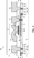
- 半導体材料の基板の第1の面上に少なくとも1つの薄膜キャパシタ及び少なくとも1つのインダクタの回路網を含み、前記基板は、前記インダクタの電気的損失を制限するための100Ω・cm以上の高抵抗を有し、前記第1の面上の電気絶縁表面層を備え、
第1及び第2の横型PINダイオードは前記基板に画定され、前記PINダイオードが互いにp導電型領域、n導電型領域、及び中間真性領域を有し、前記PINダイオードのうち前記第1のPINダイオードの前記真性領域の幅は前記第2のPINダイオードの真性領域の幅よりも大きく、前記インダクタと前記キャパシタは2つのPINダイオード間に横方向に存在し、前記第1のPINダイオードは受信パス用ダイオードを構成し、前記第2のPINダイオードは送信パス用ダイオードを構成する、電子装置。 - 請求項1に記載の電子装置であって、前記基板は、前記第1と前記第2のPINダイオードの間のクロストークを防ぐ手段を備える電子装置。
- 請求項2に記載の電子装置であって、前記クロストークを防ぐ手段は、前記第1のPINダイオードが画定される基板部分のアイソレーションを含み、前記アイソレーションは、前記基板の埋め込み層と前記埋め込み層から前記基板表面へ延伸するリング状側壁を含み、前記基板部分は、他の基板部分から電気的に絶縁される電子装置。
- 請求項2に記載の電子装置であって、前記クロストークを防ぐ手段は、粒子の電磁放射線のビームによる前記基板の部分的な照射により得られる前記結晶格子に対するダメージを引き起こす電子装置。
- 請求項2に記載の電子装置であって、前記クロストークを防ぐ手段は、電気導電粒子を含む電子装置。
- 請求項1に記載の電子装置であって、前記第1のPINダイオードは、前記基板表面に対して平行な断面において、円形又は楕円形を有する電子装置。
- 請求項6に記載の電子装置であって、前記n導電型領域は、前記真性領域の内部に横方向に存在する電子装置。
- 請求項6又は7に記載の電子装置であって、前記円形又は楕円形はギャップを備え、前記第1のPINダイオードの領域を接続するための相互接続は、前記基板表面上の前記相互接続の垂直射影上に前記ギャップに重なるように配置される電子装置。
- 請求項1に記載の電子装置であって、前記コイル及び前記キャパシタは、第1及び第2の電気導電層、誘電層、並びにそれらの間の絶縁層を含む束に埋め込まれ、前記絶縁層は、スペーサとして機能し、前記キャパシタの電極を接続するためのコンタクトウインドウを含む電子装置。
- 請求項1に記載の電子装置であって、前記第1のPINダイオードは、受信パスのアンテナスイッチとして用いられ、前記第2のPINダイオードは、送信パスのアンテナスイッチとして用いられる電子装置。
- 請求項9に記載の電子装置であって、受動素子の前記回路網は、インピーダンスマッチング回路網として用いられる電子装置。
Applications Claiming Priority (3)
| Application Number | Priority Date | Filing Date | Title |
|---|---|---|---|
| EP04101966 | 2004-05-06 | ||
| EP04101966.2 | 2004-05-06 | ||
| PCT/IB2005/051433 WO2005109636A1 (en) | 2004-05-06 | 2005-05-03 | Electronic device |
Publications (2)
| Publication Number | Publication Date |
|---|---|
| JP2007536759A JP2007536759A (ja) | 2007-12-13 |
| JP5026257B2 true JP5026257B2 (ja) | 2012-09-12 |
Family
ID=34965733
Family Applications (1)
| Application Number | Title | Priority Date | Filing Date |
|---|---|---|---|
| JP2007512641A Expired - Fee Related JP5026257B2 (ja) | 2004-05-06 | 2005-05-03 | 電子装置 |
Country Status (7)
| Country | Link |
|---|---|
| US (1) | US8901703B2 (ja) |
| EP (1) | EP1745545B1 (ja) |
| JP (1) | JP5026257B2 (ja) |
| CN (1) | CN100533967C (ja) |
| AT (1) | ATE388520T1 (ja) |
| DE (1) | DE602005005189T2 (ja) |
| WO (1) | WO2005109636A1 (ja) |
Families Citing this family (8)
| Publication number | Priority date | Publication date | Assignee | Title |
|---|---|---|---|---|
| EP2024990B1 (en) * | 2006-05-18 | 2011-06-29 | Ipdia | Method of increasing the quality factor of an inductor in a semiconductor device |
| KR100747657B1 (ko) | 2006-10-26 | 2007-08-08 | 삼성전자주식회사 | 매크로 및 마이크로 주파수 튜닝이 가능한 반도체 소자 및이를 갖는 안테나와 주파수 튜닝 회로 |
| JP5399513B2 (ja) * | 2008-12-31 | 2014-01-29 | シエラ・ネバダ・コーポレイション | モノリシック半導体マイクロ波スイッチアレイ |
| US8237243B2 (en) | 2009-03-18 | 2012-08-07 | International Business Machines Corporation | On-chip capacitors with a variable capacitance for a radiofrequency integrated circuit |
| JP5481127B2 (ja) * | 2009-08-19 | 2014-04-23 | 株式会社ジャパンディスプレイ | センサ素子およびその駆動方法、センサ装置、ならびに入力機能付き表示装置および電子機器 |
| JP6425633B2 (ja) * | 2015-08-21 | 2018-11-21 | 住重アテックス株式会社 | 半導体装置および半導体装置の製造方法 |
| US12569639B2 (en) | 2020-01-21 | 2026-03-10 | Wearair Ventures, Inc. | Efficient enriched oxygen airflow systems and methods |
| US20210220599A1 (en) | 2020-01-21 | 2021-07-22 | Wearair Ventures, Inc. | Efficient enriched oxygen airflow systems and methods |
Family Cites Families (27)
| Publication number | Priority date | Publication date | Assignee | Title |
|---|---|---|---|---|
| US4474623A (en) * | 1982-04-26 | 1984-10-02 | Raytheon Company | Method of passivating a semiconductor body |
| US4810980A (en) * | 1987-06-04 | 1989-03-07 | Texas Instruments, Inc. | Matched variable attenuation switched limiter |
| US5280194A (en) * | 1988-11-21 | 1994-01-18 | Micro Technology Partners | Electrical apparatus with a metallic layer coupled to a lower region of a substrate and metallic layer coupled to a lower region of a semiconductor device |
| GB2228616B (en) | 1989-02-22 | 1992-11-04 | Stc Plc | Opto-electronic device |
| JP3120938B2 (ja) * | 1994-02-16 | 2000-12-25 | 松下電子工業株式会社 | 半導体集積装置およびその製造方法 |
| JP3959125B2 (ja) | 1994-09-14 | 2007-08-15 | 株式会社東芝 | 半導体装置 |
| DE19533206A1 (de) | 1995-09-08 | 1997-03-13 | Daimler Benz Ag | Planare PIN-Diode und Verfahren zu deren Herstellung |
| JPH09214278A (ja) * | 1996-01-30 | 1997-08-15 | Nec Corp | Pinダイオード可変減衰器 |
| TW392392B (en) | 1997-04-03 | 2000-06-01 | Lucent Technologies Inc | High frequency apparatus including a low loss substrate |
| US5986517A (en) | 1998-01-06 | 1999-11-16 | Trw Inc. | Low-loss air suspended radially combined patch for N-way RF switch |
| JP3309959B2 (ja) | 1998-04-16 | 2002-07-29 | 日本電気株式会社 | 半導体装置 |
| DE19821726C1 (de) * | 1998-05-14 | 1999-09-09 | Texas Instruments Deutschland | Ingegrierte CMOS-Schaltung für die Verwendung bei hohen Frequenzen |
| KR100697405B1 (ko) | 2000-02-15 | 2007-03-20 | 코닌클리즈케 필립스 일렉트로닉스 엔.브이. | 전자 디바이스 |
| EP1137055A1 (de) | 2000-03-24 | 2001-09-26 | Infineon Technologies AG | Verfahren zur Herstellung einer Hochfrequenz-Halbleiterstruktur und Hochfrequenz-Halbleiterstruktur |
| JP2001352079A (ja) | 2000-06-07 | 2001-12-21 | Nec Corp | ダイオードおよびその製造方法 |
| DE60140722D1 (de) | 2000-09-05 | 2010-01-21 | Nxp Bv | Integrierte elektromagnetische Abschirmvorrichtung |
| US6660616B2 (en) * | 2001-01-31 | 2003-12-09 | Texas Instruments Incorporated | P-i-n transit time silicon-on-insulator device |
| DE10127952A1 (de) * | 2001-06-08 | 2002-12-19 | Infineon Technologies Ag | Laterale PIN-Diode und Verfahren zur Herstellung derselben |
| JP4299488B2 (ja) | 2001-12-07 | 2009-07-22 | 太陽誘電株式会社 | 高周波モジュールおよびその製造方法 |
| US6620673B1 (en) * | 2002-03-08 | 2003-09-16 | Alpine Microsystems, Inc. | Thin film capacitor having multi-layer dielectric film including silicon dioxide and tantalum pentoxide |
| JP2004014658A (ja) | 2002-06-05 | 2004-01-15 | Renesas Technology Corp | 半導体装置およびその製造方法 |
| JP4004357B2 (ja) | 2002-08-29 | 2007-11-07 | 新電元工業株式会社 | ダイオード |
| WO2004036778A1 (en) | 2002-10-14 | 2004-04-29 | Koninklijke Philips Electronics N.V. | Transmit and receive antenna switch |
| US7132723B2 (en) * | 2002-11-14 | 2006-11-07 | Raytheon Company | Micro electro-mechanical system device with piezoelectric thin film actuator |
| WO2005008908A1 (en) | 2003-07-22 | 2005-01-27 | Koninklijke Philips Electronics N.V. | Antenna switch with adaptive filter |
| JP2007231072A (ja) | 2006-02-28 | 2007-09-13 | Three M Innovative Properties Co | コーティング組成物及びそれを使用した物品 |
| JP2009214278A (ja) | 2008-03-13 | 2009-09-24 | Nikon Corp | 研削用砥石 |
-
2005
- 2005-05-03 US US11/579,679 patent/US8901703B2/en not_active Expired - Lifetime
- 2005-05-03 WO PCT/IB2005/051433 patent/WO2005109636A1/en not_active Ceased
- 2005-05-03 DE DE602005005189T patent/DE602005005189T2/de not_active Expired - Lifetime
- 2005-05-03 EP EP05732041A patent/EP1745545B1/en not_active Expired - Lifetime
- 2005-05-03 JP JP2007512641A patent/JP5026257B2/ja not_active Expired - Fee Related
- 2005-05-03 CN CNB2005800141916A patent/CN100533967C/zh not_active Expired - Fee Related
- 2005-05-03 AT AT05732041T patent/ATE388520T1/de not_active IP Right Cessation
Also Published As
| Publication number | Publication date |
|---|---|
| ATE388520T1 (de) | 2008-03-15 |
| EP1745545B1 (en) | 2008-03-05 |
| US20070228514A1 (en) | 2007-10-04 |
| US8901703B2 (en) | 2014-12-02 |
| JP2007536759A (ja) | 2007-12-13 |
| WO2005109636A1 (en) | 2005-11-17 |
| EP1745545A1 (en) | 2007-01-24 |
| DE602005005189T2 (de) | 2009-03-19 |
| CN100533967C (zh) | 2009-08-26 |
| DE602005005189D1 (de) | 2008-04-17 |
| CN1951004A (zh) | 2007-04-18 |
Similar Documents
| Publication | Publication Date | Title |
|---|---|---|
| US8058689B2 (en) | Techniques to reduce substrate cross talk on mixed signal and RF circuit design | |
| KR100522655B1 (ko) | 기판 내에 매립된 패러데이 차폐와 유전체 웰을 갖는 높은q 값의 인덕터 | |
| KR101831219B1 (ko) | 수직 핀 다이오드의 제조방법 | |
| US6310387B1 (en) | Integrated circuit inductor with high self-resonance frequency | |
| US20090039457A1 (en) | Low crosstalk substrate for mixed-signal integrated circuits | |
| US6258688B1 (en) | Method to form a high Q inductor | |
| US6448604B1 (en) | Integrated adjustable capacitor | |
| CN101449362B (zh) | 提高半导体器件中电感器的品质因子的方法 | |
| JP2008516441A (ja) | 半導体デバイス及びその使用 | |
| JP5026257B2 (ja) | 電子装置 | |
| US7176546B2 (en) | Diode circuit and method of producing a diode circuit | |
| CN1947250B (zh) | 半导体器件和制造这种器件的方法 | |
| JP2004303744A (ja) | モノリシックマイクロ波集積回路およびその製造方法 | |
| US7902013B1 (en) | Method of forming a semiconductor die with reduced RF attenuation | |
| WO2021242972A1 (en) | Low-loss millimeter wave transmission lines on silicon substrate | |
| US9941353B2 (en) | Structure and method for mitigating substrate parasitics in bulk high resistivity substrate technology |
Legal Events
| Date | Code | Title | Description |
|---|---|---|---|
| A621 | Written request for application examination |
Free format text: JAPANESE INTERMEDIATE CODE: A621 Effective date: 20080502 |
|
| A711 | Notification of change in applicant |
Free format text: JAPANESE INTERMEDIATE CODE: A711 Effective date: 20080626 |
|
| A977 | Report on retrieval |
Free format text: JAPANESE INTERMEDIATE CODE: A971007 Effective date: 20111014 |
|
| A131 | Notification of reasons for refusal |
Free format text: JAPANESE INTERMEDIATE CODE: A131 Effective date: 20111018 |
|
| A521 | Request for written amendment filed |
Free format text: JAPANESE INTERMEDIATE CODE: A523 Effective date: 20120113 |
|
| TRDD | Decision of grant or rejection written | ||
| A01 | Written decision to grant a patent or to grant a registration (utility model) |
Free format text: JAPANESE INTERMEDIATE CODE: A01 Effective date: 20120525 |
|
| A01 | Written decision to grant a patent or to grant a registration (utility model) |
Free format text: JAPANESE INTERMEDIATE CODE: A01 |
|
| A61 | First payment of annual fees (during grant procedure) |
Free format text: JAPANESE INTERMEDIATE CODE: A61 Effective date: 20120620 |
|
| FPAY | Renewal fee payment (event date is renewal date of database) |
Free format text: PAYMENT UNTIL: 20150629 Year of fee payment: 3 |
|
| R150 | Certificate of patent or registration of utility model |
Ref document number: 5026257 Country of ref document: JP Free format text: JAPANESE INTERMEDIATE CODE: R150 |
|
| R250 | Receipt of annual fees |
Free format text: JAPANESE INTERMEDIATE CODE: R250 |
|
| S111 | Request for change of ownership or part of ownership |
Free format text: JAPANESE INTERMEDIATE CODE: R313113 |
|
| R350 | Written notification of registration of transfer |
Free format text: JAPANESE INTERMEDIATE CODE: R350 |
|
| R250 | Receipt of annual fees |
Free format text: JAPANESE INTERMEDIATE CODE: R250 |
|
| R250 | Receipt of annual fees |
Free format text: JAPANESE INTERMEDIATE CODE: R250 |
|
| R250 | Receipt of annual fees |
Free format text: JAPANESE INTERMEDIATE CODE: R250 |
|
| R250 | Receipt of annual fees |
Free format text: JAPANESE INTERMEDIATE CODE: R250 |
|
| R250 | Receipt of annual fees |
Free format text: JAPANESE INTERMEDIATE CODE: R250 |
|
| R250 | Receipt of annual fees |
Free format text: JAPANESE INTERMEDIATE CODE: R250 |
|
| R250 | Receipt of annual fees |
Free format text: JAPANESE INTERMEDIATE CODE: R250 |
|
| LAPS | Cancellation because of no payment of annual fees |