JP5026257B2 - Electronic equipment - Google Patents
Electronic equipment Download PDFInfo
- Publication number
- JP5026257B2 JP5026257B2 JP2007512641A JP2007512641A JP5026257B2 JP 5026257 B2 JP5026257 B2 JP 5026257B2 JP 2007512641 A JP2007512641 A JP 2007512641A JP 2007512641 A JP2007512641 A JP 2007512641A JP 5026257 B2 JP5026257 B2 JP 5026257B2
- Authority
- JP
- Japan
- Prior art keywords
- substrate
- electronic device
- pin diode
- layer
- pin
- Prior art date
- Legal status (The legal status is an assumption and is not a legal conclusion. Google has not performed a legal analysis and makes no representation as to the accuracy of the status listed.)
- Expired - Fee Related
Links
- 239000000758 substrate Substances 0.000 claims abstract description 70
- 239000003990 capacitor Substances 0.000 claims abstract description 32
- 239000000463 material Substances 0.000 claims abstract description 7
- 239000004065 semiconductor Substances 0.000 claims abstract description 5
- 239000002344 surface layer Substances 0.000 claims abstract description 3
- 239000010409 thin film Substances 0.000 claims abstract description 3
- 239000010410 layer Substances 0.000 claims description 74
- 230000005540 biological transmission Effects 0.000 claims description 12
- 238000002955 isolation Methods 0.000 claims description 6
- 239000002245 particle Substances 0.000 claims description 5
- 125000006850 spacer group Chemical group 0.000 claims description 4
- 239000013078 crystal Substances 0.000 claims description 3
- 230000005670 electromagnetic radiation Effects 0.000 claims description 3
- 239000010408 film Substances 0.000 description 9
- 230000008901 benefit Effects 0.000 description 8
- XUIMIQQOPSSXEZ-UHFFFAOYSA-N Silicon Chemical compound [Si] XUIMIQQOPSSXEZ-UHFFFAOYSA-N 0.000 description 7
- 229910052710 silicon Inorganic materials 0.000 description 7
- 239000010703 silicon Substances 0.000 description 7
- 230000005855 radiation Effects 0.000 description 6
- 238000002513 implantation Methods 0.000 description 5
- 230000010354 integration Effects 0.000 description 5
- 238000005468 ion implantation Methods 0.000 description 5
- 238000000034 method Methods 0.000 description 5
- XKRFYHLGVUSROY-UHFFFAOYSA-N Argon Chemical compound [Ar] XKRFYHLGVUSROY-UHFFFAOYSA-N 0.000 description 4
- IJGRMHOSHXDMSA-UHFFFAOYSA-N Atomic nitrogen Chemical compound N#N IJGRMHOSHXDMSA-UHFFFAOYSA-N 0.000 description 4
- 229910008065 Si-SiO Inorganic materials 0.000 description 4
- 229910006405 Si—SiO Inorganic materials 0.000 description 4
- XAGFODPZIPBFFR-UHFFFAOYSA-N aluminium Chemical compound [Al] XAGFODPZIPBFFR-UHFFFAOYSA-N 0.000 description 4
- 229910052782 aluminium Inorganic materials 0.000 description 4
- 239000003989 dielectric material Substances 0.000 description 4
- 238000010894 electron beam technology Methods 0.000 description 4
- 230000007547 defect Effects 0.000 description 3
- 238000010586 diagram Methods 0.000 description 3
- 230000000694 effects Effects 0.000 description 3
- 239000012777 electrically insulating material Substances 0.000 description 3
- 150000002500 ions Chemical class 0.000 description 3
- PXHVJJICTQNCMI-UHFFFAOYSA-N Nickel Chemical compound [Ni] PXHVJJICTQNCMI-UHFFFAOYSA-N 0.000 description 2
- VYPSYNLAJGMNEJ-UHFFFAOYSA-N Silicium dioxide Chemical compound O=[Si]=O VYPSYNLAJGMNEJ-UHFFFAOYSA-N 0.000 description 2
- 229910052786 argon Inorganic materials 0.000 description 2
- 230000015556 catabolic process Effects 0.000 description 2
- 239000004020 conductor Substances 0.000 description 2
- 230000008021 deposition Effects 0.000 description 2
- 238000005530 etching Methods 0.000 description 2
- 238000010438 heat treatment Methods 0.000 description 2
- 230000001939 inductive effect Effects 0.000 description 2
- 238000002347 injection Methods 0.000 description 2
- 239000007924 injection Substances 0.000 description 2
- 239000012212 insulator Substances 0.000 description 2
- 238000004519 manufacturing process Methods 0.000 description 2
- 229910052757 nitrogen Inorganic materials 0.000 description 2
- 230000003071 parasitic effect Effects 0.000 description 2
- BASFCYQUMIYNBI-UHFFFAOYSA-N platinum Chemical compound [Pt] BASFCYQUMIYNBI-UHFFFAOYSA-N 0.000 description 2
- 230000008569 process Effects 0.000 description 2
- 238000012545 processing Methods 0.000 description 2
- 229910021332 silicide Inorganic materials 0.000 description 2
- FVBUAEGBCNSCDD-UHFFFAOYSA-N silicide(4-) Chemical group [Si-4] FVBUAEGBCNSCDD-UHFFFAOYSA-N 0.000 description 2
- 229910052814 silicon oxide Inorganic materials 0.000 description 2
- 229910000838 Al alloy Inorganic materials 0.000 description 1
- 241000282461 Canis lupus Species 0.000 description 1
- RYGMFSIKBFXOCR-UHFFFAOYSA-N Copper Chemical compound [Cu] RYGMFSIKBFXOCR-UHFFFAOYSA-N 0.000 description 1
- ZOKXTWBITQBERF-UHFFFAOYSA-N Molybdenum Chemical compound [Mo] ZOKXTWBITQBERF-UHFFFAOYSA-N 0.000 description 1
- RTAQQCXQSZGOHL-UHFFFAOYSA-N Titanium Chemical compound [Ti] RTAQQCXQSZGOHL-UHFFFAOYSA-N 0.000 description 1
- 238000009825 accumulation Methods 0.000 description 1
- 230000002411 adverse Effects 0.000 description 1
- 229910021417 amorphous silicon Inorganic materials 0.000 description 1
- 230000003321 amplification Effects 0.000 description 1
- QVGXLLKOCUKJST-UHFFFAOYSA-N atomic oxygen Chemical compound [O] QVGXLLKOCUKJST-UHFFFAOYSA-N 0.000 description 1
- 230000009286 beneficial effect Effects 0.000 description 1
- 230000015572 biosynthetic process Effects 0.000 description 1
- 230000008859 change Effects 0.000 description 1
- 239000002800 charge carrier Substances 0.000 description 1
- 229910017052 cobalt Inorganic materials 0.000 description 1
- 239000010941 cobalt Substances 0.000 description 1
- GUTLYIVDDKVIGB-UHFFFAOYSA-N cobalt atom Chemical compound [Co] GUTLYIVDDKVIGB-UHFFFAOYSA-N 0.000 description 1
- 230000000295 complement effect Effects 0.000 description 1
- 238000010276 construction Methods 0.000 description 1
- 229910052802 copper Inorganic materials 0.000 description 1
- 239000010949 copper Substances 0.000 description 1
- 230000008878 coupling Effects 0.000 description 1
- 238000010168 coupling process Methods 0.000 description 1
- 238000005859 coupling reaction Methods 0.000 description 1
- 238000002484 cyclic voltammetry Methods 0.000 description 1
- 238000013461 design Methods 0.000 description 1
- 238000009792 diffusion process Methods 0.000 description 1
- 238000001312 dry etching Methods 0.000 description 1
- 230000005684 electric field Effects 0.000 description 1
- 238000009713 electroplating Methods 0.000 description 1
- 230000003090 exacerbative effect Effects 0.000 description 1
- 238000001914 filtration Methods 0.000 description 1
- 239000011521 glass Substances 0.000 description 1
- PCHJSUWPFVWCPO-UHFFFAOYSA-N gold Chemical compound [Au] PCHJSUWPFVWCPO-UHFFFAOYSA-N 0.000 description 1
- 229910052737 gold Inorganic materials 0.000 description 1
- 239000010931 gold Substances 0.000 description 1
- 239000001307 helium Substances 0.000 description 1
- 229910052734 helium Inorganic materials 0.000 description 1
- SWQJXJOGLNCZEY-UHFFFAOYSA-N helium atom Chemical compound [He] SWQJXJOGLNCZEY-UHFFFAOYSA-N 0.000 description 1
- 239000012535 impurity Substances 0.000 description 1
- 238000001802 infusion Methods 0.000 description 1
- 238000003780 insertion Methods 0.000 description 1
- 230000037431 insertion Effects 0.000 description 1
- 238000005259 measurement Methods 0.000 description 1
- 230000004048 modification Effects 0.000 description 1
- 238000012986 modification Methods 0.000 description 1
- 229910052750 molybdenum Inorganic materials 0.000 description 1
- 239000011733 molybdenum Substances 0.000 description 1
- 229910052759 nickel Inorganic materials 0.000 description 1
- 150000004767 nitrides Chemical class 0.000 description 1
- 238000003199 nucleic acid amplification method Methods 0.000 description 1
- 239000001301 oxygen Substances 0.000 description 1
- 229910052760 oxygen Inorganic materials 0.000 description 1
- 230000035515 penetration Effects 0.000 description 1
- 229910052697 platinum Inorganic materials 0.000 description 1
- 229910021420 polycrystalline silicon Inorganic materials 0.000 description 1
- 229920005591 polysilicon Polymers 0.000 description 1
- 239000011241 protective layer Substances 0.000 description 1
- 230000006798 recombination Effects 0.000 description 1
- 238000000926 separation method Methods 0.000 description 1
- 230000008054 signal transmission Effects 0.000 description 1
- LIVNPJMFVYWSIS-UHFFFAOYSA-N silicon monoxide Chemical compound [Si-]#[O+] LIVNPJMFVYWSIS-UHFFFAOYSA-N 0.000 description 1
- 238000003746 solid phase reaction Methods 0.000 description 1
- 230000001629 suppression Effects 0.000 description 1
- 229910052719 titanium Inorganic materials 0.000 description 1
- 239000010936 titanium Substances 0.000 description 1
- 238000001039 wet etching Methods 0.000 description 1
Images


Classifications
-
- H—ELECTRICITY
- H03—ELECTRONIC CIRCUITRY
- H03H—IMPEDANCE NETWORKS, e.g. RESONANT CIRCUITS; RESONATORS
- H03H3/00—Apparatus or processes specially adapted for the manufacture of impedance networks, resonating circuits, resonators
-
- H—ELECTRICITY
- H03—ELECTRONIC CIRCUITRY
- H03H—IMPEDANCE NETWORKS, e.g. RESONANT CIRCUITS; RESONATORS
- H03H7/00—Multiple-port networks comprising only passive electrical elements as network components
- H03H7/01—Frequency selective two-port networks
- H03H7/0123—Frequency selective two-port networks comprising distributed impedance elements together with lumped impedance elements
-
- H—ELECTRICITY
- H10—SEMICONDUCTOR DEVICES; ELECTRIC SOLID-STATE DEVICES NOT OTHERWISE PROVIDED FOR
- H10D—INORGANIC ELECTRIC SEMICONDUCTOR DEVICES
- H10D84/00—Integrated devices formed in or on semiconductor substrates that comprise only semiconducting layers, e.g. on Si wafers or on GaAs-on-Si wafers
- H10D84/201—Integrated devices formed in or on semiconductor substrates that comprise only semiconducting layers, e.g. on Si wafers or on GaAs-on-Si wafers characterised by the integration of only components covered by H10D1/00 or H10D8/00, e.g. RLC circuits
- H10D84/204—Integrated devices formed in or on semiconductor substrates that comprise only semiconducting layers, e.g. on Si wafers or on GaAs-on-Si wafers characterised by the integration of only components covered by H10D1/00 or H10D8/00, e.g. RLC circuits of combinations of diodes or capacitors or resistors
- H10D84/221—Integrated devices formed in or on semiconductor substrates that comprise only semiconducting layers, e.g. on Si wafers or on GaAs-on-Si wafers characterised by the integration of only components covered by H10D1/00 or H10D8/00, e.g. RLC circuits of combinations of diodes or capacitors or resistors of only diodes
Landscapes
- Engineering & Computer Science (AREA)
- Manufacturing & Machinery (AREA)
- Semiconductor Integrated Circuits (AREA)
- Liquid Crystal Substances (AREA)
- Glass Compositions (AREA)
- Sheets, Magazines, And Separation Thereof (AREA)
Abstract
Description
本発明は、半導体材料の基板の第1の面上に薄膜のキャパシタ及びインダクタの回路網を含み、その基板は、インダクタの電気的損失を制限するために十分に高い抵抗を有し、半導体材料の基板の第1の面上に電気的絶縁表面層を備える電子装置に関する。 The present invention includes a thin film capacitor and inductor network on a first surface of a substrate of semiconductor material, the substrate having a sufficiently high resistance to limit electrical losses in the inductor, and the semiconductor material The present invention relates to an electronic device comprising an electrically insulating surface layer on a first surface of the substrate.
そのような電子装置は、US6,538,874号から知られている。知られている電子装置は、第1及び第2の電気導電層を有し、第1の電気導電層と第2の電気導電層の間に誘電層及び絶縁層が存在する回路網である。 Such an electronic device is known from US 6,538,874. A known electronic device is a network having first and second electrically conductive layers, with a dielectric layer and an insulating layer between the first electrically conductive layer and the second electrically conductive layer.
ここでの絶縁層は、スペーサとして機能するとともにコンタクトウインドウを備え、これを通じてキャパシタの電極が接続され得る。第2の導電層は、この絶縁層に隣接して存在し、好ましくは、動作周波数での貫通深さより大きな厚さを有する。100MHz〜3GHzまでのRF周波数でアルミニウム又はアルミニウム合金を用いるためには、この厚さは少なくとも1μmである。 The insulating layer here functions as a spacer and includes a contact window through which the electrode of the capacitor can be connected. The second conductive layer is adjacent to this insulating layer and preferably has a thickness greater than the penetration depth at the operating frequency. In order to use aluminum or an aluminum alloy at RF frequencies from 100 MHz to 3 GHz, this thickness is at least 1 μm.
第1の導電層は誘電層の反対側に存在する。ここでは、キャパシタ電極と相互接続が画定される。追加の中間導電層は、他のキャパシタ電極が画定される部分に存在しても良い。この知られている電子装置は、主に、インピーダンスマッチングのために作られる。 The first conductive layer is on the opposite side of the dielectric layer. Here, capacitor electrodes and interconnections are defined. Additional intermediate conductive layers may be present where other capacitor electrodes are defined. This known electronic device is mainly made for impedance matching.
知られている装置の欠点は、スイッチとして用いられる個別半導体素子を組み合わせる必要がある点である。それとともに、依然として多くの部品がキャリア上に集められる必要があり、集積された回路網の利点が制限される。 A disadvantage of the known device is that it is necessary to combine individual semiconductor elements used as switches. At the same time, many parts still need to be collected on the carrier, limiting the benefits of the integrated circuitry.
従って、本発明の目的は、スイッチが回路網内に集積され得るものであって、依然として回路網が高い周波数、特にRF応用に適するような冒頭の段落で述べられた種類の電子装置を提供することである。 The object of the present invention is therefore to provide an electronic device of the kind described in the opening paragraph, in which the switch can be integrated in a network and the network is still suitable for high frequencies, in particular RF applications. That is.
この目的は、基板に画定される第1及び第2の横型PINダイオードであって、いずれもp導電型領域、n導電型領域及び中間真性領域を有するPINダイオードにより達成される。 This object is achieved by first and second lateral PIN diodes defined on a substrate, both PIN diodes having a p-conductivity type region, an n-conductivity type region and an intermediate intrinsic region.
本発明によれば、横型PINダイオードはスイッチとして用いられる。横型PINダイオードは異なる大きさの真性領域を有する。このことは、所望の応用に従ってPINダイオードを設計することを可能とするものとして十分な利点であるので、性能は要求を十分満たす。 According to the invention, the lateral PIN diode is used as a switch. Lateral PIN diodes have intrinsic regions of different sizes. This is a sufficient advantage to allow the PIN diode to be designed according to the desired application, so the performance meets the requirements well.
横型PINダイオードは既に知られているが、基板内で発生させられる電気的効果を考慮すると、それらの集積に問題がある。これらの効果は、PINダイオード間のクロストークと呼ばれる。そのクロストークは、大きな距離にわたって発生し、特に、基板の高いオーム性を考慮すると、いかなる方法による基板を介した電界の構成も妨げる。本発明の好ましい実施例では、そのクロストークを抑える手段がある。慣用的なアンテナスイッチング回路のようないくつかの応用に関しては、クロストーク自体は主な問題ではなく、両方のPINダイオードが同時にスイッチオフ又はオンになることは明らかである。そのようなスイッチング回路では、2つのPINダイオードの間に1/4波長(λ/4)の送信線を備える。基板効果は、基板を介した寄生パス、特に、アース又は第2のPINダイオードを引き起こすかもしれない。そのようなパスの存在は、λ/4波長からの逸脱を導くので、信号の送信を悪化させる。 Lateral PIN diodes are already known, but their integration is problematic in view of the electrical effects generated in the substrate. These effects are called crosstalk between PIN diodes. The crosstalk occurs over a large distance and prevents the construction of the electric field through the substrate by any method, especially considering the high ohmic nature of the substrate. In the preferred embodiment of the present invention, there is a means for suppressing the crosstalk. For some applications, such as conventional antenna switching circuits, crosstalk itself is not the main problem, and it is clear that both PIN diodes are switched off or on simultaneously. In such a switching circuit, a transmission line having a quarter wavelength (λ / 4) is provided between two PIN diodes. The substrate effect may cause a parasitic path through the substrate, in particular ground or a second PIN diode. The presence of such a path leads to a departure from the λ / 4 wavelength, thus exacerbating signal transmission.
クロストークを抑える手段は異なる方法により具体化され得る。まず第1に、シールド層又はシールド領域が第1のPINダイオードと第2のPINダイオードの間に設けられても良い。シールド層は、基板に埋め込まれても良く、基板表面に対してほぼ平行であっても良い。その埋め込み層は、好ましくは、酸化膜層又は酸窒化膜層のような高絶縁層である。シールド層は、代替的には、基板面に対してほぼ横向きの領域であっても良い。横方向にPINダイオードを囲むこともあり得るし、ドライエッチング又はウェットエッチング技術を用いた微細孔のエッチングにより作られることもあり得る。その微細孔は、好ましくは、処理上の理由で充填される。シールドは、電気絶縁性があっても良く、電気導電性があってアースに接続されても良い。 The means for suppressing crosstalk can be embodied in different ways. First, a shield layer or a shield region may be provided between the first PIN diode and the second PIN diode. The shield layer may be embedded in the substrate or may be substantially parallel to the substrate surface. The buried layer is preferably a highly insulating layer such as an oxide film layer or an oxynitride film layer. Alternatively, the shield layer may be a region substantially transverse to the substrate surface. The PIN diode can be surrounded laterally, or it can be made by etching micropores using dry or wet etching techniques. The micropores are preferably filled for processing reasons. The shield may be electrically insulating or may be electrically conductive and connected to ground.
第1の好ましい実施例では、クロストークを抑える手段は、第1のPINダイオードが画定される基板部分のアイソレーションを含む。その基板部分が他の基板部分から電気的にほぼ絶縁されるように、このアイソレーションは、基板中の埋め込み層と、その埋め込み層から基板表面まで広がるリング状の側壁とを含む。空洞部分の絶縁体を形成するシールド層のこの組み合わせは、シールド原因に対して高い利点があると思われる。それにもかかわらず、どこにでも存在する絶縁層を有する高価な基板を必要とせずに製造され得る。このことは、微細孔を充填することによりリング状の側壁が設けられている間に、注入ステップを用いて埋め込み層が局所的に設けられることにより達成される。各PINダイオードにとっては、バルク基板が、PINダイオードから発生するいかなる電荷担体がほぼない状態を保たれるようなアイソレーションを備えることが大いに好ましい。 In a first preferred embodiment, the means for suppressing crosstalk includes isolation of the substrate portion on which the first PIN diode is defined. The isolation includes a buried layer in the substrate and ring-shaped sidewalls extending from the buried layer to the substrate surface so that the substrate portion is substantially electrically isolated from the other substrate portions. This combination of shield layers forming the cavity insulator appears to be highly advantageous for shielding causes. Nevertheless, it can be manufactured without the need for expensive substrates with an insulating layer present everywhere. This is achieved by providing the buried layer locally using an implantation step while the ring-shaped sidewall is provided by filling the micropores. For each PIN diode, it is highly preferred that the bulk substrate be provided with an isolation such that any charge carriers generated from the PIN diode remain substantially free.
第1の変形例では、埋め込み層は、モリブデン、チタン又はコバルトのような適切な要素の注入により設けられるシリサイドである。他の加熱ステップと組み合わされても良く、又は、X線照射によりもたらされる可能性のあるような後続の加熱ステップでは、固相反応がシリサイドを形成するように発生させられる。そのようなシリサイド化は、PINダイオードの形成前後に行われ得る。そのことは、極めて高い周波数に対する極めて良い保護を提供する。好ましくは、微細孔は、十分な電磁シールドを有するように、電気導電性のある材料を含む。適切な材料は、電気メッキすることにより強化され得るもので、例えば、ポリシリコンである。 In a first variant, the buried layer is a silicide provided by implantation of a suitable element such as molybdenum, titanium or cobalt. In subsequent heating steps, which may be combined with other heating steps or may be brought about by X-ray irradiation, a solid phase reaction is generated to form a silicide. Such silicidation can be performed before and after the formation of the PIN diode. That provides very good protection against very high frequencies. Preferably, the micropore comprises an electrically conductive material so as to have a sufficient electromagnetic shield. A suitable material is one that can be reinforced by electroplating, for example polysilicon.
第2の変形例では、埋め込み層は、注入により設けられる酸化膜である。埋め込み層は、好ましくは、注入された酸素による分離を表すSIMOX層である。SIMOX層は、薄いシリコンの層の真下に極めて薄い絶縁層をもたらす。絶縁層は、高い歩留まりを維持しながらも、なめらかで、欠点や不純物がほぼないという特徴がある。SIMOX層の供給は、本質的には、“S.Wolf and R.N.Tauber, Silicon Processing for the VLSI Era,(Sunset Beach: Lattice Press 2000), 258−259”から知られている。微細孔は、以下のように、好ましくは、側壁を形成する電気絶縁材料が充填される。適切な充填材料は、例えば、酸化膜、窒化膜及び酸化膜層の積層である。 In the second modification, the buried layer is an oxide film provided by implantation. The buried layer is preferably a SIMOX layer representing separation by implanted oxygen. The SIMOX layer provides a very thin insulating layer directly under the thin silicon layer. The insulating layer is characterized by being smooth and free from defects and impurities while maintaining a high yield. The supply of the SIMOX layer is essentially known from “S. Wolf and RN Tauber, Silicon Processing for the VLSI Era, (Sunset Beach: Lattice Press 2000), 258-259”. The micropores are preferably filled with an electrically insulating material that forms the sidewalls as follows. A suitable filling material is, for example, a stack of oxide film, nitride film and oxide film layer.
さらなる追加の実施例では、基板は、垂直トレンチキャパシタ及び/又は基板との垂直相互接続を画定する追加の微細孔を含む。垂直トレンチキャパシタは、低コストで高密度な容量を提供するのに適切である。この方法により、トレンチキャパシタはその側壁と同じ製造ステップにおいて作られ得る。プロセス互換性の観点から、この場合には、側壁は、電気導電性材料を含むであろう。 In yet additional embodiments, the substrate includes vertical trench capacitors and / or additional micropores that define vertical interconnects with the substrate. Vertical trench capacitors are suitable for providing high density capacitance at low cost. With this method, the trench capacitor can be made in the same manufacturing steps as its sidewalls. From a process compatibility point of view, in this case the sidewall will comprise an electrically conductive material.
しかしながら、クロストークを抑える手段は、基板内において不規則又は一様に設けられることが好ましい。これに関する第1の実施例は、結晶に対する欠陥を電磁波放射線のビーム又は粒子の放射により作るものである。適切なビームは、電子ビーム、特に、高エネルギーの電子、中性子及びイオンを含む。この実施例は、キャパシタの等価直列抵抗が低減されるという追加の利点を有する。その第2の実施例は、金、プラチナ、ニッケル又はそれらと同様のもののような導電性粒子が埋め込まれたものを利用するものである。 However, the means for suppressing the crosstalk is preferably provided irregularly or uniformly in the substrate. The first embodiment in this regard creates defects in the crystal by means of electromagnetic radiation or particle radiation. Suitable beams include electron beams, particularly high energy electrons, neutrons and ions. This embodiment has the additional advantage that the equivalent series resistance of the capacitor is reduced. The second embodiment utilizes an embedded conductive particle such as gold, platinum, nickel or the like.
その上、これらの手段が組み合わせて用いられても良いことがわかる。追加の手段として特に好ましいのは、アルゴン、窒素、ヘリウムのイオン注入のような基板表面でのイオン注入を利用するものである。注入は、熱酸化膜を成長させた後、及び第1の導電層の堆積前に与えられる。その結果、酸化膜層と連動して基板がアモルファス化しても良い。注入は、PINダイオードから発生するイオンにとっての再結合中心として機能するという点において、追加の手段として適している。 Moreover, it can be seen that these means may be used in combination. Particularly preferred as an additional means is the use of ion implantation at the substrate surface, such as argon, nitrogen and helium ion implantation. The implantation is provided after growing the thermal oxide and before the deposition of the first conductive layer. As a result, the substrate may be amorphized in conjunction with the oxide film layer. Implantation is suitable as an additional measure in that it functions as a recombination center for ions generated from the PIN diode.
追加の実施例では、PINダイオードは、基板表面に対して平行な断面において、ほぼ円形又は楕円形を有する。特に円形は、真性領域の幅がはっきりと画定されるという利点を有する。もう1つの利点は、全体としてのPINダイオードが装置のほかの部分から適切に分離され得るということである。一般的には、円形PINダイオードの大きさは、互いにかみ合わされた電極を有するレイアウトにおいて類似の特性を有するPINダイオードより大きいと見なされる。しかしながら、大きさは、キャパシタ及びインダクタを含む本発明の装置において主に重要な点ではない。 In additional embodiments, the PIN diode has a substantially circular or elliptical shape in a cross section parallel to the substrate surface. The circular shape in particular has the advantage that the width of the intrinsic region is clearly defined. Another advantage is that the overall PIN diode can be adequately isolated from the rest of the device. In general, the size of a circular PIN diode is considered larger than a PIN diode with similar characteristics in a layout with interdigitated electrodes. However, size is not a major concern in the device of the present invention including capacitors and inductors.
特に、ここでの適切な変形例では、n導電型領域は、真性領域内で横方向に存在する。このことは、一般的にn導電型である基板にとって、好ましいオプションである。 In particular, in a suitable variant here, the n-conducting region is present laterally within the intrinsic region. This is a preferred option for substrates that are generally n-conducting.
他の好ましい変形例では、楕円形又は円形は間隙を備える。PINダイオードの内部領域を相互接続するための相互接続部が配置されるので、基板表面上の相互接続の垂直射影上に間隙とほぼ重なる部分を有する。意外にも、楕円形又は円形の間隙は、PINダイオードの特性に悪い影響を与えないことが分かった。同時に、この間隙は、相互接続と外部領域の間の寄生容量を低減するために有益である。 In another preferred variant, the ellipse or circle comprises a gap. Since an interconnect for interconnecting the internal regions of the PIN diode is disposed, it has a portion that substantially overlaps the gap on the vertical projection of the interconnect on the substrate surface. Surprisingly, it has been found that elliptical or circular gaps do not adversely affect the characteristics of the PIN diode. At the same time, this gap is beneficial to reduce parasitic capacitance between the interconnect and the external region.
追加の実施例では、回路網は、スペーサとして機能する絶縁層を有する。この実施例は、先行技術のそれである。その抵抗を制限するために十分な厚さを有するどの相互接続も第2の導電層に設けられ得る点において、特に有益である。このように、PINダイオードと他の部品との距離は、設計を最適化するように選択され得るが、一方、誘導損失は極めて小さい。さらなる追加の実施例では、第1の導電層は、第2の層の相互接続が送信線特性を有するようなアース面を含む。このさらなる追加の実施例は、電子装置のRF動作を改善する。 In additional embodiments, the network has an insulating layer that functions as a spacer. This embodiment is that of the prior art. This is particularly advantageous in that any interconnect having a sufficient thickness to limit its resistance can be provided in the second conductive layer. Thus, the distance between the PIN diode and other components can be selected to optimize the design, while the inductive loss is very small. In a further additional embodiment, the first conductive layer includes a ground plane such that the second layer interconnect has transmission line characteristics. This further additional embodiment improves the RF operation of the electronic device.
本発明の電子装置は、アンテナインピーダンスマッチングとアンテナスイッチの組み合わせとして使用するために極めて適している。このことは、いくつかの理由に起因するが、まず第1に、組み合わせ部品の量が集積規模により極めて制限されることである。次に、相互接続は全体として設計され得るし、RF応用に適することである。その上、アンテナスイッチが異なるサイズの真性領域を有することである。 The electronic device of the present invention is extremely suitable for use as a combination of antenna impedance matching and antenna switch. This is due to several reasons, but first of all, the amount of combined parts is very limited by the scale of integration. Second, the interconnect can be designed as a whole and is suitable for RF applications. Moreover, the antenna switch has intrinsic regions of different sizes.
本発明の装置は、約100MHz以上の周波数での使用に極めて適している。その周波数は、携帯電話機に用いられても良いし、基地局に用いられても良い。本発明の装置は、その上、上部に追加の装置が組み合わせられるような挿入基板として用いられ得る。 The device of the present invention is very suitable for use at frequencies above about 100 MHz. The frequency may be used for a mobile phone or a base station. In addition, the device of the present invention can be used as an insert substrate with additional devices combined on top.
アンテナスイッチの受信パスに関しては、いかなる信号も、受信パス上の電力増幅器による増幅と低雑音増幅器の絶縁破壊を引き起こすことを防ぐために、極めて大きな絶縁体が必要とされる。従って、真性領域はより大きく、例えば、5〜25μm、好ましくは8〜10μmになり得る。送信パスに関しては、既に増幅した信号の損失を制限するように抵抗が制限されることが重要である。送信パスのPINダイオードの真性領域は、このように小さな幅、例えば、0.1〜10μm、好ましくは、1〜3μmの幅を有する。これらの幅は、基板を通した拡散の結果として製造において用いられるマスクの幅よりも小さくても良いような装置の幅に言及する。 With respect to the receive path of the antenna switch, very large insulators are required to prevent any signal from causing amplification by the power amplifier on the receive path and dielectric breakdown of the low noise amplifier. Therefore, the intrinsic region can be larger, for example 5-25 μm, preferably 8-10 μm. For the transmission path, it is important that the resistance is limited to limit the loss of the already amplified signal. The intrinsic region of the PIN diode in the transmission path has such a small width, for example 0.1 to 10 μm, preferably 1 to 3 μm. These widths refer to device widths that may be smaller than the width of the mask used in manufacturing as a result of diffusion through the substrate.
追加の利点は、第1及び第2のPINダイオードが直列に接続されることである。そのような接続は、そののものとは異なる実施例であるが、そのような構造は1つのパス内で適用されても良い。 An additional advantage is that the first and second PIN diodes are connected in series. Such a connection is a different embodiment than that, but such a structure may be applied in one pass.
PINダイオードの並列スイッチングと比較したこの実施例の利点は、小さなインピーダンス損失である。それにもかかわらず、このことは、1つの基板上に直列に配置された垂直PINダイオードとは異なり、拡張性は、直列に接続されたPINダイオードが異なる特性を与えられても良いことを提示する。1つの基板上の垂直PINダイオードでは、全ての真性領域が同じ幅を有する。 The advantage of this embodiment compared to parallel switching of PIN diodes is a small impedance loss. Nevertheless, this indicates that, unlike vertical PIN diodes arranged in series on a single substrate, extensibility may indicate that PIN diodes connected in series may be given different characteristics. . In a vertical PIN diode on one substrate, all intrinsic regions have the same width.
本発明の装置の基板はより薄く作られ得る。その上、能動デバイスは、基板内の空洞に配置されても良い。次に、導電層は、その装置に対する相互接続としても作用し得る。さらに、ヒートシンクは、いかなる余分な熱も取り除くように、基板の裏面、好ましくは、基板の薄い部分の裏面に設けられ得る。このヒートシンクは、同時に、アース面として適している。好ましいコンタクトパッド、バンプの配置、又はワイヤボンドは、第2の導電層に設けられ得る。 The substrate of the device of the present invention can be made thinner. Moreover, active devices may be placed in cavities in the substrate. The conductive layer can then also act as an interconnect to the device. Further, a heat sink can be provided on the back side of the substrate, preferably on the back side of the thin portion of the substrate, so as to remove any excess heat. This heat sink is also suitable as a ground plane at the same time. A preferred contact pad, bump arrangement, or wire bond can be provided in the second conductive layer.
インダクタの電気的損失を制限するのに十分高い抵抗は、一般的には、100Ω・cm以上の抵抗であり、好ましくは、少なくとも1kΩ・cmである。基板は全体的に高いオーム性であることが好ましいが、このことは、主には必要ではなく、ある領域に対して高いオーム性が制限されても良い。 The resistance sufficiently high to limit the electrical loss of the inductor is generally a resistance of 100 Ω · cm or more, and preferably at least 1 kΩ · cm. It is preferred that the substrate is generally highly ohmic, but this is not mainly necessary and may be limited to a certain region.
基板上面の導電層、誘電層及びスペーサを含む積層内には、追加の部品が画定されても良い。追加の電子部品は、送信線、微少電気機械システム(MEMS)スイッチ、並びに、可変キャパシタ、バラクタ、抵抗及び共振器を含む。このことは、1又はそれ以上の低雑音増幅器及び電力増幅器、トランシーバIC、電圧制御オシレータ、並びに、マッチング、カップリング、フィードバックループ等に必要とされるいかなる相互接続及び追加の電子部品を含む多様な機能が集積され得るプラットフォーム及びキャリアとして基板を利用することを可能にする。積層は、パターニングされた犠牲層を第2の導電層の下に設けることにより実現されるMEMS素子の集積に特に適しており、犠牲層は、第2の導電層が設けられた後にエッチングにより取り除かれる。 Additional components may be defined in the stack including the conductive layer, dielectric layer and spacer on the top surface of the substrate. Additional electronic components include transmission lines, microelectromechanical system (MEMS) switches, and variable capacitors, varactors, resistors and resonators. This includes a variety of including one or more low noise and power amplifiers, transceiver ICs, voltage controlled oscillators, and any interconnections and additional electronic components required for matching, coupling, feedback loops, etc. It makes it possible to use the substrate as a platform and carrier on which functions can be integrated. The stacking is particularly suitable for the integration of MEMS devices realized by providing a patterned sacrificial layer under the second conductive layer, which is removed by etching after the second conductive layer is provided. It is.
これら及びその他の本発明の装置の態様は、添付の図面を参照してさらに説明されるであろう。 These and other inventive apparatus aspects will be further described with reference to the accompanying drawings.
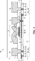
図1は、装置の概略断面図を示す。電子装置10は、第1の面41と第2の面42を有するシリコンの基板1を含む。第2の面42上では、基板1は、シリコン酸化膜の電気絶縁層2で覆われる。第1のキャパシタ11の第1のキャパシタ電極21が画定されるアルミニウムの第1の電気導電層3は層2上に存在する。ビア13の領域で除去される誘電材料5の層は、第1の電気導電層3上に位置する。誘電材料5の層は、0.5≦x≦2のSiNxを含み、キャパシタ11の中間区域24の誘電体26を構成する。エッジ区域22及び23では、誘電体26は、誘電材料5の層だけでなく、電気絶縁材料5の層、この例では1≦x≦2のSiOxも含む。アルミニウムを含む中間層6は誘電材料5の層上に位置し、電気絶縁材料4の層に部分的に覆われる。導電トラック28は中間層6中に画定される。アルミニウムも含む第2の電気導電層7の第2のパターン29は、この導電トラック28に対する電気コンタクト中にある。導電トラック28及び第2のパターン29は共に、第1のキャパシタ11の第2のキャパシタ電極25を形成する。第2の導電層7は、さらに、第1のパターンとしての第1のコイル12、ビア13及び相互接続14を含み、保護層8に覆われる。中間層6上の第2のパターン29の垂直射影は、導電トラック28の外側に部分的に位置する。第1の導電層3上の第2のパターン29の垂直射影は、第1のキャパシタ電極21の外側、すなわち、相互接続14の領域に部分的に位置する。この相互接続14は、第2のキャパシタ電極25を装置110の他の部分と接続するために必要である。従って、第1の導電層3上の第2のキャパシタ電極25の垂直射影は、第1のキャパシタ電極21の内部に少なくとも部分的に位置する。
FIG. 1 shows a schematic cross-sectional view of the device. The
本発明によれば、装置10は、第1の横型PINダイオード50と第2の横型PINダイオード60を含む。PINダイオード50、60の両方は、この実施例では、第2のp導電型領域52、62内に横方向に位置する第1のn導電型領域51、61と一体となった円形形状を有する。n導電型領域51、61とp導電型領域52、62との間に真性領域53、63が設けられる。本発明によれば、第1のPINダイオード50の真性領域53の幅d1は、第2のPINダイオードの真性領域63の幅d2より小さい。この結果、第1のPINダイオード50は、第2のPINダイオード60より低い抵抗を有する。従って、第1のPINダイオード50は、携帯電話の送信パスにおける集積に極めて適切しており、第2のPINダイオード60は、携帯電話の受信パスにおける集積に適している。クロストークを防ぐために、適切な高抵抗である基板1は、クロストークを防ぐ手段を含む。冒頭の測定が示したように、8μmの幅を有する真性領域の横型PINダイオードは、1mAの電流と100MHzの周波数で3〜6Ωの抵抗を有し、抵抗は、電流が増加すると、10mAで0.3〜0.6Ωまで減少する。挿入損失は700MHz周辺の周波数で−1.5dBより小さく、低電流でもある。絶縁破壊電圧は20V〜30Vである。
In accordance with the present invention, the
図1から明らかなように、横型PINダイオード50、60は、上部から接触され得るという明らかな利点を有する。相互接続56、66、67は、このように、第1及び第2の導電層3、7に集積され得る。当業者に明らかなように、PINダイオードは相互接続を介して回路に集積され得る。ここでの実施例は、例えば、ここでの記述を含む未公開出願EP03102255.1(PHNL030882)及びEP02079324.6(PHNL020986)から知られている。インダクタ12とキャパシタ11がPINダイオード50、60の間に横方向に存在するような、示された実際の配置が唯一典型的である。他の配置も同様に設計されても良い。ここでの例は、インダクタとPINダイオードが横方向に間隔をあけて分離され、インダクタ及びキャパシタの直接の近傍の下又は内部の基板領域だけが高抵抗で作られる。さらに、第2の導電層7は、大きな厚さを有するように示される。しかしながら、銅のような代替的な材料を選択することにより、この厚さは低減され得る。
As is apparent from FIG. 1, the
図2は、アンテナスイッチに利用するためのPINダイオードを有する回路を図示する電気的概略図を示す。示されたものは、1周波数帯のみの回路である。回路は、電力増幅器を有する送信パスに対する接続点110、低雑音増幅器を有する受信パスに対する接続点120、そして、アンテナ130に対する接続点を含む。さらに、受信パス120に対する接続点とアースとの間に配置される第1のPINダイオード50、及び、送信パス110とアンテナ130に対する接続点との間に配置される第2のPINダイオードと同様に、4分の1波長λ/4に共鳴する送信線140が設けられる。送信パス110からの信号がアンテナ130に送られなければならない場合は、PINダイオード50、60はスイッチが入る。代替的には、受信モードでは、PINダイオード50、60はスイッチが切れる。
FIG. 2 shows an electrical schematic diagram illustrating a circuit having a PIN diode for use in an antenna switch. What is shown is a circuit for only one frequency band. The circuit includes a
図3は、基板における電気的損失のモデルである電気的概略図を示す。このモデルからは、キャパシタにとっては、基板損失が低周波数で支配的であり、インダクタにとっては、損失が高周波数で支配的になり始めるということが分かる。損失誘導基板は、損失誘導バルクとSi−SiO2インタフェースで誘導される損失とに分割され得る。ゼロバイアス条件下では、集積層が、例えば、一般的に熱シリコン酸化膜に存在する固定電荷により誘導されるSi−SiO2インタフェースに存在する。CV測定によれば、蓄積された電荷の量は、おおよそ、全ての移動電荷が4kΩmシリコンのバルクに存在するよりも大きな規模であると推定される。従って、バルク抵抗に隣接して、この集積された電荷に関連するインタフェース抵抗が、上部に加工された受動損失に大いに影響を与える。シリコン基板のアモルファスの上面を作ることによりSi−SiO2インタフェースでの低抵抗が増加させられ得るし、その結果、キャリア移動度が減少する。我々の場合は、このことは、熱酸化膜の成長後で第1の導電層3の堆積前に、例えば、アルゴン又は窒素のイオン注入を用いて達成される。 FIG. 3 shows an electrical schematic that is a model of electrical losses in the substrate. From this model, it can be seen that for capacitors, substrate losses are dominant at low frequencies, and for inductors, losses begin to dominate at high frequencies. Loss inducing substrate may be divided into loss and induced losses induced bulk and Si-SiO 2 interface. At zero bias conditions, accumulation layer, for example, generally present in the Si-SiO 2 interface induced by fixed charges existing in thermal silicon oxide film. According to CV measurements, the amount of stored charge is estimated to be approximately larger than all the mobile charge is present in the bulk of 4 kΩm silicon. Thus, adjacent to the bulk resistor, the interface resistance associated with this integrated charge greatly affects the passive loss fabricated on top. It resistance in Si-SiO 2 interface can be increased by making the upper surface of the amorphous silicon substrate, as a result, carrier mobility is reduced. In our case, this is achieved by using, for example, argon or nitrogen ion implantation after the growth of the thermal oxide and before the deposition of the first conductive layer 3.
図4は、基板抵抗の関数としての5nHインダクタのQ計数のグラフを示す。インダクタのQの重要な改善は、本発明で用いられる高抵抗シリコン(ρ−4kΩ..cm)で得られることが分かった。インダクタのQの増加は、ほとんどが1kΩ.cm未満のバルク抵抗の欠如である。1kΩmより低い基板抵抗に関しては、バルク誘導損失がSi−SiO2インタフェースで誘導される損失を明らかに支配する。 FIG. 4 shows a graph of the Q count of a 5 nH inductor as a function of substrate resistance. It has been found that significant improvements in inductor Q can be obtained with high resistance silicon (ρ-4 kΩ... Cm) used in the present invention. The increase in the Q of the inductor is almost 1 kΩ. Lack of bulk resistance below cm. For substrate resistances below 1 kΩm, bulk induced losses clearly dominate the losses induced at the Si—SiO 2 interface.
基板損失のさらなる抑制は、バルクへの格子欠陥の導入により達成される。シリコンのバンドギャップ内の局部的なエネルギー状態を作ることにより、移動電荷はトラップされなくなり、結果として、固有の抵抗が増加する。結晶格子に対する永続的なダメージは、電磁放射線の高エネルギー(E>1MeV)ビーム、又はイオンのような粒子及び中性子を用いた場合に引き起こされても良い。放射は低温プロセスであるので、層3、4、5、7の積層が堆積させられ、構造化された後に行われ得る。ファン・デ・グラーフ(Van−de−Graaf)アクセラレータは、150MeVの電子エネルギーを作り出すために用いられる。処理されたウェハは、1.4×10¹⁵e.cm―2のドーズ量で放射される。
Further suppression of substrate loss is achieved by introducing lattice defects into the bulk. By creating a local energy state within the silicon bandgap, the mobile charge is not trapped, resulting in an increase in intrinsic resistance. Permanent damage to the crystal lattice may be caused when using high energy (E> 1 MeV) beams of electromagnetic radiation, or particles such as ions and neutrons. Since radiation is a low temperature process, it can be done after the stack of
図5は、異なる取り扱いを受けた基板に対する周波数の関数としてのキャパシタ11の等価直列抵抗(ESR)のグラフを示す。破線(dotted line)は、取り扱いを受けていない装置を示し、点線(dashed line)は、放射を伴う取り扱いを受けた装置を示す。破線と点線(dash−and−dot line)は、注入を伴う取り扱いを受けた装置を示す。破点線(dash−dot line)は、注入と照射の両方を伴う取り扱いを受けた装置を示す。比較のために、ESRは、実践で示されるように、ガラス基板上で処理された同じキャパシタのものがプロットされる。この図5によれば、電子ビーム放射後のESRが、インタフェースへのイオン注入を用いて達成されるのとほぼ同程度だけ低減したことが分かった。ESRは、インタフェースへのイオン注入を伴う電子ビーム放射と組み合わせる場合に、さらに低くなる。期待されるように、このことは、放射が注入に対して相補的であることを明らかに示す。図3に図示されたモデルにこれらのデータをフィルタリングすることは、効果的な基板抵抗が、「取り扱われていない」高抵抗シリコンと比較して、要素10,000(!)程も増加することを示す。電子ビーム放射の後、キャパシタ11のリーク電流はそれほど変化しなかった。
FIG. 5 shows a graph of the equivalent series resistance (ESR) of
Claims (11)
第1及び第2の横型PINダイオードは前記基板に画定され、前記PINダイオードが互いにp導電型領域、n導電型領域、及び中間真性領域を有し、前記PINダイオードのうち前記第1のPINダイオードの前記真性領域の幅は前記第2のPINダイオードの真性領域の幅よりも大きく、前記インダクタと前記キャパシタは2つのPINダイオード間に横方向に存在し、前記第1のPINダイオードは受信パス用ダイオードを構成し、前記第2のPINダイオードは送信パス用ダイオードを構成する、電子装置。A network of at least one thin film capacitor and at least one inductor on a first surface of a substrate of semiconductor material, the substrate having a high resistance of 100 Ω · cm or more to limit electrical loss of the inductor Comprising an electrically insulating surface layer on the first surface;
First and second lateral PIN diodes are defined in the substrate, and the PIN diodes have a p-conductivity type region, an n-conductivity type region, and an intermediate intrinsic region, and the first PIN diode of the PIN diodes The width of the intrinsic region of the second PIN diode is larger than the width of the intrinsic region of the second PIN diode, the inductor and the capacitor are present laterally between two PIN diodes, and the first PIN diode is used for a reception path. An electronic device comprising a diode, wherein the second PIN diode comprises a transmission path diode .
Applications Claiming Priority (3)
| Application Number | Priority Date | Filing Date | Title |
|---|---|---|---|
| EP04101966 | 2004-05-06 | ||
| EP04101966.2 | 2004-05-06 | ||
| PCT/IB2005/051433 WO2005109636A1 (en) | 2004-05-06 | 2005-05-03 | Electronic device |
Publications (2)
| Publication Number | Publication Date |
|---|---|
| JP2007536759A JP2007536759A (en) | 2007-12-13 |
| JP5026257B2 true JP5026257B2 (en) | 2012-09-12 |
Family
ID=34965733
Family Applications (1)
| Application Number | Title | Priority Date | Filing Date |
|---|---|---|---|
| JP2007512641A Expired - Fee Related JP5026257B2 (en) | 2004-05-06 | 2005-05-03 | Electronic equipment |
Country Status (7)
| Country | Link |
|---|---|
| US (1) | US8901703B2 (en) |
| EP (1) | EP1745545B1 (en) |
| JP (1) | JP5026257B2 (en) |
| CN (1) | CN100533967C (en) |
| AT (1) | ATE388520T1 (en) |
| DE (1) | DE602005005189T2 (en) |
| WO (1) | WO2005109636A1 (en) |
Families Citing this family (8)
| Publication number | Priority date | Publication date | Assignee | Title |
|---|---|---|---|---|
| EP2024990B1 (en) * | 2006-05-18 | 2011-06-29 | Ipdia | Method of increasing the quality factor of an inductor in a semiconductor device |
| KR100747657B1 (en) | 2006-10-26 | 2007-08-08 | 삼성전자주식회사 | Semiconductor devices capable of macro and micro frequency tuning, and antennas and frequency tuning circuits having them |
| JP5399513B2 (en) * | 2008-12-31 | 2014-01-29 | シエラ・ネバダ・コーポレイション | Monolithic semiconductor microwave switch array |
| US8237243B2 (en) | 2009-03-18 | 2012-08-07 | International Business Machines Corporation | On-chip capacitors with a variable capacitance for a radiofrequency integrated circuit |
| JP5481127B2 (en) * | 2009-08-19 | 2014-04-23 | 株式会社ジャパンディスプレイ | SENSOR ELEMENT AND ITS DRIVING METHOD, SENSOR DEVICE, DISPLAY DEVICE WITH INPUT FUNCTION, AND ELECTRONIC DEVICE |
| JP6425633B2 (en) * | 2015-08-21 | 2018-11-21 | 住重アテックス株式会社 | Semiconductor device and method of manufacturing semiconductor device |
| US12569639B2 (en) | 2020-01-21 | 2026-03-10 | Wearair Ventures, Inc. | Efficient enriched oxygen airflow systems and methods |
| US20210220599A1 (en) | 2020-01-21 | 2021-07-22 | Wearair Ventures, Inc. | Efficient enriched oxygen airflow systems and methods |
Family Cites Families (27)
| Publication number | Priority date | Publication date | Assignee | Title |
|---|---|---|---|---|
| US4474623A (en) * | 1982-04-26 | 1984-10-02 | Raytheon Company | Method of passivating a semiconductor body |
| US4810980A (en) * | 1987-06-04 | 1989-03-07 | Texas Instruments, Inc. | Matched variable attenuation switched limiter |
| US5280194A (en) * | 1988-11-21 | 1994-01-18 | Micro Technology Partners | Electrical apparatus with a metallic layer coupled to a lower region of a substrate and metallic layer coupled to a lower region of a semiconductor device |
| GB2228616B (en) | 1989-02-22 | 1992-11-04 | Stc Plc | Opto-electronic device |
| JP3120938B2 (en) * | 1994-02-16 | 2000-12-25 | 松下電子工業株式会社 | Semiconductor integrated device and method of manufacturing the same |
| JP3959125B2 (en) | 1994-09-14 | 2007-08-15 | 株式会社東芝 | Semiconductor device |
| DE19533206A1 (en) | 1995-09-08 | 1997-03-13 | Daimler Benz Ag | Planar PIN diode and process for its manufacture |
| JPH09214278A (en) * | 1996-01-30 | 1997-08-15 | Nec Corp | Pin diode variable attenuator |
| TW392392B (en) | 1997-04-03 | 2000-06-01 | Lucent Technologies Inc | High frequency apparatus including a low loss substrate |
| US5986517A (en) | 1998-01-06 | 1999-11-16 | Trw Inc. | Low-loss air suspended radially combined patch for N-way RF switch |
| JP3309959B2 (en) | 1998-04-16 | 2002-07-29 | 日本電気株式会社 | Semiconductor device |
| DE19821726C1 (en) * | 1998-05-14 | 1999-09-09 | Texas Instruments Deutschland | Integrated CMOS circuit for high frequency applications, e.g. as a symmetrical mixer input stage or an impedance transformer |
| KR100697405B1 (en) | 2000-02-15 | 2007-03-20 | 코닌클리즈케 필립스 일렉트로닉스 엔.브이. | Electronic devices |
| EP1137055A1 (en) | 2000-03-24 | 2001-09-26 | Infineon Technologies AG | Method for manufacturing a high-frequency semiconductor structure and high-frequency semiconductor structure |
| JP2001352079A (en) | 2000-06-07 | 2001-12-21 | Nec Corp | Diode and method of manufacturing the same |
| DE60140722D1 (en) | 2000-09-05 | 2010-01-21 | Nxp Bv | Integrated electromagnetic shielding device |
| US6660616B2 (en) * | 2001-01-31 | 2003-12-09 | Texas Instruments Incorporated | P-i-n transit time silicon-on-insulator device |
| DE10127952A1 (en) * | 2001-06-08 | 2002-12-19 | Infineon Technologies Ag | Lateral PIN diode and method of making the same |
| JP4299488B2 (en) | 2001-12-07 | 2009-07-22 | 太陽誘電株式会社 | High frequency module and manufacturing method thereof |
| US6620673B1 (en) * | 2002-03-08 | 2003-09-16 | Alpine Microsystems, Inc. | Thin film capacitor having multi-layer dielectric film including silicon dioxide and tantalum pentoxide |
| JP2004014658A (en) | 2002-06-05 | 2004-01-15 | Renesas Technology Corp | Semiconductor device and manufacturing method therefor |
| JP4004357B2 (en) | 2002-08-29 | 2007-11-07 | 新電元工業株式会社 | diode |
| WO2004036778A1 (en) | 2002-10-14 | 2004-04-29 | Koninklijke Philips Electronics N.V. | Transmit and receive antenna switch |
| US7132723B2 (en) * | 2002-11-14 | 2006-11-07 | Raytheon Company | Micro electro-mechanical system device with piezoelectric thin film actuator |
| WO2005008908A1 (en) | 2003-07-22 | 2005-01-27 | Koninklijke Philips Electronics N.V. | Antenna switch with adaptive filter |
| JP2007231072A (en) | 2006-02-28 | 2007-09-13 | Three M Innovative Properties Co | Coating composition and article using the same |
| JP2009214278A (en) | 2008-03-13 | 2009-09-24 | Nikon Corp | Grinding wheel |
-
2005
- 2005-05-03 US US11/579,679 patent/US8901703B2/en not_active Expired - Lifetime
- 2005-05-03 WO PCT/IB2005/051433 patent/WO2005109636A1/en not_active Ceased
- 2005-05-03 DE DE602005005189T patent/DE602005005189T2/en not_active Expired - Lifetime
- 2005-05-03 EP EP05732041A patent/EP1745545B1/en not_active Expired - Lifetime
- 2005-05-03 JP JP2007512641A patent/JP5026257B2/en not_active Expired - Fee Related
- 2005-05-03 CN CNB2005800141916A patent/CN100533967C/en not_active Expired - Fee Related
- 2005-05-03 AT AT05732041T patent/ATE388520T1/en not_active IP Right Cessation
Also Published As
| Publication number | Publication date |
|---|---|
| ATE388520T1 (en) | 2008-03-15 |
| EP1745545B1 (en) | 2008-03-05 |
| US20070228514A1 (en) | 2007-10-04 |
| US8901703B2 (en) | 2014-12-02 |
| JP2007536759A (en) | 2007-12-13 |
| WO2005109636A1 (en) | 2005-11-17 |
| EP1745545A1 (en) | 2007-01-24 |
| DE602005005189T2 (en) | 2009-03-19 |
| CN100533967C (en) | 2009-08-26 |
| DE602005005189D1 (en) | 2008-04-17 |
| CN1951004A (en) | 2007-04-18 |
Similar Documents
| Publication | Publication Date | Title |
|---|---|---|
| US8058689B2 (en) | Techniques to reduce substrate cross talk on mixed signal and RF circuit design | |
| KR100522655B1 (en) | High q inductor with faraday shield and dielectric well buried in substrate | |
| KR101831219B1 (en) | Method of manufacturing vertical pin diodes | |
| US6310387B1 (en) | Integrated circuit inductor with high self-resonance frequency | |
| US20090039457A1 (en) | Low crosstalk substrate for mixed-signal integrated circuits | |
| US6258688B1 (en) | Method to form a high Q inductor | |
| US6448604B1 (en) | Integrated adjustable capacitor | |
| CN101449362B (en) | Method for Improving the Quality Factor of Inductors in Semiconductor Devices | |
| JP2008516441A (en) | Semiconductor device and use thereof | |
| JP5026257B2 (en) | Electronic equipment | |
| US7176546B2 (en) | Diode circuit and method of producing a diode circuit | |
| CN1947250B (en) | Semiconductor device and method of manufacturing such a device | |
| JP2004303744A (en) | Monolithic microwave integrated circuit and its fabrication method | |
| US7902013B1 (en) | Method of forming a semiconductor die with reduced RF attenuation | |
| WO2021242972A1 (en) | Low-loss millimeter wave transmission lines on silicon substrate | |
| US9941353B2 (en) | Structure and method for mitigating substrate parasitics in bulk high resistivity substrate technology |
Legal Events
| Date | Code | Title | Description |
|---|---|---|---|
| A621 | Written request for application examination |
Free format text: JAPANESE INTERMEDIATE CODE: A621 Effective date: 20080502 |
|
| A711 | Notification of change in applicant |
Free format text: JAPANESE INTERMEDIATE CODE: A711 Effective date: 20080626 |
|
| A977 | Report on retrieval |
Free format text: JAPANESE INTERMEDIATE CODE: A971007 Effective date: 20111014 |
|
| A131 | Notification of reasons for refusal |
Free format text: JAPANESE INTERMEDIATE CODE: A131 Effective date: 20111018 |
|
| A521 | Request for written amendment filed |
Free format text: JAPANESE INTERMEDIATE CODE: A523 Effective date: 20120113 |
|
| TRDD | Decision of grant or rejection written | ||
| A01 | Written decision to grant a patent or to grant a registration (utility model) |
Free format text: JAPANESE INTERMEDIATE CODE: A01 Effective date: 20120525 |
|
| A01 | Written decision to grant a patent or to grant a registration (utility model) |
Free format text: JAPANESE INTERMEDIATE CODE: A01 |
|
| A61 | First payment of annual fees (during grant procedure) |
Free format text: JAPANESE INTERMEDIATE CODE: A61 Effective date: 20120620 |
|
| FPAY | Renewal fee payment (event date is renewal date of database) |
Free format text: PAYMENT UNTIL: 20150629 Year of fee payment: 3 |
|
| R150 | Certificate of patent or registration of utility model |
Ref document number: 5026257 Country of ref document: JP Free format text: JAPANESE INTERMEDIATE CODE: R150 |
|
| R250 | Receipt of annual fees |
Free format text: JAPANESE INTERMEDIATE CODE: R250 |
|
| S111 | Request for change of ownership or part of ownership |
Free format text: JAPANESE INTERMEDIATE CODE: R313113 |
|
| R350 | Written notification of registration of transfer |
Free format text: JAPANESE INTERMEDIATE CODE: R350 |
|
| R250 | Receipt of annual fees |
Free format text: JAPANESE INTERMEDIATE CODE: R250 |
|
| R250 | Receipt of annual fees |
Free format text: JAPANESE INTERMEDIATE CODE: R250 |
|
| R250 | Receipt of annual fees |
Free format text: JAPANESE INTERMEDIATE CODE: R250 |
|
| R250 | Receipt of annual fees |
Free format text: JAPANESE INTERMEDIATE CODE: R250 |
|
| R250 | Receipt of annual fees |
Free format text: JAPANESE INTERMEDIATE CODE: R250 |
|
| R250 | Receipt of annual fees |
Free format text: JAPANESE INTERMEDIATE CODE: R250 |
|
| R250 | Receipt of annual fees |
Free format text: JAPANESE INTERMEDIATE CODE: R250 |
|
| LAPS | Cancellation because of no payment of annual fees |