JP2004014658A - Semiconductor device and manufacturing method therefor - Google Patents
Semiconductor device and manufacturing method therefor Download PDFInfo
- Publication number
- JP2004014658A JP2004014658A JP2002163800A JP2002163800A JP2004014658A JP 2004014658 A JP2004014658 A JP 2004014658A JP 2002163800 A JP2002163800 A JP 2002163800A JP 2002163800 A JP2002163800 A JP 2002163800A JP 2004014658 A JP2004014658 A JP 2004014658A
- Authority
- JP
- Japan
- Prior art keywords
- layer
- semiconductor region
- conductivity type
- epitaxial layer
- impurity
- Prior art date
- Legal status (The legal status is an assumption and is not a legal conclusion. Google has not performed a legal analysis and makes no representation as to the accuracy of the status listed.)
- Pending
Links
Images


Abstract
Description
【0001】
【発明の属する技術分野】
本発明は、半導体装置およびその製造技術に関し、特に、PIN(Positive Intrinsic Negative)ダイオードを有する半導体装置に適用して有効な技術に関する。
【0002】
【従来の技術】
たとえばマグロウヒルブック株式会社発行「半導体デバイスの基礎」昭和61年3月25日発行、グローブ著、図6.1にシリコンのプレーナ型n+p接合ダイオードが記載されている。
【0003】
このn+p接合ダイオードは、まず相対的に高濃度(たとえば1019cm−3)にドープされたp型の導電性を示す基板上に、相対的に低濃度(たとえば1016cm−3)にドープされるp型エピタキシャル膜を成長させる。次に、熱酸化処理によりエピタキシャル膜の表面にシリコン酸化膜を形成した後、シリコン酸化膜の一部を取り除いて窓を形成し、続いてその窓を通じてn型の導電性を示す不純物をエピタキシャル膜へ拡散することにより、n+p接合ダイオードが形成される。このような接合は、基板上に同時に複数個形成される。
【0004】
【発明が解決しようとする課題】
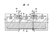
本発明者は、アンテナスイッチ用または位相シフト用のPINダイオードについて検討した。図8は、本発明者によって検討されたPINダイオードの一例を示す半導体基板の要部断面図である。
【0005】
n型の導電性を示す半導体基板(N層)51の表面上にエピタキシャル層(I層)52が形成されており、このエピタキシャル層52に、n型の導電性を示す半導体領域からなるアイソレーション層53に囲まれてp型の導電性を示す半導体領域(P層)54が形成されている。p型の導電性を示す半導体領域54に接して設けられた第1の電極55と、半導体基板51の裏面に接して設けられた第2の電極56との間に、p型の導電性を示す半導体領域(P層)54、エピタキシャル層(I層)52および半導体基板(N層)51からなるPINダイオードが構成される。
【0006】
しかしながら、信号周波数が互いに異なる上記PINダイオードが複数個並列に並んでいる場合、以下の問題が生ずることを本発明者は見いだした。
【0007】
すなわち、入力信号の周波数が互いに異なる第1のPINダイオードE1と第2のPINダイオードE2とを同時にオンさせた場合、エピタキシャル層52に注入されたキャリアはエピタキシャル層52全体に広がるため、第1のPINダイオードE1の高周波信号S1と第2のPINダイオードE2の高周波信号S2とはお互いに干渉(変調)して、出力信号に歪みが生ずることがある。
【0008】
アイソレーション層53を深くすることによって、第1のPINダイオードE1の高周波信号S1と第2のPINダイオードE2の高周波信号S2との間で生ずる干渉(変調)を防ぐことができる。しかしながら、イオン注入法によりエピタキシャル層52に不純物を導入し、その後熱処理を施すことによってアイソレーション層53は形成されるため、その深さには限界があり、エピタキシャル層52が相対的に厚い場合は、アイソレーション層53では上記干渉(変調)を防ぐことが難しいと考えられる。
【0009】
本発明の目的は、複数個並列に並んだPINダイオード間の干渉を軽減することのできる技術を提供することにある。
【0010】
本発明の前記ならびにその他の目的と新規な特徴は、本明細書の記述および添付図面から明らかになるであろう。
【0011】
【課題を解決するための手段】
本願において開示される発明のうち、代表的なものの概要を簡単に説明すれば、次のとおりである。
【0012】
本発明は、基板上にn型の導電性を示す不純物が相対的低濃度に導入されたエピタキシャル層が形成され、エピタキシャル層の上面側に、p型の導電性を示す不純物が相対的高濃度に導入された第1の半導体領域と、第1の半導体領域の周辺に所定の距離をおいて、n型の導電性を示す不純物が相対的高濃度に導入された第2の半導体領域とが形成されており、第1の半導体領域、エピタキシャル層および第2の半導体領域からなるダイオードが構成されるものである。
【0013】
本発明は、基板上にn型の導電性を示す不純物が相対的低濃度に導入されたエピタキシャル層を形成する工程と、エピタキシャル層上に第1の絶縁膜を形成する工程と、第1の絶縁膜の一部を除去した後、第1の絶縁膜を除去した領域を通してp型の導電性を示す不純物をエピタキシャル層へ導入して、相対的高濃度の第1の半導体領域を形成する工程と、第1の絶縁膜の上層に第2の絶縁膜を形成する工程と、第1の半導体領域から所定の距離をおいて、所定の幅で第1の半導体領域周辺の第1および第2の絶縁膜を除去した後、第1および第2の絶縁膜を除去した領域を通してn型の導電性を示す不純物をエピタキシャル層へ導入して、相対的高濃度の第2の半導体領域を形成する工程とを有するものである。
【0014】
【発明の実施の形態】
以下、本発明の実施の形態を図面に基づいて詳細に説明する。なお、実施の形態を説明するための全図において、同一の機能を有する部材には同一の符号を付し、その繰り返しの説明は省略する。
【0015】
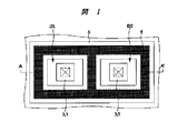
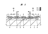
図1は、本発明の一実施の形態であるPINダイオードを示す半導体基板の要部平面図、図2は、図1のA−A′線におけるPINダイオードを示す半導体基板の要部断面図である。なお、図には、並列に並んだ2つのPINダイオードを記載したが、基板上に3つ以上のPINダイオードを配置してもよい。また、図1中、網掛けのハッチングで示す領域は、PINダイオードの一部を構成するN層を示す。
【0016】
シリコン単結晶からなる半導体基板1の上層に、n型の導電性を示す10μm程度の厚さのエピタキシャル層(以下、I層と記す)2が形成されている。I層2には、一辺が50〜150μm程度の矩形からなるp型の導電性を示す半導体領域(以下、P層と記す)3が形成されており、その周辺に所定の距離をおいて、50〜150μm程度の幅を有し、n型の導電性を示す半導体領域(以下、N層と記す)4が形成されている。隣接するP層3は、200〜400μm程度の間隔で離れており、P層3の深さは5μm程度である。またN層4の深さは5〜10μm程度であり、N層4は半導体基板1と接してもよい。
【0017】
さらにアノード、カソードの両電極がI層2の上面側に形成されており、第1の電極(アノード電極)5がP層3に、第2の電極(カソード電極)6がN層4に接している。従って、I層2の上面側に設けられた第1の電極5と第2の電極6との間に、P層3、I層2およびN層4からなるPINダイオードD1,D2が構成される。P層3、I層2およびN層4の不純物濃度は、それぞれ1020cm−3、1013cm−3および1020cm−3程度とすることができる。なお、第1の電極5とI層2または第2の電極6とI層2とが接触しないように、I層2の上層には2μm程度の厚さの絶縁膜7が形成されている。
【0018】
このように、本実施の形態によれば、PINダイオードD1,D2を構成するP層3およびN層4をI層2の上面側に配置して、N層4とP層3とを閉回路とし、N層4に電位、たとえば0.7Vを与えることにより、N層4をキャリア(電子)の注入源とすることができる。従ってキャリアをI層2の表面近傍に集めることができ、さらにN層4を半導体基板1に到達させた場合は、キャリアを各PINダイオードD1,D2が形成されたI層2に納めることができる。その結果、PINダイオードD1,D2が同時にオンしても、I層2全体へのキャリアの広がりを防ぐことができるので、PINダイオードD1の高周波信号S1とPINダイオードD2の高周波信号S2とがお互いに干渉するのを防ぐことができる。これにより、PINダイオードD1,D2を搭載した半導体装置の出力信号の歪み、チャンネル間妨害、混変調などの不具合を改善することができる。
【0019】
また、P層3とN層4との距離によってダイオード特性は制御されるので、ダイオード特性に与えるI層2の厚さの影響が小さくなる。これにより、I層2の厚さを相対的に薄く形成することができて、N層4を半導体基板1に接触させて形成することが容易となる。
【0020】
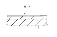
次に、本発明の一実施の形態であるPINダイオードの製造方法を図3〜図7に示す半導体基板の要部断面図を用いて工程順に説明する。
【0021】
まず、図3に示すように、たとえばn型のシリコン単結晶からなる半導体基板(円形の薄い板状に加工した半導体ウエハ)1を用意する。次に、半導体基板1の表面にエピタキシャル法により、n型のシリコン単結晶膜を成長させて、不純物濃度1013cm−3程度、厚さ10μm程度のI層2を形成する。次に、熱酸化処理を施して、I層2の表面に厚さ1μm程度のシリコン酸化膜7aを形成する。
【0022】
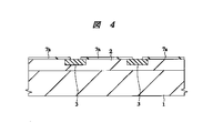
次に、図4に示すように、レジストパターンをマスクとしたドライエッチングにより、シリコン酸化膜7aの一部に200〜400μm程度の間隔で、たとえば矩形の穴を開口した後、たとえばp型の不純物をI層2にイオン注入し、続いて熱処理を施すことによって、不純物濃度1020cm−3程度、深さ5μm程度のP層3を形成する。P層3の一辺は50〜150μm程度の矩形とすることができる。
【0023】
次に、図5に示すように、シリコン酸化膜7aの上層に厚さ1μm程度のシリコン酸化膜7bを、たとえばCVD(Chemical Vapor Deposition)法で堆積する。
【0024】
次に、図6に示すように、レジストパターンをマスクとしたドライエッチングにより、P層3から所定の距離をおいて、50〜150μm程度の幅でP層3の周辺のシリコン酸化膜7a,7bを除去する。続いて、n型の不純物をI層2にイオン注入し、続いて熱処理を施すことによって、不純物濃度1020cm−3程度、深さ5〜10μm程度のN層4を形成する。
【0025】
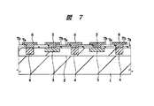
次に、図7に示すように、P層3の上方のシリコン酸化膜7bを除去した後、シリコン酸化膜7bの上層に金属膜、たとえばアルミニウム合金膜を堆積する。この後、レジストパターンをマスクとしたドライエッチングにより、この金属膜を加工して、P層3に接続する第1の電極5およびN層4に接続する第2の電極6を形成する。これにより、PINダイオードが略完成する。
【0026】
以上、本発明者によってなされた発明を発明の実施の形態に基づき具体的に説明したが、本発明は前記実施の形態に限定されるものではなく、その要旨を逸脱しない範囲で種々変更可能であることは言うまでもない。
【0027】
たとえば、前記実施の形態では、PINダイオードに適用した場合について説明したが、他のダイオード、たとえばバリキャップダイオード、またはチェナーダイオード、スイッチングダイオード、ショットキーダイオードなどのpn接合ダイオードにも適用することができて、同様の効果が得られる。
【0028】
【発明の効果】
本願において開示される発明のうち、代表的なものによって得られる効果を簡単に説明すれば以下のとおりである。
【0029】
PINダイオードを構成するP層およびN層をI層の上面側に配置し、N層に電位を与えてN層をカソードとして用いることにより、キャリアをI層の表面近傍に集めることができる。これにより、複数のPINダイオードが同時にオンしても、I層全体へのキャリアの広がりを防ぐことができるので、複数のPINダイオード間において高周波信号がお互いに干渉するのを防止することができる。
【図面の簡単な説明】
【図1】本発明の一実施の形態であるPINダイオードを示す半導体基板の要部平面図である。
【図2】図1のA−A′線におけるPINダイオードを示す半導体基板の要部断面図である。
【図3】本発明の一実施の形態であるPINダイオードの製造方法を示す半導体基板の要部断面図である。
【図4】本発明の一実施の形態であるPINダイオードの製造方法を示す半導体基板の要部断面図である。
【図5】本発明の一実施の形態であるPINダイオードの製造方法を示す半導体基板の要部断面図である。
【図6】本発明の一実施の形態であるPINダイオードの製造方法を示す半導体基板の要部断面図である。
【図7】本発明の一実施の形態であるPINダイオードの製造方法を示す半導体基板の要部断面図である。
【図8】本発明が検討したPINダイオードを示す半導体基板の要部断面図である。
【符号の説明】
1 半導体基板
2 エピタキシャル層(I層)
3 p型の導電性を示す半導体領域(P層)
4 n型の導電性を示す半導体領域(N層)
5 第1の電極
6 第2の電極
7 絶縁膜
7a シリコン酸化膜
7b シリコン酸化膜
51 半導体基板(N層)
52 エピタキシャル層(I層)
53 アイソレーション層
54 p型の導電性を示す半導体領域(P層)
55 第1の電極
56 第2の電極
D1 PINダイオード
D2 PINダイオード
S1 高周波信号
S2 高周波信号
E1 第1のPINダイオード
E2 第2のPINダイオード[0001]
TECHNICAL FIELD OF THE INVENTION
The present invention relates to a semiconductor device and a manufacturing technique thereof, and more particularly to a technique effective when applied to a semiconductor device having a PIN (Positive Intrinsic Negative) diode.
[0002]
[Prior art]
For example, FIG. 6.1, "Basics of Semiconductor Devices", published by McGraw-Hill Book Co., Ltd., issued on Mar. 25, 1986, describes a planar n + p junction diode made of silicon.
[0003]
The n + p junction diode is first formed on a relatively heavily doped (eg, 10 19 cm −3 ) doped p-type conductive substrate on a relatively lightly doped (eg, 10 16 cm −3 ) substrate. Is grown. Next, after forming a silicon oxide film on the surface of the epitaxial film by thermal oxidation treatment, a part of the silicon oxide film is removed to form a window, and then an impurity exhibiting n-type conductivity is formed through the window. By diffusion to form an n + p junction diode. A plurality of such bondings are simultaneously formed on the substrate.
[0004]
[Problems to be solved by the invention]
The present inventors have studied a PIN diode for an antenna switch or a phase shift. FIG. 8 is a sectional view of a principal part of a semiconductor substrate showing an example of a PIN diode studied by the present inventors.
[0005]
An epitaxial layer (I layer) 52 is formed on the surface of a semiconductor substrate (N layer) 51 having n-type conductivity, and the epitaxial layer 52 has an isolation made of a semiconductor region having n-type conductivity. A semiconductor region (P layer) 54 having p-type conductivity and surrounded by the
[0006]
However, the present inventor has found that the following problem occurs when a plurality of PIN diodes having different signal frequencies are arranged in parallel.
[0007]
That is, when the first PIN diode E1 and the second PIN diode E2 having different frequencies of the input signal are simultaneously turned on, the carriers injected into the epitaxial layer 52 spread over the entire epitaxial layer 52. The high-frequency signal S1 of the PIN diode E1 and the high-frequency signal S2 of the second PIN diode E2 may interfere with each other (modulate), causing distortion in the output signal.
[0008]
By increasing the depth of the
[0009]
An object of the present invention is to provide a technique capable of reducing interference between a plurality of PIN diodes arranged in parallel.
[0010]
The above and other objects and novel features of the present invention will become apparent from the description of the present specification and the accompanying drawings.
[0011]
[Means for Solving the Problems]
The following is a brief description of an outline of typical inventions disclosed in the present application.
[0012]
According to the present invention, an epitaxial layer in which an impurity having n-type conductivity is introduced at a relatively low concentration is formed on a substrate, and an impurity having p-type conductivity has a relatively high concentration on an upper surface side of the epitaxial layer. And a second semiconductor region into which impurities having n-type conductivity are introduced at a relatively high concentration at a predetermined distance from the periphery of the first semiconductor region. The first semiconductor region, the epitaxial layer, and the second semiconductor region constitute a diode.
[0013]
The present invention includes a step of forming an epitaxial layer in which an impurity exhibiting n-type conductivity is introduced at a relatively low concentration on a substrate; a step of forming a first insulating film on the epitaxial layer; Forming a relatively high-concentration first semiconductor region by introducing a p-type conductive impurity into the epitaxial layer through the region from which the first insulating film is removed after removing a part of the insulating film; Forming a second insulating film on the first insulating film; and forming a first and second portions around the first semiconductor region with a predetermined width at a predetermined distance from the first semiconductor region. After removing the insulating film, an impurity exhibiting n-type conductivity is introduced into the epitaxial layer through the region from which the first and second insulating films have been removed to form a second semiconductor region having a relatively high concentration. And a process.
[0014]
BEST MODE FOR CARRYING OUT THE INVENTION
Hereinafter, embodiments of the present invention will be described in detail with reference to the drawings. In all the drawings for describing the embodiments, members having the same functions are denoted by the same reference numerals, and repeated description thereof will be omitted.
[0015]
FIG. 1 is a plan view of a principal part of a semiconductor substrate showing a PIN diode according to an embodiment of the present invention, and FIG. 2 is a sectional view of a principal part of the semiconductor substrate showing a PIN diode along line AA 'in FIG. is there. Although two PIN diodes arranged in parallel are shown in the figure, three or more PIN diodes may be arranged on the substrate. In FIG. 1, a hatched region indicates an N layer that constitutes a part of the PIN diode.
[0016]
An epitaxial layer (hereinafter, referred to as an I layer) 2 having a thickness of about 10 μm and exhibiting n-type conductivity is formed on an upper layer of a
[0017]
Further, both anode and cathode electrodes are formed on the upper surface side of the
[0018]
As described above, according to the present embodiment,
[0019]
Further, since the diode characteristics are controlled by the distance between the
[0020]
Next, a method for manufacturing a PIN diode according to an embodiment of the present invention will be described in the order of steps with reference to the cross-sectional views of main parts of a semiconductor substrate shown in FIGS.
[0021]
First, as shown in FIG. 3, a semiconductor substrate (semiconductor wafer processed into a thin circular plate) 1 made of, for example, an n-type silicon single crystal is prepared. Next, an n-type silicon single crystal film is grown on the surface of the
[0022]
Next, as shown in FIG. 4, after a rectangular hole is opened in a part of the
[0023]
Next, as shown in FIG. 5, a
[0024]
Next, as shown in FIG. 6, the
[0025]
Next, as shown in FIG. 7, after removing the
[0026]
As described above, the invention made by the inventor has been specifically described based on the embodiment of the invention. However, the invention is not limited to the embodiment, and can be variously modified without departing from the gist of the invention. Needless to say, there is.
[0027]
For example, in the above embodiment, the case where the present invention is applied to a PIN diode has been described. A similar effect can be obtained.
[0028]
【The invention's effect】
The effects obtained by typical aspects of the invention disclosed in the present application will be briefly described as follows.
[0029]
By arranging the P layer and the N layer constituting the PIN diode on the upper surface side of the I layer and applying a potential to the N layer to use the N layer as a cathode, carriers can be collected near the surface of the I layer. Accordingly, even if a plurality of PIN diodes are turned on at the same time, the spread of carriers to the entire I layer can be prevented, so that high-frequency signals can be prevented from interfering with each other between the plurality of PIN diodes.
[Brief description of the drawings]
FIG. 1 is a plan view of a principal part of a semiconductor substrate showing a PIN diode according to an embodiment of the present invention.
FIG. 2 is a cross-sectional view of a principal part of the semiconductor substrate showing a PIN diode taken along the line AA ′ of FIG. 1;
FIG. 3 is a fragmentary cross-sectional view of the semiconductor substrate, illustrating the method for manufacturing the PIN diode according to one embodiment of the present invention;
FIG. 4 is a fragmentary cross-sectional view of the semiconductor substrate, illustrating the method for manufacturing the PIN diode according to one embodiment of the present invention;
FIG. 5 is a fragmentary cross-sectional view of the semiconductor substrate, illustrating the method for manufacturing the PIN diode according to one embodiment of the present invention;
FIG. 6 is a fragmentary cross-sectional view of the semiconductor substrate, illustrating the method for manufacturing the PIN diode according to one embodiment of the present invention;
FIG. 7 is a fragmentary cross-sectional view of the semiconductor substrate, illustrating the method for manufacturing the PIN diode according to one embodiment of the present invention;
FIG. 8 is a sectional view of a principal part of a semiconductor substrate showing a PIN diode studied by the present invention.
[Explanation of symbols]
3 Semiconductor region showing p-type conductivity (P layer)
4 Semiconductor region showing n-type conductivity (N layer)
5 First electrode 6
52 Epitaxial layer (I layer)
53
55 first electrode 56 second electrode D1 PIN diode D2 PIN diode S1 high frequency signal S2 high frequency signal E1 first PIN diode E2 second PIN diode
Claims (5)
前記第1の半導体領域、前記エピタキシャル層および前記第2の半導体領域からなるダイオードが構成されることを特徴とする半導体装置。An epitaxial layer in which an impurity having a first conductivity type is introduced at a relatively low concentration is formed on a substrate, and an impurity having a second conductivity type different from the first conductivity type is formed on an upper surface of the epitaxial layer. The first conductivity type is introduced at a relatively high concentration, and the impurity having the first conductivity type is introduced at a relatively high concentration at a predetermined distance around the first semiconductor region and the periphery of the first semiconductor region. A second semiconductor region is formed,
A semiconductor device comprising: a diode including the first semiconductor region, the epitaxial layer, and the second semiconductor region.
前記第1の半導体領域、前記エピタキシャル層および前記第2の半導体領域からなるダイオードが構成され、前記第2の半導体領域は前記基板に達していることを特徴とする半導体装置。An epitaxial layer in which an impurity having a first conductivity type is introduced at a relatively low concentration is formed on a substrate, and an impurity having a second conductivity type different from the first conductivity type is formed on an upper surface of the epitaxial layer. The first conductivity type is introduced at a relatively high concentration, and the impurity having the first conductivity type is introduced at a relatively high concentration at a predetermined distance around the first semiconductor region and the periphery of the first semiconductor region. A second semiconductor region is formed,
A semiconductor device comprising a diode comprising the first semiconductor region, the epitaxial layer, and the second semiconductor region, wherein the second semiconductor region reaches the substrate.
前記第1の半導体領域および前記第2の半導体領域からなるダイオードが構成されることを特徴とする半導体装置。A first semiconductor region into which an impurity having a first conductivity type is introduced on an upper surface side of a substrate; and an impurity having a second conductivity type different from the first conductivity type around the first semiconductor region. And a second semiconductor region into which is introduced.
A semiconductor device comprising a diode including the first semiconductor region and the second semiconductor region.
(b)前記エピタキシャル層上に第1の絶縁膜を形成する工程と、
(c)前記第1の絶縁膜の一部を除去した後、前記第1の絶縁膜を除去した領域を通して前記第1の導電型と異なる第2の導電型の不純物を前記エピタキシャル層へ導入して、相対的高濃度の第1の半導体領域を形成する工程と、
(d)前記第1の絶縁膜の上層に第2の絶縁膜を形成する工程と、
(e)前記第1の半導体領域から所定の距離をおいて、所定の幅で前記第1の半導体領域周辺の前記第1および第2の絶縁膜を除去した後、前記第1および第2の絶縁膜を除去した領域を通して前記第1の導電型の不純物を前記エピタキシャル層へ導入して、相対的高濃度の第2の半導体領域を形成する工程とを有することを特徴とする半導体装置の製造方法。(A) forming, on a substrate, an epitaxial layer into which impurities having a first conductivity type are introduced at a relatively low concentration;
(B) forming a first insulating film on the epitaxial layer;
(C) After removing a part of the first insulating film, an impurity of a second conductivity type different from the first conductivity type is introduced into the epitaxial layer through a region where the first insulating film is removed. Forming a relatively high concentration first semiconductor region;
(D) forming a second insulating film on the first insulating film;
(E) at a predetermined distance from the first semiconductor region, removing the first and second insulating films around the first semiconductor region with a predetermined width, and then removing the first and second insulating films. Introducing the impurity of the first conductivity type into the epitaxial layer through a region from which an insulating film has been removed to form a second semiconductor region having a relatively high concentration. Method.
(b)前記エピタキシャル層上に第1の絶縁膜を形成する工程と、
(c)前記第1の絶縁膜の一部を除去した後、前記第1の絶縁膜を除去した領域を通して前記第1の導電型と異なる第2の導電型の不純物を前記エピタキシャル層へ導入して、相対的高濃度の第1の半導体領域を形成する工程と、
(d)前記第1の絶縁膜の上層に第2の絶縁膜を形成する工程と、
(e)前記第1の半導体領域から所定の距離をおいて、所定の幅で前記第1の半導体領域周辺の前記第1および第2の絶縁膜を除去した後、前記第1および第2の絶縁膜を除去した領域を通して前記第1の導電型の不純物を前記エピタキシャル層へ導入して、相対的高濃度の第2の半導体領域を形成する工程とを有し、
前記第2の半導体領域は、前記基板に達することを特徴とする半導体装置の製造方法。(A) forming, on a substrate, an epitaxial layer into which impurities having a first conductivity type are introduced at a relatively low concentration;
(B) forming a first insulating film on the epitaxial layer;
(C) After removing a part of the first insulating film, an impurity of a second conductivity type different from the first conductivity type is introduced into the epitaxial layer through a region where the first insulating film is removed. Forming a relatively high concentration first semiconductor region;
(D) forming a second insulating film on the first insulating film;
(E) at a predetermined distance from the first semiconductor region, removing the first and second insulating films around the first semiconductor region with a predetermined width, and then removing the first and second insulating films. Introducing the impurity of the first conductivity type into the epitaxial layer through the region from which the insulating film has been removed to form a second semiconductor region having a relatively high concentration,
The method of manufacturing a semiconductor device, wherein the second semiconductor region reaches the substrate.
Priority Applications (1)
| Application Number | Priority Date | Filing Date | Title |
|---|---|---|---|
| JP2002163800A JP2004014658A (en) | 2002-06-05 | 2002-06-05 | Semiconductor device and manufacturing method therefor |
Applications Claiming Priority (1)
| Application Number | Priority Date | Filing Date | Title |
|---|---|---|---|
| JP2002163800A JP2004014658A (en) | 2002-06-05 | 2002-06-05 | Semiconductor device and manufacturing method therefor |
Publications (2)
| Publication Number | Publication Date |
|---|---|
| JP2004014658A true JP2004014658A (en) | 2004-01-15 |
| JP2004014658A5 JP2004014658A5 (en) | 2005-07-07 |
Family
ID=30432125
Family Applications (1)
| Application Number | Title | Priority Date | Filing Date |
|---|---|---|---|
| JP2002163800A Pending JP2004014658A (en) | 2002-06-05 | 2002-06-05 | Semiconductor device and manufacturing method therefor |
Country Status (1)
| Country | Link |
|---|---|
| JP (1) | JP2004014658A (en) |
Cited By (4)
| Publication number | Priority date | Publication date | Assignee | Title |
|---|---|---|---|---|
| JP2007536759A (en) * | 2004-05-06 | 2007-12-13 | コーニンクレッカ フィリップス エレクトロニクス エヌ ヴィ | Electronic equipment |
| JP2008113000A (en) * | 2006-10-26 | 2008-05-15 | Samsung Electronics Co Ltd | Semiconductor element capable of tuning macro and micro frequencies, and antenna and frequency tuning circuit including the semiconductor element |
| JP2012514380A (en) * | 2008-12-31 | 2012-06-21 | シエラ・ネバダ・コーポレイション | Monolithic semiconductor microwave switch array |
| JP7436648B2 (en) | 2019-10-24 | 2024-02-21 | 華為技術有限公司 | Semiconductor switch device, its manufacturing method, and solid state phase shifter |
-
2002
- 2002-06-05 JP JP2002163800A patent/JP2004014658A/en active Pending
Cited By (5)
| Publication number | Priority date | Publication date | Assignee | Title |
|---|---|---|---|---|
| JP2007536759A (en) * | 2004-05-06 | 2007-12-13 | コーニンクレッカ フィリップス エレクトロニクス エヌ ヴィ | Electronic equipment |
| US8901703B2 (en) | 2004-05-06 | 2014-12-02 | Nxp, B.V. | Electronic device |
| JP2008113000A (en) * | 2006-10-26 | 2008-05-15 | Samsung Electronics Co Ltd | Semiconductor element capable of tuning macro and micro frequencies, and antenna and frequency tuning circuit including the semiconductor element |
| JP2012514380A (en) * | 2008-12-31 | 2012-06-21 | シエラ・ネバダ・コーポレイション | Monolithic semiconductor microwave switch array |
| JP7436648B2 (en) | 2019-10-24 | 2024-02-21 | 華為技術有限公司 | Semiconductor switch device, its manufacturing method, and solid state phase shifter |
Similar Documents
| Publication | Publication Date | Title |
|---|---|---|
| JP2577330B2 (en) | Method of manufacturing double-sided gate static induction thyristor | |
| CN109860273B (en) | MPS diode device and preparation method thereof | |
| US8637872B2 (en) | Semiconductor device and method of manufacturing semiconductor device | |
| CN109888024B (en) | MPS diode device and preparation method thereof | |
| JPH04152536A (en) | Manufacture of mis semiconductor device | |
| JP2004014658A (en) | Semiconductor device and manufacturing method therefor | |
| JPH03124065A (en) | Integrated circuit element | |
| JP4059566B2 (en) | Insulated gate semiconductor device and manufacturing method thereof | |
| CN108598154A (en) | A kind of enhancement type gallium nitride transistor and preparation method thereof | |
| KR100961548B1 (en) | Method for manufacturing horizontal p-i-n diode | |
| US3905036A (en) | Field effect transistor devices and methods of making same | |
| JP3703427B2 (en) | MOS field effect transistor | |
| JP2859400B2 (en) | Manufacturing method of gate turn-off thyristor | |
| KR19990010738A (en) | Power semiconductor device and manufacturing method | |
| JP2004297007A (en) | Silicon carbide semiconductor device | |
| JPH08167617A (en) | High breakdown voltage semiconductor device | |
| JPS61129867A (en) | Semiconductor device | |
| KR100257525B1 (en) | Method for forming transistor | |
| KR100380575B1 (en) | Bipolar transistor and manufacturing method thereof | |
| CN111162129A (en) | Transistor, preparation method thereof, display substrate and display device | |
| JPH11145151A (en) | Power semiconductor device using semi-insulating polysilicon film | |
| JPH05283715A (en) | Highly stable zener diode | |
| JPH03150850A (en) | Semiconductor device and manufacture thereof | |
| JPH02135755A (en) | Dielectric isolated substrate and manufacture thereof | |
| JP2001284585A (en) | Field effect transistor |
Legal Events
| Date | Code | Title | Description |
|---|---|---|---|
| A521 | Written amendment |
Free format text: JAPANESE INTERMEDIATE CODE: A523 Effective date: 20041104 |
|
| A621 | Written request for application examination |
Free format text: JAPANESE INTERMEDIATE CODE: A621 Effective date: 20041104 |
|
| A977 | Report on retrieval |
Free format text: JAPANESE INTERMEDIATE CODE: A971007 Effective date: 20070228 |
|
| A131 | Notification of reasons for refusal |
Free format text: JAPANESE INTERMEDIATE CODE: A131 Effective date: 20070306 |
|
| A02 | Decision of refusal |
Effective date: 20070626 Free format text: JAPANESE INTERMEDIATE CODE: A02 |