JP4985003B2 - Dc−dcコンバータ - Google Patents
Dc−dcコンバータ Download PDFInfo
- Publication number
- JP4985003B2 JP4985003B2 JP2007070530A JP2007070530A JP4985003B2 JP 4985003 B2 JP4985003 B2 JP 4985003B2 JP 2007070530 A JP2007070530 A JP 2007070530A JP 2007070530 A JP2007070530 A JP 2007070530A JP 4985003 B2 JP4985003 B2 JP 4985003B2
- Authority
- JP
- Japan
- Prior art keywords
- circuit
- switch element
- control
- voltage
- signal
- Prior art date
- Legal status (The legal status is an assumption and is not a legal conclusion. Google has not performed a legal analysis and makes no representation as to the accuracy of the status listed.)
- Expired - Fee Related
Links
- 238000001514 detection method Methods 0.000 claims description 41
- 230000010355 oscillation Effects 0.000 claims description 24
- 239000003990 capacitor Substances 0.000 claims description 11
- 230000003321 amplification Effects 0.000 claims description 7
- 238000003199 nucleic acid amplification method Methods 0.000 claims description 7
- 238000009499 grossing Methods 0.000 claims description 3
- 230000007423 decrease Effects 0.000 description 8
- 238000010586 diagram Methods 0.000 description 6
- 238000000034 method Methods 0.000 description 4
- 230000001360 synchronised effect Effects 0.000 description 2
- 238000007796 conventional method Methods 0.000 description 1
- 230000005669 field effect Effects 0.000 description 1
- 239000004065 semiconductor Substances 0.000 description 1
- 239000000758 substrate Substances 0.000 description 1
Images


Classifications
-
- H—ELECTRICITY
- H02—GENERATION; CONVERSION OR DISTRIBUTION OF ELECTRIC POWER
- H02M—APPARATUS FOR CONVERSION BETWEEN AC AND AC, BETWEEN AC AND DC, OR BETWEEN DC AND DC, AND FOR USE WITH MAINS OR SIMILAR POWER SUPPLY SYSTEMS; CONVERSION OF DC OR AC INPUT POWER INTO SURGE OUTPUT POWER; CONTROL OR REGULATION THEREOF
- H02M3/00—Conversion of dc power input into dc power output
- H02M3/02—Conversion of dc power input into dc power output without intermediate conversion into ac
- H02M3/04—Conversion of dc power input into dc power output without intermediate conversion into ac by static converters
- H02M3/10—Conversion of dc power input into dc power output without intermediate conversion into ac by static converters using discharge tubes with control electrode or semiconductor devices with control electrode
- H02M3/145—Conversion of dc power input into dc power output without intermediate conversion into ac by static converters using discharge tubes with control electrode or semiconductor devices with control electrode using devices of a triode or transistor type requiring continuous application of a control signal
- H02M3/155—Conversion of dc power input into dc power output without intermediate conversion into ac by static converters using discharge tubes with control electrode or semiconductor devices with control electrode using devices of a triode or transistor type requiring continuous application of a control signal using semiconductor devices only
- H02M3/156—Conversion of dc power input into dc power output without intermediate conversion into ac by static converters using discharge tubes with control electrode or semiconductor devices with control electrode using devices of a triode or transistor type requiring continuous application of a control signal using semiconductor devices only with automatic control of output voltage or current, e.g. switching regulators
- H02M3/158—Conversion of dc power input into dc power output without intermediate conversion into ac by static converters using discharge tubes with control electrode or semiconductor devices with control electrode using devices of a triode or transistor type requiring continuous application of a control signal using semiconductor devices only with automatic control of output voltage or current, e.g. switching regulators including plural semiconductor devices as final control devices for a single load
-
- H—ELECTRICITY
- H02—GENERATION; CONVERSION OR DISTRIBUTION OF ELECTRIC POWER
- H02M—APPARATUS FOR CONVERSION BETWEEN AC AND AC, BETWEEN AC AND DC, OR BETWEEN DC AND DC, AND FOR USE WITH MAINS OR SIMILAR POWER SUPPLY SYSTEMS; CONVERSION OF DC OR AC INPUT POWER INTO SURGE OUTPUT POWER; CONTROL OR REGULATION THEREOF
- H02M1/00—Details of apparatus for conversion
- H02M1/32—Means for protecting converters other than automatic disconnection
Description
この種のDC−DCコンバータは、バッテリからの入力電圧Vinにソース端子が接続されたPチャネル型の電界効果トランジスタ(FET)からなる第1のスイッチング半導体素子(以下、スイッチ素子という)Mpと、ソース端子が接地されたNチャネル型のFETからなる第2のスイッチ素子Mnとを、互いのドレイン端子を接続するとともに、それぞれのゲート端子にスイッチング制御回路1からドライバ回路2,3を介して制御信号を供給するように構成されている。スイッチ素子Mpとスイッチ素子Mnの接続点には、インダクタLを介して充電・平滑用の出力コンデンサCoutと負荷回路4とが、それぞれ他端が接地されて接続されている。
図1は、この発明のDC−DCコンバータの原理的な構成を示すブロック図である。図1では、図5に示す従来のものと同じ部分には同一参照番号を付けている。
Ip=Ib+Ton(Vin−Vout)/L
<Ibmax+Ton(Vin−Vout)/L
のように制限されることから、ピーク電流Ipの規定値Ipmaxを規定値Ibmaxにより定まるIbmax+Ton(Vin−Vout)/Lとすればよいからである。
ここで、VinはDC−DCコンバータへのバッテリからの入力電圧値、Voutは負荷回路4への出力電圧値、LはインダクタLのインダクタンス値である。したがって、このスイッチング制御回路1は、PFM(パルス周波数変調)方式のDC−DCコンバータのように、スイッチ素子Mpのオン時間Tonが常に一定で変化しない固定オン時間のスイッチング制御方式に適用して好適である。
図3は、実施の形態に係るDC−DCコンバータを示す回路図である。
電流制御発振回路7は、2つのPチャネル型のFET(以下、トランジスタという。)M1,M2からなるカレントミラー回路、インバータ回路14,15、コンデンサC1、およびノア(NOR)回路16から構成されている。トランジスタM1,M2の各ソース端子はバッテリの入力電圧Vinに接続され、トランジスタM1のドレイン端子、ゲート端子、およびトランジスタM2のゲート端子がそれぞれ誤差増幅回路6の出力端子と接続されている。また、トランジスタM2のドレイン端子はインバータ回路14の電源端子と接続されている。
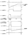
同図(a)には、電流制御発振回路7の出力信号「A」の波形を示す。また、同図(b)および(c)には、電流制御発振回路7の2つのインバータ回路14,15の出力信号「B」と「C」を示す。
2,3 ドライバ回路
4 負荷回路
6 誤差増幅回路
7 電流制御発振回路
8 パルス生成回路
9 デッドタイム生成回路
10 PFM制御回路
11 レベルシフト回路
12 リセット回路
13 コンパレータ回路
20 出力段
50 過電流検出回路
Mp,Mn スイッチ素子
Claims (5)
- 入力電源の高電位側に接続される第1スイッチ素子、
前記第1スイッチ素子と直列に接続され入力電源の低電位側に接続される第2スイッチ素子、
前記第1スイッチ素子と前記第2スイッチ素子の接続点に接続され負荷回路に平滑出力電圧を供給するインダクタと平滑容量からなるフィルタ回路、
前記負荷回路の出力電圧を検出して負帰還信号を出力する電圧検出回路、
前記負帰還信号と第1の基準電圧を比較増幅して前記第1スイッチ素子および前記第2スイッチ素子をスイッチングする制御信号を出力する制御回路、
および前記制御信号により前記第1スイッチ素子と前記第2スイッチ素子を交互に導通・遮断制御するドライバ回路、
を備えたDC−DCコンバータにおいて、
前記第2スイッチ素子の導通制御時に、前記第2スイッチ素子での電圧降下を第2の基準電圧と比較することによって前記インダクタに流れるインダクタ電流を検出し、前記インダクタ電流が所定の大きさまで低減したか否かを判定する過電流検出手段と、
前記過電流検出手段で前記インダクタ電流が前記所定の大きさに低減したと判定されるまで前記第1スイッチ素子の遮断制御時間を延長するように、前記制御信号のスイッチングタイミングを変更するタイミング変更手段と、
を有し、
前記過電流検出手段は、
前記第2スイッチ素子のドレイン・ソース間電圧に所定の電圧を加算して出力するレベルシフト回路と、
前記第2スイッチ素子の遮断制御時に前記レベルシフト回路からの出力信号を所定値に固定するリセット回路と、
前記第2スイッチ素子の導通制御時に前記レベルシフト回路からの出力信号電圧が前記第2の基準電圧に到達したかどうかを判定する判定回路と、
を備えたことを特徴とするDC−DCコンバータ。 - 前記制御回路は、
前記負帰還信号と前記第1の基準電圧の誤差を増幅する誤差増幅回路と、
前記誤差増幅回路の出力に応じた発振周波数のパルス信号を生成する発振回路と、
前記パルス信号に基づいて前記制御信号を生成するパルス生成回路を備え、
前記パルス生成回路では、前記第1スイッチ素子に対する導通制御時間を固定するとともに、その遮断制御時間を延長変更可能としたことを特徴とする請求項1記載のDC−DCコンバータ。 - 前記タイミング変更手段は、前記過電流検出手段において前記インダクタ電流が前記所定の大きさ以上であると判定されている間、前記発振回路の発振動作を停止制御するようにしたことを特徴とする請求項2記載のDC−DCコンバータ。
- 前記発振回路は、リングオシレータであることを特徴とする請求項2記載のDC−DCコンバータ。
- 前記制御回路と前記ドライバ回路の間には、前記第1スイッチ素子と前記第2スイッチ素子を同時に遮断制御するデッドタイムを設定するデッドタイム生成回路が接続されていることを特徴とする請求項1ないし4のいずれかに記載のDC−DCコンバータ。
Priority Applications (3)
| Application Number | Priority Date | Filing Date | Title |
|---|---|---|---|
| JP2007070530A JP4985003B2 (ja) | 2007-03-19 | 2007-03-19 | Dc−dcコンバータ |
| CN2008100055494A CN101272094B (zh) | 2007-03-19 | 2008-02-15 | Dc-dc转换器 |
| US12/051,556 US8013585B2 (en) | 2007-03-19 | 2008-03-19 | DC-DC converter and DC-DC power conversion method employing overcurrent protection |
Applications Claiming Priority (1)
| Application Number | Priority Date | Filing Date | Title |
|---|---|---|---|
| JP2007070530A JP4985003B2 (ja) | 2007-03-19 | 2007-03-19 | Dc−dcコンバータ |
Publications (2)
| Publication Number | Publication Date |
|---|---|
| JP2008236859A JP2008236859A (ja) | 2008-10-02 |
| JP4985003B2 true JP4985003B2 (ja) | 2012-07-25 |
Family
ID=39774025
Family Applications (1)
| Application Number | Title | Priority Date | Filing Date |
|---|---|---|---|
| JP2007070530A Expired - Fee Related JP4985003B2 (ja) | 2007-03-19 | 2007-03-19 | Dc−dcコンバータ |
Country Status (3)
| Country | Link |
|---|---|
| US (1) | US8013585B2 (ja) |
| JP (1) | JP4985003B2 (ja) |
| CN (1) | CN101272094B (ja) |
Cited By (1)
| Publication number | Priority date | Publication date | Assignee | Title |
|---|---|---|---|---|
| KR101812013B1 (ko) * | 2016-11-03 | 2018-01-25 | 주식회사 유비쿼스 | 순간적인 과전류로 인한 역방향 전력공급용 디바이스의 불필요한 동작중단을 방지하는 방법 및 그 장치 |
Families Citing this family (30)
| Publication number | Priority date | Publication date | Assignee | Title |
|---|---|---|---|---|
| US7995359B2 (en) | 2009-02-05 | 2011-08-09 | Power Integrations, Inc. | Method and apparatus for implementing an unregulated dormant mode with an event counter in a power converter |
| US7952895B2 (en) | 2008-05-29 | 2011-05-31 | Power Integrations, Inc. | Method and apparatus for implementing an unregulated dormant mode in a power converter |
| JP2011015557A (ja) * | 2009-07-02 | 2011-01-20 | Panasonic Corp | スイッチング電源装置およびスイッチング電源制御用半導体装置 |
| KR101677731B1 (ko) * | 2009-12-31 | 2016-11-18 | 페어차일드코리아반도체 주식회사 | 자동 재 시작 회로 및 그 방법 |
| US8797009B2 (en) * | 2010-07-06 | 2014-08-05 | Csr Technology Inc. | Auto cascode buck voltage converter |
| DE102010038623A1 (de) * | 2010-07-29 | 2012-02-02 | Robert Bosch Gmbh | Schaltungsanordnung und Verfahren zur Begrenzung von Stromstärke und/oder Flankensteilheit elektrischer Signale |
| JP2012039710A (ja) * | 2010-08-05 | 2012-02-23 | Sanken Electric Co Ltd | スイッチング電源装置 |
| JP2012039761A (ja) * | 2010-08-06 | 2012-02-23 | Sanken Electric Co Ltd | スイッチング電源装置 |
| JP2012044784A (ja) | 2010-08-19 | 2012-03-01 | Sanken Electric Co Ltd | スイッチング電源装置 |
| US8334683B2 (en) * | 2010-08-24 | 2012-12-18 | Intersil Americas Inc. | System and method for current limiting a DC-DC converter |
| US8698470B2 (en) | 2011-02-28 | 2014-04-15 | Texas Instruments Incorporated | Control for switching between PWM and PFM operation in a buck converter |
| TW201246769A (en) * | 2011-05-10 | 2012-11-16 | Hon Hai Prec Ind Co Ltd | Buck converter |
| CN102594139A (zh) * | 2012-03-06 | 2012-07-18 | 隆鑫通用动力股份有限公司 | 一种基于UCx84x的DC-DC电源转换器 |
| CN103378726B (zh) * | 2012-04-18 | 2015-08-19 | 立锜科技股份有限公司 | 切换式电源供应器及其控制电路与控制方法 |
| CN103424605A (zh) * | 2012-05-19 | 2013-12-04 | 快捷半导体(苏州)有限公司 | 一种零电流检测电路和方法、及电压变换电路 |
| US9036383B2 (en) * | 2012-09-19 | 2015-05-19 | Fuji Electric Co., Ltd. | Power supply device control circuit |
| KR101378512B1 (ko) | 2013-01-25 | 2014-03-27 | 주식회사 하이딥 | 동기형 dc-dc 컨버터 |
| US11159009B2 (en) * | 2013-04-01 | 2021-10-26 | Qualcomm Incorporated | Voltage regulator over-current protection |
| US9194896B2 (en) * | 2013-04-05 | 2015-11-24 | Texas Instruments Incorporated | Tracking energy consumption using a sepic-converter technique |
| JP6148551B2 (ja) * | 2013-06-26 | 2017-06-14 | 株式会社東芝 | 整流装置 |
| TWI496403B (zh) * | 2013-08-07 | 2015-08-11 | Richtek Technology Corp | 電壓轉換控制器及電壓轉換電路 |
| CN107112995B (zh) * | 2014-12-17 | 2020-11-03 | 三菱电机株式会社 | 电平移位电路、集成电路及功率半导体模块 |
| RU2604662C1 (ru) * | 2015-07-16 | 2016-12-10 | Акционерное общество "Научно-производственное объединение автоматики имени академика Н.А. Семихатова" | Резервированный источник питания постоянного напряжения |
| FR3060904B1 (fr) * | 2016-12-15 | 2023-10-27 | 3D Plus | Convertisseur de tension haute frequence continue de type buck quasi-resonant |
| US10063132B1 (en) * | 2017-02-28 | 2018-08-28 | Dialog Semiconductor (Uk) Limited | Over-current protection circuit |
| RU2663238C1 (ru) * | 2017-04-21 | 2018-08-03 | Акционерное общество "Авиаавтоматика" имени В.В. Тарасова" | Способ построения модульного источника питания повышенной надежности и модульный источник питания |
| KR102380354B1 (ko) * | 2017-09-29 | 2022-03-31 | 현대자동차주식회사 | 전자 회로 모듈 및 이를 포함하는 차량 |
| JP6500146B2 (ja) * | 2018-04-19 | 2019-04-10 | ローム株式会社 | 過電流保護回路 |
| GB2606373A (en) * | 2021-05-05 | 2022-11-09 | Eaton Intelligent Power Ltd | Power inverter and method for controlling a power inverter |
| CN116931642B (zh) * | 2023-09-13 | 2023-12-19 | 浙江地芯引力科技有限公司 | 带隙基准电压源及带隙基准电路 |
Family Cites Families (9)
| Publication number | Priority date | Publication date | Assignee | Title |
|---|---|---|---|---|
| JP3469131B2 (ja) * | 1999-07-09 | 2003-11-25 | シャープ株式会社 | 直流安定化電源装置 |
| US6577110B2 (en) * | 2001-01-12 | 2003-06-10 | Sipex Corporation | DC-to-DC converter with constant ripple current regulation for continuous and discontinuous conduction mode operation |
| JP2002325438A (ja) * | 2001-04-24 | 2002-11-08 | Fujitsu Ltd | 同期整流コンバータ |
| JP3801021B2 (ja) * | 2001-06-15 | 2006-07-26 | 株式会社村田製作所 | 自励式チョッパレギュレータ、それに用いる電圧制御モジュールおよびそれを用いた電子機器 |
| JP2004364488A (ja) * | 2003-05-12 | 2004-12-24 | Taiyo Yuden Co Ltd | スイッチング電源回路およびその過電流保護方法 |
| JP3748262B2 (ja) * | 2003-06-24 | 2006-02-22 | ローム株式会社 | スイッチング型直流−直流コンバータ |
| JP2005304210A (ja) * | 2004-04-14 | 2005-10-27 | Renesas Technology Corp | 電源ドライバ装置及びスイッチング電源装置 |
| US7045993B1 (en) * | 2004-04-29 | 2006-05-16 | National Semiconductor Corporation | Apparatus and method for step-down switching voltage regulation |
| TW200713768A (en) * | 2005-09-05 | 2007-04-01 | Niko Semiconductor Co Ltd | Auto-adaptive voltage positioning high-speed PWM controlling device and driving signal generation method thereof |
-
2007
- 2007-03-19 JP JP2007070530A patent/JP4985003B2/ja not_active Expired - Fee Related
-
2008
- 2008-02-15 CN CN2008100055494A patent/CN101272094B/zh not_active Expired - Fee Related
- 2008-03-19 US US12/051,556 patent/US8013585B2/en not_active Expired - Fee Related
Cited By (1)
| Publication number | Priority date | Publication date | Assignee | Title |
|---|---|---|---|---|
| KR101812013B1 (ko) * | 2016-11-03 | 2018-01-25 | 주식회사 유비쿼스 | 순간적인 과전류로 인한 역방향 전력공급용 디바이스의 불필요한 동작중단을 방지하는 방법 및 그 장치 |
Also Published As
| Publication number | Publication date |
|---|---|
| CN101272094B (zh) | 2012-11-28 |
| US8013585B2 (en) | 2011-09-06 |
| US20080231244A1 (en) | 2008-09-25 |
| CN101272094A (zh) | 2008-09-24 |
| JP2008236859A (ja) | 2008-10-02 |
Similar Documents
| Publication | Publication Date | Title |
|---|---|---|
| JP4985003B2 (ja) | Dc−dcコンバータ | |
| TWI709288B (zh) | 用於電壓調節器之過電流保護電路及方法 | |
| KR101302899B1 (ko) | 로우 스탠드바이 전류 스위칭 레귤레이터를 위한 방법 및 장치 | |
| JP5493296B2 (ja) | スイッチングレギュレータ | |
| JP5586211B2 (ja) | Dc−dcコンバータおよび半導体集積回路 | |
| JP6278188B2 (ja) | Dc/dcコンバータ | |
| US8471540B2 (en) | DC-DC converter | |
| TWI483528B (zh) | 直流對直流轉換器電路及偵測直流對直流轉換器電路內之零電流交跨的偵測電路和方法以及其電源供應器控制器、電源供應器、系統 | |
| JP6209022B2 (ja) | スイッチングレギュレータ | |
| KR20090028498A (ko) | 스위칭 레귤레이터 및 그 제어 방법 | |
| JP5034399B2 (ja) | スイッチングレギュレータ | |
| US9979288B2 (en) | Switching mode power supply with adaptive frequency | |
| JP2010136510A (ja) | 降圧型スイッチングレギュレータ | |
| JP2009148094A (ja) | Dc−dcコンバータおよび電源制御用半導体集積回路 | |
| JP2007053892A (ja) | Dc−dcコンバータ | |
| JP4548100B2 (ja) | Dc−dcコンバータ | |
| JP5839863B2 (ja) | 降圧スイッチングレギュレータおよびその制御回路ならびにそれを用いた電子機器 | |
| JP2011091888A (ja) | スイッチング制御回路及びこれを用いたスイッチング電源装置 | |
| CN107086778B (zh) | 降压调节器的低功率待机模式 | |
| JP4837352B2 (ja) | スイッチングレギュレータおよびその駆動方法 | |
| JP5287261B2 (ja) | Dc−dcコンバータ | |
| JP2007135287A (ja) | Dc−dcコンバータ | |
| US11081957B2 (en) | Power converter with multi-mode timing control | |
| TWI817533B (zh) | 切換模式電力供應器(smps)及相關控制器與方法 | |
| JP6341423B2 (ja) | Dc/dcコンバータ |
Legal Events
| Date | Code | Title | Description |
|---|---|---|---|
| A621 | Written request for application examination |
Free format text: JAPANESE INTERMEDIATE CODE: A621 Effective date: 20090714 |
|
| A711 | Notification of change in applicant |
Free format text: JAPANESE INTERMEDIATE CODE: A712 Effective date: 20091112 |
|
| RD03 | Notification of appointment of power of attorney |
Free format text: JAPANESE INTERMEDIATE CODE: A7423 Effective date: 20091112 |
|
| RD04 | Notification of resignation of power of attorney |
Free format text: JAPANESE INTERMEDIATE CODE: A7424 Effective date: 20091112 |
|
| A711 | Notification of change in applicant |
Free format text: JAPANESE INTERMEDIATE CODE: A712 Effective date: 20110422 |
|
| A131 | Notification of reasons for refusal |
Free format text: JAPANESE INTERMEDIATE CODE: A131 Effective date: 20111115 |
|
| A977 | Report on retrieval |
Free format text: JAPANESE INTERMEDIATE CODE: A971007 Effective date: 20111116 |
|
| A521 | Request for written amendment filed |
Free format text: JAPANESE INTERMEDIATE CODE: A523 Effective date: 20111229 |
|
| TRDD | Decision of grant or rejection written | ||
| A01 | Written decision to grant a patent or to grant a registration (utility model) |
Free format text: JAPANESE INTERMEDIATE CODE: A01 Effective date: 20120403 |
|
| A01 | Written decision to grant a patent or to grant a registration (utility model) |
Free format text: JAPANESE INTERMEDIATE CODE: A01 |
|
| A61 | First payment of annual fees (during grant procedure) |
Free format text: JAPANESE INTERMEDIATE CODE: A61 Effective date: 20120416 |
|
| R150 | Certificate of patent or registration of utility model |
Ref document number: 4985003 Country of ref document: JP Free format text: JAPANESE INTERMEDIATE CODE: R150 Free format text: JAPANESE INTERMEDIATE CODE: R150 |
|
| FPAY | Renewal fee payment (event date is renewal date of database) |
Free format text: PAYMENT UNTIL: 20150511 Year of fee payment: 3 |
|
| R250 | Receipt of annual fees |
Free format text: JAPANESE INTERMEDIATE CODE: R250 |
|
| R250 | Receipt of annual fees |
Free format text: JAPANESE INTERMEDIATE CODE: R250 |
|
| R250 | Receipt of annual fees |
Free format text: JAPANESE INTERMEDIATE CODE: R250 |
|
| R250 | Receipt of annual fees |
Free format text: JAPANESE INTERMEDIATE CODE: R250 |
|
| R250 | Receipt of annual fees |
Free format text: JAPANESE INTERMEDIATE CODE: R250 |
|
| R250 | Receipt of annual fees |
Free format text: JAPANESE INTERMEDIATE CODE: R250 |
|
| R250 | Receipt of annual fees |
Free format text: JAPANESE INTERMEDIATE CODE: R250 |
|
| R250 | Receipt of annual fees |
Free format text: JAPANESE INTERMEDIATE CODE: R250 |
|
| LAPS | Cancellation because of no payment of annual fees |