JP4985003B2 - DC-DC converter - Google Patents
DC-DC converter Download PDFInfo
- Publication number
- JP4985003B2 JP4985003B2 JP2007070530A JP2007070530A JP4985003B2 JP 4985003 B2 JP4985003 B2 JP 4985003B2 JP 2007070530 A JP2007070530 A JP 2007070530A JP 2007070530 A JP2007070530 A JP 2007070530A JP 4985003 B2 JP4985003 B2 JP 4985003B2
- Authority
- JP
- Japan
- Prior art keywords
- circuit
- switch element
- control
- voltage
- signal
- Prior art date
- Legal status (The legal status is an assumption and is not a legal conclusion. Google has not performed a legal analysis and makes no representation as to the accuracy of the status listed.)
- Expired - Fee Related
Links
- 238000001514 detection method Methods 0.000 claims description 41
- 230000010355 oscillation Effects 0.000 claims description 24
- 239000003990 capacitor Substances 0.000 claims description 11
- 230000003321 amplification Effects 0.000 claims description 7
- 238000003199 nucleic acid amplification method Methods 0.000 claims description 7
- 238000009499 grossing Methods 0.000 claims description 3
- 230000007423 decrease Effects 0.000 description 8
- 238000010586 diagram Methods 0.000 description 6
- 238000000034 method Methods 0.000 description 4
- 230000001360 synchronised effect Effects 0.000 description 2
- 238000007796 conventional method Methods 0.000 description 1
- 230000005669 field effect Effects 0.000 description 1
- 239000004065 semiconductor Substances 0.000 description 1
- 239000000758 substrate Substances 0.000 description 1
Images


Classifications
-
- H—ELECTRICITY
- H02—GENERATION; CONVERSION OR DISTRIBUTION OF ELECTRIC POWER
- H02M—APPARATUS FOR CONVERSION BETWEEN AC AND AC, BETWEEN AC AND DC, OR BETWEEN DC AND DC, AND FOR USE WITH MAINS OR SIMILAR POWER SUPPLY SYSTEMS; CONVERSION OF DC OR AC INPUT POWER INTO SURGE OUTPUT POWER; CONTROL OR REGULATION THEREOF
- H02M3/00—Conversion of dc power input into dc power output
- H02M3/02—Conversion of dc power input into dc power output without intermediate conversion into ac
- H02M3/04—Conversion of dc power input into dc power output without intermediate conversion into ac by static converters
- H02M3/10—Conversion of dc power input into dc power output without intermediate conversion into ac by static converters using discharge tubes with control electrode or semiconductor devices with control electrode
- H02M3/145—Conversion of dc power input into dc power output without intermediate conversion into ac by static converters using discharge tubes with control electrode or semiconductor devices with control electrode using devices of a triode or transistor type requiring continuous application of a control signal
- H02M3/155—Conversion of dc power input into dc power output without intermediate conversion into ac by static converters using discharge tubes with control electrode or semiconductor devices with control electrode using devices of a triode or transistor type requiring continuous application of a control signal using semiconductor devices only
- H02M3/156—Conversion of dc power input into dc power output without intermediate conversion into ac by static converters using discharge tubes with control electrode or semiconductor devices with control electrode using devices of a triode or transistor type requiring continuous application of a control signal using semiconductor devices only with automatic control of output voltage or current, e.g. switching regulators
- H02M3/158—Conversion of dc power input into dc power output without intermediate conversion into ac by static converters using discharge tubes with control electrode or semiconductor devices with control electrode using devices of a triode or transistor type requiring continuous application of a control signal using semiconductor devices only with automatic control of output voltage or current, e.g. switching regulators including plural semiconductor devices as final control devices for a single load
-
- H—ELECTRICITY
- H02—GENERATION; CONVERSION OR DISTRIBUTION OF ELECTRIC POWER
- H02M—APPARATUS FOR CONVERSION BETWEEN AC AND AC, BETWEEN AC AND DC, OR BETWEEN DC AND DC, AND FOR USE WITH MAINS OR SIMILAR POWER SUPPLY SYSTEMS; CONVERSION OF DC OR AC INPUT POWER INTO SURGE OUTPUT POWER; CONTROL OR REGULATION THEREOF
- H02M1/00—Details of apparatus for conversion
- H02M1/32—Means for protecting converters other than automatic disconnection
Description
本発明は、負荷回路に所定の大きさで直流電圧を供給するDC−DCコンバータに関し、とくに過電流保護機能を有するDC−DCコンバータに関する。 The present invention relates to a DC-DC converter that supplies a DC voltage with a predetermined magnitude to a load circuit, and more particularly to a DC-DC converter having an overcurrent protection function.
従来、ノート型のパーソナルコンピュータや携帯電話、その他の携帯用電子機器等では、バッテリ電圧を降圧型スイッチング電源回路からなるDC−DCコンバータによって規定電圧まで降圧して電子回路に供給して駆動している。その場合に、スイッチ素子を過電流から保護する過電流保護回路が使用される。 Conventionally, in notebook personal computers, mobile phones, and other portable electronic devices, the battery voltage is stepped down to a specified voltage by a DC-DC converter composed of a step-down switching power supply circuit and supplied to an electronic circuit for driving. Yes. In this case, an overcurrent protection circuit that protects the switch element from overcurrent is used.
図5は、インダクタ電流ILのピーク制限によって過電流保護を行う、従来のDC−DCコンバータの一例を示す図である。
この種のDC−DCコンバータは、バッテリからの入力電圧Vinにソース端子が接続されたPチャネル型の電界効果トランジスタ(FET)からなる第1のスイッチング半導体素子(以下、スイッチ素子という)Mpと、ソース端子が接地されたNチャネル型のFETからなる第2のスイッチ素子Mnとを、互いのドレイン端子を接続するとともに、それぞれのゲート端子にスイッチング制御回路1からドライバ回路2,3を介して制御信号を供給するように構成されている。スイッチ素子Mpとスイッチ素子Mnの接続点には、インダクタLを介して充電・平滑用の出力コンデンサCoutと負荷回路4とが、それぞれ他端が接地されて接続されている。
Figure 5 performs overcurrent protection by the peak limits the inductor current I L, which is a diagram illustrating an example of a conventional DC-DC converter.
This type of DC-DC converter includes a first switching semiconductor element (hereinafter referred to as a switching element) Mp composed of a P-channel field effect transistor (FET) having a source terminal connected to an input voltage Vin from a battery, The second switch element Mn made of an N-channel FET whose source terminal is grounded is connected to the respective drain terminals and controlled to each gate terminal from the
インダクタLと出力コンデンサCoutは、負荷回路4に平滑出力電圧を供給するフィルタ回路を構成している。この負荷回路4に対する出力電圧Voutを検出するために、スイッチング制御回路1に出力電圧Voutが負帰還信号として供給されている。スイッチング制御回路1で出力電圧Voutを監視しつつ、この出力電圧Voutが一定値となるように、図示しないドライバ回路を介してスイッチ素子Mpとスイッチ素子Mnに制御信号を出力し、これらが交互に導通・遮断するように制御している。
The inductor L and the output capacitor Cout constitute a filter circuit that supplies a smooth output voltage to the load circuit 4. In order to detect the output voltage Vout for the load circuit 4, the output voltage Vout is supplied to the
過電流検出回路5は、たとえばカレントトランス、もしくはセンス抵抗と増幅器などによりスイッチ素子Mpに流れる電流、すなわちスイッチ素子MpからインダクタLに流れ込むインダクタ電流ILを検出し、これを所定の基準値と比較することにより過電流を検知している。この過電流検出回路5で過電流が検知された場合、スイッチング制御回路1がスイッチ素子Mpを遮断状態に制御するように構成されている。
従来のDC−DCコンバータでは、通常のスイッチング動作を実行している間は、スイッチング制御回路1がその出力電圧Voutの変化に応じてスイッチ素子Mpとスイッチ素子Mnを導通・遮断制御するパルス信号のパルス幅を変化させて、出力電圧Voutが一定となるように帰還制御を行う。これにより、負荷回路4への供給電流Ioutが大きい重負荷のときにも、スイッチ素子Mpが遮断状態の間に負荷に応じてインダクタLに蓄えられたエネルギーがスイッチ素子Mnを介して放出されるので、効率の良い同期整流を行うことができる。
In the conventional DC-DC converter, while the normal switching operation is being performed, the
DC−DCコンバータの入力電圧Vin側のスイッチ素子Mpに流れる電流(=IL)が規定値Ipmaxを超えると、過電流検出回路5で過電流検出信号が出力され、スイッチング制御回路1を介してつぎのスイッチング周期までスイッチ素子Mpを遮断制御状態とする。こうして、過電流検出回路5によるインダクタ電流ILのピーク電流値Ipを規定値Ipmax以下に制限する過電流制限機能が実現される。
When the current (= I L ) flowing through the switch element Mp on the input voltage Vin side of the DC-DC converter exceeds the specified value Ipmax, an overcurrent detection signal is output from the
しかし、実際の過電流検出回路5で規定値Ipmaxを超える電流が検知された後、スイッチ素子Mpをスイッチングしてオフするまでには、一定の遅延時間が必要である。そのため、スイッチング制御回路1からのドライブ信号でスイッチ素子Mpが導通制御状態に移行した瞬間に過電流状態を検知したとしても、過電流検出回路5を介して実際にスイッチ素子Mpが遮断状態になるまでの間は、インダクタ電流ILが継続して増加することになる。
However, after a current exceeding the specified value Ipmax is detected by the actual
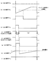
図6は、出力電圧Voutが大きい場合と小さい場合とで、従来のDC−DCコンバータの過電流保護機能が作動している状態で、インダクタ電流がそれぞれどのように変化するかを示している。同図(a)は出力電圧Voutが大きな場合、同図(b)は出力電圧Voutが小さな場合であって、それぞれ縦軸にはインダクタ電流ILを、横軸には時間を示している。 FIG. 6 shows how the inductor current changes depending on whether the output voltage Vout is large or small and the overcurrent protection function of the conventional DC-DC converter is operating. 4A shows a case where the output voltage Vout is large, and FIG. 4B shows a case where the output voltage Vout is small. The vertical axis shows the inductor current IL and the horizontal axis shows time.
ここでは、インダクタ電流ILが規定値Ipmaxを超えた場合に、スイッチ素子Mpを遮断制御状態とするのに要する最低限の遅延時間をTdとする。インダクタ電流ILの減少率は出力電圧Voutに比例するため(dIL/dt=Vout/L)、図6(b)に示すように、出力電圧Voutが低い場合は、高い場合と比較して、インダクタ電流ILの減少に長い時間が必要となる。逆に、インダクタ電流ILの増加率は、出力電圧Voutが低いほど大きい(dIL/dt=(Vin−Vout)/L)。このため、図(b)に示すように、インダクタ電流ILが規定値Ipmaxを超えた後も、遅延時間Tdでインダクタ電流ILが大きな傾斜で上昇しつづける。すると、スイッチ素子Mpが遮断制御されている時間内では、それまでに増加したインダクタ電流ILが減少しきれないままつぎのスイッチング周期でインダクタ電流ILが上昇を始める。 Here, when the inductor current I L has exceeded the prescribed value Ipmax, and Td the minimum delay time required for the switch element Mp and cutoff control state. Since the decrease rate of the inductor current I L is proportional to the output voltage Vout (dI L / dt = Vout / L), as shown in FIG. 6B, when the output voltage Vout is low, it is higher than when it is high. , a long time the decrease in inductor current I L is required. Conversely, the increase rate of the inductor current I L increases as the output voltage Vout decreases (dI L / dt = (Vin−Vout) / L). Therefore, as shown in FIG. (B), after the inductor current I L has exceeded the prescribed value Ipmax also continue to increase the inductor current I L by the delay time Td is a large gradient. Then, within the time during which the switching element Mp is controlled to be cut off, the inductor current I L starts to rise in the next switching period without the inductor current I L that has increased so far being reduced.
このように、従来の過電流検出回路5による過電流検出では、インダクタ電流ILの過電流制限機能が有効に働かなくなるおそれがあった。しかも、過電流を検出してからの遅延時間Tdが一定であれば、スイッチング制御回路1でのスイッチング周波数が上昇するほど、正常に過電流制限を機能させることは困難となる。
Thus, in the overcurrent detection by the conventional
そこで、こうしたスイッチング電源において、最小オンデューティ時間(Tmin)でインダクタ電流(IL)が増加してしまうのを防止するスイッチング電源回路の過電流保護方法が考えられている(たとえば、特許文献1参照)。 Thus, in such a switching power supply, an overcurrent protection method for a switching power supply circuit that prevents an increase in inductor current (I L ) with a minimum on-duty time (Tmin) has been considered (for example, see Patent Document 1). ).
この特許文献1には、スイッチング素子であるトランジスタ(2)からインダクタに流れる電流(I−H)を検出する過電流検出回路(221)と、スイッチング素子がオフしたときのフライホイール電流(I−L)を検出する電流検出回路(230)とを設け、過電流検出回路(221)で電流(I−H)(=インダクタ電流)値がある所定値を超えていることを検出すると、電流検出回路(230)でフライホイール電流が別の所定値以下になるのを検出するまでスイッチング素子のスイッチング動作をマスクして止める技術が開示されている。
上述した特許文献1の過電流保護方法は、トランジスタ(2)からインダクタに流れる電流(I−H)とフライホイール電流(I−L)をそれぞれ検出するために、2つの検出回路が必要とされているため、スイッチング電源回路のコストアップにつながるという問題があった。
The overcurrent protection method of
また、特許文献1に記載された過電流保護動作では、スイッチング素子の駆動パルスからマスクを外すタイミングと、その後に最初にスイッチング素子に対するPWMパルスの供給タイミングとで、互いに同期をとることを想定していない。このため、インダクタ電流のボトム値が両者のタイミングによってばらつき、インダクタ電流の平均値を予測することができなくなって、的確なスイッチング制御が難しくなるという問題があった。この問題点は、とくにスイッチング素子のスイッチング周波数が低い場合に顕著に表われる。
Further, in the overcurrent protection operation described in
さらに、固定オン時間方式のPFM制御に適用される過電流保護回路では、過電流制限により出力電圧が低下した場合に、定電圧制御を行う制御回路が出力電圧を上昇させようとしてスイッチング周波数が上昇し続けるため、従来方式による過電流制限機能は有効に動作しないという問題もあった。 Furthermore, in the overcurrent protection circuit applied to the PFM control of the fixed on-time method, when the output voltage decreases due to overcurrent limitation, the control circuit that performs constant voltage control increases the switching voltage to increase the output voltage. Therefore, there is a problem that the overcurrent limiting function according to the conventional method does not operate effectively.
このような場合に何らかの手段でスイッチング周波数に上限を設けて対処することも可能であるが、DC−DCコンバータの過電流保護回路は、ある程度まで周波数に余裕を見込んで設計する必要がある。すなわち、通常動作で使用する周波数より高い周波数であっても、過電流状態に確実に対応可能な過電流制限機能を必要としていた。 In such a case, it is possible to provide an upper limit for the switching frequency by some means, but the overcurrent protection circuit of the DC-DC converter needs to be designed with a certain margin in frequency. That is, an overcurrent limiting function that can reliably cope with an overcurrent state is required even at a higher frequency than that used in normal operation.
本発明はこのような点に鑑みてなされたものであり、過電流検出動作に遅延があっても、過電流制限不能に陥るおそれのないDC−DCコンバータを提供することを目的とする。 The present invention has been made in view of these points, and an object of the present invention is to provide a DC-DC converter that does not fall into an overcurrent limit impossible even if there is a delay in the overcurrent detection operation.
本発明では、上記問題を解決するために、入力電源の高電位側に接続される第1スイッチ素子、前記第1スイッチ素子と直列に接続され入力電源の低電位側に接続される第2スイッチ素子、前記第1スイッチ素子と前記第2スイッチ素子の接続点に接続され負荷回路に平滑出力電圧を供給するインダクタと平滑容量からなるフィルタ回路、前記負荷回路の出力電圧を検出して負帰還信号を出力する電圧検出回路、前記負帰還信号と第1の基準電圧を比較増幅して前記第1スイッチ素子および前記第2スイッチ素子をスイッチングする制御信号を出力する制御回路、および前記制御信号により前記第1スイッチ素子と前記第2スイッチ素子を交互に導通・遮断制御するドライバ回路、を備えたDC−DCコンバータにおいて、前記第2スイッチ素子の導通制御時に、前記第2スイッチ素子での電圧降下を第2の基準電圧と比較することによって前記インダクタに流れるインダクタ電流を検出し、前記インダクタ電流が所定の大きさまで低減したか否かを判定する過電流検出手段と、前記過電流検出手段で前記インダクタ電流が前記所定の大きさに低減したと判定されるまで前記第1スイッチ素子の遮断制御時間を延長するように、前記制御信号のスイッチングタイミングを変更するタイミング変更手段と、を有し、前記過電流検出手段は、前記第2スイッチ素子のドレイン・ソース間電圧に所定の電圧を加算して出力するレベルシフト回路と、前記第2スイッチ素子の遮断制御時に前記レベルシフト回路からの出力信号を所定値に固定するリセット回路と、前記第2スイッチ素子の導通制御時に前記レベルシフト回路からの出力信号電圧が前記第2の基準電圧に到達したかどうかを判定する判定回路と、を備えたことを特徴とするDC−DCコンバータが提供される。
In the present invention, in order to solve the above problem, the first switch element connected to the high potential side of the input power supply, and the second switch connected in series with the first switch element and connected to the low potential side of the input power supply Element, a filter circuit comprising a smoothing capacitor connected to a connection point of the first switch element and the second switch element and supplying a smooth output voltage to the load circuit, and a negative feedback signal by detecting the output voltage of the load circuit A voltage detection circuit that outputs a control signal for comparing and amplifying the negative feedback signal and a first reference voltage to switch the first switch element and the second switch element, and the control signal A DC-DC converter comprising a driver circuit that alternately conducts and shuts off the first switch element and the second switch element, wherein the second switch During the conduction control of the child, said second voltage drop across the switching device detects the inductor current flowing through the inductor by comparing a second reference voltage, whether the inductor current is reduced to a predetermined size An overcurrent detection means for determining, and the control signal of the control signal so as to extend the cutoff control time of the first switch element until it is determined by the overcurrent detection means that the inductor current has been reduced to the predetermined magnitude. possess timing changing means for changing the switching timing, and the overcurrent detecting means, a level shift circuit for outputting by adding a predetermined voltage to the drain-source voltage of the second switching element, the second A reset circuit for fixing an output signal from the level shift circuit to a predetermined value during switching control of the switch element; DC-DC converter, wherein the output signal voltage from the level shift circuit when the control is provided with a determination circuit for determining whether or has reached the second reference voltage is provided.
本発明のDC−DCコンバータによれば、出力電圧が低下したときに、過電流制限不能に陥るおそれがなく、固定オン時間PFMコンバータにも適したものが構成できる。 According to the DC-DC converter of the present invention, when the output voltage is lowered, there is no possibility that the overcurrent limitation cannot be performed, and it is possible to configure the converter suitable for the fixed on-time PFM converter.
以下、図面を参照してこの発明の実施の形態について説明する。
図1は、この発明のDC−DCコンバータの原理的な構成を示すブロック図である。図1では、図5に示す従来のものと同じ部分には同一参照番号を付けている。
Embodiments of the present invention will be described below with reference to the drawings.
FIG. 1 is a block diagram showing the basic configuration of the DC-DC converter of the present invention. In FIG. 1, the same reference numerals are assigned to the same parts as those of the conventional one shown in FIG.
このDC−DCコンバータでは、インダクタ電流ILのボトム電流値(Ib)を制限するために、過電流検出回路50がスイッチ素子Mnのドレイン端子とインダクタLとの間に配置されている。
In this DC-DC converter, in order to limit bottom current value of the inductor current I L to (Ib), the
ここで、過電流検出回路50はスイッチング制御回路1に接続され、たとえばカレントトランス、もしくはセンス抵抗と増幅器などによりスイッチ素子Mnに流れる電流、すなわちスイッチ素子MnからインダクタLに流れるインダクタ電流ILを検出し、これを規定値Ibmaxと比較することによりインダクタ電流ILが規定値Ibmaxまで減少したか否かを判定する。スイッチング制御回路1では、過電流検出回路50でインダクタ電流ILが所定の大きさに低減したと判定されるまでスイッチ素子Mpの遮断制御時間を延長するように、制御信号のスイッチングタイミングを変更する。
Here, the
図2は、この発明のDC−DCコンバータにおいて、過電流保護機能が作動している状態でのインダクタ電流の大きさの変化を示す図であって、同図(a)は出力電圧Voutが大きな場合、同図(b)は出力電圧Voutが小さな場合である。なお、それぞれ縦軸にはインダクタ電流ILを、横軸には時間を示している。 FIG. 2 is a diagram showing a change in the magnitude of the inductor current when the overcurrent protection function is operating in the DC-DC converter of the present invention. FIG. 2A shows a large output voltage Vout. In this case, FIG. 5B shows the case where the output voltage Vout is small. The vertical axis represents the inductor current I L and the horizontal axis represents time.
図2(a)および(b)ともに、スイッチ素子Mnに流れるインダクタ電流ILが規定値Ibmaxを超えている間はスイッチング制御回路1によりスイッチ素子Mnのオン時間をT1あるいはT2だけ延長し、インダクタ電流ILが規定値Ibmax以下まで減少してからつぎのスイッチング周期に移行して、当該次のスイッチング周期においてインダクタ電流ILが規定値Ibmax以下の値から上昇するようにしている。すなわち、インダクタ電流ILのボトム電流値Ibを規定値Ibmax以下に制限するよう延長時間T1,T2を設けることによって、スイッチング制御回路1における過電流制限機能を確実なものとしている。
Figure 2 (a) and (b) together, while the inductor current I L flowing through the switching element Mn is greater than the prescribed value Ibmax is the on-time of the switching element Mn was extended by T1 or T2 by the switching
さらに、このスイッチング制御回路1では、インダクタ電流ILのピーク電流Ipの規定値Ipmaxもまた、スイッチ素子Mpのオン時間Tonに増加可能な範囲に制限できる。
Furthermore, in the switching
なぜならば、ピーク電流Ipは
Ip=Ib+Ton(Vin−Vout)/L
<Ibmax+Ton(Vin−Vout)/L
のように制限されることから、ピーク電流Ipの規定値Ipmaxを規定値Ibmaxにより定まるIbmax+Ton(Vin−Vout)/Lとすればよいからである。
Because, the peak current Ip is Ip = Ib + Ton (Vin−Vout) / L
<Ibmax + Ton (Vin−Vout) / L
This is because the specified value Ipmax of the peak current Ip may be set to Ibmax + Ton (Vin−Vout) / L determined by the specified value Ibmax.
また、オン時間TonにインダクタLに流れるインダクタ電流ILの平均値は、Ibmax+0.5Ton(Vin−Vout)/Lに等しいか、あるいは略等しい値になる。
ここで、VinはDC−DCコンバータへのバッテリからの入力電圧値、Voutは負荷回路4への出力電圧値、LはインダクタLのインダクタンス値である。したがって、このスイッチング制御回路1は、PFM(パルス周波数変調)方式のDC−DCコンバータのように、スイッチ素子Mpのオン時間Tonが常に一定で変化しない固定オン時間のスイッチング制御方式に適用して好適である。
The average value of the inductor current I L flowing through the ON time Ton in the inductor L, Ibmax + 0.5Ton (Vin-Vout ) / equal to L, or become substantially equal.
Here, Vin is an input voltage value from the battery to the DC-DC converter, Vout is an output voltage value to the load circuit 4, and L is an inductance value of the inductor L. Therefore, this switching
また、過電流検出回路50は、インダクタ電流ILが規定値Ibmaxを下回るまでスイッチング周期自体を延長するものであるから、従来の過電流検出回路5のように過電流検出動作に遅延時間があっても、過電流制限が不能となる危険性がなくなる。したがって、DC−DCコンバータの負荷回路4が短絡状態となった際にも、過電流制限が可能という利点を有している。
Further, the
つぎに、こうしたDC−DCコンバータの一例として、過電流保護回路を組み込んだPFMコンバータの具体的な構成と動作について説明する。
図3は、実施の形態に係るDC−DCコンバータを示す回路図である。
Next, a specific configuration and operation of a PFM converter incorporating an overcurrent protection circuit will be described as an example of such a DC-DC converter.
FIG. 3 is a circuit diagram illustrating the DC-DC converter according to the embodiment.
スイッチ素子Mpとスイッチ素子Mnとが直列に接続されて、出力段20を構成している。スイッチ素子Mpのソース端子は入力電源Vinの高電位側に接続され、そのドレイン端子はスイッチ素子Mnのドレイン端子に接続され、スイッチ素子Mnのソース端子は接地されている。
The switch element Mp and the switch element Mn are connected in series to constitute the
インダクタLと出力コンデンサCoutはフィルタ回路を構成しており、このフィルタ回路は出力段20のスイッチ素子Mpとスイッチ素子Mnの接続点に接続され、負荷回路4に平滑出力電圧を供給している。負荷回路4に対する出力電圧Voutは、抵抗R1,R2を直列接続した電圧検出回路を介して、PFM制御回路10に負帰還信号として供給されている。
The inductor L and the output capacitor Cout constitute a filter circuit, which is connected to the connection point between the switch element Mp and the switch element Mn of the
PFM制御回路10は、誤差増幅回路6、発振回路(電流制御発振回路)7、およびパルス生成回路8から構成されている。誤差増幅回路6は、負帰還信号と第1の基準電圧Vref1を比較増幅して、スイッチ素子Mpおよびスイッチ素子Mnのスイッチング制御に必要なエラー信号を出力するものであって、抵抗分圧された負帰還信号が一方の入力端子に、第1の基準電圧Vref1が他端の入力端子に供給されている。電流制御発振回路7は、誤差増幅回路6から出力されるエラー信号に応じた発振周波数のパルス信号を発振する。パルス生成回路8は、このパルス信号に基づいてデッドタイム生成回路9に対する制御信号を生成する。なお、図3に示す誤差増幅回路6はトランスコンダクタンスアンプで構成されているので、エラー信号は電流信号となる。
The
このPFM制御回路10は、デッドタイム生成回路9を介してドライバ回路2,3と接続されている。ここでは、パルス生成回路8からの制御信号によってスイッチ素子Mp,Mnを交互に導通・遮断制御するとき、デッドタイム(DT)生成回路9からドライバ回路2,3への制御信号に対して、スイッチ素子Mpとスイッチ素子Mnを同時に遮断制御するデッドタイムが設定される。
The
過電流検出回路50は、レベルシフト回路11、リセット回路12、コンパレータ回路13から構成され、スイッチ素子Mnの導通制御時にインダクタLに流れるインダクタ電流ILを検出し、インダクタ電流ILが所定の大きさまで低減したか否かを判定している。
つぎに、PFM制御回路10および過電流検出回路50の具体的構成について、さらに説明する。
電流制御発振回路7は、2つのPチャネル型のFET(以下、トランジスタという。)M1,M2からなるカレントミラー回路、インバータ回路14,15、コンデンサC1、およびノア(NOR)回路16から構成されている。トランジスタM1,M2の各ソース端子はバッテリの入力電圧Vinに接続され、トランジスタM1のドレイン端子、ゲート端子、およびトランジスタM2のゲート端子がそれぞれ誤差増幅回路6の出力端子と接続されている。また、トランジスタM2のドレイン端子はインバータ回路14の電源端子と接続されている。
Next, specific configurations of the
The current-controlled oscillation circuit 7 includes a current mirror circuit composed of two P-channel FETs (hereinafter referred to as transistors) M1 and M2,
インバータ回路14は、その出力端子にコンデンサC1が接続され、さらにインバータ回路15を介してノア回路16の一方の入力端子と接続され、ノア回路16の出力端子が電流制御発振回路7の出力端子を構成するとともに、そこからインバータ回路14の入力端子に至る帰還するループによってリングオシレータが形成されている。
The
このノア回路16には、その他方の入力端子に過電流検出回路50の出力信号「K」が入力され、リングオシレータのループ内で過電流検出回路50の出力に応じて発振を停止させる論理ゲートとして構成されている。
The NOR
パルス生成回路8は、インバータ回路17,18、抵抗R3およびコンデンサC2から構成されている。ここで、インバータ回路17の電源端子には、抵抗R3を介してバッテリからの入力電圧Vinが供給され、インバータ回路17の出力端子はコンデンサC2およびインバータ回路18と接続されている。このインバータ回路18の出力端子は、パルス生成回路8の出力端子としてデッドタイム生成回路9に接続されている。
The
過電流検出回路50のレベルシフト回路11は、Nチャネル型のFETからなるスイッチ素子Ms1と定電流源19とから構成されている。スイッチ素子Ms1は、その基板端子が接地され、ソース端子(図3においてスイッチ素子Ms1の右側の端子)およびゲート端子がそれぞれスイッチ素子Mnのドレイン端子およびゲート端子と接続され、それぞれスイッチ素子Mnのドレイン端子およびゲート端子と等しい電圧が印加されるよう構成されている。また、スイッチ素子Ms1のドレイン端子(図3においてスイッチ素子Ms1の左側の端子)には、定電流源19を介してバッテリの入力電圧Vinが接続され、定電流Isが供給されている。
The
レベルシフト回路11では、スイッチ素子Ms1のオフセット電圧(Ms1のオン抵抗値×定電流Is)が、スイッチ素子Mnに流れるインダクタ電流ILに応じて生じる電圧降下に加算され、出力信号「J」として出力される。すなわち、レベルシフト回路11の出力信号「J」がインダクタ電流ILの尺度となり、この信号「J」により順方向のインダクタ電流ILに対して負値となるスイッチ素子Mnのドレイン端子電圧を間接的に第2の基準電圧、たとえば接地電位と比較する。
The
過電流検出回路50のリセット回路12は、2つのインバータ回路21,22とNチャネル型のFETからなるスイッチ素子Ms2とから構成されている。インバータ回路21は、デッドタイム生成回路9のドライバ回路3側の出力端子と接続され、信号「F」が供給されるとともに、インバータ回路21の出力信号「G」がコンパレータ回路13の「+」側入力端子に出力されている。
The
また、インバータ回路22の入力端子はスイッチ素子Mnのゲート端子と接続され、その出力端子はスイッチ素子Ms2のゲート端子に接続されている。スイッチ素子Ms2はドレイン端子がコンパレータ回路13の「−」側入力端子と接続され、そのソース端子が接地されている。したがって、レベルシフト回路11では、定電流源19の定電流Isがスイッチ素子Ms1に流れることで生成されるオフセット電圧Vsがスイッチ素子Mnのドレイン端子電圧に加算され、コンパレータ回路13においてスイッチ素子Mnに流れるインダクタ電流ILの電流値に対応する電圧信号「J」を接地電位と比較できる。
The input terminal of the
図4は、図3に示すDC−DCコンバータの各部の信号波形を示すタイミング図である。
同図(a)には、電流制御発振回路7の出力信号「A」の波形を示す。また、同図(b)および(c)には、電流制御発振回路7の2つのインバータ回路14,15の出力信号「B」と「C」を示す。
FIG. 4 is a timing chart showing signal waveforms of respective parts of the DC-DC converter shown in FIG.
FIG. 4A shows the waveform of the output signal “A” of the current controlled oscillation circuit 7. FIGS. 7B and 7C show output signals “B” and “C” of the two
電流制御発振回路7では、誤差増幅回路6のトランスコンダクタンスアンプの出力である引き込み電流に応じて変化する周期で、電流制御発振回路7の出力信号「A」を、ヒゲ状のパルス信号としてパルス生成回路8に供給している。すなわち、出力信号「A」は、負荷回路4が軽負荷であって出力電圧Voutが高くなるほどトランスコンダクタンスアンプの引き込み電流が小さくなるから、その周期が長くなる。反対に負荷回路4が重負荷になると、その逆に周期は短くなる。パルス生成回路8では、このパルス信号のパルス幅を所定の長さに延長することで、同図(d)に示すような所定のオン時間を有するPFM信号(出力信号「D」)を生成している。
In the current control oscillation circuit 7, the output signal “A” of the current control oscillation circuit 7 is generated as a beard-like pulse signal with a period that changes in accordance with the drawn current that is the output of the transconductance amplifier of the error amplification circuit 6. The
デッドタイム生成回路9には出力信号「D」が供給され、出力段20の2つのスイッチ素子Mp,Mnを交互に導通・遮断制御するような出力信号「E」と「F」を、図4(e)および(f)に示すタイミングで生成している。この出力信号「E」の「Ton」期間には、出力段20のスイッチ素子Mpが導通制御状態となり、そのとき、出力信号「F」によって、他方のスイッチ素子Mnが遮断制御状態となる。スイッチ素子Mnを遮断制御状態とする出力信号「F」により、過電流検出回路50のリセット回路12が作動して、その出力信号「G」がH(ハイ)レベルに、出力信号「J」がL(ロー)レベルとなり、過電流検出回路50の出力信号「K」はHレベルにセットされ、リセット状態となる。その後、スイッチ素子Mnが導通制御状態となるオフ期間「Toff」では、スイッチ素子Mpが遮断制御状態となり、インダクタ電流ILが減少しはじめる。
The output signal “D” is supplied to the dead time generation circuit 9, and output signals “E” and “F” for alternately conducting / cutting off the two switch elements Mp, Mn of the
このとき、図4(g)に示すように、インバータ回路21の出力信号「G」およびインバータ回路22の出力信号がLレベルとなり、リセット状態は解消される。そして、レベルシフト回路11の出力信号「J」が接地電位を上回るまで、コンパレータ回路13の出力信号「K」のHレベルが継続するため、電流制御発振回路7からのパルスの出力がそれまで延期され、スイッチ素子Mnの導通制御状態およびスイッチ素子Mpの遮断制御状態が継続される。レベルシフト回路11の出力信号「J」が接地電位を上回るとコンパレータ回路13の出力信号「K」がLレベルとなり、リングオシレータの発振動作が許されて次のスイッチング周期に移行する。
At this time, as shown in FIG. 4G, the output signal “G” of the
以上に説明したように、この発明のDC−DCコンバータでは、インダクタ電流ILのボトム電流値(Ib)を制限することによって、出力電圧が低下したときに、過電流検出動作に遅延があっても過電流制限不能に陥るおそれがない。 As described above, in the DC-DC converter of the present invention, by limiting bottom current value of the inductor current I L to (Ib), when the output voltage is lowered, there is a delay overcurrent detection operation There is no risk of overcurrent limitation being impossible.
また、DC−DCコンバータのPFM制御回路10を構成する発振回路7として、誤差増幅回路6の出力信号である引き込み電流をカレントミラー回路によりコピーした電流でコンデンサC1を充電し、コンデンサC1の充電電圧がインバータ回路15の閾値電圧に達するまでの時間により発振周期を定める電流制御発振回路の例を示したが、電流制御発振回路だけに限られない。例えば、誤差増幅回路を、オペアンプを用いたものにする、あるいは図3に示す誤差増幅回路6の電流出力を抵抗等により電圧信号に変換することにより電圧出力タイプのものにして、その出力電圧を基にして発振周波数が制御される電圧制御発振器(Voltage Controlled Oscillator)をDC−DCコンバータに適用することもできる。
Further, as the oscillation circuit 7 constituting the
1 スイッチング制御回路
2,3 ドライバ回路
4 負荷回路
6 誤差増幅回路
7 電流制御発振回路
8 パルス生成回路
9 デッドタイム生成回路
10 PFM制御回路
11 レベルシフト回路
12 リセット回路
13 コンパレータ回路
20 出力段
50 過電流検出回路
Mp,Mn スイッチ素子
DESCRIPTION OF
Claims (5)
前記第1スイッチ素子と直列に接続され入力電源の低電位側に接続される第2スイッチ素子、
前記第1スイッチ素子と前記第2スイッチ素子の接続点に接続され負荷回路に平滑出力電圧を供給するインダクタと平滑容量からなるフィルタ回路、
前記負荷回路の出力電圧を検出して負帰還信号を出力する電圧検出回路、
前記負帰還信号と第1の基準電圧を比較増幅して前記第1スイッチ素子および前記第2スイッチ素子をスイッチングする制御信号を出力する制御回路、
および前記制御信号により前記第1スイッチ素子と前記第2スイッチ素子を交互に導通・遮断制御するドライバ回路、
を備えたDC−DCコンバータにおいて、
前記第2スイッチ素子の導通制御時に、前記第2スイッチ素子での電圧降下を第2の基準電圧と比較することによって前記インダクタに流れるインダクタ電流を検出し、前記インダクタ電流が所定の大きさまで低減したか否かを判定する過電流検出手段と、
前記過電流検出手段で前記インダクタ電流が前記所定の大きさに低減したと判定されるまで前記第1スイッチ素子の遮断制御時間を延長するように、前記制御信号のスイッチングタイミングを変更するタイミング変更手段と、
を有し、
前記過電流検出手段は、
前記第2スイッチ素子のドレイン・ソース間電圧に所定の電圧を加算して出力するレベルシフト回路と、
前記第2スイッチ素子の遮断制御時に前記レベルシフト回路からの出力信号を所定値に固定するリセット回路と、
前記第2スイッチ素子の導通制御時に前記レベルシフト回路からの出力信号電圧が前記第2の基準電圧に到達したかどうかを判定する判定回路と、
を備えたことを特徴とするDC−DCコンバータ。 A first switch element connected to the high potential side of the input power supply;
A second switch element connected in series with the first switch element and connected to the low potential side of the input power supply;
A filter circuit comprising an inductor and a smoothing capacitor connected to a connection point of the first switch element and the second switch element for supplying a smoothed output voltage to a load circuit;
A voltage detection circuit for detecting an output voltage of the load circuit and outputting a negative feedback signal;
A control circuit for comparing and amplifying the negative feedback signal and the first reference voltage to output a control signal for switching the first switch element and the second switch element;
And a driver circuit for alternately conducting / cutting off the first switch element and the second switch element according to the control signal,
In a DC-DC converter comprising:
During conduction control of the second switch element, an inductor current flowing through the inductor is detected by comparing a voltage drop at the second switch element with a second reference voltage, and the inductor current is reduced to a predetermined magnitude. Overcurrent detection means for determining whether or not
Timing change means for changing the switching timing of the control signal so as to extend the cutoff control time of the first switch element until the overcurrent detection means determines that the inductor current has been reduced to the predetermined magnitude. When,
I have a,
The overcurrent detection means includes
A level shift circuit for adding a predetermined voltage to the drain-source voltage of the second switch element and outputting the same;
A reset circuit for fixing an output signal from the level shift circuit to a predetermined value during the cutoff control of the second switch element;
A determination circuit that determines whether an output signal voltage from the level shift circuit has reached the second reference voltage during conduction control of the second switch element;
DC-DC converter comprising the.
前記負帰還信号と前記第1の基準電圧の誤差を増幅する誤差増幅回路と、 An error amplifying circuit for amplifying an error between the negative feedback signal and the first reference voltage;
前記誤差増幅回路の出力に応じた発振周波数のパルス信号を生成する発振回路と、 An oscillation circuit that generates a pulse signal having an oscillation frequency according to the output of the error amplification circuit;
前記パルス信号に基づいて前記制御信号を生成するパルス生成回路を備え、 A pulse generation circuit for generating the control signal based on the pulse signal;
前記パルス生成回路では、前記第1スイッチ素子に対する導通制御時間を固定するとともに、その遮断制御時間を延長変更可能としたことを特徴とする請求項1記載のDC−DCコンバータ。 2. The DC-DC converter according to claim 1, wherein in the pulse generation circuit, the conduction control time for the first switch element is fixed and the interruption control time can be extended and changed.
Priority Applications (3)
| Application Number | Priority Date | Filing Date | Title |
|---|---|---|---|
| JP2007070530A JP4985003B2 (en) | 2007-03-19 | 2007-03-19 | DC-DC converter |
| CN2008100055494A CN101272094B (en) | 2007-03-19 | 2008-02-15 | Dc-dc converter |
| US12/051,556 US8013585B2 (en) | 2007-03-19 | 2008-03-19 | DC-DC converter and DC-DC power conversion method employing overcurrent protection |
Applications Claiming Priority (1)
| Application Number | Priority Date | Filing Date | Title |
|---|---|---|---|
| JP2007070530A JP4985003B2 (en) | 2007-03-19 | 2007-03-19 | DC-DC converter |
Publications (2)
| Publication Number | Publication Date |
|---|---|
| JP2008236859A JP2008236859A (en) | 2008-10-02 |
| JP4985003B2 true JP4985003B2 (en) | 2012-07-25 |
Family
ID=39774025
Family Applications (1)
| Application Number | Title | Priority Date | Filing Date |
|---|---|---|---|
| JP2007070530A Expired - Fee Related JP4985003B2 (en) | 2007-03-19 | 2007-03-19 | DC-DC converter |
Country Status (3)
| Country | Link |
|---|---|
| US (1) | US8013585B2 (en) |
| JP (1) | JP4985003B2 (en) |
| CN (1) | CN101272094B (en) |
Cited By (1)
| Publication number | Priority date | Publication date | Assignee | Title |
|---|---|---|---|---|
| KR101812013B1 (en) * | 2016-11-03 | 2018-01-25 | 주식회사 유비쿼스 | Method and apparatus for preventing reverse power feeding devices from unneeded operational suspension caused by instant overcurrent |
Families Citing this family (30)
| Publication number | Priority date | Publication date | Assignee | Title |
|---|---|---|---|---|
| US7995359B2 (en) | 2009-02-05 | 2011-08-09 | Power Integrations, Inc. | Method and apparatus for implementing an unregulated dormant mode with an event counter in a power converter |
| US7952895B2 (en) | 2008-05-29 | 2011-05-31 | Power Integrations, Inc. | Method and apparatus for implementing an unregulated dormant mode in a power converter |
| JP2011015557A (en) * | 2009-07-02 | 2011-01-20 | Panasonic Corp | Switching power supply apparatus, and semiconductor device for control of the same |
| KR101677731B1 (en) * | 2009-12-31 | 2016-11-18 | 페어차일드코리아반도체 주식회사 | Auto restart circuit and auto restart method |
| US8797009B2 (en) * | 2010-07-06 | 2014-08-05 | Csr Technology Inc. | Auto cascode buck voltage converter |
| DE102010038623A1 (en) * | 2010-07-29 | 2012-02-02 | Robert Bosch Gmbh | Circuit arrangement and method for limiting the current intensity and / or edge steepness of electrical signals |
| JP2012039710A (en) * | 2010-08-05 | 2012-02-23 | Sanken Electric Co Ltd | Switching power supply device |
| JP2012039761A (en) * | 2010-08-06 | 2012-02-23 | Sanken Electric Co Ltd | Switching power supply device |
| JP2012044784A (en) | 2010-08-19 | 2012-03-01 | Sanken Electric Co Ltd | Switching power supply device |
| US8334683B2 (en) * | 2010-08-24 | 2012-12-18 | Intersil Americas Inc. | System and method for current limiting a DC-DC converter |
| US8698470B2 (en) * | 2011-02-28 | 2014-04-15 | Texas Instruments Incorporated | Control for switching between PWM and PFM operation in a buck converter |
| TW201246769A (en) * | 2011-05-10 | 2012-11-16 | Hon Hai Prec Ind Co Ltd | Buck converter |
| CN102594139A (en) * | 2012-03-06 | 2012-07-18 | 隆鑫通用动力股份有限公司 | UCx84x-based direct current (DC)-DC power supply converter |
| CN103378726B (en) * | 2012-04-18 | 2015-08-19 | 立锜科技股份有限公司 | Switched power supply and control circuit thereof and control method |
| CN103424605A (en) * | 2012-05-19 | 2013-12-04 | 快捷半导体(苏州)有限公司 | Zero-current detection circuit and method, and voltage conversion circuit |
| US9036383B2 (en) * | 2012-09-19 | 2015-05-19 | Fuji Electric Co., Ltd. | Power supply device control circuit |
| KR101378512B1 (en) | 2013-01-25 | 2014-03-27 | 주식회사 하이딥 | Synchronous dc-dc converter |
| US11159009B2 (en) * | 2013-04-01 | 2021-10-26 | Qualcomm Incorporated | Voltage regulator over-current protection |
| US9194896B2 (en) * | 2013-04-05 | 2015-11-24 | Texas Instruments Incorporated | Tracking energy consumption using a sepic-converter technique |
| JP6148551B2 (en) * | 2013-06-26 | 2017-06-14 | 株式会社東芝 | Rectifier |
| TWI496403B (en) * | 2013-08-07 | 2015-08-11 | Richtek Technology Corp | Voltage converter controller and voltage converter circuit |
| JP6289673B2 (en) * | 2014-12-17 | 2018-03-07 | 三菱電機株式会社 | Level shift circuit, integrated circuit, and power semiconductor module |
| RU2604662C1 (en) * | 2015-07-16 | 2016-12-10 | Акционерное общество "Научно-производственное объединение автоматики имени академика Н.А. Семихатова" | Redundant dc voltage power supply source |
| FR3060904B1 (en) * | 2016-12-15 | 2023-10-27 | 3D Plus | QUASI-RESONANT BUCK TYPE HIGH FREQUENCY DC VOLTAGE CONVERTER |
| US10063132B1 (en) * | 2017-02-28 | 2018-08-28 | Dialog Semiconductor (Uk) Limited | Over-current protection circuit |
| RU2663238C1 (en) * | 2017-04-21 | 2018-08-03 | Акционерное общество "Авиаавтоматика" имени В.В. Тарасова" | Method of the increased reliability modular power supply source construction and modular power supply source |
| KR102380354B1 (en) * | 2017-09-29 | 2022-03-31 | 현대자동차주식회사 | Electronic device and vehicle having the same |
| JP6500146B2 (en) * | 2018-04-19 | 2019-04-10 | ローム株式会社 | Overcurrent protection circuit |
| GB2606373A (en) * | 2021-05-05 | 2022-11-09 | Eaton Intelligent Power Ltd | Power inverter and method for controlling a power inverter |
| CN116931642B (en) * | 2023-09-13 | 2023-12-19 | 浙江地芯引力科技有限公司 | Band-gap reference voltage source and band-gap reference circuit |
Family Cites Families (9)
| Publication number | Priority date | Publication date | Assignee | Title |
|---|---|---|---|---|
| JP3469131B2 (en) * | 1999-07-09 | 2003-11-25 | シャープ株式会社 | DC stabilized power supply |
| US6577110B2 (en) * | 2001-01-12 | 2003-06-10 | Sipex Corporation | DC-to-DC converter with constant ripple current regulation for continuous and discontinuous conduction mode operation |
| JP2002325438A (en) * | 2001-04-24 | 2002-11-08 | Fujitsu Ltd | Synchronous rectification converter |
| JP3801021B2 (en) * | 2001-06-15 | 2006-07-26 | 株式会社村田製作所 | Self-excited chopper regulator, voltage control module used therefor, and electronic equipment using the same |
| JP2004364488A (en) * | 2003-05-12 | 2004-12-24 | Taiyo Yuden Co Ltd | Switching power supply circuit and overcurrent protection method therefor |
| JP3748262B2 (en) | 2003-06-24 | 2006-02-22 | ローム株式会社 | Switching type DC-DC converter |
| JP2005304210A (en) * | 2004-04-14 | 2005-10-27 | Renesas Technology Corp | Power supply driver apparatus and switching regulator |
| US7045993B1 (en) * | 2004-04-29 | 2006-05-16 | National Semiconductor Corporation | Apparatus and method for step-down switching voltage regulation |
| TW200713768A (en) * | 2005-09-05 | 2007-04-01 | Niko Semiconductor Co Ltd | Auto-adaptive voltage positioning high-speed PWM controlling device and driving signal generation method thereof |
-
2007
- 2007-03-19 JP JP2007070530A patent/JP4985003B2/en not_active Expired - Fee Related
-
2008
- 2008-02-15 CN CN2008100055494A patent/CN101272094B/en not_active Expired - Fee Related
- 2008-03-19 US US12/051,556 patent/US8013585B2/en not_active Expired - Fee Related
Cited By (1)
| Publication number | Priority date | Publication date | Assignee | Title |
|---|---|---|---|---|
| KR101812013B1 (en) * | 2016-11-03 | 2018-01-25 | 주식회사 유비쿼스 | Method and apparatus for preventing reverse power feeding devices from unneeded operational suspension caused by instant overcurrent |
Also Published As
| Publication number | Publication date |
|---|---|
| JP2008236859A (en) | 2008-10-02 |
| CN101272094B (en) | 2012-11-28 |
| US20080231244A1 (en) | 2008-09-25 |
| US8013585B2 (en) | 2011-09-06 |
| CN101272094A (en) | 2008-09-24 |
Similar Documents
| Publication | Publication Date | Title |
|---|---|---|
| JP4985003B2 (en) | DC-DC converter | |
| TWI709288B (en) | Over-current protection circuit and method for voltage regulators | |
| KR101302899B1 (en) | Method and apparatus for low standby current switching regulator | |
| JP5493296B2 (en) | Switching regulator | |
| JP5586211B2 (en) | DC-DC converter and semiconductor integrated circuit | |
| JP6278188B2 (en) | DC / DC converter | |
| US8471540B2 (en) | DC-DC converter | |
| TWI483528B (en) | Dc to dc converter circuit and detection circuit and method for detecting zero current crossing within dc to dc converter circuit, and power supply controller, power supply and system thereof | |
| JP6209022B2 (en) | Switching regulator | |
| KR20090028498A (en) | Switching regulator and method of controlling the same | |
| JP5034399B2 (en) | Switching regulator | |
| US9979288B2 (en) | Switching mode power supply with adaptive frequency | |
| JP2010136510A (en) | Step-down switching regulator | |
| JP2009148094A (en) | Dc-dc converter and semiconductor integrated circuit for power supply control | |
| JP2007053892A (en) | Dc-dc converter | |
| JP4548100B2 (en) | DC-DC converter | |
| JP5839863B2 (en) | STEP-DOWN SWITCHING REGULATOR, ITS CONTROL CIRCUIT, AND ELECTRONIC DEVICE USING THE SAME | |
| JP5287261B2 (en) | DC-DC converter | |
| JP2011091888A (en) | Switching control circuit and switching power supply device using the same | |
| CN107086778B (en) | Low power standby mode for buck regulator | |
| JP4837352B2 (en) | Switching regulator and driving method thereof | |
| JP2007135287A (en) | Dc-dc converter | |
| US11081957B2 (en) | Power converter with multi-mode timing control | |
| TWI817533B (en) | Switched mode power supply (smps) and related controller and method | |
| JP6341423B2 (en) | DC / DC converter |
Legal Events
| Date | Code | Title | Description |
|---|---|---|---|
| A621 | Written request for application examination |
Free format text: JAPANESE INTERMEDIATE CODE: A621 Effective date: 20090714 |
|
| A711 | Notification of change in applicant |
Free format text: JAPANESE INTERMEDIATE CODE: A712 Effective date: 20091112 |
|
| RD03 | Notification of appointment of power of attorney |
Free format text: JAPANESE INTERMEDIATE CODE: A7423 Effective date: 20091112 |
|
| RD04 | Notification of resignation of power of attorney |
Free format text: JAPANESE INTERMEDIATE CODE: A7424 Effective date: 20091112 |
|
| A711 | Notification of change in applicant |
Free format text: JAPANESE INTERMEDIATE CODE: A712 Effective date: 20110422 |
|
| A131 | Notification of reasons for refusal |
Free format text: JAPANESE INTERMEDIATE CODE: A131 Effective date: 20111115 |
|
| A977 | Report on retrieval |
Free format text: JAPANESE INTERMEDIATE CODE: A971007 Effective date: 20111116 |
|
| A521 | Request for written amendment filed |
Free format text: JAPANESE INTERMEDIATE CODE: A523 Effective date: 20111229 |
|
| TRDD | Decision of grant or rejection written | ||
| A01 | Written decision to grant a patent or to grant a registration (utility model) |
Free format text: JAPANESE INTERMEDIATE CODE: A01 Effective date: 20120403 |
|
| A01 | Written decision to grant a patent or to grant a registration (utility model) |
Free format text: JAPANESE INTERMEDIATE CODE: A01 |
|
| A61 | First payment of annual fees (during grant procedure) |
Free format text: JAPANESE INTERMEDIATE CODE: A61 Effective date: 20120416 |
|
| R150 | Certificate of patent or registration of utility model |
Ref document number: 4985003 Country of ref document: JP Free format text: JAPANESE INTERMEDIATE CODE: R150 Free format text: JAPANESE INTERMEDIATE CODE: R150 |
|
| FPAY | Renewal fee payment (event date is renewal date of database) |
Free format text: PAYMENT UNTIL: 20150511 Year of fee payment: 3 |
|
| R250 | Receipt of annual fees |
Free format text: JAPANESE INTERMEDIATE CODE: R250 |
|
| R250 | Receipt of annual fees |
Free format text: JAPANESE INTERMEDIATE CODE: R250 |
|
| R250 | Receipt of annual fees |
Free format text: JAPANESE INTERMEDIATE CODE: R250 |
|
| R250 | Receipt of annual fees |
Free format text: JAPANESE INTERMEDIATE CODE: R250 |
|
| R250 | Receipt of annual fees |
Free format text: JAPANESE INTERMEDIATE CODE: R250 |
|
| R250 | Receipt of annual fees |
Free format text: JAPANESE INTERMEDIATE CODE: R250 |
|
| R250 | Receipt of annual fees |
Free format text: JAPANESE INTERMEDIATE CODE: R250 |
|
| R250 | Receipt of annual fees |
Free format text: JAPANESE INTERMEDIATE CODE: R250 |
|
| LAPS | Cancellation because of no payment of annual fees |