JP4982355B2 - ゲルマニウム膜の形成方法 - Google Patents
ゲルマニウム膜の形成方法 Download PDFInfo
- Publication number
- JP4982355B2 JP4982355B2 JP2007501016A JP2007501016A JP4982355B2 JP 4982355 B2 JP4982355 B2 JP 4982355B2 JP 2007501016 A JP2007501016 A JP 2007501016A JP 2007501016 A JP2007501016 A JP 2007501016A JP 4982355 B2 JP4982355 B2 JP 4982355B2
- Authority
- JP
- Japan
- Prior art keywords
- germanium
- deposition
- reaction chamber
- temperature
- silicon
- Prior art date
- Legal status (The legal status is an assumption and is not a legal conclusion. Google has not performed a legal analysis and makes no representation as to the accuracy of the status listed.)
- Active
Links
- GNPVGFCGXDBREM-UHFFFAOYSA-N germanium atom Chemical compound [Ge] GNPVGFCGXDBREM-UHFFFAOYSA-N 0.000 title claims description 207
- 229910052732 germanium Inorganic materials 0.000 title claims description 205
- 238000000034 method Methods 0.000 title claims description 97
- 238000000151 deposition Methods 0.000 claims description 154
- 230000008021 deposition Effects 0.000 claims description 144
- 238000006243 chemical reaction Methods 0.000 claims description 70
- 239000010410 layer Substances 0.000 claims description 60
- XUIMIQQOPSSXEZ-UHFFFAOYSA-N Silicon Chemical compound [Si] XUIMIQQOPSSXEZ-UHFFFAOYSA-N 0.000 claims description 57
- 229910052710 silicon Inorganic materials 0.000 claims description 56
- 239000010703 silicon Substances 0.000 claims description 56
- 239000000758 substrate Substances 0.000 claims description 49
- 230000008569 process Effects 0.000 claims description 43
- 238000001816 cooling Methods 0.000 claims description 39
- 238000010926 purge Methods 0.000 claims description 32
- 230000003746 surface roughness Effects 0.000 claims description 18
- 239000000460 chlorine Substances 0.000 claims description 16
- ZAMOUSCENKQFHK-UHFFFAOYSA-N Chlorine atom Chemical compound [Cl] ZAMOUSCENKQFHK-UHFFFAOYSA-N 0.000 claims description 13
- 229910052801 chlorine Inorganic materials 0.000 claims description 13
- OWKFZBJFYBIPMX-UHFFFAOYSA-N chlorogermane Chemical group [GeH3]Cl OWKFZBJFYBIPMX-UHFFFAOYSA-N 0.000 claims description 4
- 239000002356 single layer Substances 0.000 claims description 4
- 230000003647 oxidation Effects 0.000 claims description 2
- 238000007254 oxidation reaction Methods 0.000 claims description 2
- 239000010408 film Substances 0.000 description 135
- 239000007789 gas Substances 0.000 description 52
- 235000012431 wafers Nutrition 0.000 description 36
- 239000004094 surface-active agent Substances 0.000 description 31
- 230000007547 defect Effects 0.000 description 21
- 239000002243 precursor Substances 0.000 description 19
- 238000000137 annealing Methods 0.000 description 16
- 238000012545 processing Methods 0.000 description 16
- 238000005137 deposition process Methods 0.000 description 15
- VEXZGXHMUGYJMC-UHFFFAOYSA-N Hydrochloric acid Chemical compound Cl VEXZGXHMUGYJMC-UHFFFAOYSA-N 0.000 description 13
- 238000010438 heat treatment Methods 0.000 description 13
- 230000002829 reductive effect Effects 0.000 description 11
- UFHFLCQGNIYNRP-UHFFFAOYSA-N Hydrogen Chemical compound [H][H] UFHFLCQGNIYNRP-UHFFFAOYSA-N 0.000 description 10
- 239000000463 material Substances 0.000 description 10
- 230000007246 mechanism Effects 0.000 description 10
- 229910000577 Silicon-germanium Inorganic materials 0.000 description 9
- 150000001875 compounds Chemical class 0.000 description 9
- 229910052739 hydrogen Inorganic materials 0.000 description 9
- 229910021421 monocrystalline silicon Inorganic materials 0.000 description 9
- 239000000356 contaminant Substances 0.000 description 8
- 239000013078 crystal Substances 0.000 description 8
- 239000001257 hydrogen Substances 0.000 description 8
- 238000000038 ultrahigh vacuum chemical vapour deposition Methods 0.000 description 8
- 230000015572 biosynthetic process Effects 0.000 description 7
- 230000007423 decrease Effects 0.000 description 7
- 229910000078 germane Inorganic materials 0.000 description 7
- 241000894007 species Species 0.000 description 7
- QTBSBXVTEAMEQO-UHFFFAOYSA-N Acetic acid Chemical compound CC(O)=O QTBSBXVTEAMEQO-UHFFFAOYSA-N 0.000 description 6
- XYFCBTPGUUZFHI-UHFFFAOYSA-N Phosphine Chemical compound P XYFCBTPGUUZFHI-UHFFFAOYSA-N 0.000 description 6
- RBFQJDQYXXHULB-UHFFFAOYSA-N arsane Chemical compound [AsH3] RBFQJDQYXXHULB-UHFFFAOYSA-N 0.000 description 6
- 238000011109 contamination Methods 0.000 description 6
- 238000004519 manufacturing process Methods 0.000 description 6
- BLRPTPMANUNPDV-UHFFFAOYSA-N Silane Chemical compound [SiH4] BLRPTPMANUNPDV-UHFFFAOYSA-N 0.000 description 5
- 239000012528 membrane Substances 0.000 description 5
- 230000000704 physical effect Effects 0.000 description 5
- 239000000376 reactant Substances 0.000 description 5
- 239000004065 semiconductor Substances 0.000 description 5
- 229910000077 silane Inorganic materials 0.000 description 5
- 239000000126 substance Substances 0.000 description 5
- QVGXLLKOCUKJST-UHFFFAOYSA-N atomic oxygen Chemical compound [O] QVGXLLKOCUKJST-UHFFFAOYSA-N 0.000 description 4
- MROCJMGDEKINLD-UHFFFAOYSA-N dichlorosilane Chemical compound Cl[SiH2]Cl MROCJMGDEKINLD-UHFFFAOYSA-N 0.000 description 4
- 230000000694 effects Effects 0.000 description 4
- 239000001301 oxygen Substances 0.000 description 4
- 229910052760 oxygen Inorganic materials 0.000 description 4
- 230000002093 peripheral effect Effects 0.000 description 4
- 239000010453 quartz Substances 0.000 description 4
- 230000009467 reduction Effects 0.000 description 4
- VYPSYNLAJGMNEJ-UHFFFAOYSA-N silicon dioxide Inorganic materials O=[Si]=O VYPSYNLAJGMNEJ-UHFFFAOYSA-N 0.000 description 4
- 241000239290 Araneae Species 0.000 description 3
- OKTJSMMVPCPJKN-UHFFFAOYSA-N Carbon Chemical compound [C] OKTJSMMVPCPJKN-UHFFFAOYSA-N 0.000 description 3
- LEVVHYCKPQWKOP-UHFFFAOYSA-N [Si].[Ge] Chemical compound [Si].[Ge] LEVVHYCKPQWKOP-UHFFFAOYSA-N 0.000 description 3
- 238000010521 absorption reaction Methods 0.000 description 3
- 229910052799 carbon Inorganic materials 0.000 description 3
- VXGHASBVNMHGDI-UHFFFAOYSA-N digermane Chemical compound [Ge][Ge] VXGHASBVNMHGDI-UHFFFAOYSA-N 0.000 description 3
- 238000005516 engineering process Methods 0.000 description 3
- 238000002474 experimental method Methods 0.000 description 3
- 229910000073 phosphorus hydride Inorganic materials 0.000 description 3
- 239000005046 Chlorosilane Substances 0.000 description 2
- 229910052785 arsenic Inorganic materials 0.000 description 2
- 230000008901 benefit Effects 0.000 description 2
- 239000012159 carrier gas Substances 0.000 description 2
- 230000015556 catabolic process Effects 0.000 description 2
- 238000005229 chemical vapour deposition Methods 0.000 description 2
- KOPOQZFJUQMUML-UHFFFAOYSA-N chlorosilane Chemical class Cl[SiH3] KOPOQZFJUQMUML-UHFFFAOYSA-N 0.000 description 2
- 238000004140 cleaning Methods 0.000 description 2
- 238000006731 degradation reaction Methods 0.000 description 2
- PZPGRFITIJYNEJ-UHFFFAOYSA-N disilane Chemical compound [SiH3][SiH3] PZPGRFITIJYNEJ-UHFFFAOYSA-N 0.000 description 2
- 239000002019 doping agent Substances 0.000 description 2
- 238000005530 etching Methods 0.000 description 2
- 239000003446 ligand Substances 0.000 description 2
- 230000000670 limiting effect Effects 0.000 description 2
- 239000000203 mixture Substances 0.000 description 2
- 238000001451 molecular beam epitaxy Methods 0.000 description 2
- 230000003287 optical effect Effects 0.000 description 2
- 229910052698 phosphorus Inorganic materials 0.000 description 2
- -1 silicon Chemical compound 0.000 description 2
- IEXRMSFAVATTJX-UHFFFAOYSA-N tetrachlorogermane Chemical compound Cl[Ge](Cl)(Cl)Cl IEXRMSFAVATTJX-UHFFFAOYSA-N 0.000 description 2
- 239000010409 thin film Substances 0.000 description 2
- ZDHXKXAHOVTTAH-UHFFFAOYSA-N trichlorosilane Chemical compound Cl[SiH](Cl)Cl ZDHXKXAHOVTTAH-UHFFFAOYSA-N 0.000 description 2
- 239000005052 trichlorosilane Substances 0.000 description 2
- VEDJZFSRVVQBIL-UHFFFAOYSA-N trisilane Chemical compound [SiH3][SiH2][SiH3] VEDJZFSRVVQBIL-UHFFFAOYSA-N 0.000 description 2
- ZOXJGFHDIHLPTG-UHFFFAOYSA-N Boron Chemical compound [B] ZOXJGFHDIHLPTG-UHFFFAOYSA-N 0.000 description 1
- GYHNNYVSQQEPJS-UHFFFAOYSA-N Gallium Chemical compound [Ga] GYHNNYVSQQEPJS-UHFFFAOYSA-N 0.000 description 1
- OAICVXFJPJFONN-UHFFFAOYSA-N Phosphorus Chemical compound [P] OAICVXFJPJFONN-UHFFFAOYSA-N 0.000 description 1
- 150000001343 alkyl silanes Chemical class 0.000 description 1
- 229910052787 antimony Inorganic materials 0.000 description 1
- WATWJIUSRGPENY-UHFFFAOYSA-N antimony atom Chemical compound [Sb] WATWJIUSRGPENY-UHFFFAOYSA-N 0.000 description 1
- RQNWIZPPADIBDY-UHFFFAOYSA-N arsenic atom Chemical compound [As] RQNWIZPPADIBDY-UHFFFAOYSA-N 0.000 description 1
- 125000004429 atom Chemical group 0.000 description 1
- 229910052796 boron Inorganic materials 0.000 description 1
- 239000013590 bulk material Substances 0.000 description 1
- 239000000969 carrier Substances 0.000 description 1
- 230000008859 change Effects 0.000 description 1
- 239000003638 chemical reducing agent Substances 0.000 description 1
- 230000003749 cleanliness Effects 0.000 description 1
- 230000003247 decreasing effect Effects 0.000 description 1
- 230000007812 deficiency Effects 0.000 description 1
- 238000001739 density measurement Methods 0.000 description 1
- OXTURSYJKMYFLT-UHFFFAOYSA-N dichlorogermane Chemical compound Cl[GeH2]Cl OXTURSYJKMYFLT-UHFFFAOYSA-N 0.000 description 1
- 239000003989 dielectric material Substances 0.000 description 1
- 238000010790 dilution Methods 0.000 description 1
- 239000012895 dilution Substances 0.000 description 1
- UBHZUDXTHNMNLD-UHFFFAOYSA-N dimethylsilane Chemical compound C[SiH2]C UBHZUDXTHNMNLD-UHFFFAOYSA-N 0.000 description 1
- 238000000407 epitaxy Methods 0.000 description 1
- 229910052733 gallium Inorganic materials 0.000 description 1
- 230000008570 general process Effects 0.000 description 1
- 150000002431 hydrogen Chemical class 0.000 description 1
- 239000012535 impurity Substances 0.000 description 1
- 230000006698 induction Effects 0.000 description 1
- 230000002401 inhibitory effect Effects 0.000 description 1
- 238000002347 injection Methods 0.000 description 1
- 239000007924 injection Substances 0.000 description 1
- UIUXUFNYAYAMOE-UHFFFAOYSA-N methylsilane Chemical compound [SiH3]C UIUXUFNYAYAMOE-UHFFFAOYSA-N 0.000 description 1
- 230000005693 optoelectronics Effects 0.000 description 1
- 239000011574 phosphorus Substances 0.000 description 1
- 238000003672 processing method Methods 0.000 description 1
- 230000001681 protective effect Effects 0.000 description 1
- 239000011241 protective layer Substances 0.000 description 1
- 239000002096 quantum dot Substances 0.000 description 1
- 230000005855 radiation Effects 0.000 description 1
- 230000002787 reinforcement Effects 0.000 description 1
- 230000004044 response Effects 0.000 description 1
- 238000004439 roughness measurement Methods 0.000 description 1
- 150000004756 silanes Chemical class 0.000 description 1
- 239000012686 silicon precursor Substances 0.000 description 1
- FDNAPBUWERUEDA-UHFFFAOYSA-N silicon tetrachloride Chemical compound Cl[Si](Cl)(Cl)Cl FDNAPBUWERUEDA-UHFFFAOYSA-N 0.000 description 1
- 239000002210 silicon-based material Substances 0.000 description 1
- 238000000859 sublimation Methods 0.000 description 1
- 230000008022 sublimation Effects 0.000 description 1
- CZDYPVPMEAXLPK-UHFFFAOYSA-N tetramethylsilane Chemical compound C[Si](C)(C)C CZDYPVPMEAXLPK-UHFFFAOYSA-N 0.000 description 1
- 238000002230 thermal chemical vapour deposition Methods 0.000 description 1
- 238000005382 thermal cycling Methods 0.000 description 1
- 238000005979 thermal decomposition reaction Methods 0.000 description 1
- PQDJYEQOELDLCP-UHFFFAOYSA-N trimethylsilane Chemical compound C[SiH](C)C PQDJYEQOELDLCP-UHFFFAOYSA-N 0.000 description 1
- WFKWXMTUELFFGS-UHFFFAOYSA-N tungsten Chemical compound [W] WFKWXMTUELFFGS-UHFFFAOYSA-N 0.000 description 1
- 229910052721 tungsten Inorganic materials 0.000 description 1
- 239000010937 tungsten Substances 0.000 description 1
- 238000011144 upstream manufacturing Methods 0.000 description 1
- XLYOFNOQVPJJNP-UHFFFAOYSA-N water Chemical compound O XLYOFNOQVPJJNP-UHFFFAOYSA-N 0.000 description 1
Images


Classifications
-
- C—CHEMISTRY; METALLURGY
- C30—CRYSTAL GROWTH
- C30B—SINGLE-CRYSTAL GROWTH; UNIDIRECTIONAL SOLIDIFICATION OF EUTECTIC MATERIAL OR UNIDIRECTIONAL DEMIXING OF EUTECTOID MATERIAL; REFINING BY ZONE-MELTING OF MATERIAL; PRODUCTION OF A HOMOGENEOUS POLYCRYSTALLINE MATERIAL WITH DEFINED STRUCTURE; SINGLE CRYSTALS OR HOMOGENEOUS POLYCRYSTALLINE MATERIAL WITH DEFINED STRUCTURE; AFTER-TREATMENT OF SINGLE CRYSTALS OR A HOMOGENEOUS POLYCRYSTALLINE MATERIAL WITH DEFINED STRUCTURE; APPARATUS THEREFOR
- C30B25/00—Single-crystal growth by chemical reaction of reactive gases, e.g. chemical vapour-deposition growth
- C30B25/02—Epitaxial-layer growth
- C30B25/18—Epitaxial-layer growth characterised by the substrate
- C30B25/186—Epitaxial-layer growth characterised by the substrate being specially pre-treated by, e.g. chemical or physical means
-
- C—CHEMISTRY; METALLURGY
- C30—CRYSTAL GROWTH
- C30B—SINGLE-CRYSTAL GROWTH; UNIDIRECTIONAL SOLIDIFICATION OF EUTECTIC MATERIAL OR UNIDIRECTIONAL DEMIXING OF EUTECTOID MATERIAL; REFINING BY ZONE-MELTING OF MATERIAL; PRODUCTION OF A HOMOGENEOUS POLYCRYSTALLINE MATERIAL WITH DEFINED STRUCTURE; SINGLE CRYSTALS OR HOMOGENEOUS POLYCRYSTALLINE MATERIAL WITH DEFINED STRUCTURE; AFTER-TREATMENT OF SINGLE CRYSTALS OR A HOMOGENEOUS POLYCRYSTALLINE MATERIAL WITH DEFINED STRUCTURE; APPARATUS THEREFOR
- C30B25/00—Single-crystal growth by chemical reaction of reactive gases, e.g. chemical vapour-deposition growth
- C30B25/02—Epitaxial-layer growth
- C30B25/10—Heating of the reaction chamber or the substrate
-
- C—CHEMISTRY; METALLURGY
- C30—CRYSTAL GROWTH
- C30B—SINGLE-CRYSTAL GROWTH; UNIDIRECTIONAL SOLIDIFICATION OF EUTECTIC MATERIAL OR UNIDIRECTIONAL DEMIXING OF EUTECTOID MATERIAL; REFINING BY ZONE-MELTING OF MATERIAL; PRODUCTION OF A HOMOGENEOUS POLYCRYSTALLINE MATERIAL WITH DEFINED STRUCTURE; SINGLE CRYSTALS OR HOMOGENEOUS POLYCRYSTALLINE MATERIAL WITH DEFINED STRUCTURE; AFTER-TREATMENT OF SINGLE CRYSTALS OR A HOMOGENEOUS POLYCRYSTALLINE MATERIAL WITH DEFINED STRUCTURE; APPARATUS THEREFOR
- C30B25/00—Single-crystal growth by chemical reaction of reactive gases, e.g. chemical vapour-deposition growth
- C30B25/02—Epitaxial-layer growth
- C30B25/18—Epitaxial-layer growth characterised by the substrate
- C30B25/183—Epitaxial-layer growth characterised by the substrate being provided with a buffer layer, e.g. a lattice matching layer
-
- C—CHEMISTRY; METALLURGY
- C30—CRYSTAL GROWTH
- C30B—SINGLE-CRYSTAL GROWTH; UNIDIRECTIONAL SOLIDIFICATION OF EUTECTIC MATERIAL OR UNIDIRECTIONAL DEMIXING OF EUTECTOID MATERIAL; REFINING BY ZONE-MELTING OF MATERIAL; PRODUCTION OF A HOMOGENEOUS POLYCRYSTALLINE MATERIAL WITH DEFINED STRUCTURE; SINGLE CRYSTALS OR HOMOGENEOUS POLYCRYSTALLINE MATERIAL WITH DEFINED STRUCTURE; AFTER-TREATMENT OF SINGLE CRYSTALS OR A HOMOGENEOUS POLYCRYSTALLINE MATERIAL WITH DEFINED STRUCTURE; APPARATUS THEREFOR
- C30B29/00—Single crystals or homogeneous polycrystalline material with defined structure characterised by the material or by their shape
- C30B29/02—Elements
- C30B29/08—Germanium
-
- Y—GENERAL TAGGING OF NEW TECHNOLOGICAL DEVELOPMENTS; GENERAL TAGGING OF CROSS-SECTIONAL TECHNOLOGIES SPANNING OVER SEVERAL SECTIONS OF THE IPC; TECHNICAL SUBJECTS COVERED BY FORMER USPC CROSS-REFERENCE ART COLLECTIONS [XRACs] AND DIGESTS
- Y10—TECHNICAL SUBJECTS COVERED BY FORMER USPC
- Y10S—TECHNICAL SUBJECTS COVERED BY FORMER USPC CROSS-REFERENCE ART COLLECTIONS [XRACs] AND DIGESTS
- Y10S438/00—Semiconductor device manufacturing: process
- Y10S438/935—Gas flow control
Description
本発明は一般的にゲルマニウム膜を堆積させる方法に関し、より詳細には、製造価値のある(production-worthy)化学蒸着装置を使用して形成可能な高品質のヘテロエピタキシャルゲルマニウム膜に関する。
ゲルマニウムは、光電子工学及び量子ビットコンピュータのような、広く様々な用途において使用されている。例えば、従来のシリコン光検出器は光通信に使用される近赤外光を検出できないため、ゲルマニウムは特に光検出器の製造に有用である。ゲルマニウム膜はまた、集積回路への応用、及び、現存するシリコンテクノロジーとの適合性に良好な電気キャリア運搬特性を有利に提供する。しかし、純粋なゲルマニウムウエハは比較的高価であり、また、多くの応用において使用される物理特性を有するゲルマニウム薄膜を形成するための製造価値のある技術は利用できない。このような物理特性の例はエッチピット密度及び表面粗さである。
前述に従うと、改良方法は、広く多様な応用に有利である物理特性を有する薄いゲルマニウム膜を製造するために開発された。例えば、方法は、転位を垂直に成長させる、または、「貫通(threading)」ような、転位の特定のタイプを最小にする様式で、ゲルマニウム含有膜、そして特に「純粋」なゲルマニウム含有膜を堆積するために開発された。ここで使用する場合、「純粋」なゲルマニウム含有膜は、ドープされた及びドープされていないゲルマニウム含有膜の両方を含む。ある応用において、貫通転位(threading dislocation)は、過度の表面粗さ、キャリア移動性の減少、電流の漏出、デバイスパフォーマンスの低下、及び、デバイスの欠陥を不利に導く。ゲルマニウム構造を製造する方法には、これまで、高価なゲルマニウムウエハまたは超高真空化学蒸着(「UHVCVD」)技術の使用が含まれてきたが、両者ともに幾つかの不利を被る。
ここで提供する開示は、表面粗さ及びエッチピット密度のような、改良された物理特性を有するゲルマニウ膜を含む、ゲルマニウム膜を堆積するためのいくつかの方法を記載する。ゲルマニウム膜は、ゲルマニウム基板に対する低コスト代替物を提供する。ここに記載する特定の方法を使用すると、ゲルマニウム膜は、従来のCVD加工装置を使用して堆積される。特に該堆積は十分な高圧範囲において生じるため、UHVCVDの使用は必要とされず、また、より良い品質の膜が得られる。特定の実施形態において、該ゲルマニウム膜は、シリコン基板のようなシリコン含有膜上に堆積される。ここで使用する用語「基板」は、覆われていないウエハ、または、その上に既に形成された層を備えたワークピースのようなものと同様に、その一般的な意味を指す。
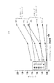
ここに記載するブロセスは、好適なプロセスチャンバーにおいて実施される。好適なプロセスチャンバーの例は、バッチ式炉及びシングルウエハリアクターを含む。例示のチャンバーは、放射的に加熱されたシングルウエハ、水平ガスフローリアクターである。このタイプの好適なリアクターは市販されており、そして、エーエスエム アメリカ、インク.(ASM America,Inc.)(フェニックス(Phoenix)、AZ)から市販されているシングルウエハエビタキシャルリアクターのイプシロン(Epsilon)(登録商標)シリーズを含む。図2は、米国特許出願公開2002/0173130(2002年11月21日発行)により詳細に記載されている(この全開示はこれよりここで参考文献として取り入れる)このようなリアクターを説明する。
堆積エピタキシャル層の質は、一般的に、堆積される基板のクリーンさ及び結晶クオリティーに左右される。基板表面は堆積層のテンプレートとして作用するため、基板表面の汚染物質は堆積層の質を落とす結果となる。多数のエピタキシャル堆積プロセスは、エピタキシャル堆積前に、酸素や炭素のような表面の汚染物質を取り除くために基板を加熱する、いわゆる「ベーク」工程を行う。
水素ベーク工程110、冷却工程120及び続く堆積工程の間、パージガスは、必要に応じて、リアクター壁に沿って流される。このパージガスフローは、基板表面から離れた汚染物質を除去するために、そして、ゲルマニウム膜の形成前または形成中の基板表面上における酸化生成物の形成を減少させるために設定される。該パージガスフローは、ガスの「シールド」でリアクターを効果的に覆い、そして、基板表面に接触する酸素及び水蒸気の量を減少させる。一つの実施形態において、該パージガスフローは、リアクター壁に沿った、高フローレートの高純度水素ガスを含む。好ましくは、該パージガスフローは、約5slmと約200slmの間で、さらに好ましくは約10slmと約150slmの間で、最も好ましくは約50slmと約100slmの間で供給される水素ガスを含む。水素はまた、ベーク工程110において、及び、他の工程中に、還元剤として有利に作用する。水素以外のパージガスは、多結晶堆積システムのような他の堆積システムにおいて、必要に応じて使用される。
上述するように、ゲルマニウム膜加工技術の一つの実施形態は、シード堆積130と共に始まる。図1に説明するように、該シード堆積130は、反応チャンバーが適切な温度に冷却されたとき、例えば冷却工程120の後に、開始される。例示の実施形態において、該シード堆積130は、堆積される物質のアイランド形成を減少または回避するために十分に低い温度で開始する。好ましくは、該シード堆積130は、約450℃より低くで開始する。他の実施形態において、該シード堆積工程130は、約350℃より低くで開始する。他の実施形態において、該シード堆積工程130は、約330℃で開始する。さらに好ましくは、該シード堆積工程130は、約330℃と約370℃の間で開始する。他の実施形態において、該シード堆積工程130は、約330℃と約450℃の間で開始する。一般的に、ゲルマニウム前駆体の熱的安定性が減少するにつれて、より低い堆積温度がさらにふさわしくなる傾向がある。該パージガスフローは、該シード堆積工程の間、必要に応じて続けられる。
図3に現在言及するように、ゲルマニウム膜の堆積は、温度ランプ140中において続く。例えば、一つの実施形態において、ゲルマニウム前駆体のフローレート及び堆積チャンバー内の圧力は、シード堆積130から続く。好ましくは、温度ランプ140中の堆積チャンバー内へのゲルマニウム前駆体のフローレートは、シード堆積130中のフローレートの約1%と約200%の間である。さらに好ましくは、温度ランプ140中の堆積チャンバー内へのゲルマニウム前駆体のフローレートは、シード堆積130中のフローレートの約10%と約100%の間である。最も好ましくは、温度ランプ140中の堆積チャンバー内へのゲルマニウム前駆体のフローレートは、シード堆積130中のフローレートの約50%と約100%の間である。例えば、ゲルマニウム膜の堆積は、ゲルマニウム前駆体のフローレートが実質的にシード堆積130と温度ランプ140の間で変化しない場合に実証された。
図1に説明するように、反応チャンバー中の温度が温度ランプ140中に増加した後、ゲルマニウム堆積は、バルク堆積150において続く。例示の実施形態において、ゲルマニウム堆積は、高温で及び実質的に一定の温度で続く。例示の実施形態において、バルク堆積150の間の堆積チャンバー中の圧力は、シード堆積130及び温度ランプ140の間の圧力と比較して実質的に変化しないままである。バルク堆積150の間の堆積されたゲルマニウム層は、あらかじめ堆積された厚みに応じて、通常緩和している。一つの実施形態において、ゲルマニウム層は、バルク堆積150の間、約500Å min−1と約900Å min−1の間の速度で成長する。他の実施形態において、ゲルマニウム層は、バルク堆積150の間、約500Å min−1と約700Å min−1の間の速度で成長する。バルク堆積150後、約50nmと約10μmの間の凝集体厚を有するゲルマニウム膜が生じる。他の実施形態において、約1μmと約2μmの間の凝集体厚を有するゲルマニウム膜が生じる。
必要に応じたポスト−アニール工程160は、バルク堆積150の後に行われる。アニーリングは、ゲルマニウム層の外側を滑らかにするよう転位することを有利に許容する。ポストアニール工程160の一つの実施形態において、該ゲルマニウム膜は、約930℃で、及び、約5分間大気圧に保たれる。ポストアニール工程160の他の実施形態において、熱サイクリングアニーリングプロセスが行われ、ここで、ゲルマニウム膜は、あらかじめ決定した時間、加熱と冷却が繰り返される。例示の実施形態において、ポストアニール工程160はスパイクアニールである。例えば、前述のイプシロン(Epsilon)(登録商標)リアクターにおいて、約950℃から約1150℃のピーク温度に到達するまで、200℃ sec−1と同じくらい早く温度を変化させることができる。たとえプラトーアニーリング(plateau annealing)を伴わなくとも、特定の実施形態において、このようなスパイクアニールは、特に高ゲルマニウム濃度を有する膜における欠陥を排除するのに十分である。例えば、これは、ここで開示した説明した「純粋な」ゲルマニウム膜のような、20%より高いゲルマニウム濃度を有する膜に特に適用でき、これはドープされたとドープされていないゲルマニウム膜の両方を含む。
ここで開示する技術の特定の実施形態は、エッチピット密度、表面粗さ、及び、膜厚を含む、有利な特性を有するゲルマニウム膜を生み出す。図面に含まれているものは、ここに開示の方法を使用して堆積させた例示のエッチピット装飾ゲルマニウム膜の表面スキャンである。この発明は理論に束縛されないが、ゲルマニウム膜、特に比較的薄い、及び/または、比較的高いゲルマニウム含量を有するゲルマニウム膜は、膜中の転位の滑面成長(gliding propagation)が急速に進められるメディウムを提供すると考えられる。例えば、Erich Kasper et al.に編集されたR. Hull, 「Metastable stained layer configuations in the SiGe/Si system」、 EMIS Datareviews, Series No. 24: Properties of SiGe and SiGe:C, INSPEC, 2000 (ロンドン UK)を参照する。この利点は、アニーリングが必要に応じて行われるにもかかわらず、ポスト−アニール工程を伴わなくとも得られ得る。
前述の詳細な記載は本発明の幾つかの実施形態を開示するが、この開示は単に説明的なものであり、また、本発明を限定していないと理解されるべきである。開示される特有の構成及び処理は上記記載のものと異なり、また、ここで記載した方法は、ゲルマニウム膜の堆積とは別の内容で使用され得ると認識すべきである。
Claims (17)
- 第一圧力で保持されている反応チャンバーにおいて、第一温度でシリコン含有表面上に純粋なゲルマニウムのシード層を堆積すること、
該シード層堆積後、純粋なゲルマニウムを堆積し続けながら該反応チャンバーの温度を上昇させること、及び
純粋なゲルマニウムを堆積し続けながら、第一温度より高い第二温度範囲であり、且つ第一圧力より低い第二圧力で、チャンバーを保持すること、
を含むゲルマニウム膜の形成方法。 - 該シード層が、1モノレイヤーと1000Åの間の厚みに堆積される、請求項1の方法。
- 該シード層が、3分未満の期間堆積される、請求項1の方法。
- 該堆積されたゲルマニウムが、3Å rms未満の表面粗さを有する、請求項1の方法。
- 該堆積されたゲルマニウムが、103cm−2未満のエッチピット密度を有する、請求項1の方法。
- 該反応チャンバーを通してパージガスを供給すること、ここで、
該パージガスはH2を含むこと、
該パージガスは、シード層の堆積中に、第一フローレートで該反応チャンバーを通過する流れを有すること、
該パージガスは、該反応チャンバーが第二温度範囲に保持される間、第二フローレートで該反応チャンバーを通して流れること、
及び
該第二フローレートは該第一フローレートより大きいこと、
をさらに含む請求項1の方法。 - 該シリコン含有表面から酸化生成物を除去するためにベーキングプロセスを行うこと、
該ベーキングプロセス後、及び、該シード層堆積前に、該シリコン含有表面を第一温度に冷却すること、及び
該シリコン含有表面を冷却している間に、該パージガスを、第一フローレートより大きい第三フローレートで反応チャンバーを通して流すこと、
をさらに含む、請求項6の方法。 - 該シリコン含有表面がミスカットを有する基板である、請求項1の方法。
- 該第二圧力が、第一圧力より90torrと50torrの間で低い、請求項1の方法。
- 該第二圧力が、第一圧力より80torrと60torrの間で低い、請求項1の方法。
- 該第二圧力が、10torrと40torrの間である、請求項1の方法。
- 該第一圧力が、100torrと10torrの間である、請求項1の方法。
- 該反応チャンバーが第二温度範囲に保持されている間に、塩素供給源を該反応チャンバーに供給することをさらに含む、請求項1に記載の方法。
- 該塩素供給源がHClである、請求項13の方法。
- 該塩素供給源がCl2である、請求項13の方法。
- 該塩素供給源がクロロゲルマンである、請求項13の方法。
- 該塩素供給源が、25sccmと200sccmの間のフローレートで該反応チャンバーに供給される、請求項13の方法。
Applications Claiming Priority (5)
| Application Number | Priority Date | Filing Date | Title |
|---|---|---|---|
| US54826904P | 2004-02-27 | 2004-02-27 | |
| US60/548,269 | 2004-02-27 | ||
| US55675204P | 2004-03-26 | 2004-03-26 | |
| US60/556,752 | 2004-03-26 | ||
| PCT/US2005/006150 WO2005084231A2 (en) | 2004-02-27 | 2005-02-25 | Germanium deposition |
Publications (2)
| Publication Number | Publication Date |
|---|---|
| JP2008501226A JP2008501226A (ja) | 2008-01-17 |
| JP4982355B2 true JP4982355B2 (ja) | 2012-07-25 |
Family
ID=34922680
Family Applications (1)
| Application Number | Title | Priority Date | Filing Date |
|---|---|---|---|
| JP2007501016A Active JP4982355B2 (ja) | 2004-02-27 | 2005-02-25 | ゲルマニウム膜の形成方法 |
Country Status (4)
| Country | Link |
|---|---|
| US (2) | US7329593B2 (ja) |
| EP (1) | EP1763893A2 (ja) |
| JP (1) | JP4982355B2 (ja) |
| WO (1) | WO2005084231A2 (ja) |
Families Citing this family (50)
| Publication number | Priority date | Publication date | Assignee | Title |
|---|---|---|---|---|
| US6274292B1 (en) * | 1998-02-25 | 2001-08-14 | Micron Technology, Inc. | Semiconductor processing methods |
| US7495313B2 (en) * | 2004-07-22 | 2009-02-24 | Board Of Trustees Of The Leland Stanford Junior University | Germanium substrate-type materials and approach therefor |
| US7678420B2 (en) * | 2005-06-22 | 2010-03-16 | Sandisk 3D Llc | Method of depositing germanium films |
| US20070154637A1 (en) * | 2005-12-19 | 2007-07-05 | Rohm And Haas Electronic Materials Llc | Organometallic composition |
| US7785995B2 (en) * | 2006-05-09 | 2010-08-31 | Asm America, Inc. | Semiconductor buffer structures |
| WO2007133837A2 (en) | 2006-05-12 | 2007-11-22 | Advanced Technology Materials, Inc. | Low temperature deposition of phase change memory materials |
| US7648853B2 (en) | 2006-07-11 | 2010-01-19 | Asm America, Inc. | Dual channel heterostructure |
| US7608526B2 (en) * | 2006-07-24 | 2009-10-27 | Asm America, Inc. | Strained layers within semiconductor buffer structures |
| KR20120118060A (ko) | 2006-11-02 | 2012-10-25 | 어드밴스드 테크놀러지 머티리얼즈, 인코포레이티드 | 금속 박막의 cvd/ald용으로 유용한 안티몬 및 게르마늄 착체 |
| WO2009084238A1 (ja) | 2007-12-28 | 2009-07-09 | Sumitomo Chemical Company, Limited | 半導体基板、半導体基板の製造方法および電子デバイス |
| CN101896998B (zh) | 2007-12-28 | 2013-03-27 | 住友化学株式会社 | 半导体基板、半导体基板的制造方法及电子器件 |
| CN101896999B (zh) | 2007-12-28 | 2012-08-08 | 住友化学株式会社 | 半导体基板、半导体基板的制造方法及电子器件 |
| US20090179160A1 (en) * | 2008-01-16 | 2009-07-16 | Semiconductor Energy Laboratory Co., Ltd. | Semiconductor substrate manufacturing apparatus |
| US20090215225A1 (en) | 2008-02-24 | 2009-08-27 | Advanced Technology Materials, Inc. | Tellurium compounds useful for deposition of tellurium containing materials |
| WO2009134989A2 (en) | 2008-05-02 | 2009-11-05 | Advanced Technology Materials, Inc. | Antimony compounds useful for deposition of antimony-containing materials |
| US8645123B2 (en) * | 2008-10-27 | 2014-02-04 | Microsoft Corporation | Image-based semantic distance |
| US8188512B2 (en) | 2008-12-03 | 2012-05-29 | Electronics And Telecommunications Research Institute | Growth of germanium epitaxial thin film with negative photoconductance characteristics and photodiode using the same |
| US9379011B2 (en) | 2008-12-19 | 2016-06-28 | Asm International N.V. | Methods for depositing nickel films and for making nickel silicide and nickel germanide |
| US7927942B2 (en) | 2008-12-19 | 2011-04-19 | Asm International N.V. | Selective silicide process |
| US20100183500A1 (en) * | 2009-01-17 | 2010-07-22 | Henry Lee | Germane gas production from germanium byproducts or impure germanium compounds |
| KR20160084491A (ko) | 2009-05-22 | 2016-07-13 | 엔테그리스, 아이엔씨. | 저온 gst 방법 |
| EP2275591B1 (en) * | 2009-07-10 | 2014-03-19 | Imec | Method for manufacturing a mono-crystalline layer of germanium or aluminium on a substrate |
| US9305779B2 (en) * | 2009-08-11 | 2016-04-05 | Bae Systems Information And Electronic Systems Integration Inc. | Method for growing germanium epitaxial films |
| KR101287196B1 (ko) * | 2009-12-03 | 2013-07-16 | 한국전자통신연구원 | 광 검출기 및 그 제조방법 |
| US8741394B2 (en) | 2010-03-25 | 2014-06-03 | Novellus Systems, Inc. | In-situ deposition of film stacks |
| KR101706809B1 (ko) | 2010-03-26 | 2017-02-15 | 엔테그리스, 아이엔씨. | 게르마늄 안티몬 텔루라이드 물질 및 이를 포함하는 장치 |
| US9190609B2 (en) | 2010-05-21 | 2015-11-17 | Entegris, Inc. | Germanium antimony telluride materials and devices incorporating same |
| JP5544343B2 (ja) * | 2010-10-29 | 2014-07-09 | 東京エレクトロン株式会社 | 成膜装置 |
| US8871617B2 (en) | 2011-04-22 | 2014-10-28 | Asm Ip Holding B.V. | Deposition and reduction of mixed metal oxide thin films |
| US8455292B2 (en) | 2011-09-09 | 2013-06-04 | International Business Machines Corporation | Deposition of germanium film |
| US9085045B2 (en) | 2011-11-04 | 2015-07-21 | Tokyo Electron Limited | Method and system for controlling a spike anneal process |
| US9093269B2 (en) | 2011-12-20 | 2015-07-28 | Asm America, Inc. | In-situ pre-clean prior to epitaxy |
| FR2984142B1 (fr) * | 2011-12-20 | 2013-12-20 | Oreal | Composition comprenant un polymere acrylique particulier et copolymere silicone, procede de traitement des fibres keratiniques le mettant en oeuvre |
| JP5780981B2 (ja) * | 2012-03-02 | 2015-09-16 | 東京エレクトロン株式会社 | ゲルマニウム薄膜の成膜方法 |
| US9127345B2 (en) | 2012-03-06 | 2015-09-08 | Asm America, Inc. | Methods for depositing an epitaxial silicon germanium layer having a germanium to silicon ratio greater than 1:1 using silylgermane and a diluent |
| US9165788B2 (en) | 2012-04-06 | 2015-10-20 | Novellus Systems, Inc. | Post-deposition soft annealing |
| KR102117124B1 (ko) | 2012-04-30 | 2020-05-29 | 엔테그리스, 아이엔씨. | 유전체 물질로 중심-충전된 상 변화 합금을 포함하는 상 변화 메모리 구조체 |
| US9117668B2 (en) * | 2012-05-23 | 2015-08-25 | Novellus Systems, Inc. | PECVD deposition of smooth silicon films |
| US20130334571A1 (en) * | 2012-06-19 | 2013-12-19 | International Business Machines Corporation | Epitaxial growth of smooth and highly strained germanium |
| US9388491B2 (en) | 2012-07-23 | 2016-07-12 | Novellus Systems, Inc. | Method for deposition of conformal films with catalysis assisted low temperature CVD |
| US9171715B2 (en) | 2012-09-05 | 2015-10-27 | Asm Ip Holding B.V. | Atomic layer deposition of GeO2 |
| WO2014070682A1 (en) | 2012-10-30 | 2014-05-08 | Advaned Technology Materials, Inc. | Double self-aligned phase change memory device structure |
| US9330899B2 (en) | 2012-11-01 | 2016-05-03 | Asm Ip Holding B.V. | Method of depositing thin film |
| US9275861B2 (en) | 2013-06-26 | 2016-03-01 | Globalfoundries Inc. | Methods of forming group III-V semiconductor materials on group IV substrates and the resulting substrate structures |
| US9218963B2 (en) | 2013-12-19 | 2015-12-22 | Asm Ip Holding B.V. | Cyclical deposition of germanium |
| JP6258813B2 (ja) | 2014-08-12 | 2018-01-10 | 東京エレクトロン株式会社 | ゲルマニウム膜の成膜方法および成膜装置 |
| TWI646581B (zh) * | 2015-02-09 | 2019-01-01 | 聯華電子股份有限公司 | 製作鍺磊晶層之方法以及應用其之製作元件之方法 |
| US9607842B1 (en) | 2015-10-02 | 2017-03-28 | Asm Ip Holding B.V. | Methods of forming metal silicides |
| CN110707006B (zh) * | 2018-07-09 | 2023-10-17 | 日升存储公司 | 锑掺杂的硅和硅锗膜的原位制备的方法 |
| JP7058575B2 (ja) | 2018-09-12 | 2022-04-22 | 株式会社Kokusai Electric | 半導体装置の製造方法、基板処理方法、基板処理装置、およびプログラム |
Family Cites Families (42)
| Publication number | Priority date | Publication date | Assignee | Title |
|---|---|---|---|---|
| US207127A (en) * | 1878-08-20 | Improvement in plaiting-machines | ||
| US124818A (en) * | 1872-03-19 | Improvement in hanging-baskets | ||
| US157787A (en) * | 1874-12-15 | Improvement in printing-telegraphs | ||
| US79692A (en) * | 1868-07-07 | scantlin | ||
| US82300A (en) * | 1868-09-22 | Improved oak-spring | ||
| US5221556A (en) * | 1987-06-24 | 1993-06-22 | Epsilon Technology, Inc. | Gas injectors for reaction chambers in CVD systems |
| JP3163267B2 (ja) * | 1991-03-20 | 2001-05-08 | 株式会社日立国際電気 | 気相成長方法 |
| US5259918A (en) * | 1991-06-12 | 1993-11-09 | International Business Machines Corporation | Heteroepitaxial growth of germanium on silicon by UHV/CVD |
| JPH05217921A (ja) * | 1991-09-13 | 1993-08-27 | Motorola Inc | 材料膜のエピタキシアル成長を行うための温度制御された処理 |
| JPH05326467A (ja) * | 1992-05-15 | 1993-12-10 | Toshiba Corp | 半導体基板及びその製造方法 |
| JP2759594B2 (ja) * | 1993-01-30 | 1998-05-28 | 信越半導体株式会社 | エピタキシャル基板の製造方法 |
| US6093252A (en) * | 1995-08-03 | 2000-07-25 | Asm America, Inc. | Process chamber with inner support |
| JP2954039B2 (ja) * | 1996-09-05 | 1999-09-27 | 日本電気株式会社 | SiGe薄膜の成膜方法 |
| JP2953567B2 (ja) | 1997-02-06 | 1999-09-27 | 日本電気株式会社 | 半導体装置の製造方法 |
| KR100400808B1 (ko) * | 1997-06-24 | 2003-10-08 | 매사츄세츠 인스티튜트 오브 테크놀러지 | 그레이드된 GeSi층 및 평탄화를 사용한 Si상의 Ge의 쓰레딩 전위 밀도 제어 |
| FR2773177B1 (fr) * | 1997-12-29 | 2000-03-17 | France Telecom | Procede d'obtention d'une couche de germanium ou silicium monocristallin sur un substrat de silicium ou germanium monocristallin, respectivement, et produits multicouches obtenus |
| FR2783254B1 (fr) | 1998-09-10 | 2000-11-10 | France Telecom | Procede d'obtention d'une couche de germanium monocristallin sur un substrat de silicium monocristallin,et produits obtenus |
| US6319782B1 (en) * | 1998-09-10 | 2001-11-20 | Matsushita Electric Industrial Co., Ltd. | Semiconductor device and method of fabricating the same |
| US6635110B1 (en) * | 1999-06-25 | 2003-10-21 | Massachusetts Institute Of Technology | Cyclic thermal anneal for dislocation reduction |
| US6373112B1 (en) * | 1999-12-02 | 2002-04-16 | Intel Corporation | Polysilicon-germanium MOSFET gate electrodes |
| WO2001041544A2 (en) | 1999-12-11 | 2001-06-14 | Asm America, Inc. | Deposition of gate stacks including silicon germanium layers |
| US6633066B1 (en) | 2000-01-07 | 2003-10-14 | Samsung Electronics Co., Ltd. | CMOS integrated circuit devices and substrates having unstrained silicon active layers |
| JP4406995B2 (ja) | 2000-03-27 | 2010-02-03 | パナソニック株式会社 | 半導体基板および半導体基板の製造方法 |
| DE10025871A1 (de) * | 2000-05-25 | 2001-12-06 | Wacker Siltronic Halbleitermat | Epitaxierte Halbleiterscheibe und Verfahren zu ihrer Herstellung |
| US6592942B1 (en) * | 2000-07-07 | 2003-07-15 | Asm International N.V. | Method for vapour deposition of a film onto a substrate |
| JP2002093735A (ja) * | 2000-09-13 | 2002-03-29 | Sony Corp | 半導体装置の製造方法 |
| KR101050377B1 (ko) | 2001-02-12 | 2011-07-20 | 에이에스엠 아메리카, 인코포레이티드 | 반도체 박막 증착을 위한 개선된 공정 |
| US7026219B2 (en) * | 2001-02-12 | 2006-04-11 | Asm America, Inc. | Integration of high k gate dielectric |
| JP3660897B2 (ja) * | 2001-09-03 | 2005-06-15 | 株式会社ルネサステクノロジ | 半導体装置の製造方法 |
| US6875279B2 (en) * | 2001-11-16 | 2005-04-05 | International Business Machines Corporation | Single reactor, multi-pressure chemical vapor deposition for semiconductor devices |
| US20030124818A1 (en) | 2001-12-28 | 2003-07-03 | Applied Materials, Inc. | Method and apparatus for forming silicon containing films |
| US6723622B2 (en) | 2002-02-21 | 2004-04-20 | Intel Corporation | Method of forming a germanium film on a semiconductor substrate that includes the formation of a graded silicon-germanium buffer layer prior to the formation of a germanium layer |
| US6864520B2 (en) * | 2002-04-04 | 2005-03-08 | International Business Machines Corporation | Germanium field effect transistor and method of fabricating the same |
| KR20050032527A (ko) * | 2002-06-19 | 2005-04-07 | 메사추세츠 인스티튜트 오브 테크놀로지 | 게르마늄 광검출기 |
| US6887773B2 (en) * | 2002-06-19 | 2005-05-03 | Luxtera, Inc. | Methods of incorporating germanium within CMOS process |
| US7238595B2 (en) * | 2003-03-13 | 2007-07-03 | Asm America, Inc. | Epitaxial semiconductor deposition methods and structures |
| US20050067377A1 (en) * | 2003-09-25 | 2005-03-31 | Ryan Lei | Germanium-on-insulator fabrication utilizing wafer bonding |
| US7132338B2 (en) | 2003-10-10 | 2006-11-07 | Applied Materials, Inc. | Methods to fabricate MOSFET devices using selective deposition process |
| US7199021B2 (en) * | 2004-06-22 | 2007-04-03 | Texas Instruments Incorporated | Methods and systems to mitigate etch stop clipping for shallow trench isolation fabrication |
| US7037856B1 (en) * | 2005-06-10 | 2006-05-02 | Sharp Laboratories Of America, Inc. | Method of fabricating a low-defect strained epitaxial germanium film on silicon |
| KR100641063B1 (ko) * | 2005-08-26 | 2006-11-01 | 삼성전자주식회사 | 단결정 구조물 형성 방법 및 이를 이용한 반도체 장치의제조 방법 |
| JP4786495B2 (ja) * | 2005-11-24 | 2011-10-05 | 東京エレクトロン株式会社 | 薄膜形成装置の洗浄方法、薄膜形成方法、薄膜形成装置及びプログラム |
-
2005
- 2005-02-25 WO PCT/US2005/006150 patent/WO2005084231A2/en active Application Filing
- 2005-02-25 US US11/067,307 patent/US7329593B2/en active Active
- 2005-02-25 JP JP2007501016A patent/JP4982355B2/ja active Active
- 2005-02-25 EP EP05723841A patent/EP1763893A2/en not_active Withdrawn
-
2007
- 2007-10-04 US US11/867,318 patent/US7479443B2/en active Active
Also Published As
| Publication number | Publication date |
|---|---|
| US20080017101A1 (en) | 2008-01-24 |
| WO2005084231A3 (en) | 2009-06-25 |
| US7329593B2 (en) | 2008-02-12 |
| EP1763893A2 (en) | 2007-03-21 |
| US20050191826A1 (en) | 2005-09-01 |
| WO2005084231A2 (en) | 2005-09-15 |
| US7479443B2 (en) | 2009-01-20 |
| JP2008501226A (ja) | 2008-01-17 |
Similar Documents
| Publication | Publication Date | Title |
|---|---|---|
| JP4982355B2 (ja) | ゲルマニウム膜の形成方法 | |
| US7238595B2 (en) | Epitaxial semiconductor deposition methods and structures | |
| US7682947B2 (en) | Epitaxial semiconductor deposition methods and structures | |
| US7396743B2 (en) | Low temperature epitaxial growth of silicon-containing films using UV radiation | |
| KR100870507B1 (ko) | 트리실란을 사용한, 혼합 기판상의 증착 | |
| TWI385714B (zh) | 含矽薄膜的選擇性沉積 | |
| US6749687B1 (en) | In situ growth of oxide and silicon layers | |
| KR20130044312A (ko) | 시클로헥사실란을 이용한 박막 및 이의 제조방법 | |
| KR20090015138A (ko) | 클로로폴리실란들을 이용한 실리콘-포함 막들의 선택적 증착 방법들 및 시스템들 | |
| US8409350B2 (en) | Gallium nitride crystal growth method, gallium nitride crystal substrate, epi-wafer manufacturing method, and epi-wafer | |
| US20180209063A1 (en) | Growing epitaxial 3c-sic on single-crystal silicon | |
| US7029995B2 (en) | Methods for depositing amorphous materials and using them as templates for epitaxial films by solid phase epitaxy | |
| JP4782670B2 (ja) | エピタキシャルGe含有膜の成長方法及びエピタキシャル半導体成膜システム | |
| JP2002539327A (ja) | 基板表面への金属酸化物の化学的気相成長法による成膜方法および装置 | |
| EP1887617B1 (en) | Deposition method over mixed substrates using trisilane | |
| Lin | Low-temperature halo-carbon homoepitaxial growth of 4H-silicon carbide |
Legal Events
| Date | Code | Title | Description |
|---|---|---|---|
| A621 | Written request for application examination |
Free format text: JAPANESE INTERMEDIATE CODE: A621 Effective date: 20080205 |
|
| RD02 | Notification of acceptance of power of attorney |
Free format text: JAPANESE INTERMEDIATE CODE: A7422 Effective date: 20090807 |
|
| RD03 | Notification of appointment of power of attorney |
Free format text: JAPANESE INTERMEDIATE CODE: A7423 Effective date: 20090807 |
|
| A521 | Request for written amendment filed |
Free format text: JAPANESE INTERMEDIATE CODE: A821 Effective date: 20091207 |
|
| RD04 | Notification of resignation of power of attorney |
Free format text: JAPANESE INTERMEDIATE CODE: A7424 Effective date: 20091207 |
|
| A977 | Report on retrieval |
Free format text: JAPANESE INTERMEDIATE CODE: A971007 Effective date: 20101130 |
|
| A131 | Notification of reasons for refusal |
Free format text: JAPANESE INTERMEDIATE CODE: A131 Effective date: 20101214 |
|
| A601 | Written request for extension of time |
Free format text: JAPANESE INTERMEDIATE CODE: A601 Effective date: 20110314 |
|
| A602 | Written permission of extension of time |
Free format text: JAPANESE INTERMEDIATE CODE: A602 Effective date: 20110322 |
|
| A521 | Request for written amendment filed |
Free format text: JAPANESE INTERMEDIATE CODE: A523 Effective date: 20110412 |
|
| A131 | Notification of reasons for refusal |
Free format text: JAPANESE INTERMEDIATE CODE: A131 Effective date: 20111220 |
|
| A521 | Request for written amendment filed |
Free format text: JAPANESE INTERMEDIATE CODE: A523 Effective date: 20120309 |
|
| TRDD | Decision of grant or rejection written | ||
| A01 | Written decision to grant a patent or to grant a registration (utility model) |
Free format text: JAPANESE INTERMEDIATE CODE: A01 Effective date: 20120410 |
|
| A01 | Written decision to grant a patent or to grant a registration (utility model) |
Free format text: JAPANESE INTERMEDIATE CODE: A01 |
|
| A61 | First payment of annual fees (during grant procedure) |
Free format text: JAPANESE INTERMEDIATE CODE: A61 Effective date: 20120423 |
|
| FPAY | Renewal fee payment (event date is renewal date of database) |
Free format text: PAYMENT UNTIL: 20150427 Year of fee payment: 3 |
|
| R150 | Certificate of patent or registration of utility model |
Ref document number: 4982355 Country of ref document: JP Free format text: JAPANESE INTERMEDIATE CODE: R150 Free format text: JAPANESE INTERMEDIATE CODE: R150 |
|
| R250 | Receipt of annual fees |
Free format text: JAPANESE INTERMEDIATE CODE: R250 |
|
| R250 | Receipt of annual fees |
Free format text: JAPANESE INTERMEDIATE CODE: R250 |
|
| R250 | Receipt of annual fees |
Free format text: JAPANESE INTERMEDIATE CODE: R250 |
|
| R250 | Receipt of annual fees |
Free format text: JAPANESE INTERMEDIATE CODE: R250 |
|
| R250 | Receipt of annual fees |
Free format text: JAPANESE INTERMEDIATE CODE: R250 |
|
| R250 | Receipt of annual fees |
Free format text: JAPANESE INTERMEDIATE CODE: R250 |
|
| R250 | Receipt of annual fees |
Free format text: JAPANESE INTERMEDIATE CODE: R250 |
|
| S111 | Request for change of ownership or part of ownership |
Free format text: JAPANESE INTERMEDIATE CODE: R313113 |
|
| R350 | Written notification of registration of transfer |
Free format text: JAPANESE INTERMEDIATE CODE: R350 |
|
| R250 | Receipt of annual fees |
Free format text: JAPANESE INTERMEDIATE CODE: R250 |
|
| R250 | Receipt of annual fees |
Free format text: JAPANESE INTERMEDIATE CODE: R250 |