JP4979587B2 - ゲート及びチャネル内に歪を誘起させてcmosトランジスタの性能を向上させる方法 - Google Patents
ゲート及びチャネル内に歪を誘起させてcmosトランジスタの性能を向上させる方法 Download PDFInfo
- Publication number
- JP4979587B2 JP4979587B2 JP2007541381A JP2007541381A JP4979587B2 JP 4979587 B2 JP4979587 B2 JP 4979587B2 JP 2007541381 A JP2007541381 A JP 2007541381A JP 2007541381 A JP2007541381 A JP 2007541381A JP 4979587 B2 JP4979587 B2 JP 4979587B2
- Authority
- JP
- Japan
- Prior art keywords
- nfet
- pfet
- hard layer
- gate stack
- gate
- Prior art date
- Legal status (The legal status is an assumption and is not a legal conclusion. Google has not performed a legal analysis and makes no representation as to the accuracy of the status listed.)
- Expired - Fee Related
Links
- 238000000034 method Methods 0.000 title claims description 40
- 230000001939 inductive effect Effects 0.000 title description 2
- 238000004519 manufacturing process Methods 0.000 claims description 22
- 229910021420 polycrystalline silicon Inorganic materials 0.000 claims description 17
- 229920005591 polysilicon Polymers 0.000 claims description 16
- 238000010438 heat treatment Methods 0.000 claims description 14
- 229910052581 Si3N4 Inorganic materials 0.000 claims description 13
- HQVNEWCFYHHQES-UHFFFAOYSA-N silicon nitride Chemical compound N12[Si]34N5[Si]62N3[Si]51N64 HQVNEWCFYHHQES-UHFFFAOYSA-N 0.000 claims description 13
- 229910021417 amorphous silicon Inorganic materials 0.000 claims description 8
- 150000002500 ions Chemical class 0.000 claims description 7
- 239000000758 substrate Substances 0.000 claims description 7
- 238000005468 ion implantation Methods 0.000 claims description 5
- 238000002425 crystallisation Methods 0.000 claims description 4
- 230000008025 crystallization Effects 0.000 claims description 4
- HBMJWWWQQXIZIP-UHFFFAOYSA-N silicon carbide Chemical compound [Si+]#[C-] HBMJWWWQQXIZIP-UHFFFAOYSA-N 0.000 claims description 4
- 229910010271 silicon carbide Inorganic materials 0.000 claims description 4
- 238000005280 amorphization Methods 0.000 claims 3
- 238000000059 patterning Methods 0.000 claims 1
- 230000005669 field effect Effects 0.000 description 17
- 238000000137 annealing Methods 0.000 description 15
- 239000000463 material Substances 0.000 description 13
- 229910044991 metal oxide Inorganic materials 0.000 description 12
- 150000004706 metal oxides Chemical class 0.000 description 12
- 239000004065 semiconductor Substances 0.000 description 12
- 239000004020 conductor Substances 0.000 description 10
- 125000006850 spacer group Chemical group 0.000 description 5
- 229920002120 photoresistant polymer Polymers 0.000 description 4
- 239000007943 implant Substances 0.000 description 3
- 238000002513 implantation Methods 0.000 description 3
- 229910021332 silicide Inorganic materials 0.000 description 3
- FVBUAEGBCNSCDD-UHFFFAOYSA-N silicide(4-) Chemical group [Si-4] FVBUAEGBCNSCDD-UHFFFAOYSA-N 0.000 description 3
- 238000005229 chemical vapour deposition Methods 0.000 description 2
- 230000000295 complement effect Effects 0.000 description 2
- 239000002019 doping agent Substances 0.000 description 2
- 238000005530 etching Methods 0.000 description 2
- 238000002955 isolation Methods 0.000 description 2
- 230000000873 masking effect Effects 0.000 description 2
- 238000004151 rapid thermal annealing Methods 0.000 description 2
- 229910004298 SiO 2 Inorganic materials 0.000 description 1
- XUIMIQQOPSSXEZ-UHFFFAOYSA-N Silicon Chemical compound [Si] XUIMIQQOPSSXEZ-UHFFFAOYSA-N 0.000 description 1
- 238000005452 bending Methods 0.000 description 1
- 238000004140 cleaning Methods 0.000 description 1
- 229910021419 crystalline silicon Inorganic materials 0.000 description 1
- 230000000593 degrading effect Effects 0.000 description 1
- 238000005137 deposition process Methods 0.000 description 1
- 230000000694 effects Effects 0.000 description 1
- 230000005684 electric field Effects 0.000 description 1
- 125000001475 halogen functional group Chemical group 0.000 description 1
- 238000010849 ion bombardment Methods 0.000 description 1
- 239000002184 metal Substances 0.000 description 1
- 230000004048 modification Effects 0.000 description 1
- 238000012986 modification Methods 0.000 description 1
- 150000004767 nitrides Chemical class 0.000 description 1
- 239000002245 particle Substances 0.000 description 1
- 238000000623 plasma-assisted chemical vapour deposition Methods 0.000 description 1
- 229910052710 silicon Inorganic materials 0.000 description 1
- 239000010703 silicon Substances 0.000 description 1
- 239000000126 substance Substances 0.000 description 1
Images


Classifications
-
- H—ELECTRICITY
- H01—ELECTRIC ELEMENTS
- H01L—SEMICONDUCTOR DEVICES NOT COVERED BY CLASS H10
- H01L21/00—Processes or apparatus adapted for the manufacture or treatment of semiconductor or solid state devices or of parts thereof
- H01L21/70—Manufacture or treatment of devices consisting of a plurality of solid state components formed in or on a common substrate or of parts thereof; Manufacture of integrated circuit devices or of parts thereof
- H01L21/77—Manufacture or treatment of devices consisting of a plurality of solid state components or integrated circuits formed in, or on, a common substrate
- H01L21/78—Manufacture or treatment of devices consisting of a plurality of solid state components or integrated circuits formed in, or on, a common substrate with subsequent division of the substrate into plural individual devices
- H01L21/82—Manufacture or treatment of devices consisting of a plurality of solid state components or integrated circuits formed in, or on, a common substrate with subsequent division of the substrate into plural individual devices to produce devices, e.g. integrated circuits, each consisting of a plurality of components
- H01L21/822—Manufacture or treatment of devices consisting of a plurality of solid state components or integrated circuits formed in, or on, a common substrate with subsequent division of the substrate into plural individual devices to produce devices, e.g. integrated circuits, each consisting of a plurality of components the substrate being a semiconductor, using silicon technology
- H01L21/8232—Field-effect technology
- H01L21/8234—MIS technology, i.e. integration processes of field effect transistors of the conductor-insulator-semiconductor type
- H01L21/8238—Complementary field-effect transistors, e.g. CMOS
- H01L21/823807—Complementary field-effect transistors, e.g. CMOS with a particular manufacturing method of the channel structures, e.g. channel implants, halo or pocket implants, or channel materials
-
- H—ELECTRICITY
- H01—ELECTRIC ELEMENTS
- H01L—SEMICONDUCTOR DEVICES NOT COVERED BY CLASS H10
- H01L21/00—Processes or apparatus adapted for the manufacture or treatment of semiconductor or solid state devices or of parts thereof
- H01L21/70—Manufacture or treatment of devices consisting of a plurality of solid state components formed in or on a common substrate or of parts thereof; Manufacture of integrated circuit devices or of parts thereof
- H01L21/77—Manufacture or treatment of devices consisting of a plurality of solid state components or integrated circuits formed in, or on, a common substrate
- H01L21/78—Manufacture or treatment of devices consisting of a plurality of solid state components or integrated circuits formed in, or on, a common substrate with subsequent division of the substrate into plural individual devices
- H01L21/82—Manufacture or treatment of devices consisting of a plurality of solid state components or integrated circuits formed in, or on, a common substrate with subsequent division of the substrate into plural individual devices to produce devices, e.g. integrated circuits, each consisting of a plurality of components
- H01L21/822—Manufacture or treatment of devices consisting of a plurality of solid state components or integrated circuits formed in, or on, a common substrate with subsequent division of the substrate into plural individual devices to produce devices, e.g. integrated circuits, each consisting of a plurality of components the substrate being a semiconductor, using silicon technology
- H01L21/8232—Field-effect technology
- H01L21/8234—MIS technology, i.e. integration processes of field effect transistors of the conductor-insulator-semiconductor type
- H01L21/8238—Complementary field-effect transistors, e.g. CMOS
- H01L21/823828—Complementary field-effect transistors, e.g. CMOS with a particular manufacturing method of the gate conductors, e.g. particular materials, shapes
- H01L21/823835—Complementary field-effect transistors, e.g. CMOS with a particular manufacturing method of the gate conductors, e.g. particular materials, shapes silicided or salicided gate conductors
-
- H—ELECTRICITY
- H01—ELECTRIC ELEMENTS
- H01L—SEMICONDUCTOR DEVICES NOT COVERED BY CLASS H10
- H01L21/00—Processes or apparatus adapted for the manufacture or treatment of semiconductor or solid state devices or of parts thereof
- H01L21/70—Manufacture or treatment of devices consisting of a plurality of solid state components formed in or on a common substrate or of parts thereof; Manufacture of integrated circuit devices or of parts thereof
- H01L21/77—Manufacture or treatment of devices consisting of a plurality of solid state components or integrated circuits formed in, or on, a common substrate
- H01L21/78—Manufacture or treatment of devices consisting of a plurality of solid state components or integrated circuits formed in, or on, a common substrate with subsequent division of the substrate into plural individual devices
- H01L21/82—Manufacture or treatment of devices consisting of a plurality of solid state components or integrated circuits formed in, or on, a common substrate with subsequent division of the substrate into plural individual devices to produce devices, e.g. integrated circuits, each consisting of a plurality of components
- H01L21/822—Manufacture or treatment of devices consisting of a plurality of solid state components or integrated circuits formed in, or on, a common substrate with subsequent division of the substrate into plural individual devices to produce devices, e.g. integrated circuits, each consisting of a plurality of components the substrate being a semiconductor, using silicon technology
- H01L21/8232—Field-effect technology
- H01L21/8234—MIS technology, i.e. integration processes of field effect transistors of the conductor-insulator-semiconductor type
- H01L21/8238—Complementary field-effect transistors, e.g. CMOS
- H01L21/823828—Complementary field-effect transistors, e.g. CMOS with a particular manufacturing method of the gate conductors, e.g. particular materials, shapes
- H01L21/823842—Complementary field-effect transistors, e.g. CMOS with a particular manufacturing method of the gate conductors, e.g. particular materials, shapes gate conductors with different gate conductor materials or different gate conductor implants, e.g. dual gate structures
-
- H—ELECTRICITY
- H01—ELECTRIC ELEMENTS
- H01L—SEMICONDUCTOR DEVICES NOT COVERED BY CLASS H10
- H01L21/00—Processes or apparatus adapted for the manufacture or treatment of semiconductor or solid state devices or of parts thereof
- H01L21/70—Manufacture or treatment of devices consisting of a plurality of solid state components formed in or on a common substrate or of parts thereof; Manufacture of integrated circuit devices or of parts thereof
- H01L21/77—Manufacture or treatment of devices consisting of a plurality of solid state components or integrated circuits formed in, or on, a common substrate
- H01L21/78—Manufacture or treatment of devices consisting of a plurality of solid state components or integrated circuits formed in, or on, a common substrate with subsequent division of the substrate into plural individual devices
- H01L21/82—Manufacture or treatment of devices consisting of a plurality of solid state components or integrated circuits formed in, or on, a common substrate with subsequent division of the substrate into plural individual devices to produce devices, e.g. integrated circuits, each consisting of a plurality of components
- H01L21/822—Manufacture or treatment of devices consisting of a plurality of solid state components or integrated circuits formed in, or on, a common substrate with subsequent division of the substrate into plural individual devices to produce devices, e.g. integrated circuits, each consisting of a plurality of components the substrate being a semiconductor, using silicon technology
- H01L21/8232—Field-effect technology
- H01L21/8234—MIS technology, i.e. integration processes of field effect transistors of the conductor-insulator-semiconductor type
- H01L21/8238—Complementary field-effect transistors, e.g. CMOS
- H01L21/823864—Complementary field-effect transistors, e.g. CMOS with a particular manufacturing method of the gate sidewall spacers, e.g. double spacers, particular spacer material or shape
-
- H—ELECTRICITY
- H01—ELECTRIC ELEMENTS
- H01L—SEMICONDUCTOR DEVICES NOT COVERED BY CLASS H10
- H01L29/00—Semiconductor devices adapted for rectifying, amplifying, oscillating or switching, or capacitors or resistors with at least one potential-jump barrier or surface barrier, e.g. PN junction depletion layer or carrier concentration layer; Details of semiconductor bodies or of electrodes thereof ; Multistep manufacturing processes therefor
- H01L29/66—Types of semiconductor device ; Multistep manufacturing processes therefor
- H01L29/68—Types of semiconductor device ; Multistep manufacturing processes therefor controllable by only the electric current supplied, or only the electric potential applied, to an electrode which does not carry the current to be rectified, amplified or switched
- H01L29/76—Unipolar devices, e.g. field effect transistors
- H01L29/772—Field effect transistors
- H01L29/78—Field effect transistors with field effect produced by an insulated gate
- H01L29/7842—Field effect transistors with field effect produced by an insulated gate means for exerting mechanical stress on the crystal lattice of the channel region, e.g. using a flexible substrate
- H01L29/7843—Field effect transistors with field effect produced by an insulated gate means for exerting mechanical stress on the crystal lattice of the channel region, e.g. using a flexible substrate the means being an applied insulating layer
-
- H—ELECTRICITY
- H01—ELECTRIC ELEMENTS
- H01L—SEMICONDUCTOR DEVICES NOT COVERED BY CLASS H10
- H01L29/00—Semiconductor devices adapted for rectifying, amplifying, oscillating or switching, or capacitors or resistors with at least one potential-jump barrier or surface barrier, e.g. PN junction depletion layer or carrier concentration layer; Details of semiconductor bodies or of electrodes thereof ; Multistep manufacturing processes therefor
- H01L29/66—Types of semiconductor device ; Multistep manufacturing processes therefor
- H01L29/68—Types of semiconductor device ; Multistep manufacturing processes therefor controllable by only the electric current supplied, or only the electric potential applied, to an electrode which does not carry the current to be rectified, amplified or switched
- H01L29/76—Unipolar devices, e.g. field effect transistors
- H01L29/772—Field effect transistors
- H01L29/78—Field effect transistors with field effect produced by an insulated gate
- H01L29/7842—Field effect transistors with field effect produced by an insulated gate means for exerting mechanical stress on the crystal lattice of the channel region, e.g. using a flexible substrate
- H01L29/7845—Field effect transistors with field effect produced by an insulated gate means for exerting mechanical stress on the crystal lattice of the channel region, e.g. using a flexible substrate the means being a conductive material, e.g. silicided S/D or Gate
-
- H—ELECTRICITY
- H01—ELECTRIC ELEMENTS
- H01L—SEMICONDUCTOR DEVICES NOT COVERED BY CLASS H10
- H01L29/00—Semiconductor devices adapted for rectifying, amplifying, oscillating or switching, or capacitors or resistors with at least one potential-jump barrier or surface barrier, e.g. PN junction depletion layer or carrier concentration layer; Details of semiconductor bodies or of electrodes thereof ; Multistep manufacturing processes therefor
- H01L29/66—Types of semiconductor device ; Multistep manufacturing processes therefor
- H01L29/68—Types of semiconductor device ; Multistep manufacturing processes therefor controllable by only the electric current supplied, or only the electric potential applied, to an electrode which does not carry the current to be rectified, amplified or switched
- H01L29/76—Unipolar devices, e.g. field effect transistors
- H01L29/772—Field effect transistors
- H01L29/78—Field effect transistors with field effect produced by an insulated gate
- H01L29/7842—Field effect transistors with field effect produced by an insulated gate means for exerting mechanical stress on the crystal lattice of the channel region, e.g. using a flexible substrate
- H01L29/7847—Field effect transistors with field effect produced by an insulated gate means for exerting mechanical stress on the crystal lattice of the channel region, e.g. using a flexible substrate using a memorization technique, e.g. re-crystallization under strain, bonding on a substrate having a thermal expansion coefficient different from the one of the region
-
- H—ELECTRICITY
- H01—ELECTRIC ELEMENTS
- H01L—SEMICONDUCTOR DEVICES NOT COVERED BY CLASS H10
- H01L29/00—Semiconductor devices adapted for rectifying, amplifying, oscillating or switching, or capacitors or resistors with at least one potential-jump barrier or surface barrier, e.g. PN junction depletion layer or carrier concentration layer; Details of semiconductor bodies or of electrodes thereof ; Multistep manufacturing processes therefor
- H01L29/66—Types of semiconductor device ; Multistep manufacturing processes therefor
- H01L29/66007—Multistep manufacturing processes
- H01L29/66075—Multistep manufacturing processes of devices having semiconductor bodies comprising group 14 or group 13/15 materials
- H01L29/66227—Multistep manufacturing processes of devices having semiconductor bodies comprising group 14 or group 13/15 materials the devices being controllable only by the electric current supplied or the electric potential applied, to an electrode which does not carry the current to be rectified, amplified or switched, e.g. three-terminal devices
- H01L29/66409—Unipolar field-effect transistors
- H01L29/66477—Unipolar field-effect transistors with an insulated gate, i.e. MISFET
- H01L29/665—Unipolar field-effect transistors with an insulated gate, i.e. MISFET using self aligned silicidation, i.e. salicide
-
- H—ELECTRICITY
- H01—ELECTRIC ELEMENTS
- H01L—SEMICONDUCTOR DEVICES NOT COVERED BY CLASS H10
- H01L29/00—Semiconductor devices adapted for rectifying, amplifying, oscillating or switching, or capacitors or resistors with at least one potential-jump barrier or surface barrier, e.g. PN junction depletion layer or carrier concentration layer; Details of semiconductor bodies or of electrodes thereof ; Multistep manufacturing processes therefor
- H01L29/66—Types of semiconductor device ; Multistep manufacturing processes therefor
- H01L29/66007—Multistep manufacturing processes
- H01L29/66075—Multistep manufacturing processes of devices having semiconductor bodies comprising group 14 or group 13/15 materials
- H01L29/66227—Multistep manufacturing processes of devices having semiconductor bodies comprising group 14 or group 13/15 materials the devices being controllable only by the electric current supplied or the electric potential applied, to an electrode which does not carry the current to be rectified, amplified or switched, e.g. three-terminal devices
- H01L29/66409—Unipolar field-effect transistors
- H01L29/66477—Unipolar field-effect transistors with an insulated gate, i.e. MISFET
- H01L29/66545—Unipolar field-effect transistors with an insulated gate, i.e. MISFET using a dummy, i.e. replacement gate in a process wherein at least a part of the final gate is self aligned to the dummy gate
-
- H—ELECTRICITY
- H01—ELECTRIC ELEMENTS
- H01L—SEMICONDUCTOR DEVICES NOT COVERED BY CLASS H10
- H01L29/00—Semiconductor devices adapted for rectifying, amplifying, oscillating or switching, or capacitors or resistors with at least one potential-jump barrier or surface barrier, e.g. PN junction depletion layer or carrier concentration layer; Details of semiconductor bodies or of electrodes thereof ; Multistep manufacturing processes therefor
- H01L29/66—Types of semiconductor device ; Multistep manufacturing processes therefor
- H01L29/66007—Multistep manufacturing processes
- H01L29/66075—Multistep manufacturing processes of devices having semiconductor bodies comprising group 14 or group 13/15 materials
- H01L29/66227—Multistep manufacturing processes of devices having semiconductor bodies comprising group 14 or group 13/15 materials the devices being controllable only by the electric current supplied or the electric potential applied, to an electrode which does not carry the current to be rectified, amplified or switched, e.g. three-terminal devices
- H01L29/66409—Unipolar field-effect transistors
- H01L29/66477—Unipolar field-effect transistors with an insulated gate, i.e. MISFET
- H01L29/6656—Unipolar field-effect transistors with an insulated gate, i.e. MISFET using multiple spacer layers, e.g. multiple sidewall spacers
Description
本発明のこれら及びその他の態様を以下でさらに詳細に説明する。
本発明は好ましい実施形態に関して説明されたが、当業者は、本発明が添付の特許請求の範囲の精神及び範囲内の変更を実施できることを認識する。
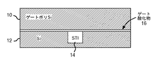
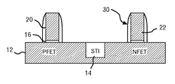
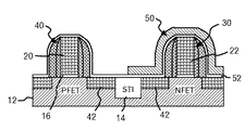
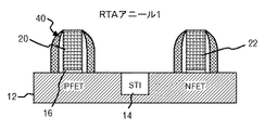
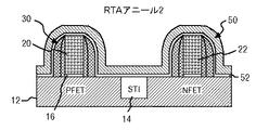
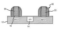
14:浅いトレンチ分離(STI)領域
16:ゲート酸化物
20:ゲート
22:ゲート
40:側壁スペーサ
65:シリサイド領域
70:引張応力
Claims (13)
- CMOSトランジスタを製造する方法であって、
ポリシリコンを含むゲートスタックを有するNFETおよびPFETを基板上に形成するステップと、
前記ゲートスタックのポリシリコンをアモルファス化するステップと、
前記アモルファス化後の前記NFETのみを硬質層で覆うステップと、
前記NFETおよび前記PFETを加熱して、前記PFETのチャネル領域内に引張応力を生じさせることなく、前記硬質層で覆われた前記NFETのチャネル領域内に引張応力を生じさせるステップと、を含む方法。 - 前記硬質層で覆うステップの前に、前記NFET上に酸化物層を形成するステップをさらに含む、請求項1に記載の方法。
- 前記アモルファス化するステップは、前記ゲートスタックにイオンを注入するステップを含む、請求項1に記載の方法。
- 前記加熱ステップの間、前記硬質層で覆われた前記NFETのゲートスタックの結果として前記NFETの前記ゲートスタック内に圧縮応力を生じさせ、当該圧縮応力が前記NFETのチャネル領域内に引張応力を生じさせる、請求項1に記載の方法。
- 前記NFETのゲートスタックの体積膨張は、前記ポリシリコンのアモルファス化により生成されたアモルファスシリコンの結晶化により生ずる、請求項4に記載の方法。
- 前記硬質層は、窒化ケイ素または炭化ケイ素を含む、請求項1に記載の方法。
- 前記NFETのみを硬質層で覆うステップは、
前記NFETおよび前記PFETを硬質層で覆うステップと、
前記硬質層の一部をパターン形成して、前記硬質層を前記NFET上にのみ残すステップと、を含む請求項1に記載の方法。 - CMOSトランジスタの製造方法であって、
ポリシリコンを含むゲートスタックを有するNFETおよびPFETを基板上に形成するステップと、
前記PFETをマスクで保護するステップと、
前記NFETにイオンを注入して、前記NFETのゲートスタックのポリシリコンをアモルファス化するステップと、
前記PFETの前記マスクを除去するステップと、
前記イオン注入後の前記NFETと前記マスク除去後の前記PFETを硬質層で覆うステップと、
前記硬質層で覆われた前記NFETおよび前記PFETを加熱して、前記PFETのチャネル領域内に引張応力を生じさせることなく、前記NFETのチャネル領域内に引張応力を生じさせるステップと、を含む方法。 - 前記硬質層で覆うステップの前に、前記前記NFETおよび前記PFET上に酸化物層を形成するステップをさらに含む、請求項8に記載の方法。
- 前記加熱ステップの間、前記NFETのゲートスタックの体積膨張を制限し、結果として前記NFETの前記ゲートスタック内に圧縮応力を生じさせ、当該圧縮応力が前記NFETのチャネル領域内に引張応力を生じさせる、請求項8に記載の方法。
- 前記NFETのゲートスタックの体積膨張は、前記ポリシリコンのアモルファス化により生成されたアモルファスシリコンの結晶化により生ずる、請求項10に記載の方法。
- 前記PFETをマスクで保護するステップの前に、
前記NFETをマスクで保護するステップと、
前記PFETにイオンを注入して、前記PFETのゲートスタックのポリシリコンをアモルファス化するステップと、
前記NFETの前記マスクを除去するステップと、
前記イオン注入後の前記PFETを加熱するステップと、をさらに含む請求項8に記載の方法。 - 前記硬質層は、窒化ケイ素または炭化ケイ素を含む、請求項8に記載の方法。
Applications Claiming Priority (3)
| Application Number | Priority Date | Filing Date | Title |
|---|---|---|---|
| US10/904,461 | 2004-11-11 | ||
| US10/904,461 US20060099765A1 (en) | 2004-11-11 | 2004-11-11 | Method to enhance cmos transistor performance by inducing strain in the gate and channel |
| PCT/US2005/041051 WO2006053258A2 (en) | 2004-11-11 | 2005-11-10 | Method to enhance cmos transistor performance by inducing strain in the gate and channel |
Publications (3)
| Publication Number | Publication Date |
|---|---|
| JP2008520110A JP2008520110A (ja) | 2008-06-12 |
| JP2008520110A5 JP2008520110A5 (ja) | 2008-09-18 |
| JP4979587B2 true JP4979587B2 (ja) | 2012-07-18 |
Family
ID=36316861
Family Applications (1)
| Application Number | Title | Priority Date | Filing Date |
|---|---|---|---|
| JP2007541381A Expired - Fee Related JP4979587B2 (ja) | 2004-11-11 | 2005-11-10 | ゲート及びチャネル内に歪を誘起させてcmosトランジスタの性能を向上させる方法 |
Country Status (7)
| Country | Link |
|---|---|
| US (2) | US20060099765A1 (ja) |
| EP (1) | EP1815506A4 (ja) |
| JP (1) | JP4979587B2 (ja) |
| KR (1) | KR101063360B1 (ja) |
| CN (1) | CN101390209B (ja) |
| TW (1) | TW200629426A (ja) |
| WO (1) | WO2006053258A2 (ja) |
Families Citing this family (36)
| Publication number | Priority date | Publication date | Assignee | Title |
|---|---|---|---|---|
| US7396724B2 (en) * | 2005-03-31 | 2008-07-08 | International Business Machines Corporation | Dual-hybrid liner formation without exposing silicide layer to photoresist stripping chemicals |
| US20060228843A1 (en) * | 2005-04-12 | 2006-10-12 | Alex Liu | Method of fabricating semiconductor devices and method of adjusting lattice distance in device channel |
| US7232730B2 (en) * | 2005-04-29 | 2007-06-19 | Taiwan Semiconductor Manufacturing Company, Ltd. | Method of forming a locally strained transistor |
| US7790561B2 (en) * | 2005-07-01 | 2010-09-07 | Texas Instruments Incorporated | Gate sidewall spacer and method of manufacture therefor |
| US7488670B2 (en) * | 2005-07-13 | 2009-02-10 | Infineon Technologies Ag | Direct channel stress |
| US20070108529A1 (en) | 2005-11-14 | 2007-05-17 | Taiwan Semiconductor Manufacturing Company, Ltd. | Strained gate electrodes in semiconductor devices |
| US7678630B2 (en) * | 2006-02-15 | 2010-03-16 | Infineon Technologies Ag | Strained semiconductor device and method of making same |
| US20070281405A1 (en) * | 2006-06-02 | 2007-12-06 | International Business Machines Corporation | Methods of stressing transistor channel with replaced gate and related structures |
| DE102006035646B3 (de) * | 2006-07-31 | 2008-03-27 | Advanced Micro Devices, Inc., Sunnyvale | Verfahren zur Herstellung verformter Transistoren durch Verspannungskonservierung auf der Grundlage einer verspannten Implantationsmaske |
| DE102006051494B4 (de) * | 2006-10-31 | 2009-02-05 | Advanced Micro Devices, Inc., Sunnyvale | Verfahren zum Ausbilden einer Halbleiterstruktur, die einen Feldeffekt-Transistor mit verspanntem Kanalgebiet umfasst |
| US7471548B2 (en) * | 2006-12-15 | 2008-12-30 | International Business Machines Corporation | Structure of static random access memory with stress engineering for stability |
| US20080237733A1 (en) * | 2007-03-27 | 2008-10-02 | International Business Machines Corporation | Structure and method to enhance channel stress by using optimized sti stress and nitride capping layer stress |
| JP5222583B2 (ja) * | 2007-04-06 | 2013-06-26 | パナソニック株式会社 | 半導体装置 |
| KR100839359B1 (ko) * | 2007-05-10 | 2008-06-19 | 삼성전자주식회사 | 피모스 트랜지스터 제조 방법 및 상보형 모스 트랜지스터제조 방법 |
| JP5076771B2 (ja) * | 2007-09-21 | 2012-11-21 | 富士通セミコンダクター株式会社 | 半導体装置の製造方法 |
| US7718496B2 (en) * | 2007-10-30 | 2010-05-18 | International Business Machines Corporation | Techniques for enabling multiple Vt devices using high-K metal gate stacks |
| JP5194743B2 (ja) * | 2007-11-27 | 2013-05-08 | 富士通セミコンダクター株式会社 | 半導体装置の製造方法 |
| DE102007057687B4 (de) * | 2007-11-30 | 2010-07-08 | Advanced Micro Devices, Inc., Sunnyvale | Verfahren zum Erzeugen einer Zugverformung in Transistoren |
| US20090142891A1 (en) * | 2007-11-30 | 2009-06-04 | International Business Machines Corporation | Maskless stress memorization technique for cmos devices |
| US20090179308A1 (en) * | 2008-01-14 | 2009-07-16 | Chris Stapelmann | Method of Manufacturing a Semiconductor Device |
| DE102008007003B4 (de) * | 2008-01-31 | 2015-03-19 | Globalfoundries Dresden Module One Limited Liability Company & Co. Kg | Verfahren zum selektiven Erzeugen von Verformung in einem Transistor durch eine Verspannungsgedächtnistechnik ohne Hinzufügung weiterer Lithographieschritte |
| JP5117883B2 (ja) * | 2008-02-25 | 2013-01-16 | ルネサスエレクトロニクス株式会社 | 半導体装置の製造方法 |
| US7767534B2 (en) * | 2008-09-29 | 2010-08-03 | Advanced Micro Devices, Inc. | Methods for fabricating MOS devices having highly stressed channels |
| US8193049B2 (en) * | 2008-12-17 | 2012-06-05 | Intel Corporation | Methods of channel stress engineering and structures formed thereby |
| CN102386134B (zh) * | 2010-09-03 | 2013-12-11 | 中芯国际集成电路制造(上海)有限公司 | 制作半导体器件结构的方法 |
| US8952429B2 (en) * | 2010-09-15 | 2015-02-10 | Institute of Microelectronics, Chinese Academy of Sciences | Transistor and method for forming the same |
| CN102403226B (zh) * | 2010-09-15 | 2014-06-04 | 中国科学院微电子研究所 | 晶体管及其制造方法 |
| CN102637642B (zh) * | 2011-02-12 | 2013-11-06 | 中芯国际集成电路制造(上海)有限公司 | Cmos器件的制作方法 |
| CN102790085B (zh) * | 2011-05-20 | 2016-04-20 | 中芯国际集成电路制造(上海)有限公司 | 半导体装置及其制造方法 |
| CN102290352B (zh) * | 2011-09-09 | 2013-02-06 | 电子科技大学 | 一种mos晶体管局部应力的引入技术 |
| CN105304567A (zh) * | 2014-07-31 | 2016-02-03 | 上海华力微电子有限公司 | 用于形成嵌入式锗硅的方法 |
| CN106158630B (zh) * | 2015-03-24 | 2019-07-02 | 中芯国际集成电路制造(上海)有限公司 | 晶体管的形成方法 |
| US10263107B2 (en) * | 2017-05-01 | 2019-04-16 | The Regents Of The University Of California | Strain gated transistors and method |
| CN111508961A (zh) * | 2020-04-27 | 2020-08-07 | 复旦大学 | 一种高隧穿效率半浮栅存储器及其制备方法 |
| US11735590B2 (en) | 2020-11-13 | 2023-08-22 | International Business Machines Corporation | Fin stack including tensile-strained and compressively strained fin portions |
| CN115547936B (zh) * | 2022-12-02 | 2023-06-16 | 合肥晶合集成电路股份有限公司 | 半导体结构的制作方法 |
Family Cites Families (16)
| Publication number | Priority date | Publication date | Assignee | Title |
|---|---|---|---|---|
| JPS6213061A (ja) * | 1985-07-11 | 1987-01-21 | Fujitsu Ltd | 半導体集積回路装置 |
| US6281532B1 (en) * | 1999-06-28 | 2001-08-28 | Intel Corporation | Technique to obtain increased channel mobilities in NMOS transistors by gate electrode engineering |
| US6512273B1 (en) * | 2000-01-28 | 2003-01-28 | Advanced Micro Devices, Inc. | Method and structure for improving hot carrier immunity for devices with very shallow junctions |
| JP2002093921A (ja) * | 2000-09-11 | 2002-03-29 | Hitachi Ltd | 半導体装置の製造方法 |
| JP2002198368A (ja) * | 2000-12-26 | 2002-07-12 | Nec Corp | 半導体装置の製造方法 |
| US6563152B2 (en) * | 2000-12-29 | 2003-05-13 | Intel Corporation | Technique to obtain high mobility channels in MOS transistors by forming a strain layer on an underside of a channel |
| JP4831885B2 (ja) * | 2001-04-27 | 2011-12-07 | 株式会社半導体エネルギー研究所 | 半導体装置の作製方法 |
| JP3737045B2 (ja) * | 2001-11-13 | 2006-01-18 | 株式会社リコー | 半導体装置 |
| US6586294B1 (en) * | 2002-01-02 | 2003-07-01 | Intel Corporation | Method of fabricating MOSFET transistors with multiple threshold voltages by halo compensation and masks |
| JP4173672B2 (ja) * | 2002-03-19 | 2008-10-29 | 株式会社ルネサステクノロジ | 半導体装置及びその製造方法 |
| JP2004096041A (ja) * | 2002-09-04 | 2004-03-25 | Renesas Technology Corp | 半導体装置およびその製造方法 |
| US6828211B2 (en) * | 2002-10-01 | 2004-12-07 | Taiwan Semiconductor Manufacturing Co., Ltd. | Shallow trench filled with two or more dielectrics for isolation and coupling or for stress control |
| JP2004172389A (ja) * | 2002-11-20 | 2004-06-17 | Renesas Technology Corp | 半導体装置およびその製造方法 |
| US6921913B2 (en) * | 2003-03-04 | 2005-07-26 | Taiwan Semiconductor Manufacturing Co., Ltd. | Strained-channel transistor structure with lattice-mismatched zone |
| US7052946B2 (en) * | 2004-03-10 | 2006-05-30 | Taiwan Semiconductor Manufacturing Co. Ltd. | Method for selectively stressing MOSFETs to improve charge carrier mobility |
| US7172936B2 (en) * | 2004-09-24 | 2007-02-06 | Texas Instruments Incorporated | Method to selectively strain NMOS devices using a cap poly layer |
-
2004
- 2004-11-11 US US10/904,461 patent/US20060099765A1/en not_active Abandoned
-
2005
- 2005-11-08 TW TW094139082A patent/TW200629426A/zh unknown
- 2005-11-10 CN CN2005800385018A patent/CN101390209B/zh not_active Expired - Fee Related
- 2005-11-10 KR KR1020077010335A patent/KR101063360B1/ko not_active IP Right Cessation
- 2005-11-10 EP EP05820872A patent/EP1815506A4/en not_active Withdrawn
- 2005-11-10 WO PCT/US2005/041051 patent/WO2006053258A2/en active Application Filing
- 2005-11-10 JP JP2007541381A patent/JP4979587B2/ja not_active Expired - Fee Related
-
2007
- 2007-08-15 US US11/838,967 patent/US20070275522A1/en not_active Abandoned
Also Published As
| Publication number | Publication date |
|---|---|
| EP1815506A4 (en) | 2009-06-10 |
| JP2008520110A (ja) | 2008-06-12 |
| WO2006053258A2 (en) | 2006-05-18 |
| CN101390209B (zh) | 2010-09-29 |
| KR101063360B1 (ko) | 2011-09-07 |
| EP1815506A2 (en) | 2007-08-08 |
| US20070275522A1 (en) | 2007-11-29 |
| US20060099765A1 (en) | 2006-05-11 |
| KR20070084030A (ko) | 2007-08-24 |
| CN101390209A (zh) | 2009-03-18 |
| TW200629426A (en) | 2006-08-16 |
| WO2006053258A3 (en) | 2008-01-03 |
Similar Documents
| Publication | Publication Date | Title |
|---|---|---|
| JP4979587B2 (ja) | ゲート及びチャネル内に歪を誘起させてcmosトランジスタの性能を向上させる方法 | |
| JP4937253B2 (ja) | コンタクト絶縁層および異なる特性を有するシリサイド領域を形成するための技法 | |
| JP5795735B2 (ja) | チャネル領域への減少させられたオフセットを有する埋め込みSi/Ge材質を伴うトランジスタ | |
| KR100992036B1 (ko) | 응력이 가해진 게이트 금속 실리사이드층을 포함하는고성능 mosfet 및 그 제조 방법 | |
| US8288825B2 (en) | Formation of raised source/drain structures in NFET with embedded SiGe in PFET | |
| US7517766B2 (en) | Method of removing a spacer, method of manufacturing a metal-oxide-semiconductor transistor device, and metal-oxide-semiconductor transistor device | |
| JP4630728B2 (ja) | 半導体装置及びその製造方法 | |
| US7642166B2 (en) | Method of forming metal-oxide-semiconductor transistors | |
| US20080286916A1 (en) | Methods of stressing transistor channel with replaced gate | |
| JP5092340B2 (ja) | 半導体装置及びその製造方法 | |
| JP4558841B2 (ja) | 簡単化されたデュアル応力ライナ構成を用いる向上した性能をもつ半導体構造体 | |
| EP1908103B1 (en) | Technique for forming contact insulation layers silicide regions with different characteristics | |
| JP4997752B2 (ja) | 半導体装置の製造方法 | |
| KR100549006B1 (ko) | 완전한 실리사이드 게이트를 갖는 모스 트랜지스터 제조방법 | |
| JP2006196561A (ja) | 半導体装置の製造方法 |
Legal Events
| Date | Code | Title | Description |
|---|---|---|---|
| A521 | Request for written amendment filed |
Free format text: JAPANESE INTERMEDIATE CODE: A523 Effective date: 20080730 |
|
| A621 | Written request for application examination |
Free format text: JAPANESE INTERMEDIATE CODE: A621 Effective date: 20080730 |
|
| A131 | Notification of reasons for refusal |
Free format text: JAPANESE INTERMEDIATE CODE: A131 Effective date: 20111025 |
|
| A521 | Request for written amendment filed |
Free format text: JAPANESE INTERMEDIATE CODE: A523 Effective date: 20120117 |
|
| RD12 | Notification of acceptance of power of sub attorney |
Free format text: JAPANESE INTERMEDIATE CODE: A7432 Effective date: 20120117 |
|
| A521 | Request for written amendment filed |
Free format text: JAPANESE INTERMEDIATE CODE: A821 Effective date: 20120117 |
|
| TRDD | Decision of grant or rejection written | ||
| A01 | Written decision to grant a patent or to grant a registration (utility model) |
Free format text: JAPANESE INTERMEDIATE CODE: A01 Effective date: 20120327 |
|
| RD14 | Notification of resignation of power of sub attorney |
Free format text: JAPANESE INTERMEDIATE CODE: A7434 Effective date: 20120327 |
|
| A01 | Written decision to grant a patent or to grant a registration (utility model) |
Free format text: JAPANESE INTERMEDIATE CODE: A01 |
|
| A61 | First payment of annual fees (during grant procedure) |
Free format text: JAPANESE INTERMEDIATE CODE: A61 Effective date: 20120417 |
|
| FPAY | Renewal fee payment (event date is renewal date of database) |
Free format text: PAYMENT UNTIL: 20150427 Year of fee payment: 3 |
|
| R150 | Certificate of patent or registration of utility model |
Free format text: JAPANESE INTERMEDIATE CODE: R150 |
|
| LAPS | Cancellation because of no payment of annual fees |