JP4952884B2 - 半導体発光装置および半導体発光装置組立体 - Google Patents
半導体発光装置および半導体発光装置組立体 Download PDFInfo
- Publication number
- JP4952884B2 JP4952884B2 JP2006014893A JP2006014893A JP4952884B2 JP 4952884 B2 JP4952884 B2 JP 4952884B2 JP 2006014893 A JP2006014893 A JP 2006014893A JP 2006014893 A JP2006014893 A JP 2006014893A JP 4952884 B2 JP4952884 B2 JP 4952884B2
- Authority
- JP
- Japan
- Prior art keywords
- semiconductor light
- light emitting
- emitting device
- shielding film
- cap
- Prior art date
- Legal status (The legal status is an assumption and is not a legal conclusion. Google has not performed a legal analysis and makes no representation as to the accuracy of the status listed.)
- Expired - Fee Related
Links
Images


Classifications
-
- H—ELECTRICITY
- H01—ELECTRIC ELEMENTS
- H01L—SEMICONDUCTOR DEVICES NOT COVERED BY CLASS H10
- H01L33/00—Semiconductor devices with at least one potential-jump barrier or surface barrier specially adapted for light emission; Processes or apparatus specially adapted for the manufacture or treatment thereof or of parts thereof; Details thereof
- H01L33/48—Semiconductor devices with at least one potential-jump barrier or surface barrier specially adapted for light emission; Processes or apparatus specially adapted for the manufacture or treatment thereof or of parts thereof; Details thereof characterised by the semiconductor body packages
- H01L33/58—Optical field-shaping elements
-
- H—ELECTRICITY
- H01—ELECTRIC ELEMENTS
- H01L—SEMICONDUCTOR DEVICES NOT COVERED BY CLASS H10
- H01L2224/00—Indexing scheme for arrangements for connecting or disconnecting semiconductor or solid-state bodies and methods related thereto as covered by H01L24/00
- H01L2224/01—Means for bonding being attached to, or being formed on, the surface to be connected, e.g. chip-to-package, die-attach, "first-level" interconnects; Manufacturing methods related thereto
- H01L2224/42—Wire connectors; Manufacturing methods related thereto
- H01L2224/47—Structure, shape, material or disposition of the wire connectors after the connecting process
- H01L2224/48—Structure, shape, material or disposition of the wire connectors after the connecting process of an individual wire connector
- H01L2224/4805—Shape
- H01L2224/4809—Loop shape
- H01L2224/48091—Arched
-
- H—ELECTRICITY
- H01—ELECTRIC ELEMENTS
- H01L—SEMICONDUCTOR DEVICES NOT COVERED BY CLASS H10
- H01L2224/00—Indexing scheme for arrangements for connecting or disconnecting semiconductor or solid-state bodies and methods related thereto as covered by H01L24/00
- H01L2224/73—Means for bonding being of different types provided for in two or more of groups H01L2224/10, H01L2224/18, H01L2224/26, H01L2224/34, H01L2224/42, H01L2224/50, H01L2224/63, H01L2224/71
- H01L2224/732—Location after the connecting process
- H01L2224/73251—Location after the connecting process on different surfaces
- H01L2224/73265—Layer and wire connectors
-
- H—ELECTRICITY
- H01—ELECTRIC ELEMENTS
- H01L—SEMICONDUCTOR DEVICES NOT COVERED BY CLASS H10
- H01L2924/00—Indexing scheme for arrangements or methods for connecting or disconnecting semiconductor or solid-state bodies as covered by H01L24/00
- H01L2924/30—Technical effects
- H01L2924/301—Electrical effects
- H01L2924/3025—Electromagnetic shielding
-
- H—ELECTRICITY
- H01—ELECTRIC ELEMENTS
- H01L—SEMICONDUCTOR DEVICES NOT COVERED BY CLASS H10
- H01L33/00—Semiconductor devices with at least one potential-jump barrier or surface barrier specially adapted for light emission; Processes or apparatus specially adapted for the manufacture or treatment thereof or of parts thereof; Details thereof
- H01L33/44—Semiconductor devices with at least one potential-jump barrier or surface barrier specially adapted for light emission; Processes or apparatus specially adapted for the manufacture or treatment thereof or of parts thereof; Details thereof characterised by the coatings, e.g. passivation layer or anti-reflective coating
-
- H—ELECTRICITY
- H01—ELECTRIC ELEMENTS
- H01L—SEMICONDUCTOR DEVICES NOT COVERED BY CLASS H10
- H01L33/00—Semiconductor devices with at least one potential-jump barrier or surface barrier specially adapted for light emission; Processes or apparatus specially adapted for the manufacture or treatment thereof or of parts thereof; Details thereof
- H01L33/48—Semiconductor devices with at least one potential-jump barrier or surface barrier specially adapted for light emission; Processes or apparatus specially adapted for the manufacture or treatment thereof or of parts thereof; Details thereof characterised by the semiconductor body packages
- H01L33/52—Encapsulations
- H01L33/54—Encapsulations having a particular shape
Description
ni≦np≦nc ……(1)
ni≧np≧nc ……(2)
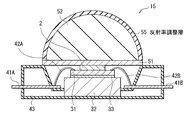
図1は、本発明の第1の実施の形態に係る半導体発光装置(LED装置1)の断面構成を表したものである。
ni≦np≦nc ……(1)
ni≧np≧nc ……(2)
(np×dp)=(2m+1)×λ/4 (m:0以上の整数) ……(3)
np=(ni×nc)1/2 ……(4)

図3は、第2の実施の形態に係る半導体発光装置(LED装置11)の断面構成を表すものである。
図6は、第3の実施の形態に係る半導体発光装置(LED装置13)の断面構成を表すものである。
Claims (16)
- 金属元素を含む半導体発光素子と、
硫黄(S)またはハロゲン元素を含むと共に前記半導体発光素子からの光を透過可能な材料からなるキャップ部と、
前記キャップ部と前記半導体発光素子との間に注入されており、硫黄(S)およびハロゲン元素を含まない材料からなると共に、前記キャップ部とともに前記半導体発光素子を外部から封止するための充填剤と、
前記キャップ部と前記充填剤との間に設けられ、前記半導体発光素子からの光を前記キャップ部へ透過させると共に前記半導体発光素子側と前記キャップ部側との間を遮蔽する遮蔽膜と
を備えた半導体発光装置。 - 前記半導体発光素子は、基板上に発光層を含む半導体積層構造を有し、
前記金属元素は、前記半導体積層構造に設けられた電極に含まれている
請求項1に記載の半導体発光装置。 - 前記基板は、前記発光層からの光を透過可能な透明基板である
請求項2に記載の半導体発光装置。 - 前記遮蔽膜は、前記電極に対応する位置に選択的に形成されている
請求項2に記載の半導体発光装置。 - 前記遮蔽膜は、前記キャップ部における前記半導体発光素子側の面上に形成されている
請求項1に記載の半導体発光装置。 - 前記遮蔽膜は、前記半導体発光素子と前記キャップ部との間に一様に形成されている
請求項1に記載の半導体発光装置。 - 前記半導体発光素子における前記遮蔽膜側とは反対側に、前記金属元素を含む部材が設けられている
請求項1に記載の半導体発光装置。 - 前記キャップ部の屈折率をnc、前記遮蔽膜の屈折率をnp、および前記遮蔽膜が前記半導体発光素子側で接する部材の屈折率をniとした場合に、前記遮蔽膜の屈折率は以下の(1)式または(2)式を満たす
請求項1ないし請求項7のいずれか1項に記載の半導体発光装置。
ni≦np≦nc ……(1)
ni≧np≧nc ……(2) - 前記半導体発光素子からの光における最大ピーク強度領域の波長をλ、および前記遮蔽膜の膜厚をdpとした場合に、前記遮蔽膜の屈折率および膜厚は以下の(3)式を満たす
請求項8に記載の半導体発光装置。
(np×dp)=(2m+1)×λ/4 (m:0以上の整数) ……(3) - 前記半導体発光素子のピーク発振波長(λ)は、630±50nmである
請求項9に記載の半導体発光装置。 - 前記半導体発光素子のピーク発振波長(λ)は、530±30nmである
請求項9に記載の半導体発光装置。 - 前記半導体発光素子のピーク発振波長(λ)は、460±60nmである
請求項9に記載の半導体発光装置。 - 前記遮蔽膜の屈折率は、以下の(4)式を満たす
請求項9ないし請求項12のいずれか1項に記載の半導体発光装置。
np=(ni×nc)1/2 ……(4) - 前記遮蔽膜は、酸化シリコン(SiO2)、窒化シリコン(Si3N4)、酸化アルミニウム(Al2O3)、窒化アルミニウム(AlN)、酸化マグネシウム(MgO)、酸化スズ(SnO)、酸化亜鉛(ZnO)、酸化インジウム(In2O3)、酸化ネオジム(Nd2O3)、酸化チタン(TiO2)および酸化ジリコニウム(ZrO2)からなる群のうちの少なくとも1種類を含んで構成されている
請求項1ないし請求項13のいずれか1項に記載の半導体発光装置。 - 前記キャップ部における前記半導体発光素子側とは反対側の面上に、このキャップ部と空気層との界面での反射率を調整するための反射率調整層を備えた
請求項1ないし請求項14のいずれか1項に記載の半導体発光装置。 - 光源装置に用いられる半導体発光装置組立体であって、
配線基板と、
前記配線基板と電気的に接続された複数の半導体発光装置と
を備え、
前記複数の半導体発光装置はそれぞれ、
金属元素を含む半導体発光素子と、
硫黄(S)またはハロゲン元素を含むと共に前記半導体発光素子からの光を透過可能な材料からなるキャップ部と、
前記キャップ部と前記半導体発光素子との間に注入されており、硫黄(S)およびハロゲン元素を含まない材料からなると共に、前記キャップ部とともに前記半導体発光素子を外部から封止するための充填剤と、
前記キャップ部と前記充填剤との間に設けられ、前記半導体発光素子からの光を前記キャップ部へ透過させると共に前記半導体発光素子側と前記キャップ部側との間を遮蔽する遮蔽膜と
を有する半導体発光装置組立体。
Priority Applications (4)
| Application Number | Priority Date | Filing Date | Title |
|---|---|---|---|
| JP2006014893A JP4952884B2 (ja) | 2006-01-24 | 2006-01-24 | 半導体発光装置および半導体発光装置組立体 |
| TW096101640A TW200742125A (en) | 2006-01-24 | 2007-01-16 | Semiconductor light emitting device, and assembly thereof |
| US11/656,358 US8035120B2 (en) | 2006-01-24 | 2007-01-22 | Semiconductor light emitting device and semiconductor light emitting device assembly |
| CNB2007100073430A CN100539221C (zh) | 2006-01-24 | 2007-01-23 | 半导体发光器件和半导体发光器件组装体 |
Applications Claiming Priority (1)
| Application Number | Priority Date | Filing Date | Title |
|---|---|---|---|
| JP2006014893A JP4952884B2 (ja) | 2006-01-24 | 2006-01-24 | 半導体発光装置および半導体発光装置組立体 |
Publications (3)
| Publication Number | Publication Date |
|---|---|
| JP2007200969A JP2007200969A (ja) | 2007-08-09 |
| JP2007200969A5 JP2007200969A5 (ja) | 2009-02-05 |
| JP4952884B2 true JP4952884B2 (ja) | 2012-06-13 |
Family
ID=38284662
Family Applications (1)
| Application Number | Title | Priority Date | Filing Date |
|---|---|---|---|
| JP2006014893A Expired - Fee Related JP4952884B2 (ja) | 2006-01-24 | 2006-01-24 | 半導体発光装置および半導体発光装置組立体 |
Country Status (4)
| Country | Link |
|---|---|
| US (1) | US8035120B2 (ja) |
| JP (1) | JP4952884B2 (ja) |
| CN (1) | CN100539221C (ja) |
| TW (1) | TW200742125A (ja) |
Families Citing this family (25)
| Publication number | Priority date | Publication date | Assignee | Title |
|---|---|---|---|---|
| TWI271883B (en) * | 2005-08-04 | 2007-01-21 | Jung-Chieh Su | Light-emitting devices with high extraction efficiency |
| TWI321857B (en) * | 2006-07-21 | 2010-03-11 | Epistar Corp | A light emitting device |
| US7625104B2 (en) * | 2007-12-13 | 2009-12-01 | Philips Lumileds Lighting Company, Llc | Light emitting diode for mounting to a heat sink |
| CN101546754A (zh) * | 2008-03-26 | 2009-09-30 | 富准精密工业(深圳)有限公司 | 发光二极管模组 |
| CN101561125A (zh) * | 2008-04-18 | 2009-10-21 | 富准精密工业(深圳)有限公司 | 发光二极管模组 |
| JP5199811B2 (ja) * | 2008-09-26 | 2013-05-15 | 浜松ホトニクス株式会社 | 光源装置 |
| KR101064026B1 (ko) * | 2009-02-17 | 2011-09-08 | 엘지이노텍 주식회사 | 발광 디바이스 패키지 및 그 제조방법 |
| KR100999756B1 (ko) * | 2009-03-13 | 2010-12-08 | 엘지이노텍 주식회사 | 발광소자 및 그 제조방법 |
| TWI450415B (zh) * | 2010-03-23 | 2014-08-21 | Lg Innotek Co Ltd | 發光裝置、發光裝置封裝件及照明系統 |
| JP2011204986A (ja) * | 2010-03-26 | 2011-10-13 | Showa Denko Kk | ランプおよびランプの製造方法 |
| WO2011145794A1 (ko) | 2010-05-18 | 2011-11-24 | 서울반도체 주식회사 | 파장변환층을 갖는 발광 다이오드 칩과 그 제조 방법, 및 그것을 포함하는 패키지 및 그 제조 방법 |
| CN103003966B (zh) * | 2010-05-18 | 2016-08-10 | 首尔半导体株式会社 | 具有波长变换层的发光二级管芯片及其制造方法,以及包括其的封装件及其制造方法 |
| CN102074641A (zh) * | 2010-07-23 | 2011-05-25 | 宁波市瑞康光电有限公司 | 一种led封装方法、led和led照明装置 |
| CN102468400B (zh) * | 2010-11-12 | 2015-05-06 | 良盟塑胶股份有限公司 | Led封装结构及其制作方法 |
| EP2466655A1 (en) * | 2010-12-14 | 2012-06-20 | Liang Meng Plastic Share Co. Ltd. | LED package structure and manufacturing method for the same |
| KR20120092000A (ko) | 2011-02-09 | 2012-08-20 | 서울반도체 주식회사 | 파장변환층을 갖는 발광 소자 |
| CN103187507A (zh) * | 2011-12-30 | 2013-07-03 | 展晶科技(深圳)有限公司 | 发光二极管封装结构 |
| CN103296182B (zh) * | 2012-03-01 | 2016-09-21 | 展晶科技(深圳)有限公司 | 发光二极管灯源装置 |
| US20140175473A1 (en) * | 2012-12-21 | 2014-06-26 | Cree, Inc. | Light emitting diodes including light emitting surface barrier layers, and methods of fabricating same |
| US9303857B2 (en) * | 2013-02-04 | 2016-04-05 | Cree, Inc. | LED lamp with omnidirectional light distribution |
| KR102038623B1 (ko) * | 2013-08-21 | 2019-10-30 | 삼성전자주식회사 | 광변조기 및 이를 포함한 3차원 영상 획득 장치 |
| KR102122359B1 (ko) * | 2013-12-10 | 2020-06-12 | 삼성전자주식회사 | 발광장치 제조방법 |
| US20220209166A1 (en) * | 2019-04-11 | 2022-06-30 | Sharp Kabushiki Kaisha | Light-emitting element and display device |
| KR20210132786A (ko) * | 2020-04-27 | 2021-11-05 | 삼성디스플레이 주식회사 | 화소 및 이를 구비한 표시 장치 |
| CN117038830A (zh) * | 2023-08-28 | 2023-11-10 | 广东光沐半导体科技有限公司 | 一种led防硫封装结构及封装工艺 |
Family Cites Families (16)
| Publication number | Priority date | Publication date | Assignee | Title |
|---|---|---|---|---|
| JPH01223780A (ja) * | 1988-03-02 | 1989-09-06 | Mitsubishi Cable Ind Ltd | 発光ダイオード素子 |
| JPH03155925A (ja) | 1989-11-15 | 1991-07-03 | Aikou:Kk | 樹脂成形品の製造方法およびそれに使用する成形用型 |
| JP2989787B2 (ja) | 1991-08-08 | 1999-12-13 | 三井化学株式会社 | 含硫ウレタン系樹脂及びレンズ |
| JP3155925B2 (ja) | 1995-05-12 | 2001-04-16 | 三井化学株式会社 | ポリスルフィド系樹脂組成物、該樹脂及びその樹脂よりなる光学材料 |
| US6650044B1 (en) * | 2000-10-13 | 2003-11-18 | Lumileds Lighting U.S., Llc | Stenciling phosphor layers on light emitting diodes |
| JP4101468B2 (ja) * | 2001-04-09 | 2008-06-18 | 豊田合成株式会社 | 発光装置の製造方法 |
| US6878973B2 (en) * | 2001-08-23 | 2005-04-12 | Lumileds Lighting U.S., Llc | Reduction of contamination of light emitting devices |
| US20040012027A1 (en) * | 2002-06-13 | 2004-01-22 | Cree Lighting Company | Saturated phosphor solid state emitter |
| US6717362B1 (en) * | 2002-11-14 | 2004-04-06 | Agilent Technologies, Inc. | Light emitting diode with gradient index layering |
| JP4572604B2 (ja) * | 2003-06-30 | 2010-11-04 | 日亜化学工業株式会社 | 半導体発光素子及びそれを用いた発光装置 |
| JP2005191220A (ja) * | 2003-12-25 | 2005-07-14 | Sanken Electric Co Ltd | 半導体発光素子およびその製造方法 |
| JP4330476B2 (ja) * | 2004-03-29 | 2009-09-16 | スタンレー電気株式会社 | 半導体発光素子 |
| US8134292B2 (en) * | 2004-10-29 | 2012-03-13 | Ledengin, Inc. | Light emitting device with a thermal insulating and refractive index matching material |
| US20060138443A1 (en) * | 2004-12-23 | 2006-06-29 | Iii-N Technology, Inc. | Encapsulation and packaging of ultraviolet and deep-ultraviolet light emitting diodes |
| JP2007109915A (ja) * | 2005-10-14 | 2007-04-26 | Stanley Electric Co Ltd | 発光ダイオード |
| US7473939B2 (en) * | 2006-01-06 | 2009-01-06 | Formosa Epitaxy Incorporation | Light-emitting diode structure with transparent window covering layer of multiple films |
-
2006
- 2006-01-24 JP JP2006014893A patent/JP4952884B2/ja not_active Expired - Fee Related
-
2007
- 2007-01-16 TW TW096101640A patent/TW200742125A/zh unknown
- 2007-01-22 US US11/656,358 patent/US8035120B2/en not_active Expired - Fee Related
- 2007-01-23 CN CNB2007100073430A patent/CN100539221C/zh not_active Expired - Fee Related
Also Published As
| Publication number | Publication date |
|---|---|
| US8035120B2 (en) | 2011-10-11 |
| TW200742125A (en) | 2007-11-01 |
| CN100539221C (zh) | 2009-09-09 |
| US20070170448A1 (en) | 2007-07-26 |
| JP2007200969A (ja) | 2007-08-09 |
| CN101009351A (zh) | 2007-08-01 |
Similar Documents
| Publication | Publication Date | Title |
|---|---|---|
| JP4952884B2 (ja) | 半導体発光装置および半導体発光装置組立体 | |
| JP4899825B2 (ja) | 半導体発光素子、発光装置 | |
| US10777715B2 (en) | Semiconductor light emitting device | |
| EP2312659B1 (en) | Light emitting apparatus | |
| CN106415836B (zh) | 半导体器件和照明设备 | |
| CN110676367B (zh) | 发光二极管 | |
| JP2006100787A (ja) | 発光装置および発光素子 | |
| JP2009088521A (ja) | 窒化ガリウム系発光ダイオード素子 | |
| KR20020003101A (ko) | 반도체 발광소자와 그 제조방법 및 반도체 발광장치 | |
| US20140167092A1 (en) | Optoelectronic assembly and method for producing an optoelectronic assembly | |
| JP3985332B2 (ja) | 半導体発光装置 | |
| US10326064B2 (en) | Light emitting device and method of manufacturing same | |
| JP2007194401A (ja) | 化合物半導体発光素子を用いたledパッケージ | |
| JP2014139997A (ja) | 発光素子および発光素子パッケージ | |
| JP2006066449A (ja) | 半導体発光素子 | |
| JP2005026395A (ja) | 半導体発光素子及び半導体発光装置 | |
| JP2020533778A (ja) | 発光素子パッケージ | |
| KR20120002130A (ko) | 플립칩형 발광 소자 및 그 제조 방법 | |
| JP2006073618A (ja) | 光学素子およびその製造方法 | |
| KR20130014692A (ko) | 곡선 기판을 갖는 led 칩과 이를 이용한 led 패키지 | |
| JP2007221175A (ja) | 半導体発光素子及び半導体発光装置 | |
| JP2018026597A (ja) | 発光素子および発光素子パッケージ | |
| JP6892909B2 (ja) | 発光素子および発光素子パッケージ | |
| KR102133904B1 (ko) | 발광 다이오드 유전체 거울 | |
| JPH11112021A (ja) | 半導体発光装置 |
Legal Events
| Date | Code | Title | Description |
|---|---|---|---|
| A521 | Written amendment |
Free format text: JAPANESE INTERMEDIATE CODE: A523 Effective date: 20081211 |
|
| A621 | Written request for application examination |
Free format text: JAPANESE INTERMEDIATE CODE: A621 Effective date: 20081211 |
|
| A131 | Notification of reasons for refusal |
Free format text: JAPANESE INTERMEDIATE CODE: A131 Effective date: 20110419 |
|
| A977 | Report on retrieval |
Free format text: JAPANESE INTERMEDIATE CODE: A971007 Effective date: 20110420 |
|
| A521 | Written amendment |
Free format text: JAPANESE INTERMEDIATE CODE: A523 Effective date: 20110608 |
|
| TRDD | Decision of grant or rejection written | ||
| A01 | Written decision to grant a patent or to grant a registration (utility model) |
Free format text: JAPANESE INTERMEDIATE CODE: A01 Effective date: 20120215 |
|
| A01 | Written decision to grant a patent or to grant a registration (utility model) |
Free format text: JAPANESE INTERMEDIATE CODE: A01 |
|
| A61 | First payment of annual fees (during grant procedure) |
Free format text: JAPANESE INTERMEDIATE CODE: A61 Effective date: 20120228 |
|
| FPAY | Renewal fee payment (event date is renewal date of database) |
Free format text: PAYMENT UNTIL: 20150323 Year of fee payment: 3 |
|
| LAPS | Cancellation because of no payment of annual fees |