JP4952884B2 - Semiconductor light emitting device and semiconductor light emitting device assembly - Google Patents
Semiconductor light emitting device and semiconductor light emitting device assembly Download PDFInfo
- Publication number
- JP4952884B2 JP4952884B2 JP2006014893A JP2006014893A JP4952884B2 JP 4952884 B2 JP4952884 B2 JP 4952884B2 JP 2006014893 A JP2006014893 A JP 2006014893A JP 2006014893 A JP2006014893 A JP 2006014893A JP 4952884 B2 JP4952884 B2 JP 4952884B2
- Authority
- JP
- Japan
- Prior art keywords
- semiconductor light
- light emitting
- emitting device
- shielding film
- cap
- Prior art date
- Legal status (The legal status is an assumption and is not a legal conclusion. Google has not performed a legal analysis and makes no representation as to the accuracy of the status listed.)
- Expired - Fee Related
Links
Images


Classifications
-
- H—ELECTRICITY
- H01—ELECTRIC ELEMENTS
- H01L—SEMICONDUCTOR DEVICES NOT COVERED BY CLASS H10
- H01L33/00—Semiconductor devices with at least one potential-jump barrier or surface barrier specially adapted for light emission; Processes or apparatus specially adapted for the manufacture or treatment thereof or of parts thereof; Details thereof
- H01L33/48—Semiconductor devices with at least one potential-jump barrier or surface barrier specially adapted for light emission; Processes or apparatus specially adapted for the manufacture or treatment thereof or of parts thereof; Details thereof characterised by the semiconductor body packages
- H01L33/58—Optical field-shaping elements
-
- H—ELECTRICITY
- H01—ELECTRIC ELEMENTS
- H01L—SEMICONDUCTOR DEVICES NOT COVERED BY CLASS H10
- H01L2224/00—Indexing scheme for arrangements for connecting or disconnecting semiconductor or solid-state bodies and methods related thereto as covered by H01L24/00
- H01L2224/01—Means for bonding being attached to, or being formed on, the surface to be connected, e.g. chip-to-package, die-attach, "first-level" interconnects; Manufacturing methods related thereto
- H01L2224/42—Wire connectors; Manufacturing methods related thereto
- H01L2224/47—Structure, shape, material or disposition of the wire connectors after the connecting process
- H01L2224/48—Structure, shape, material or disposition of the wire connectors after the connecting process of an individual wire connector
- H01L2224/4805—Shape
- H01L2224/4809—Loop shape
- H01L2224/48091—Arched
-
- H—ELECTRICITY
- H01—ELECTRIC ELEMENTS
- H01L—SEMICONDUCTOR DEVICES NOT COVERED BY CLASS H10
- H01L2224/00—Indexing scheme for arrangements for connecting or disconnecting semiconductor or solid-state bodies and methods related thereto as covered by H01L24/00
- H01L2224/73—Means for bonding being of different types provided for in two or more of groups H01L2224/10, H01L2224/18, H01L2224/26, H01L2224/34, H01L2224/42, H01L2224/50, H01L2224/63, H01L2224/71
- H01L2224/732—Location after the connecting process
- H01L2224/73251—Location after the connecting process on different surfaces
- H01L2224/73265—Layer and wire connectors
-
- H—ELECTRICITY
- H01—ELECTRIC ELEMENTS
- H01L—SEMICONDUCTOR DEVICES NOT COVERED BY CLASS H10
- H01L2924/00—Indexing scheme for arrangements or methods for connecting or disconnecting semiconductor or solid-state bodies as covered by H01L24/00
- H01L2924/30—Technical effects
- H01L2924/301—Electrical effects
- H01L2924/3025—Electromagnetic shielding
-
- H—ELECTRICITY
- H01—ELECTRIC ELEMENTS
- H01L—SEMICONDUCTOR DEVICES NOT COVERED BY CLASS H10
- H01L33/00—Semiconductor devices with at least one potential-jump barrier or surface barrier specially adapted for light emission; Processes or apparatus specially adapted for the manufacture or treatment thereof or of parts thereof; Details thereof
- H01L33/44—Semiconductor devices with at least one potential-jump barrier or surface barrier specially adapted for light emission; Processes or apparatus specially adapted for the manufacture or treatment thereof or of parts thereof; Details thereof characterised by the coatings, e.g. passivation layer or anti-reflective coating
-
- H—ELECTRICITY
- H01—ELECTRIC ELEMENTS
- H01L—SEMICONDUCTOR DEVICES NOT COVERED BY CLASS H10
- H01L33/00—Semiconductor devices with at least one potential-jump barrier or surface barrier specially adapted for light emission; Processes or apparatus specially adapted for the manufacture or treatment thereof or of parts thereof; Details thereof
- H01L33/48—Semiconductor devices with at least one potential-jump barrier or surface barrier specially adapted for light emission; Processes or apparatus specially adapted for the manufacture or treatment thereof or of parts thereof; Details thereof characterised by the semiconductor body packages
- H01L33/52—Encapsulations
- H01L33/54—Encapsulations having a particular shape
Description
本発明は、樹脂材料を成分とするキャップ部を備えた半導体発光装置、およびその半導体発光装置を備えた光源装置用の半導体発光装置組立体に関する。 The present invention relates to a semiconductor light-emitting device including a cap portion including a resin material as a component, and a semiconductor light-emitting device assembly for a light source device including the semiconductor light-emitting device.
近年、GaN系半導体やInGaN系半導体を用いた発光ダイオード(LED;Light Emitting Diode)では、光の取り出し効率を向上させるため、いわゆる裏面発光型(フリップチップ型)LEDが主流となっている。このフリップチップ型LEDとは、透明基板と反射電極との間に活性層を含む半導体積層構造を配置したものであり、これにより活性層から発せられた光を裏面側(透明基板側)から射出させるようになっている。 In recent years, light-emitting diodes (LEDs) using GaN-based semiconductors or InGaN-based semiconductors have become the mainstream in order to improve the light extraction efficiency. This flip chip type LED is a semiconductor laminated structure including an active layer between a transparent substrate and a reflective electrode, and thereby light emitted from the active layer is emitted from the back side (transparent substrate side). It is supposed to let you.
図11は、フリップチップ型LEDを用いた従来の半導体発光装置(LED装置101)の断面構成例を表したものである。このLED装置101では、射出光L101を発するLEDチップ102がサブマウント基板131上に配置され、ボンディングワイヤ142A,142Bによって、LEDチップ102内の電極(図示せず)とリードフレーム電極141A,141Bとが電気的に接続されている。また、サブマウント基板131は、熱伝導性接着剤133によって、放熱構造体であるスラグ132と接着されている。スラグ132およびリードフレーム電極141A,141Bの一部は、ケース143によって覆われている。また、LEDチップ102の周囲も充填剤154およびキャップ152によって覆われ、外部から封止されるようになっている。
FIG. 11 illustrates a cross-sectional configuration example of a conventional semiconductor light emitting device (LED device 101) using a flip chip type LED. In this
充填剤154としては、例えばシリコーンゲルのような柔軟性の高い材料や、流動性の高い材料などが用いられている。一方、キャップ152としては、エポキシ系樹脂等が用いられているほか、例えば特許文献1〜4に示された樹脂材料が提案されている。なお、例えばエポキシ系樹脂のような硬い材料を用いた場合には、充填剤がキャップとしても機能するようになっている。
As the
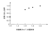
ところで、LED装置の光取り出し効率を高めるには、充填剤やキャップの屈折率を、できるだけLEDチップ部分(フリップチップ型のLEDの場合、透明基板となる)の屈折率と近づけるのが望ましい。これらの界面でのフレネル反射が抑えられ、全反射を生じさせる臨界角も大きくなるからである。 By the way, in order to increase the light extraction efficiency of the LED device, it is desirable to make the refractive index of the filler or cap as close as possible to the refractive index of the LED chip portion (which is a transparent substrate in the case of flip-chip type LEDs). This is because Fresnel reflection at these interfaces is suppressed, and the critical angle causing total reflection increases.
通常、透明基板としてはサファイア基板が用いられることから、透明基板の屈折率は1.70〜1.80程度である。一方、充填剤やキャップの屈折率は、一般にサファイア基板と比べて相当小さく、例えばエポキシ系樹脂の屈折率は1.40〜1.55程度である。したがって、例えば図12に示した特性図から分かるように、充填剤やキャップの屈折率が高い場合(1.80程度の場合)と比べ、光取り出し効率が約15〜20%も低下してしまうことになる。 Usually, since a sapphire substrate is used as the transparent substrate, the refractive index of the transparent substrate is about 1.70 to 1.80. On the other hand, the refractive index of the filler or cap is generally considerably smaller than that of the sapphire substrate. For example, the refractive index of the epoxy resin is about 1.40 to 1.55. Therefore, for example, as can be seen from the characteristic diagram shown in FIG. 12, the light extraction efficiency is reduced by about 15 to 20% as compared with the case where the refractive index of the filler or cap is high (about 1.80). It will be.
ここで、上記特許文献1〜4に示された樹脂材料では、その屈折率が1.70〜1.74程度と高く、フリップチップ型LEDにおけるサファイア基板のものと近いことから、従来よりも光取り出し効率を向上させることができると考えられる。
Here, in the resin materials shown in
ところが、これらの高屈折率樹脂材料は、いずれも銀(Ag)等の金属元素との反応性が高い硫黄(S)やハロゲン元素を含んでいるため、例えば図13に示した特性図(順方向電流If=350mA,環境温度=85℃の条件下におけるLED装置から射出する光束量の時間変化)のように、LED装置の発光特性を経時的に劣化させてしまうことが分かった。 However, since these high refractive index resin materials all contain sulfur (S) and halogen elements that are highly reactive with metal elements such as silver (Ag), the characteristic diagram shown in FIG. It has been found that the light emission characteristics of the LED device are deteriorated over time, as in the case of the direction current If = 350 mA and the environmental temperature = 85 ° C.
具体的には、LEDチップ内の電極や、サブマウント基板とスラグとを接着する熱伝導性接着剤などには上記金属元素が用いられているため、イオンマイグレーションによって容易に硫黄やハロゲン元素と反応してしまう。よって、例えばAgの場合には反応すると褐色の硫化銀(AgS)やハロゲン化銀となることから、LED装置の発光特性が経時的に劣化してしまうことになる。 Specifically, the metal element is used for the electrode in the LED chip and the heat conductive adhesive that bonds the submount substrate and the slag, so it easily reacts with sulfur and halogen elements by ion migration. Resulting in. Therefore, for example, in the case of Ag, the reaction results in brown silver sulfide (AgS) or silver halide, so that the light emission characteristics of the LED device deteriorate over time.
このように、充填剤やキャップとして硫黄やハロゲン元素を含む樹脂材料を用いざるを得ない従来の技術では、発光特性の経時劣化を防止しつつ光取り出し効率を向上させるのが困難であった。 As described above, in the conventional technique in which a resin material containing sulfur or a halogen element has to be used as a filler or a cap, it is difficult to improve light extraction efficiency while preventing deterioration of light emission characteristics with time.
本発明はかかる問題点に鑑みてなされたもので、その目的は、発光特性の経時劣化を防止しつつ光取り出し効率を向上させることが可能な半導体発光装置、およびそのような半導体発光装置を備えた半導体発光装置組立体を提供することにある。 The present invention has been made in view of such problems, and an object thereof is to provide a semiconductor light emitting device capable of improving light extraction efficiency while preventing deterioration of light emission characteristics over time, and such a semiconductor light emitting device. Another object of the present invention is to provide a semiconductor light emitting device assembly.
本発明の半導体発光装置は、金属元素を含む半導体発光素子と、硫黄(S)またはハロゲン元素を含むと共に上記半導体発光素子からの光を透過可能な材料からなるキャップ部と、このキャップ部と半導体発光素子との間に注入されており、硫黄(S)およびハロゲン元素を含まない材料からなると共に、キャップ部とともに半導体発光素子を外部から封止するための充填剤と、キャップ部と充填剤との間に設けられ、半導体発光素子からの光をキャップ部へ透過させると共に半導体発光素子側とキャップ部側との間を遮蔽する遮蔽膜とを備えたものである。 The semiconductor light-emitting device of the present invention includes a semiconductor light-emitting element containing a metal element, a cap part that contains sulfur (S) or a halogen element and is capable of transmitting light from the semiconductor light-emitting element, and the cap part and the semiconductor A filler that is injected between the light emitting element and is made of a material that does not contain sulfur (S) and halogen elements; and a cap for sealing the semiconductor light emitting element from the outside together with the cap; provided between, in which a shielding film for shielding between the semiconductor light-emitting element side and the cap portion side together to transmit light from the semi-conductor light emitting element to the cap portion.
本発明の半導体発光装置組立体は、バックライトなどの光源装置に用いられるものであって、配線基板上に上記半導体発光装置を複数個搭載したものである。 The semiconductor light emitting device assembly of the present invention is used for a light source device such as a backlight, and a plurality of the semiconductor light emitting devices are mounted on a wiring board.
本発明の半導体発光装置および半導体発光装置組立体では、遮蔽膜によって半導体発光素子側とキャップ部側との間が遮蔽されるため、半導体発光素子内の金属元素とキャップ部内の硫黄(S)またはハロゲン元素との反応が防止される。 In the semiconductor light emitting device and the semiconductor light emitting device assembly of the present invention, the shielding film shields between the semiconductor light emitting element side and the cap part side, so that the metal element in the semiconductor light emitting element and sulfur (S) in the cap part or Reaction with halogen elements is prevented.
本発明の半導体発光装置では、上記キャップ部の屈折率をnc、上記遮蔽膜の屈折率をnp、および上記遮蔽膜が半導体発光素子側で接する部材の屈折率をniとした場合に、遮蔽膜の屈折率が以下の(1)式または(2)式を満たすようにするのが好ましい。このように構成した場合、半導体発光素子とキャップ部との間の屈折率差が遮蔽膜によって緩和され、半導体発光素子から外部へと向かう際のフレネル反射が低減する。
ni≦np≦nc ……(1)
ni≧np≧nc ……(2)
In the semiconductor light emitting device of the present invention, when the refractive index of the cap portion is nc, the refractive index of the shielding film is np, and the refractive index of the member that the shielding film contacts on the semiconductor light emitting element side is ni, the shielding film It is preferable to satisfy the following formula (1) or (2). When comprised in this way, the refractive index difference between a semiconductor light-emitting device and a cap part is relieve | moderated by a shielding film, and the Fresnel reflection at the time of going to the exterior from a semiconductor light-emitting device reduces.
ni ≦ np ≦ nc (1)
ni ≧ np ≧ nc (2)
本発明の半導体発光装置または半導体発光装置組立体によれば、半導体発光素子とキャップ部との間に遮蔽膜を設けるようにしたので、金属元素と硫黄(S)またはハロゲン元素との反応を防止することができ、発光特性の経時劣化を防止しつつ光取り出し効率を向上させることが可能となる。 According to the semiconductor light emitting device or the semiconductor light emitting device assembly of the present invention, since the shielding film is provided between the semiconductor light emitting element and the cap portion, the reaction between the metal element and sulfur (S) or the halogen element is prevented. Therefore, it is possible to improve the light extraction efficiency while preventing the light emission characteristics from being deteriorated over time.
特に、遮蔽膜の屈折率が上記(1)式または(2)式を満たすようにした場合には、半導体発光素子から外部へと向かう際のフレネル反射を低減することができ、光取り出し効率をより向上させることが可能となる。 In particular, when the refractive index of the shielding film satisfies the above formula (1) or (2), Fresnel reflection when going from the semiconductor light emitting element to the outside can be reduced, and the light extraction efficiency can be reduced. This can be further improved.
以下、本発明の実施の形態について、図面を参照して詳細に説明する。 Hereinafter, embodiments of the present invention will be described in detail with reference to the drawings.
[第1の実施の形態]
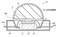
図1は、本発明の第1の実施の形態に係る半導体発光装置(LED装置1)の断面構成を表したものである。
[First Embodiment]
FIG. 1 shows a cross-sectional configuration of a semiconductor light emitting device (LED device 1) according to a first embodiment of the present invention.
このLED装置1では、上方に光L1を発するLEDチップ2がサブマウント基板31上に設置されている。サブマウント基板31は、ボンディングワイヤ42A,42Bによって、リードフレーム電極41A,41Bと電気的に接続されている。サブマウント基板31の裏面は、熱伝導性接着剤33によって、放熱構造体であるスラグ32と接着されている。スラグ32およびリードフレーム電極41A,41Bの一部は、ケース43によって覆われている。また、LEDチップ2およびケース43上には、その上方を凸面とした半球状のキャップ52が配置されている。このキャップ52とLEDチップ2との間、すなわちキャップ52の底面には、遮蔽膜51が一様に形成されている。
In this
図2は、このLED装置1のうちの一部分(LEDチップ2付近)の断面構成を詳細に表したものである。 FIG. 2 shows in detail a cross-sectional configuration of a part of the LED device 1 (in the vicinity of the LED chip 2).
このフリップチップ型のLEDチップ2は、基板として透明基板21を有している。この透明基板21の表面にはキャップ52側の遮蔽膜51が密着している。透明基板21の裏面には、n型クラッド層22が一様に形成されている。n型クラッド層22の一部にはn型電極26が形成され、他の一部には活性層23、p型クラッド層24およびp型電極25が順次形成され、リッジ状の積層構造をなしている。また、n型電極26およびp型電極25はそれぞれ、はんだ等からなるバンプ31Bによってサブマウント基板31上の電極31Aと電気的に接続されている。すなわち、n型電極26はバンプ31B、電極31Aおよびボンディングワイヤ42Aを介してリードフレーム電極41Aと電気的に接続され、p型電極25はバンプ31B、電極31Aおよびボンディングワイヤ42Bを介してリードフレーム電極41Bと電気的に接続されている。このような構成によりLEDチップ2は、活性層23から発せられた光を最終的にキャップ部52を通じて上方から射出(射出光L1)するようになっている。
The flip chip
透明基板21は活性層23からの光に対して透明な基板であり、例えばサファイア基板などにより構成される。活性層23は不純物が添加されていない半導体材料により構成され、供給された電流により光を発する発光領域として機能する。また、n型クラッド層22およびp型クラッド層24はそれぞれ、n型またはp型の半導体多層膜により構成されており、活性層23に対して電子または正孔を供給する。これらn型クラッド層22、活性層23およびp型クラッド層24はそれぞれ、例えば、430〜560nm程度の波長領域を対象とする緑色・青色発光材料であるGaN系またはInGaN系の半導体などにより構成される。
The transparent substrate 21 is a substrate that is transparent to the light from the active layer 23, and is composed of, for example, a sapphire substrate. The active layer 23 is made of a semiconductor material to which no impurity is added, and functions as a light emitting region that emits light by a supplied current. The n-
n型電極26およびp型電極25はそれぞれ活性層23に対して電流を供給するためのものであり、リードフレーム電極41A,41Bを介して直流電源(図示せず)が接続される。また、p型電極25は、活性層23からの光のうちのp型電極25側の光を反射し、透明基板21側へ導く反射電極としても機能する。n型電極26は例えばチタン(Ti)などの仕事関数の小さな金属元素により構成され、p型電極25は反射率が高い金属元素、例えば、銀(Ag)、金(Au)、アルミニウム(Al)などにより構成される。なお、このp型電極25が、本発明における「金属元素からなる電極」の一具体例に対応する。
The n-
図1の説明に戻ると、熱伝導性接着剤33は上記金属元素を含む接着剤からなり、例えばAgを含む熱伝導性エポキシ系接着剤などにより構成される。この熱伝導性接着剤33が、本発明における「金属元素を含む部材」の一具体例に対応する。
Returning to the description of FIG. 1, the heat
キャップ52は、LEDチップ2を外部から封止すると共に、LEDチップ2からの光を透過し、外部へ射出するためのものであり、硫黄(S)やハロゲン元素を含む高屈折率性の樹脂材料を成分としている。具体的には例えば、含硫ポリウレタン系樹脂(屈折率:1.70)、含硫アクリル系樹脂(屈折率:1.70)および含硫エポキシ系樹脂(屈折率:1.70)などが挙げられる。
The
遮蔽膜51は、LEDチップ2とキャップ52との間に配置され、LEDチップ2からの光L1を透過する一方、これらの間での元素の移動を遮蔽する役割を果たしている。具体的には、LEDチップ2内のp型電極25や熱伝導性接着剤33に含まれる金属元素がイオンマイグレーション等によりキャップ52へ侵入するのを遮蔽し、これら金属元素とキャップ52内の硫黄やハロゲン元素との反応を防止するようになっている。
The shielding
遮蔽膜51の屈折率は、キャップ52における樹脂材料の屈折率をnc、遮蔽膜51の屈折率をnp、および遮蔽膜51がLEDチップ2側で接する部材の屈折率をniとすると、以下の(1)式または(2)式を満たすのが望ましい。遮蔽膜51をそのような条件を満たす材料により構成した場合、LEDチップ2とキャップ52との間の屈折率差が遮蔽膜51によって緩和され、LEDチップ2から外部へと向かう際の各界面(LEDチップ2内の透明基板21と遮蔽膜51との界面、および遮蔽膜51とキャップ52との界面)でのフレネル反射が低減するからである。なお、本実施の形態のLED装置1では、遮蔽膜51がLEDチップ2側で接する部材は、このLEDチップ2がフリップチップ型であるため、透明基板21となる。
ni≦np≦nc ……(1)
ni≧np≧nc ……(2)
The refractive index of the shielding
ni ≦ np ≦ nc (1)
ni ≧ np ≧ nc (2)
また、遮蔽膜51の屈折率および膜厚は、LEDチップ2らの光L1における最大ピーク強度領域の波長をλ、および遮蔽膜51の膜厚をdpとすると、以下の(3)式を満たすのがより望ましい。遮蔽膜51をそのような条件を満たす材料により構成した場合、LEDチップ2内の透明基板21と遮蔽膜51との界面および遮蔽膜51とキャップ52との界面において、光束の干渉によってフレネル反射がより低減するからである。
(np×dp)=(2m+1)×λ/4 (m:0以上の整数) ……(3)
The refractive index and film thickness of the shielding
(Np × dp) = (2m + 1) × λ / 4 (m: integer greater than or equal to 0) (3)
なお、上記(3)式において、LEDチップ2のピーク発振波長(光L1における最大ピーク強度領域の波長λ)は、例えば、前述の半導体積層構造をInGaN等の緑色発光材料により構成した場合には530±20nm程度、InGaN等の青色発光材料により構成した場合には460±20nm程度である。 In the above equation (3), the peak oscillation wavelength of the LED chip 2 (the wavelength λ of the maximum peak intensity region in the light L1) is, for example, when the above-described semiconductor stacked structure is formed of a green light emitting material such as InGaN. In the case of a blue light emitting material such as InGaN, about 530 ± 20 nm, it is about 460 ± 20 nm.
また、遮蔽膜51の屈折率は、以下の(4)式を満たすのがさらに望ましい。遮蔽膜51をそのような条件を満たす材料により構成した場合、上記(3)式の場合と同様にしてフレネル反射が低減すると共に、(3)式におけるピーク発振波長λに対応する光L1のフレネル反射が0となる。
np=(ni×nc)1/2 ……(4)
Further, it is more desirable that the refractive index of the shielding
np = (ni × nc) 1/2 (4)
遮蔽膜51は、具体的には例えば表1に示した材料により構成される。すなわち、例えば酸化シリコン(SiO2)、窒化シリコン(Si3N4)、酸化アルミニウム(Al2O3)、窒化アルミニウム(AlN)、酸化マグネシウム(MgO)、酸化スズ(SnO)、酸化亜鉛(ZnO)、酸化インジウム(In2O3)、酸化ネオジム(Nd2O3)、酸化チタン(TiO2)または酸化ジリコニウム(ZrO2)などにより構成される。
Specifically, the shielding

また、遮蔽膜51を上記した材料の組み合わせ、すなわちこれらの材料からなる群のうちの少なくとも1種類を含むように構成してもよい。このような混合材料により構成した場合、各材料の組成比を変えることにより、遮蔽膜51の屈折率を自在に調整することができる。
Further, the shielding
なお表1には、上記した遮蔽膜51の構成材料と共に、透明基板21の構成材料例であるサファイア(屈折率:1.76)や、LEDチップ2内の半導体積層構造の構成材料例である緑色・青色発光材料のGaN(屈折率:2.40)や、後述する第2の実施の形態におけるLEDチップ6内の半導体積層構造の構成材料例である赤色発光材料のGaAs,AlGaAs(屈折率:3.30〜3.90)も載せている。
Table 1 shows examples of constituent materials of the sapphire (refractive index: 1.76) which is an example of the constituent material of the transparent substrate 21 and the semiconductor laminated structure in the
このLED装置1は、例えば以下のようにして製造することができる。
The
最初に、LEDチップ2を形成する。具体的にはまず、前述した材料よりなる透明基板21上に、前述した材料よりなるn型クラッド層22、活性層23およびp型クラッド層24を、例えば有機金属化学気相成長(MOCVD;Metal Organic Chemical Vapor Deposition)法や分子線エピタキシー(MBE;Molecular Beam Epitaxy)法により順次エピタキシャル成長させ、半導体積層構造を形成する。続いて、n型クラッド層22上にn型電極26を形成する位置を確保するため、n型クラッド層22、活性層23およびp型クラッド層24の一部を、所定の形状に加工する。この所定の形状への加工は、例えばリアクティブイオン加工(RIE;Reactive Ion Etching)や収束イオンビーム加工(FIB;Focused Ion Beam etching)などにより行う。続いて、n型クラッド層22上の一部にn型電極26を、そしてp型クラッド層24上にp型電極25を、それぞれ例えば蒸着法により形成する。これにより、図2に示したLEDチップ2が形成される。
First, the
次に、形成したLEDチップ2を、はんだ等からなるバンプ31Bにより、サブマウント基板31上に設置する。この際、図2に示したように、LEDチップ2上のn型電極26およびp型電極25とサブマウント基板31上の電極31Aとがバンプ31Bを介して電気的に接続するよう、位置合わせを行う。続いて、前述した材料よりなる熱伝導性接着剤33により、サブマウント基板31をスラグ32上に接着させる。
Next, the formed
次に、スラグ32およびリードフレーム電極41A,41Bの一部を、ケース43に装着する。そして、LEDチップ2内のn型電極26およびp型電極25とリードフレーム電極41A,41Bとの間を、ボンディングワイヤ42A,42Bによってそれぞれ接続し、これらの間を電気的に接続させる。
Next, the
一方、前述した樹脂材料を用いて、以下のようにしてキャップ52を形成する。すなわち、例えば熱硬化型樹脂や紫外線硬化型樹脂を金型成形することにより、例えば図1に示したような半球状のキャップ52を形成する。
On the other hand, the
続いて、このキャップ52における平面側に、前述した材料よりなる遮蔽膜51を、例えば酸素(O2)や窒素(N2)導入反応性のDCスパッタリング法またはRFスパッタリング法などにより、例えば220〜230nm程度の厚さで一様に形成する。
Subsequently, the flat side of the
最後に、このようにして形成されたLEDチップ2、サブマウント基板31、スラグ32、リードフレーム電極41A,42Bおよびケース43の構造体と、キャップ52および遮蔽膜51の構造体とを向かい合わせ、結合させる。具体的には、LEDチップ2と遮蔽膜51とが密着するようにキャップ52のエッジ付近とケース43とを樹脂で接着させ、上記2つの構造体同士を結合させる。このようにして、図1および図2に示したLED装置1が製造される。
Finally, in this way the
このLED装置1では、直流電源(図示せず)からリードフレーム電極41A,41Bおよびボンディングワイヤ42A,42Bを通じてn型電極26とp型電極25との間に所定の電圧が印加されると、n型クラッド層22またはp型クラッド層24を介して、活性層23へ電流が注入される。活性層23では、注入された電流により電子−正孔再結合が起こり、発光する。この光のうち、透明基板21側への光は、そのまま透明基板21、遮蔽膜51およびキャップ52を介して射出される。一方、p型電極25側への光は、このp型電極25により反射され、透明基板21側へ導かれる。このようにして、活性層23から発せられた光が最終的に射出光L1として、透明基板21側、すなわちLED装置1のキャップ52側へ射出される。
In this
ここで、このLED装置1では、LEDチップ2とキャップ52との間に遮蔽膜51が設けられているため、イオンマイグレーション等によるLEDチップ2とキャップ52との間での元素の移動が抑制され、LEDチップ2内の金属元素、具体的にはp型電極25および熱伝導性接着剤33に含まれる金属元素と、キャップ52内の硫黄またはハロゲン元素との反応が回避される。
Here, in this
また、この遮蔽膜51およびキャップ52は、LEDチップ2からの光L1を透過可能な材料により構成されているので、これらの部位において、射出光L1の光取り出し効率が低下することはない。
Further, since the shielding
以上のように、本実施の形態では、LEDチップ2とキャップ52との間に遮蔽膜51を設けるようにしたので、LEDチップ2内のp型電極25に含まれる金属元素とキャップ52に含まれる硫黄(S)またはハロゲン元素との反応を回避することができ、LED装置1の発光特性の経時劣化を防止しつつ、光取り出し効率を向上させることが可能となる。
As described above, in this embodiment, since the shielding
また、遮蔽膜51のLEDチップ2側には、LEDチップ2内の他に熱伝導性接着剤33内にも金属元素が含まれているので、p型電極25に含まれる金属元素に加え、この熱伝導性接着剤33に含まれる金属元素と上記硫黄またはハロゲン元素との反応も回避することができる。
Moreover, since the metal element is contained in the heat conductive adhesive 33 in addition to the
また、LEDチップ2とキャップ52との間に遮蔽膜51を一様に形成するようにしたので、後述するように遮蔽膜を選択的に形成した場合と比べてより完全に遮蔽することができ、上記した反応をより効果的に防止することが可能となる。
Further, since the shielding
また、遮蔽膜51の屈折率が前述の(1)式または(2)式を満たすようにした場合には、LEDチップ2から外部へと向かう際の各界面でのフレネル反射を抑えることができる。よって、光L1の反射率を低減させ、光取り出し効率をより向上させることが可能となる。
In addition, when the refractive index of the shielding
また、上記(1)式または(2)式に加え、遮蔽膜51の屈折率および膜厚が前述の(3)式も満たすようにした場合には、光束の干渉によって光L1の反射率を低減させ、光取り出し効率をさらに向上させることが可能となる。
In addition to the above formula (1) or (2), when the refractive index and film thickness of the shielding
また、上記(1)式〜(3)式に加え、遮蔽膜51の屈折率が前述の(4)式も満たすようにした場合には、ピーク発振波長λに対応する光L1の反射率をほぼ0とすることができる。よって、光取り出し効率を最大限に向上させることが可能となる。
In addition to the above formulas (1) to (3), when the refractive index of the shielding
また、遮蔽膜51を構成可能な材料を組み合わせ、これらの材料からなる群のうちの少なくとも1種類を含んで構成するようにした場合には、各材料の組成比を変えることにより、遮蔽膜51の屈折率を自在に調整することができる。よって、各材料の組成比を調整することにより、遮蔽膜51の屈折率が上記(1)〜(4)式を満たすように設定することが可能となる。
Further, in the case where materials capable of forming the shielding
さらに、キャップ52の裏面に遮蔽膜51を一様形成した後にこれをLEDチップ2等と結合させてLED装置1を製造するようにしたので、遮蔽膜51を容易に形成することができ、従来のLED装置と比べて特に複雑化することなく製造することができる。
Furthermore, since the
なお、本実施の形態における具体的な実施例(実施例1)としては、透明基板21としてサファイア基板(屈折率ni=1.76)を、キャップ52の構成樹脂として含硫ポリウレタン系樹脂(屈折率nc=1.70)を、遮蔽膜51として厚さが230nmのAl2O3(屈折率np=1.76)を用い、半導体積層構造として430〜560nm程度の波長領域を対象とする緑色・青色発光材料であるGaN系またはInGaN系の半導体を用いるものが挙げられる。なお、Al2O3からなる遮蔽膜51は、Al2ターゲットを用いたO2導入反応性DCスパッタリング法により形成する。この実施例1では、最大ピーク強度領域の波長λ=540nmとした場合、前述の(2)式および(3)式を満たしている((3)式においては、m=1)。
As a concrete example (Example 1) in the present embodiment, a sapphire substrate (refractive index ni = 1.76) is used as the transparent substrate 21, and a sulfur-containing polyurethane resin (refracted) is used as the constituent resin of the
また、本実施の形態における他の実施例(実施例2)としては、遮蔽膜51として厚さが230nmのSiOxNy(屈折率np=1.73)を用いるものが挙げられる。なお、このSiOxNyからなる遮蔽膜51は、SiO2ターゲットを用いたN2導入反応性RFスパッタリング法により形成する。この実施例2では、最大ピーク強度領域の波長λ=530nmとした場合、前述の(2)式〜(4)式を満たす((3)式においては、m=1)ため、上記実施例1と比べて光取り出し効率がより向上することになる。
Further, as another example (Example 2) in the present embodiment, a film using SiOxNy (refractive index np = 1.73) having a thickness of 230 nm may be used as the shielding
以下、本発明の他の実施の形態に係る半導体発光装置について説明する。なお、第1の実施の形態における構成要素と同一のものには同一の符号を付し、適宜説明を省略する。 Hereinafter, a semiconductor light emitting device according to another embodiment of the present invention will be described. In addition, the same code | symbol is attached | subjected to the same thing as the component in 1st Embodiment, and description is abbreviate | omitted suitably.
[第2の実施の形態]
図3は、第2の実施の形態に係る半導体発光装置(LED装置11)の断面構成を表すものである。
[Second Embodiment]
FIG. 3 illustrates a cross-sectional configuration of the semiconductor light emitting device (LED device 11) according to the second embodiment.
このLED装置11では、第1の実施の形態(LED装置1)で説明したフリップチップ型のLEDチップ2の代わりに、後述する上面発光型のLEDチップ6が設けられている。よって、このLED装置11にはサブマウント基板31が設けられておらず、LEDチップ6とスラグ32とが、熱伝導性接着剤33によって直接接着されている。また、ボンディングワイヤ42Bは、LEDチップ6の側面ではなく上面に接続されている。
In this LED device 11, a top-emitting
図4は、このLED装置11のうちの一部分(LEDチップ6付近)の断面構成を詳細に表したものである。この上面発光型のLEDチップ6は、活性層63からの光L2をそのまま上方(表面側)へ射出(射出光L2)するようになっている。LEDチップ6は、活性層63からの光L2に対して不透明な基板61を有している。この基板61の表面には、p型クラッド層64、活性層63およびn型クラッド層62が順次一様に形成され、積層構造をなしている。n型クラッド層62上の一部にはn型電極66が形成され、基板61の裏面にはp型電極65が一様に形成されている。また、n型電極66はボンディングワイヤ42Bを介してリードフレーム電極41Bと電気的に接続され、p型電極65は熱伝導性接着剤33、スラグ32およびボンディングワイヤ42Aを介してリードフレーム電極41Aと電気的に接続されている。
FIG. 4 shows in detail a cross-sectional configuration of a part of the LED device 11 (in the vicinity of the LED chip 6). The top-emitting
基板21は、例えばガリウムヒ素(GaAs)基板やシリコン(Si)基板などにより構成される。なお、p型クラッド層64、活性層63、n型クラッド層62、n型電極66およびp型電極65はそれぞれ、610〜640nm程度の波長領域を対象とする赤色発光材料であるAlInGaP系の半導体や、430〜560nm程度の波長領域を対象とする緑色・青色発光材料であるGaN系またはInGaN系の半導体などにより構成される。なお、この半導体積層構造を赤色発光材料により構成した場合には、前述の(3)式におけるピーク発振波長λは、630±30nm程度となる。
The substrate 21 is made of, for example, a gallium arsenide (GaAs) substrate or a silicon (Si) substrate. The p-type cladding layer 64, the active layer 63, the n-
図3の説明に戻ると、このLED装置11では、キャップ52とLEDチップ6との間、具体的にはスラグ32およびLEDチップ6の側面および上面には、第1の実施の形態における遮蔽膜51の代わりに、遮蔽膜53が一様に形成されている。
Returning to the description of FIG. 3, in the LED device 11, the shielding film in the first embodiment is provided between the
この遮蔽膜53は、表1に示した材料のうち、絶縁性の材料により構成される。具体的には、例えば酸化シリコン(SiO2)、窒化シリコン(Si3N4)、酸化アルミニウム(Al2O3)または窒化アルミニウム(AlN)、ならびにこれらの材料の組み合わせなどにより構成される。電気伝導性のある材料により構成すると、第1の実施の形態における遮蔽膜51とは異なり、遮蔽膜53によってn型電極66とp型電極65とが電気的に短絡してしまうからである。
The shielding
なお、その他の部分の構成については、第1の実施の形態で説明したLED装置1と同様である。
In addition, about the structure of another part, it is the same as that of the
このLED装置11は、例えば以下のようにして製造することができる。 The LED device 11 can be manufactured, for example, as follows.
最初に、LEDチップ6を形成する。具体的にはまず、前述した材料よりなる基板61の表面に、第1の実施の形態と同様にして、前述した材料よりなるp型クラッド層64、活性層63およびn型クラッド層62からなる半導体積層構造を形成する。続いて、基板61の裏面側にp型電極65を一様に形成し、n型クラッド層62上に部分的にn型電極66を形成する。なお、このn型電極66は、例えばRIEまたはFIBなどを用いて加工することにより形成する。これにより、図4に示したLEDチップ6が形成される。
First, the
次に、熱伝導性接着剤33により、LEDチップ6をスラグ32上に接着させる。そしてスラグ32およびLEDチップ6の側面および上面に、前述した材料よりなる遮蔽膜53を、例えば反応性DCスパッタリング法により、例えば220〜230nm程度の厚さで一様に形成する
Next, the
次に、第1の実施の形態と同様にしてスラグ32およびリードフレーム電極41A,41Bの一部をケース43に装着する。そしてLEDチップ6内のp型電極65およびn型電極66とリードフレーム電極41A,41Bとの間を、ボンディングワイヤ42A,42Bによってそれぞれ接続し、これらの間を電気的に接続させる。
Next, the
次に、前述した樹脂材料を用いて、LEDチップ6、スラグ32、遮蔽膜53、リードフレーム電極41A,42Bおよびケース43の構造体上に、以下のようにしてキャップ52を形成する。すなわち、熱硬化型の樹脂材料を用いて、この構造体を下部金型として金型成形する(上部金型は第1の実施の形態と同様の通常の半球状金型)ことにより、図3に示したようなキャップ52を形成する。このようにして、図3および図4に示したLED装置11が製造される。
Next, the
このLED装置11では、LED装置1と同様に、n型電極66とp型電極65との間に所定の電圧が印加されると、活性層63が発光する。この光のうち、n型電極66側への光は、そのままn型クラッド層62、遮蔽膜53およびキャップ52を介して射出される。このようにして、活性層63からの光のうちの一部が、射出光L2としてLED装置11のキャップ52側へ射出される。
In the LED device 11, as in the
ここで、このLED装置11では、LEDチップ6とキャップ52との間、具体的にはスラグ32およびLEDチップ6の側面および上面に遮蔽膜53が設けられているため、第1の実施の形態と同様の作用により、LEDチップ6内や熱伝導性接着剤33に含まれる金属元素とキャップ52に含まれる硫黄またはハロゲン元素との反応が回避される。
Here, in this LED device 11, since the shielding
ただし、本実施の形態のLED装置11では、遮蔽膜53がLEDチップ6側で接する部材は、このLEDチップ6が上面発光型であるため、半導体積層構造(この場合、n型クラッド層62)となる。
However, in the LED device 11 according to the present embodiment, the member with which the
また、LEDチップ6および熱伝導性接着剤33の周囲が空気層を介することなく遮蔽膜53によって直接覆われているため、空気層との界面における光L2の余分な反射が回避される。
Moreover, since the periphery of the
以上のように、本実施の形態においても、LEDチップ6とキャップ52との間に遮蔽膜53を設けるようにしたので、第1の実施の形態と同様の作用・効果を生ずる。すなわち、LEDチップ6内や熱伝導性接着剤33に含まれる金属元素とキャップ52に含まれる硫黄またはハロゲン元素との反応を回避することができ、LED装置11の発光特性の経時劣化を防止しつつ光取り出し効率を向上させることが可能となる。
As described above, also in the present embodiment, since the shielding
また、LEDチップ6および熱伝導性接着剤33の周囲を遮蔽膜53によって直接覆うようにしたので、光L2の余分な反射を回避することができ、第1の実施の形態と比べて光取り出し効率をより向上させることが可能となる。
Further, since the periphery of the
さらに、本実施の形態では上面発光型のLEDチップ6を備えたLED装置11について説明したが、本実施の形態で説明した遮蔽膜53は、例えば図5に示したように、フリップチップ型のLEDチップ2を備えたLED装置(LED装置12)にも適用することが可能である。この場合、遮蔽膜53がLEDチップ6側で接する部材は、第1の実施の形態と同様に透明基板21となる。
Further, in the present embodiment, the LED device 11 including the top-emitting
なお、本実施の形態における具体的な実施例(実施例3)としては、図3,図4に示したLED装置11において、キャップ52の構成樹脂として含硫ポリウレタン系樹脂(屈折率nc=1.70)を、遮蔽膜53として厚さが220nmのAlN(屈折率np=2.15)を用い、半導体積層構造として610〜640nm程度の波長領域を対象とする赤色発光材料であるAlInGaP系の半導体(屈折率ni=2.86)を用いるものが挙げられる。なお、AlNからなる遮蔽膜53は、Al2ターゲットを用いたN2導入反応性DCスパッタリング法により形成する。この実施例3では、最大ピーク強度領域の波長λ=630nmとした場合、前述の(2)式および(3)式を満たしている((3)式においては、m=1)。
As a specific example (Example 3) in the present embodiment, in the LED device 11 shown in FIGS. 3 and 4, a sulfur-containing polyurethane resin (refractive index nc = 1) is used as a constituent resin of the
[第3の実施の形態]
図6は、第3の実施の形態に係る半導体発光装置(LED装置13)の断面構成を表すものである。
[Third Embodiment]
FIG. 6 illustrates a cross-sectional configuration of a semiconductor light emitting device (LED device 13) according to the third embodiment.
このLED装置13は、第2の実施の形態のLED装置12において、キャップ52とLEDチップ2との間に充填剤54を注入すると共に、LEDチップ2と充填剤54との間に遮蔽膜53を設けるようにしたものである。なお、その他の部分の構成については、第2の実施の形態のLED装置12と同様である。
The
充填剤54は、キャップ52と共にLEDチップ2を外部から封止するためのものである。ただし、キャップ52とは異なり、硫黄(S)やハロゲン元素を含まない材料、例えばシリコーンゲルのような柔軟性の高い材料や、流動性の高い材料などにより構成される。
The
このLED装置13は、例えば以下のようにして製造することができる。
This
まず、第1の実施の形態と同様にしてLEDチップ2を形成し、これをサブマウント基板31、スラグ32、リードフレーム電極41A,41B、ボンディングワイヤ42A,42Bおよびケース43と結合させる。
First, the
一方、第1の実施の形態と同様の金型形成により、図6に示したような形状のキャップ52を形成する。そしてこのキャップ52の内面に遮蔽膜53を、例えばO2やN2導入反応性のDCスパッタリング法またはRFスパッタリング法などにより、例えば220〜230nm程度の厚さで一様に形成する。
On the other hand, the
最後に、このようにして形成されたLEDチップ2、サブマウント基板31、スラグ32、リードフレーム電極41A,41B、ボンディングワイヤ42A,42Bおよびケース43の構造体と、キャップ52および遮蔽膜53の構造体とを向かい合わせ、LEDチップ2と遮蔽膜53との間に前述した材料よりなる充填剤54を注入することにより、図6に示したLED装置13が製造される。なおこの際、充填剤54がすでに内部に注入されたキャップ52および遮蔽膜53の構造体を、LEDチップ2、サブマウント基板31、スラグ32、リードフレーム電極41A,41B、ボンディングワイヤ42A,42Bおよびケース43の構造体と結合させるようにしてもよい。また、充填剤54を熱硬化性樹脂により構成した場合には、充填剤54を注入後に10℃〜120℃程度で加熱して硬化させることにより、この充填剤54を接着剤としても機能させるようにすることが可能である。
Finally, the structure of the
本実施の形態のLED装置13では、LEDチップ2とキャップ52との間、具体的にはLEDチップ2と充填剤54との間に遮蔽膜53が設けられているため、第1の実施の形態と同様の作用により、LEDチップ2内や熱伝導性接着剤33に含まれる金属元素とキャップ52に含まれる硫黄またはハロゲン元素との反応が回避される。
In the
ただし、このLED装置13では、遮蔽膜53がLEDチップ2側で接する部材は、図6に示したように充填剤54となる。
However, in this
以上のように、本実施の形態においても、LEDチップ2とキャップ52との間に遮蔽膜53を設けるようにしたので、第1および第2の実施の形態と同様の作用・効果を生ずる。すなわち、LEDチップ2内や熱伝導性接着剤33に含まれる金属元素とキャップ52に含まれる硫黄またはハロゲン元素との反応を回避することができ、LED装置13の発光特性の経時劣化を防止しつつ光取り出し効率を向上させることが可能となる。
As described above, also in this embodiment, since the shielding
なお、本実施の形態のLED装置13では、充填剤54の屈折率とこの充填剤54がLEDチップ2側で接する部材の屈折率とも、値が近くなるようにするのが望ましい。LEDチップ2と充填剤54との界面における余分な反射を抑えることができるからである。特に、充填剤54の屈折率がLEDチップ2内の透明基板21の屈折率よりも小さい場合には、活性層23からの光L1がこれらの界面となす角度によっては全反射してしまうおそれがあるため、屈折率の値を互いに近づけることにより、そのような全反射を抑えることが可能となる。
In the
また、例えば図7に示したLED装置14のように、充填剤54が注入されている場合も第2の実施の形態と同様にして、遮蔽膜53を、スラグ32およびLEDチップ6の側面および上面に直接形成するようにしてもよい。この場合、遮蔽膜53がLEDチップ6側で接する部材は、LEDチップ6がフリップチップ型であるので透明基板21となる。
Further, for example, as in the
さらに、本実施の形態ではフリップチップ型のLEDチップ2を備えたLED装置13について説明したが、本実施の形態で説明した充填剤54および遮蔽膜53の配置は、第2の実施の形態で説明した上面発光型のLEDチップ6を備えたLED装置にも適用することが可能である。この場合、遮蔽膜53がLEDチップ6側で接する部材は、第2の実施の形態と同様に半導体積層構造(n型クラッド層62)となる。
Further, in the present embodiment, the
なお、本実施の形態における具体的な実施例(実施例4)としては、図6に示したLED装置13において、透明基板21としてサファイア基板を、キャップ52の構成樹脂として含硫ポリウレタン系樹脂(屈折率nc=1.60)を、遮蔽膜53として厚さが230nmのSiOxNy(屈折率np=1.62)を、充填剤54としてシリコーンゲル(屈折率ni=1.65)を用い、半導体積層構造として430〜560nm程度の波長領域を対象とする緑色・青色発光材料であるGaN系またはInGaN系の半導体を用いるものが挙げられる。SiOxNyの屈折率が実施例2のものと異なるのは、酸素の含有量xと窒素の含有量yとの比率が異なるためである。この実施例4では、最大ピーク強度領域の波長λ=497nmとした場合、前述の(2)式〜(4)式を満たしている((3)式においては、m=1)。
As a specific example (Example 4) in the present embodiment, in the
以上、第1〜第3の実施の形態を挙げて本発明を説明したが、本発明はこれらの実施の形態に限定されるものではなく、種々の変形が可能である。 While the present invention has been described with reference to the first to third embodiments, the present invention is not limited to these embodiments, and various modifications can be made.
例えば、図8に示したLED装置15のように、キャップ52の外面上に、このキャップ52と空気層との界面での反射率を調整するための反射率調整層55を設けるようにしてもよい。このように構成した場合、キャップ52と空気層との界面における余分な反射が低減するように調整可能となるため、上記実施の形態と比べてLED装置の光取り出し効率をより向上させることが可能となる。なお、図8には第1の実施の形態のLED装置1(図1)に対して反射率調整層55を設けた場合だが、他の実施の形態のLED装置に対しても同様に適用することが可能である。
For example, as in the
また、上記実施の形態では、遮蔽膜51,53をLEDチップ2,6とキャップ52との間に一様に形成した場合で説明したが、例えば金属元素がLEDチップ内だけに含まれている場合などには、LEDチップとキャップ52との間において、金属元素が含まれる電極に対応する位置に選択的に遮蔽膜を設けるようにしてもよい。このように構成した場合でも、金属元素とキャップ52に含まれる硫黄またはハロゲン元素との反応を回避し、LED装置の発光特性の経時劣化を防止しつつ光取り出し効率を向上させることは可能である。
Moreover, although the said embodiment demonstrated the case where the shielding
また、上記実施の形態では、LEDチップ2,6内の半導体積層構造が、所定の波長領域の光を発する赤色発光材料、緑色発光材料または青色発光材料から構成されている場合について説明したが、このLEDチップが白色発光するようにしてもよい。具体的には、LEDチップ内の半導体積層構造を青色発光材料や青紫色発光材料により構成すると共に、このLEDチップの外面に黄色発光蛍光体や赤色発光蛍光体と緑色発光蛍光体との混合物を塗布するようにする。この場合、LEDチップのピーク発振波長λは、可視光全域である380〜780nm程度となる。
In the above embodiment, the case where the semiconductor laminated structure in the
また、本発明の半導体発光装置(LED装置)は、例えば図9に示したように、バックライト等の光源装置に用いられる半導体発光装置組立体に適用することが可能である。その場合、例えば上記実施の形態で説明したLED装置を複数個(LED装置1A,1B,1C,…)設け、これら複数のLED装置をそれぞれ配線基板61と電気的に接続するようにすればよい。このようにして構成される半導体発光装置組立体においても、上記実施の形態と同様の作用により、同様の効果を得ることが可能である。なお、図10は、図9に示した半導体発光装置組立体を用いた光源装置の一例を表しており、複数個の半導体発光装置組立体がそれぞれ金属筐体71上に搭載されると共に互いにコネクタ62によって結合され、複数の支持体72によって拡散板73との間が支持されている。また、これら複数の半導体発光装置組立体上には、拡散反射板74が一様に形成されている。このような構成によりこの光源装置では、複数のLED装置1A,1B,1C,…からの光Lが拡散板73で拡散されると共に拡散反射板74により反射され、図の上方へ射出されるようになっている。
Further, the semiconductor light emitting device (LED device) of the present invention can be applied to a semiconductor light emitting device assembly used in a light source device such as a backlight as shown in FIG. 9, for example. In that case, for example, a plurality of LED devices (
また、上記実施の形態で説明したLEDチップ2,6において、n型クラッド層とp型クラッド層との配置、およびn型電極とp型電極との配置がそれぞれ逆となるように構成してもよい。
In the
また、上記実施の形態では、キャップ52が上方を凸面とした半球状となっている場合で説明したが、キャップ52の形状はこれには限られず、他の形状としてもよい。
Moreover, although the said embodiment demonstrated the case where the
また、上記実施の形態において説明した各構成要素の材料および厚み、または成膜方法および成膜条件などは限定されるものではなく、他の材料および厚みとしてもよく、また他の成膜方法および成膜条件としてもよい。 In addition, the material and thickness of each component described in the above embodiment, or the film formation method and film formation conditions are not limited, and other materials and thicknesses may be used. Film forming conditions may be used.
さらに、上記実施の形態では、半導体発光装置の構成を具体的に挙げて説明したが、全ての層を備える必要はなく、また、他の層を備えていてもよい。 Furthermore, in the above-described embodiment, the configuration of the semiconductor light emitting device has been specifically described. However, it is not necessary to provide all layers, and other layers may be provided.
1,11〜15,1A〜1C…LED装置、2,6…LEDチップ、21…透明基板、61…基板、22,62…n型クラッド層、23,63…活性層、24,64…p型クラッド層、25,65…p型電極、26,66…n型電極、31…サブマウント基板、31A…電極、31B…バンプ、32…スラグ、33…熱伝導性接着剤、41A,41B…リードフレーム電極、42A,42B…ボンディングワイヤ、43…ケース、51,53…遮蔽膜、52…キャップ、54…充填剤、55…反射率調整層、61…配線基板、62…コネクタ、71…金属筐体、72…支持体、73…拡散板、74…拡散反射板、L,L1,L2…射出光。
DESCRIPTION OF
Claims (16)
硫黄(S)またはハロゲン元素を含むと共に前記半導体発光素子からの光を透過可能な材料からなるキャップ部と、
前記キャップ部と前記半導体発光素子との間に注入されており、硫黄(S)およびハロゲン元素を含まない材料からなると共に、前記キャップ部とともに前記半導体発光素子を外部から封止するための充填剤と、
前記キャップ部と前記充填剤との間に設けられ、前記半導体発光素子からの光を前記キャップ部へ透過させると共に前記半導体発光素子側と前記キャップ部側との間を遮蔽する遮蔽膜と
を備えた半導体発光装置。 A semiconductor light emitting device containing a metal element;
A cap portion made of a material containing sulfur (S) or a halogen element and capable of transmitting light from the semiconductor light emitting element;
A filler that is injected between the cap portion and the semiconductor light emitting element, is made of a material that does not contain sulfur (S) and a halogen element, and seals the semiconductor light emitting element together with the cap portion from the outside. When,
A shielding film that is provided between the cap part and the filler, and transmits light from the semiconductor light emitting element to the cap part and shields between the semiconductor light emitting element side and the cap part side. Semiconductor light emitting device.
前記金属元素は、前記半導体積層構造に設けられた電極に含まれている
請求項1に記載の半導体発光装置。 The semiconductor light emitting device has a semiconductor laminated structure including a light emitting layer on a substrate,
The semiconductor light-emitting device according to claim 1, wherein the metal element is included in an electrode provided in the semiconductor multilayer structure.
請求項2に記載の半導体発光装置。 The substrate, Ru permeable transparent substrate der light from the light emitting layer
The semiconductor light emitting device according to 請 Motomeko 2.
請求項2に記載の半導体発光装置。 The semiconductor light emitting device according to claim 2, wherein the shielding film is selectively formed at a position corresponding to the electrode.
請求項1に記載の半導体発光装置。 The semiconductor light emitting device according to claim 1, wherein the shielding film is formed on a surface of the cap portion on the semiconductor light emitting element side.
請求項1に記載の半導体発光装置。 The semiconductor light emitting device according to claim 1, wherein the shielding film is uniformly formed between the semiconductor light emitting element and the cap portion.
請求項1に記載の半導体発光装置。 The semiconductor light-emitting device according to claim 1, wherein a member containing the metal element is provided on a side opposite to the shielding film side in the semiconductor light-emitting element.
請求項1ないし請求項7のいずれか1項に記載の半導体発光装置。
ni≦np≦nc ……(1)
ni≧np≧nc ……(2) When the refractive index of the cap portion is nc, the refractive index of the shielding film is np, and the refractive index of the member that the shielding film contacts on the semiconductor light emitting element side is ni, the refractive index of the shielding film is as follows: (1) or (2) a semiconductor light-emitting device according to any one of claims 1 to 7 satisfy.
ni ≦ np ≦ nc (1)
ni ≧ np ≧ nc (2)
請求項8に記載の半導体発光装置。
(np×dp)=(2m+1)×λ/4 (m:0以上の整数) ……(3) When the wavelength of the maximum peak intensity region in the light from the semiconductor light emitting element is λ and the film thickness of the shielding film is dp, the refractive index and film thickness of the shielding film satisfy the following expression (3). Item 9. The semiconductor light emitting device according to Item 8 .
(Np × dp) = (2m + 1) × λ / 4 (m: integer greater than or equal to 0) (3)
請求項9に記載の半導体発光装置。 The semiconductor light emitting device according to claim 9 , wherein a peak oscillation wavelength (λ) of the semiconductor light emitting element is 630 ± 50 nm.
請求項9に記載の半導体発光装置。 The semiconductor light emitting device according to claim 9 , wherein a peak oscillation wavelength (λ) of the semiconductor light emitting element is 530 ± 30 nm.
請求項9に記載の半導体発光装置。 The semiconductor light emitting device according to claim 9 , wherein a peak oscillation wavelength (λ) of the semiconductor light emitting element is 460 ± 60 nm.
請求項9ないし請求項12のいずれか1項に記載の半導体発光装置。
np=(ni×nc)1/2 ……(4) The semiconductor light-emitting device according to claim 9 , wherein a refractive index of the shielding film satisfies the following expression (4).
np = (ni × nc) 1/2 (4)
請求項1ないし請求項13のいずれか1項に記載の半導体発光装置。 The shielding film includes silicon oxide (SiO 2 ), silicon nitride (Si 3 N 4 ), aluminum oxide (Al 2 O 3 ), aluminum nitride (AlN), magnesium oxide (MgO), tin oxide (SnO), and zinc oxide. (ZnO), indium oxide (In 2 O 3 ), neodymium oxide (Nd 2 O 3 ), titanium oxide (TiO 2 ), and at least one selected from the group consisting of zirconium oxide (ZrO 2 ). The semiconductor light-emitting device according to claim 1 .
請求項1ないし請求項14のいずれか1項に記載の半導体発光装置。 On the surface opposite to the semiconductor light emitting element side of the cap portion, claim 1 to claim 14 comprising a reflectance adjusting layer for adjusting the reflectance at the interface between the cap portion and the air layer The semiconductor light-emitting device of any one of these .
配線基板と、
前記配線基板と電気的に接続された複数の半導体発光装置と
を備え、
前記複数の半導体発光装置はそれぞれ、
金属元素を含む半導体発光素子と、
硫黄(S)またはハロゲン元素を含むと共に前記半導体発光素子からの光を透過可能な材料からなるキャップ部と、
前記キャップ部と前記半導体発光素子との間に注入されており、硫黄(S)およびハロゲン元素を含まない材料からなると共に、前記キャップ部とともに前記半導体発光素子を外部から封止するための充填剤と、
前記キャップ部と前記充填剤との間に設けられ、前記半導体発光素子からの光を前記キャップ部へ透過させると共に前記半導体発光素子側と前記キャップ部側との間を遮蔽する遮蔽膜と
を有する半導体発光装置組立体。 A semiconductor light emitting device assembly used in a light source device,
A wiring board;
A plurality of semiconductor light emitting devices electrically connected to the wiring board,
Each of the plurality of semiconductor light emitting devices is
A semiconductor light emitting device containing a metal element;
A cap portion made of a material containing sulfur (S) or a halogen element and capable of transmitting light from the semiconductor light emitting element;
A filler that is injected between the cap portion and the semiconductor light emitting element, is made of a material that does not contain sulfur (S) and a halogen element, and seals the semiconductor light emitting element together with the cap portion from the outside. When,
A shielding film that is provided between the cap part and the filler, and transmits light from the semiconductor light emitting element to the cap part and shields between the semiconductor light emitting element side and the cap part side. Semiconductor light emitting device assembly.
Priority Applications (4)
| Application Number | Priority Date | Filing Date | Title |
|---|---|---|---|
| JP2006014893A JP4952884B2 (en) | 2006-01-24 | 2006-01-24 | Semiconductor light emitting device and semiconductor light emitting device assembly |
| TW096101640A TW200742125A (en) | 2006-01-24 | 2007-01-16 | Semiconductor light emitting device, and assembly thereof |
| US11/656,358 US8035120B2 (en) | 2006-01-24 | 2007-01-22 | Semiconductor light emitting device and semiconductor light emitting device assembly |
| CNB2007100073430A CN100539221C (en) | 2006-01-24 | 2007-01-23 | Light emitting semiconductor device and semiconductor light emitting device assembly |
Applications Claiming Priority (1)
| Application Number | Priority Date | Filing Date | Title |
|---|---|---|---|
| JP2006014893A JP4952884B2 (en) | 2006-01-24 | 2006-01-24 | Semiconductor light emitting device and semiconductor light emitting device assembly |
Publications (3)
| Publication Number | Publication Date |
|---|---|
| JP2007200969A JP2007200969A (en) | 2007-08-09 |
| JP2007200969A5 JP2007200969A5 (en) | 2009-02-05 |
| JP4952884B2 true JP4952884B2 (en) | 2012-06-13 |
Family
ID=38284662
Family Applications (1)
| Application Number | Title | Priority Date | Filing Date |
|---|---|---|---|
| JP2006014893A Expired - Fee Related JP4952884B2 (en) | 2006-01-24 | 2006-01-24 | Semiconductor light emitting device and semiconductor light emitting device assembly |
Country Status (4)
| Country | Link |
|---|---|
| US (1) | US8035120B2 (en) |
| JP (1) | JP4952884B2 (en) |
| CN (1) | CN100539221C (en) |
| TW (1) | TW200742125A (en) |
Families Citing this family (25)
| Publication number | Priority date | Publication date | Assignee | Title |
|---|---|---|---|---|
| TWI271883B (en) * | 2005-08-04 | 2007-01-21 | Jung-Chieh Su | Light-emitting devices with high extraction efficiency |
| TWI321857B (en) * | 2006-07-21 | 2010-03-11 | Epistar Corp | A light emitting device |
| US7625104B2 (en) * | 2007-12-13 | 2009-12-01 | Philips Lumileds Lighting Company, Llc | Light emitting diode for mounting to a heat sink |
| CN101546754A (en) * | 2008-03-26 | 2009-09-30 | 富准精密工业(深圳)有限公司 | LED module |
| CN101561125A (en) * | 2008-04-18 | 2009-10-21 | 富准精密工业(深圳)有限公司 | Light-emitting diode module |
| JP5199811B2 (en) * | 2008-09-26 | 2013-05-15 | 浜松ホトニクス株式会社 | Light source device |
| KR101064026B1 (en) * | 2009-02-17 | 2011-09-08 | 엘지이노텍 주식회사 | Light emitting device package and manufacturing method thereof |
| KR100999756B1 (en) * | 2009-03-13 | 2010-12-08 | 엘지이노텍 주식회사 | Light emitting device and method for fabricating the same |
| TWI450415B (en) * | 2010-03-23 | 2014-08-21 | Lg Innotek Co Ltd | Light emitting device, light emitting device package and lighting system |
| JP2011204986A (en) * | 2010-03-26 | 2011-10-13 | Showa Denko Kk | Lamp and method for manufacturing the same |
| WO2011145794A1 (en) | 2010-05-18 | 2011-11-24 | 서울반도체 주식회사 | Light emitting diode chip having wavelength conversion layer and manufacturing method thereof, and package including same and manufacturing method thereof |
| CN103003966B (en) * | 2010-05-18 | 2016-08-10 | 首尔半导体株式会社 | There is light emitting diode chip and the manufacture method thereof of wavelength conversion layer, and include its packaging part and manufacture method thereof |
| CN102074641A (en) * | 2010-07-23 | 2011-05-25 | 宁波市瑞康光电有限公司 | LED packaging method, LED and LED illuminating device |
| CN102468400B (en) * | 2010-11-12 | 2015-05-06 | 良盟塑胶股份有限公司 | Light-emitting diode (LED) packaging structure, and manufacturing method thereof |
| EP2466655A1 (en) * | 2010-12-14 | 2012-06-20 | Liang Meng Plastic Share Co. Ltd. | LED package structure and manufacturing method for the same |
| KR20120092000A (en) | 2011-02-09 | 2012-08-20 | 서울반도체 주식회사 | Light emitting device having wavelength converting layer |
| CN103187507A (en) * | 2011-12-30 | 2013-07-03 | 展晶科技(深圳)有限公司 | Light-emitting diode packaging structure |
| CN103296182B (en) * | 2012-03-01 | 2016-09-21 | 展晶科技(深圳)有限公司 | Light-emitting diode lamp source device |
| US20140175473A1 (en) * | 2012-12-21 | 2014-06-26 | Cree, Inc. | Light emitting diodes including light emitting surface barrier layers, and methods of fabricating same |
| US9303857B2 (en) * | 2013-02-04 | 2016-04-05 | Cree, Inc. | LED lamp with omnidirectional light distribution |
| KR102038623B1 (en) * | 2013-08-21 | 2019-10-30 | 삼성전자주식회사 | Optical modualator and 3D image acquisition apparatus including the same |
| KR102122359B1 (en) * | 2013-12-10 | 2020-06-12 | 삼성전자주식회사 | Method for manufacturing light emitting device |
| US20220209166A1 (en) * | 2019-04-11 | 2022-06-30 | Sharp Kabushiki Kaisha | Light-emitting element and display device |
| KR20210132786A (en) * | 2020-04-27 | 2021-11-05 | 삼성디스플레이 주식회사 | Pixel and display device including the same |
| CN117038830A (en) * | 2023-08-28 | 2023-11-10 | 广东光沐半导体科技有限公司 | LED sulfur-proof packaging structure and packaging technology |
Family Cites Families (16)
| Publication number | Priority date | Publication date | Assignee | Title |
|---|---|---|---|---|
| JPH01223780A (en) * | 1988-03-02 | 1989-09-06 | Mitsubishi Cable Ind Ltd | Light emitting diode device |
| JPH03155925A (en) | 1989-11-15 | 1991-07-03 | Aikou:Kk | Preparation of resin molded product and mold used therein |
| JP2989787B2 (en) | 1991-08-08 | 1999-12-13 | 三井化学株式会社 | Sulfur-containing urethane resin and lens |
| JP3155925B2 (en) | 1995-05-12 | 2001-04-16 | 三井化学株式会社 | Polysulfide resin composition, resin and optical material comprising the resin |
| US6650044B1 (en) * | 2000-10-13 | 2003-11-18 | Lumileds Lighting U.S., Llc | Stenciling phosphor layers on light emitting diodes |
| JP4101468B2 (en) * | 2001-04-09 | 2008-06-18 | 豊田合成株式会社 | Method for manufacturing light emitting device |
| US6878973B2 (en) * | 2001-08-23 | 2005-04-12 | Lumileds Lighting U.S., Llc | Reduction of contamination of light emitting devices |
| US20040012027A1 (en) * | 2002-06-13 | 2004-01-22 | Cree Lighting Company | Saturated phosphor solid state emitter |
| US6717362B1 (en) * | 2002-11-14 | 2004-04-06 | Agilent Technologies, Inc. | Light emitting diode with gradient index layering |
| JP4572604B2 (en) * | 2003-06-30 | 2010-11-04 | 日亜化学工業株式会社 | Semiconductor light emitting element and light emitting device using the same |
| JP2005191220A (en) * | 2003-12-25 | 2005-07-14 | Sanken Electric Co Ltd | Semiconductor light emitting element and its manufacturing method |
| JP4330476B2 (en) * | 2004-03-29 | 2009-09-16 | スタンレー電気株式会社 | Semiconductor light emitting device |
| US8134292B2 (en) * | 2004-10-29 | 2012-03-13 | Ledengin, Inc. | Light emitting device with a thermal insulating and refractive index matching material |
| US20060138443A1 (en) * | 2004-12-23 | 2006-06-29 | Iii-N Technology, Inc. | Encapsulation and packaging of ultraviolet and deep-ultraviolet light emitting diodes |
| JP2007109915A (en) * | 2005-10-14 | 2007-04-26 | Stanley Electric Co Ltd | Light emitting diode |
| US7473939B2 (en) * | 2006-01-06 | 2009-01-06 | Formosa Epitaxy Incorporation | Light-emitting diode structure with transparent window covering layer of multiple films |
-
2006
- 2006-01-24 JP JP2006014893A patent/JP4952884B2/en not_active Expired - Fee Related
-
2007
- 2007-01-16 TW TW096101640A patent/TW200742125A/en unknown
- 2007-01-22 US US11/656,358 patent/US8035120B2/en not_active Expired - Fee Related
- 2007-01-23 CN CNB2007100073430A patent/CN100539221C/en not_active Expired - Fee Related
Also Published As
| Publication number | Publication date |
|---|---|
| US8035120B2 (en) | 2011-10-11 |
| TW200742125A (en) | 2007-11-01 |
| CN100539221C (en) | 2009-09-09 |
| US20070170448A1 (en) | 2007-07-26 |
| JP2007200969A (en) | 2007-08-09 |
| CN101009351A (en) | 2007-08-01 |
Similar Documents
| Publication | Publication Date | Title |
|---|---|---|
| JP4952884B2 (en) | Semiconductor light emitting device and semiconductor light emitting device assembly | |
| JP4899825B2 (en) | Semiconductor light emitting device, light emitting device | |
| US10777715B2 (en) | Semiconductor light emitting device | |
| EP2312659B1 (en) | Light emitting apparatus | |
| CN106415836B (en) | Semiconductor device and lighting apparatus | |
| CN110676367B (en) | Light emitting diode | |
| JP2006100787A (en) | Light emitting device and light emitting element | |
| JP2009088521A (en) | Gallium nitride-based light emitting diode device | |
| KR20020003101A (en) | Semiconductor light emitting element and method for manufacturing the same and semiconductor light emitting device | |
| US20140167092A1 (en) | Optoelectronic assembly and method for producing an optoelectronic assembly | |
| JP3985332B2 (en) | Semiconductor light emitting device | |
| US10326064B2 (en) | Light emitting device and method of manufacturing same | |
| JP2007194401A (en) | Led package using compound semiconductor light emitting element | |
| JP2014139997A (en) | Light-emitting element and light-emitting element package | |
| JP2006066449A (en) | Semiconductor light emitting device | |
| JP2005026395A (en) | Semiconductor light emitting element and semiconductor light emitting device | |
| JP2020533778A (en) | Light emitting element package | |
| KR20120002130A (en) | Flip-chip light-emitting device and method of manufacturing the same | |
| JP2006073618A (en) | Optical element and manufacturing method thereof | |
| KR20130014692A (en) | Led chip with curvature board and led package using the same | |
| JP2007221175A (en) | Semiconductor light emitting element and semiconductor light emitting device | |
| JP2018026597A (en) | Light-emitting device and light-emitting device package | |
| JP6892909B2 (en) | Light emitting element and light emitting element package | |
| KR102133904B1 (en) | Light emitting diode dielectric mirror | |
| JPH11112021A (en) | Semiconductor light emitting device |
Legal Events
| Date | Code | Title | Description |
|---|---|---|---|
| A521 | Written amendment |
Free format text: JAPANESE INTERMEDIATE CODE: A523 Effective date: 20081211 |
|
| A621 | Written request for application examination |
Free format text: JAPANESE INTERMEDIATE CODE: A621 Effective date: 20081211 |
|
| A131 | Notification of reasons for refusal |
Free format text: JAPANESE INTERMEDIATE CODE: A131 Effective date: 20110419 |
|
| A977 | Report on retrieval |
Free format text: JAPANESE INTERMEDIATE CODE: A971007 Effective date: 20110420 |
|
| A521 | Written amendment |
Free format text: JAPANESE INTERMEDIATE CODE: A523 Effective date: 20110608 |
|
| TRDD | Decision of grant or rejection written | ||
| A01 | Written decision to grant a patent or to grant a registration (utility model) |
Free format text: JAPANESE INTERMEDIATE CODE: A01 Effective date: 20120215 |
|
| A01 | Written decision to grant a patent or to grant a registration (utility model) |
Free format text: JAPANESE INTERMEDIATE CODE: A01 |
|
| A61 | First payment of annual fees (during grant procedure) |
Free format text: JAPANESE INTERMEDIATE CODE: A61 Effective date: 20120228 |
|
| FPAY | Renewal fee payment (event date is renewal date of database) |
Free format text: PAYMENT UNTIL: 20150323 Year of fee payment: 3 |
|
| LAPS | Cancellation because of no payment of annual fees |