JP4330476B2 - Semiconductor light emitting device - Google Patents
Semiconductor light emitting device Download PDFInfo
- Publication number
- JP4330476B2 JP4330476B2 JP2004095217A JP2004095217A JP4330476B2 JP 4330476 B2 JP4330476 B2 JP 4330476B2 JP 2004095217 A JP2004095217 A JP 2004095217A JP 2004095217 A JP2004095217 A JP 2004095217A JP 4330476 B2 JP4330476 B2 JP 4330476B2
- Authority
- JP
- Japan
- Prior art keywords
- layer
- light emitting
- film
- side electrode
- semiconductor light
- Prior art date
- Legal status (The legal status is an assumption and is not a legal conclusion. Google has not performed a legal analysis and makes no representation as to the accuracy of the status listed.)
- Expired - Fee Related
Links
- 239000004065 semiconductor Substances 0.000 title claims description 80
- 239000010936 titanium Substances 0.000 claims description 14
- 229910052751 metal Inorganic materials 0.000 claims description 13
- 239000002184 metal Substances 0.000 claims description 13
- 230000001681 protective effect Effects 0.000 claims description 12
- 229910052709 silver Inorganic materials 0.000 claims description 11
- VYPSYNLAJGMNEJ-UHFFFAOYSA-N Silicium dioxide Chemical compound O=[Si]=O VYPSYNLAJGMNEJ-UHFFFAOYSA-N 0.000 claims description 10
- 229910052814 silicon oxide Inorganic materials 0.000 claims description 10
- 150000004767 nitrides Chemical class 0.000 claims description 9
- 239000004332 silver Substances 0.000 claims description 9
- 239000000463 material Substances 0.000 claims description 6
- 229910052759 nickel Inorganic materials 0.000 claims description 5
- 229910052782 aluminium Inorganic materials 0.000 claims description 4
- 229910052750 molybdenum Inorganic materials 0.000 claims description 4
- 229910052697 platinum Inorganic materials 0.000 claims description 4
- 229910052703 rhodium Inorganic materials 0.000 claims description 4
- 229910052719 titanium Inorganic materials 0.000 claims description 4
- 229910052721 tungsten Inorganic materials 0.000 claims description 4
- GWEVSGVZZGPLCZ-UHFFFAOYSA-N Titan oxide Chemical compound O=[Ti]=O GWEVSGVZZGPLCZ-UHFFFAOYSA-N 0.000 claims description 3
- 239000000956 alloy Substances 0.000 claims description 3
- 229910045601 alloy Inorganic materials 0.000 claims description 3
- PNEYBMLMFCGWSK-UHFFFAOYSA-N aluminium oxide Inorganic materials [O-2].[O-2].[O-2].[Al+3].[Al+3] PNEYBMLMFCGWSK-UHFFFAOYSA-N 0.000 claims description 3
- BPUBBGLMJRNUCC-UHFFFAOYSA-N oxygen(2-);tantalum(5+) Chemical compound [O-2].[O-2].[O-2].[O-2].[O-2].[Ta+5].[Ta+5] BPUBBGLMJRNUCC-UHFFFAOYSA-N 0.000 claims description 3
- RVTZCBVAJQQJTK-UHFFFAOYSA-N oxygen(2-);zirconium(4+) Chemical compound [O-2].[O-2].[Zr+4] RVTZCBVAJQQJTK-UHFFFAOYSA-N 0.000 claims description 3
- 229910001928 zirconium oxide Inorganic materials 0.000 claims description 3
- 229910052763 palladium Inorganic materials 0.000 claims description 2
- 229910000449 hafnium oxide Inorganic materials 0.000 claims 1
- WIHZLLGSGQNAGK-UHFFFAOYSA-N hafnium(4+);oxygen(2-) Chemical compound [O-2].[O-2].[Hf+4] WIHZLLGSGQNAGK-UHFFFAOYSA-N 0.000 claims 1
- 229910001936 tantalum oxide Inorganic materials 0.000 claims 1
- OGIDPMRJRNCKJF-UHFFFAOYSA-N titanium oxide Inorganic materials [Ti]=O OGIDPMRJRNCKJF-UHFFFAOYSA-N 0.000 claims 1
- 239000010408 film Substances 0.000 description 163
- 239000010410 layer Substances 0.000 description 145
- 239000000758 substrate Substances 0.000 description 46
- 239000012790 adhesive layer Substances 0.000 description 25
- BASFCYQUMIYNBI-UHFFFAOYSA-N platinum Chemical compound [Pt] BASFCYQUMIYNBI-UHFFFAOYSA-N 0.000 description 18
- 239000010931 gold Substances 0.000 description 17
- 238000013508 migration Methods 0.000 description 17
- 230000005012 migration Effects 0.000 description 17
- 238000005253 cladding Methods 0.000 description 12
- 239000010948 rhodium Substances 0.000 description 12
- 238000004088 simulation Methods 0.000 description 11
- 238000011156 evaluation Methods 0.000 description 9
- 238000000034 method Methods 0.000 description 9
- 229910052594 sapphire Inorganic materials 0.000 description 9
- 239000010980 sapphire Substances 0.000 description 9
- BQCADISMDOOEFD-UHFFFAOYSA-N Silver Chemical compound [Ag] BQCADISMDOOEFD-UHFFFAOYSA-N 0.000 description 8
- OAICVXFJPJFONN-UHFFFAOYSA-N Phosphorus Chemical compound [P] OAICVXFJPJFONN-UHFFFAOYSA-N 0.000 description 6
- PCHJSUWPFVWCPO-UHFFFAOYSA-N gold Chemical compound [Au] PCHJSUWPFVWCPO-UHFFFAOYSA-N 0.000 description 6
- 230000015572 biosynthetic process Effects 0.000 description 5
- 239000011347 resin Substances 0.000 description 5
- 229920005989 resin Polymers 0.000 description 5
- KDLHZDBZIXYQEI-UHFFFAOYSA-N Palladium Chemical compound [Pd] KDLHZDBZIXYQEI-UHFFFAOYSA-N 0.000 description 4
- 230000000052 comparative effect Effects 0.000 description 4
- 238000005566 electron beam evaporation Methods 0.000 description 4
- 238000005530 etching Methods 0.000 description 4
- 238000000605 extraction Methods 0.000 description 4
- 238000002310 reflectometry Methods 0.000 description 4
- 238000007789 sealing Methods 0.000 description 4
- 230000007423 decrease Effects 0.000 description 3
- 238000007667 floating Methods 0.000 description 3
- 238000010438 heat treatment Methods 0.000 description 3
- 150000002500 ions Chemical class 0.000 description 3
- NDVLTYZPCACLMA-UHFFFAOYSA-N silver oxide Substances [O-2].[Ag+].[Ag+] NDVLTYZPCACLMA-UHFFFAOYSA-N 0.000 description 3
- 239000002344 surface layer Substances 0.000 description 3
- 238000012360 testing method Methods 0.000 description 3
- 229910018072 Al 2 O 3 Inorganic materials 0.000 description 2
- 229910002704 AlGaN Inorganic materials 0.000 description 2
- 239000004642 Polyimide Substances 0.000 description 2
- 229910004298 SiO 2 Inorganic materials 0.000 description 2
- 238000004090 dissolution Methods 0.000 description 2
- 230000005684 electric field Effects 0.000 description 2
- 238000002474 experimental method Methods 0.000 description 2
- CJNBYAVZURUTKZ-UHFFFAOYSA-N hafnium(iv) oxide Chemical compound O=[Hf]=O CJNBYAVZURUTKZ-UHFFFAOYSA-N 0.000 description 2
- 239000011810 insulating material Substances 0.000 description 2
- 238000004519 manufacturing process Methods 0.000 description 2
- 238000005259 measurement Methods 0.000 description 2
- 230000006911 nucleation Effects 0.000 description 2
- 238000010899 nucleation Methods 0.000 description 2
- 230000003287 optical effect Effects 0.000 description 2
- 229920000620 organic polymer Polymers 0.000 description 2
- 229920001721 polyimide Polymers 0.000 description 2
- 239000002861 polymer material Substances 0.000 description 2
- MHOVAHRLVXNVSD-UHFFFAOYSA-N rhodium atom Chemical compound [Rh] MHOVAHRLVXNVSD-UHFFFAOYSA-N 0.000 description 2
- 229910001923 silver oxide Inorganic materials 0.000 description 2
- UKHWJBVVWVYFEY-UHFFFAOYSA-M silver;hydroxide Chemical compound [OH-].[Ag+] UKHWJBVVWVYFEY-UHFFFAOYSA-M 0.000 description 2
- 238000004544 sputter deposition Methods 0.000 description 2
- GEIAQOFPUVMAGM-UHFFFAOYSA-N Oxozirconium Chemical compound [Zr]=O GEIAQOFPUVMAGM-UHFFFAOYSA-N 0.000 description 1
- 239000000853 adhesive Substances 0.000 description 1
- 230000001070 adhesive effect Effects 0.000 description 1
- 230000008033 biological extinction Effects 0.000 description 1
- 239000000969 carrier Substances 0.000 description 1
- 238000006243 chemical reaction Methods 0.000 description 1
- 239000004020 conductor Substances 0.000 description 1
- 238000005260 corrosion Methods 0.000 description 1
- 230000007797 corrosion Effects 0.000 description 1
- 230000000694 effects Effects 0.000 description 1
- 238000009791 electrochemical migration reaction Methods 0.000 description 1
- 238000005516 engineering process Methods 0.000 description 1
- 230000002349 favourable effect Effects 0.000 description 1
- 229910052737 gold Inorganic materials 0.000 description 1
- 230000017525 heat dissipation Effects 0.000 description 1
- 229910052739 hydrogen Inorganic materials 0.000 description 1
- 239000001257 hydrogen Substances 0.000 description 1
- 125000004435 hydrogen atom Chemical class [H]* 0.000 description 1
- 238000002347 injection Methods 0.000 description 1
- 239000007924 injection Substances 0.000 description 1
- 238000009413 insulation Methods 0.000 description 1
- 238000002955 isolation Methods 0.000 description 1
- 238000012986 modification Methods 0.000 description 1
- 230000004048 modification Effects 0.000 description 1
- 238000001451 molecular beam epitaxy Methods 0.000 description 1
- -1 nitride compound Chemical class 0.000 description 1
- 230000001590 oxidative effect Effects 0.000 description 1
- 238000001020 plasma etching Methods 0.000 description 1
- 230000001902 propagating effect Effects 0.000 description 1
- 238000011160 research Methods 0.000 description 1
- 229920006395 saturated elastomer Polymers 0.000 description 1
- 238000005476 soldering Methods 0.000 description 1
- 230000001629 suppression Effects 0.000 description 1
- 230000003746 surface roughness Effects 0.000 description 1
- 239000010409 thin film Substances 0.000 description 1
- LEONUFNNVUYDNQ-UHFFFAOYSA-N vanadium atom Chemical compound [V] LEONUFNNVUYDNQ-UHFFFAOYSA-N 0.000 description 1
- 238000000927 vapour-phase epitaxy Methods 0.000 description 1
Images


Classifications
-
- H—ELECTRICITY
- H01—ELECTRIC ELEMENTS
- H01L—SEMICONDUCTOR DEVICES NOT COVERED BY CLASS H10
- H01L33/00—Semiconductor devices with at least one potential-jump barrier or surface barrier specially adapted for light emission; Processes or apparatus specially adapted for the manufacture or treatment thereof or of parts thereof; Details thereof
- H01L33/36—Semiconductor devices with at least one potential-jump barrier or surface barrier specially adapted for light emission; Processes or apparatus specially adapted for the manufacture or treatment thereof or of parts thereof; Details thereof characterised by the electrodes
- H01L33/40—Materials therefor
-
- H—ELECTRICITY
- H01—ELECTRIC ELEMENTS
- H01L—SEMICONDUCTOR DEVICES NOT COVERED BY CLASS H10
- H01L33/00—Semiconductor devices with at least one potential-jump barrier or surface barrier specially adapted for light emission; Processes or apparatus specially adapted for the manufacture or treatment thereof or of parts thereof; Details thereof
- H01L33/44—Semiconductor devices with at least one potential-jump barrier or surface barrier specially adapted for light emission; Processes or apparatus specially adapted for the manufacture or treatment thereof or of parts thereof; Details thereof characterised by the coatings, e.g. passivation layer or anti-reflective coating
- H01L33/46—Reflective coating, e.g. dielectric Bragg reflector
-
- H—ELECTRICITY
- H01—ELECTRIC ELEMENTS
- H01L—SEMICONDUCTOR DEVICES NOT COVERED BY CLASS H10
- H01L2224/00—Indexing scheme for arrangements for connecting or disconnecting semiconductor or solid-state bodies and methods related thereto as covered by H01L24/00
- H01L2224/01—Means for bonding being attached to, or being formed on, the surface to be connected, e.g. chip-to-package, die-attach, "first-level" interconnects; Manufacturing methods related thereto
- H01L2224/02—Bonding areas; Manufacturing methods related thereto
- H01L2224/0212—Auxiliary members for bonding areas, e.g. spacers
- H01L2224/02122—Auxiliary members for bonding areas, e.g. spacers being formed on the semiconductor or solid-state body
- H01L2224/02163—Auxiliary members for bonding areas, e.g. spacers being formed on the semiconductor or solid-state body on the bonding area
- H01L2224/02165—Reinforcing structures
- H01L2224/02166—Collar structures
-
- H—ELECTRICITY
- H01—ELECTRIC ELEMENTS
- H01L—SEMICONDUCTOR DEVICES NOT COVERED BY CLASS H10
- H01L2224/00—Indexing scheme for arrangements for connecting or disconnecting semiconductor or solid-state bodies and methods related thereto as covered by H01L24/00
- H01L2224/01—Means for bonding being attached to, or being formed on, the surface to be connected, e.g. chip-to-package, die-attach, "first-level" interconnects; Manufacturing methods related thereto
- H01L2224/02—Bonding areas; Manufacturing methods related thereto
- H01L2224/04—Structure, shape, material or disposition of the bonding areas prior to the connecting process
- H01L2224/06—Structure, shape, material or disposition of the bonding areas prior to the connecting process of a plurality of bonding areas
- H01L2224/0601—Structure
- H01L2224/0603—Bonding areas having different sizes, e.g. different heights or widths
-
- H—ELECTRICITY
- H01—ELECTRIC ELEMENTS
- H01L—SEMICONDUCTOR DEVICES NOT COVERED BY CLASS H10
- H01L2224/00—Indexing scheme for arrangements for connecting or disconnecting semiconductor or solid-state bodies and methods related thereto as covered by H01L24/00
- H01L2224/01—Means for bonding being attached to, or being formed on, the surface to be connected, e.g. chip-to-package, die-attach, "first-level" interconnects; Manufacturing methods related thereto
- H01L2224/10—Bump connectors; Manufacturing methods related thereto
- H01L2224/15—Structure, shape, material or disposition of the bump connectors after the connecting process
- H01L2224/16—Structure, shape, material or disposition of the bump connectors after the connecting process of an individual bump connector
- H01L2224/161—Disposition
- H01L2224/16135—Disposition the bump connector connecting between different semiconductor or solid-state bodies, i.e. chip-to-chip
- H01L2224/16145—Disposition the bump connector connecting between different semiconductor or solid-state bodies, i.e. chip-to-chip the bodies being stacked
-
- H—ELECTRICITY
- H01—ELECTRIC ELEMENTS
- H01L—SEMICONDUCTOR DEVICES NOT COVERED BY CLASS H10
- H01L2224/00—Indexing scheme for arrangements for connecting or disconnecting semiconductor or solid-state bodies and methods related thereto as covered by H01L24/00
- H01L2224/01—Means for bonding being attached to, or being formed on, the surface to be connected, e.g. chip-to-package, die-attach, "first-level" interconnects; Manufacturing methods related thereto
- H01L2224/42—Wire connectors; Manufacturing methods related thereto
- H01L2224/44—Structure, shape, material or disposition of the wire connectors prior to the connecting process
- H01L2224/45—Structure, shape, material or disposition of the wire connectors prior to the connecting process of an individual wire connector
- H01L2224/45001—Core members of the connector
- H01L2224/45099—Material
- H01L2224/451—Material with a principal constituent of the material being a metal or a metalloid, e.g. boron (B), silicon (Si), germanium (Ge), arsenic (As), antimony (Sb), tellurium (Te) and polonium (Po), and alloys thereof
- H01L2224/45138—Material with a principal constituent of the material being a metal or a metalloid, e.g. boron (B), silicon (Si), germanium (Ge), arsenic (As), antimony (Sb), tellurium (Te) and polonium (Po), and alloys thereof the principal constituent melting at a temperature of greater than or equal to 950°C and less than 1550°C
- H01L2224/45144—Gold (Au) as principal constituent
-
- H—ELECTRICITY
- H01—ELECTRIC ELEMENTS
- H01L—SEMICONDUCTOR DEVICES NOT COVERED BY CLASS H10
- H01L2224/00—Indexing scheme for arrangements for connecting or disconnecting semiconductor or solid-state bodies and methods related thereto as covered by H01L24/00
- H01L2224/01—Means for bonding being attached to, or being formed on, the surface to be connected, e.g. chip-to-package, die-attach, "first-level" interconnects; Manufacturing methods related thereto
- H01L2224/42—Wire connectors; Manufacturing methods related thereto
- H01L2224/47—Structure, shape, material or disposition of the wire connectors after the connecting process
- H01L2224/48—Structure, shape, material or disposition of the wire connectors after the connecting process of an individual wire connector
- H01L2224/4805—Shape
- H01L2224/4809—Loop shape
- H01L2224/48091—Arched
-
- H—ELECTRICITY
- H01—ELECTRIC ELEMENTS
- H01L—SEMICONDUCTOR DEVICES NOT COVERED BY CLASS H10
- H01L2224/00—Indexing scheme for arrangements for connecting or disconnecting semiconductor or solid-state bodies and methods related thereto as covered by H01L24/00
- H01L2224/01—Means for bonding being attached to, or being formed on, the surface to be connected, e.g. chip-to-package, die-attach, "first-level" interconnects; Manufacturing methods related thereto
- H01L2224/42—Wire connectors; Manufacturing methods related thereto
- H01L2224/47—Structure, shape, material or disposition of the wire connectors after the connecting process
- H01L2224/48—Structure, shape, material or disposition of the wire connectors after the connecting process of an individual wire connector
- H01L2224/481—Disposition
- H01L2224/48151—Connecting between a semiconductor or solid-state body and an item not being a semiconductor or solid-state body, e.g. chip-to-substrate, chip-to-passive
- H01L2224/48221—Connecting between a semiconductor or solid-state body and an item not being a semiconductor or solid-state body, e.g. chip-to-substrate, chip-to-passive the body and the item being stacked
- H01L2224/48245—Connecting between a semiconductor or solid-state body and an item not being a semiconductor or solid-state body, e.g. chip-to-substrate, chip-to-passive the body and the item being stacked the item being metallic
- H01L2224/48247—Connecting between a semiconductor or solid-state body and an item not being a semiconductor or solid-state body, e.g. chip-to-substrate, chip-to-passive the body and the item being stacked the item being metallic connecting the wire to a bond pad of the item
-
- H—ELECTRICITY
- H01—ELECTRIC ELEMENTS
- H01L—SEMICONDUCTOR DEVICES NOT COVERED BY CLASS H10
- H01L2224/00—Indexing scheme for arrangements for connecting or disconnecting semiconductor or solid-state bodies and methods related thereto as covered by H01L24/00
- H01L2224/01—Means for bonding being attached to, or being formed on, the surface to be connected, e.g. chip-to-package, die-attach, "first-level" interconnects; Manufacturing methods related thereto
- H01L2224/42—Wire connectors; Manufacturing methods related thereto
- H01L2224/47—Structure, shape, material or disposition of the wire connectors after the connecting process
- H01L2224/48—Structure, shape, material or disposition of the wire connectors after the connecting process of an individual wire connector
- H01L2224/481—Disposition
- H01L2224/48151—Connecting between a semiconductor or solid-state body and an item not being a semiconductor or solid-state body, e.g. chip-to-substrate, chip-to-passive
- H01L2224/48221—Connecting between a semiconductor or solid-state body and an item not being a semiconductor or solid-state body, e.g. chip-to-substrate, chip-to-passive the body and the item being stacked
- H01L2224/48245—Connecting between a semiconductor or solid-state body and an item not being a semiconductor or solid-state body, e.g. chip-to-substrate, chip-to-passive the body and the item being stacked the item being metallic
- H01L2224/48257—Connecting between a semiconductor or solid-state body and an item not being a semiconductor or solid-state body, e.g. chip-to-substrate, chip-to-passive the body and the item being stacked the item being metallic connecting the wire to a die pad of the item
-
- H—ELECTRICITY
- H01—ELECTRIC ELEMENTS
- H01L—SEMICONDUCTOR DEVICES NOT COVERED BY CLASS H10
- H01L2224/00—Indexing scheme for arrangements for connecting or disconnecting semiconductor or solid-state bodies and methods related thereto as covered by H01L24/00
- H01L2224/01—Means for bonding being attached to, or being formed on, the surface to be connected, e.g. chip-to-package, die-attach, "first-level" interconnects; Manufacturing methods related thereto
- H01L2224/42—Wire connectors; Manufacturing methods related thereto
- H01L2224/47—Structure, shape, material or disposition of the wire connectors after the connecting process
- H01L2224/49—Structure, shape, material or disposition of the wire connectors after the connecting process of a plurality of wire connectors
- H01L2224/491—Disposition
- H01L2224/49105—Connecting at different heights
- H01L2224/49107—Connecting at different heights on the semiconductor or solid-state body
-
- H—ELECTRICITY
- H01—ELECTRIC ELEMENTS
- H01L—SEMICONDUCTOR DEVICES NOT COVERED BY CLASS H10
- H01L2224/00—Indexing scheme for arrangements for connecting or disconnecting semiconductor or solid-state bodies and methods related thereto as covered by H01L24/00
- H01L2224/80—Methods for connecting semiconductor or other solid state bodies using means for bonding being attached to, or being formed on, the surface to be connected
- H01L2224/85—Methods for connecting semiconductor or other solid state bodies using means for bonding being attached to, or being formed on, the surface to be connected using a wire connector
- H01L2224/85909—Post-treatment of the connector or wire bonding area
- H01L2224/8592—Applying permanent coating, e.g. protective coating
-
- H—ELECTRICITY
- H01—ELECTRIC ELEMENTS
- H01L—SEMICONDUCTOR DEVICES NOT COVERED BY CLASS H10
- H01L2924/00—Indexing scheme for arrangements or methods for connecting or disconnecting semiconductor or solid-state bodies as covered by H01L24/00
- H01L2924/15—Details of package parts other than the semiconductor or other solid state devices to be connected
- H01L2924/181—Encapsulation
-
- H—ELECTRICITY
- H01—ELECTRIC ELEMENTS
- H01L—SEMICONDUCTOR DEVICES NOT COVERED BY CLASS H10
- H01L33/00—Semiconductor devices with at least one potential-jump barrier or surface barrier specially adapted for light emission; Processes or apparatus specially adapted for the manufacture or treatment thereof or of parts thereof; Details thereof
- H01L33/02—Semiconductor devices with at least one potential-jump barrier or surface barrier specially adapted for light emission; Processes or apparatus specially adapted for the manufacture or treatment thereof or of parts thereof; Details thereof characterised by the semiconductor bodies
- H01L33/26—Materials of the light emitting region
- H01L33/30—Materials of the light emitting region containing only elements of group III and group V of the periodic system
- H01L33/32—Materials of the light emitting region containing only elements of group III and group V of the periodic system containing nitrogen
-
- H—ELECTRICITY
- H01—ELECTRIC ELEMENTS
- H01L—SEMICONDUCTOR DEVICES NOT COVERED BY CLASS H10
- H01L33/00—Semiconductor devices with at least one potential-jump barrier or surface barrier specially adapted for light emission; Processes or apparatus specially adapted for the manufacture or treatment thereof or of parts thereof; Details thereof
- H01L33/36—Semiconductor devices with at least one potential-jump barrier or surface barrier specially adapted for light emission; Processes or apparatus specially adapted for the manufacture or treatment thereof or of parts thereof; Details thereof characterised by the electrodes
- H01L33/38—Semiconductor devices with at least one potential-jump barrier or surface barrier specially adapted for light emission; Processes or apparatus specially adapted for the manufacture or treatment thereof or of parts thereof; Details thereof characterised by the electrodes with a particular shape
Description
本発明は、半導体発光素子に関し、特に窒化物半導体を用い、特に基板の同一面側に正電極及び負電極が配置される半導体発光素子に関する。
に関する。
The present invention relates to a semiconductor light emitting device, and more particularly to a semiconductor light emitting device using a nitride semiconductor, and in particular, a positive electrode and a negative electrode are arranged on the same surface side of a substrate.
About.
図15(A)に、下記特許文献1に開示された半導体発光素子の断面図を示す。サファイア基板200の上に、バッファ層201を介してn型GaNからなるn型コンタクト層202、n型AlGaNからなるn型クラッド層203、InGaNからなる発光層204、p型AlGaNからなるp型クラッド層205、p型GaNからなるp型コンタクト層206がこの順番に積層されている。一部の領域において、p型コンタクト層206からn型コンタクト層202の表層部までエッチングされ、n型コンタクト層202の一部が表出している。
FIG. 15A is a cross-sectional view of a semiconductor light emitting element disclosed in
p型コンタクト層206の上に、p側オーミック電極207が形成され、n型コンタクト層202の表出した領域上に、n側オーミック電極208が形成されている。これらの積層構造を、透光性の絶縁膜210が覆う。絶縁膜210に、n側オーミック電極208の表面を露出させる開口210a及びp側オーミック電極207の表面の一部を露出させる開口210bが形成されている。
A p-
絶縁膜210を介してp型オーミック電極207を覆うように、反射膜211が形成されている。反射膜211の表面の一部の領域上にp側パッド213が形成され、n側オーミック電極208の上に、n側パッド212が形成されている。
A
反射膜211は、Al、AgまたはRhで形成され、発光層204で発生した光を、基板200側に向けて反射する。基板200を通して光が取り出される。光の取り出し効率を高めるために、反射膜211の反射率を高めることが望ましい。紫外光から可視光の波長域においてAgが非常に高い反射率を示す。ところが、Agは、電気化学的マイグレーションを生じやすい金属である。竹本正、佐藤良平著「高信頼度マイクロソルダリング技術」(工業調査会)によると、Agのマイグレーション発生機構は下記のように説明されている。
The
水分の存在下で電界を印加すると、陽極でAgが溶解し、陰極で水素(H2)が発生する。陽極近傍でAg+イオンとOH−イオンとが反応して、水酸化銀AgOHが生成される。化学的に不安定な水酸化銀AgOHが分解してコロイド状の酸化銀Ag2Oが生成される。酸化銀がさらに反応してAg+イオンが生成される。上記反応を繰り返しながら、Ag2OとAg+イオンとが陰極へ移動し、Agを析出し、陽極に銀が樹枝状に成長する。
When an electric field is applied in the presence of moisture, Ag dissolves at the anode and hydrogen (H 2 ) is generated at the cathode. In the vicinity of the anode, Ag + ions and OH − ions react to produce silver hydroxide AgOH. Chemically unstable silver hydroxide AgOH is decomposed to produce colloidal silver oxide Ag 2 O. Silver oxide further reacts to produce Ag + ions. While repeating the above reaction, moves and
銀のマイグレーションが生ずると、樹枝状成長した銀により、陽極と陰極とが短絡され、リーク電流が増大してしまう。下記特許文献2及び3に、銀のマイグレーションを抑制する発明が開示されている。
When the silver migration occurs, the silver grown dendritic, shorted anode, a cathode, a leakage current is increased.
図15(B)に、特許文献2に開示された半導体発光素子の断面図を示す。サファイア基板220の上に、AlNバッファ層221、n型GaN層222、InGaN発光層223、p型GaN層224がこの順番に積層されている。p型GaN層224及び発光層223が部分的にエッチングされ、n型GaN層222の一部が露出している。p型GaN層の表面に、Ag層225が形成され、このAg層225が酸化シリコン膜227で覆われている。
FIG. 15B is a cross-sectional view of the semiconductor light emitting element disclosed in
酸化シリコン膜227に、Ag層225の上面の一部を露出させるビアホールが形成されている。酸化シリコン膜227の上に、Au層228が形成されている。Au層228は、酸化シリコン膜227に形成されたビアホール内を経由してAg層225に接続されている。
A via hole exposing a part of the upper surface of the
n型GaN層222の露出した表面上に、V層とAl層との積層構造を有するn側オーミック電極226が形成されている。Ag層225が酸化シリコン膜227で覆われているため、Agのマイグレーションを抑制することができる。
An n-
図15(C)に、特許文献3に記載された半導体発光素子の断面図を示す。サファイア基板230の上に、AlNバッファ層231、n型GaN層232、n型GaNクラッド層233、発光層234、p型GaNクラッド層235、p型GaNコンタクト層236がこの順番に積層されている。p型GaNコンタクト層236からn型GaNクラッド層233までの積層が部分的にエッチングされ、n型GaN層232の一部が露出している。
FIG. 15C is a cross-sectional view of the semiconductor light emitting element described in
p型GaNコンタクト層236の表面の一部にAg層237が形成されている。Ag層237は、バナジウム(V)層238及びAl層239で覆われている。Ag層237が、V層238及びAl層239で覆われているため、Agのマイグレーションを抑制することができる。
An
上述の特許文献2及び3に開示されたように、反射膜及び電極として用いられているAg層を、絶縁膜や、他の金属膜で覆うことにより、Agのマイグレーションが抑制される。しかし、マイグレーション抑制効果は十分ではない。Agのマイグレーションをより効果的に抑制することができる半導体発光素子が望まれる。
As disclosed in the above-mentioned
本発明の目的は、マイグレーションし易い金属を用いた半導体発光素子において、マイグレーションを抑制し、信頼性の向上を図ることができる半導体発光素子を提供することである。 SUMMARY OF THE INVENTION An object of the present invention is to provide a semiconductor light emitting device that can suppress migration and improve reliability in a semiconductor light emitting device using a metal that is easily migrated.
本発明の一観点によると、
n型の窒化物半導体からなる第1の層、及び該第1の層の上に配置されたp型の窒化物半導体からなる第2の層を含み、該第1の層と第2の層との間に発光領域を画定し、該第1の層の表面の一部の第1の領域において、該第2の層が除去されて該第1の層が現われている発光積層構造と、
前記第2の層の表面上に配置され、該第2の層に電気的に接続されたp側電極と、
前記p側電極を覆う絶縁膜と、
前記第1の領域において、前記第1の層に電気的に接続されたn側電極と、
前記絶縁膜の上に、前記p側電極と重なるように配置され、前記n側電極まで至り、該n側電極に電気的に接続され、銀を含む合金または銀で形成された反射膜と
を有する半導体発光素子が提供される。
According to one aspect of the invention,
a first layer made of an n-type nitride semiconductor; and a second layer made of a p-type nitride semiconductor disposed on the first layer, wherein the first layer and the second layer A light emitting stacked structure in which a light emitting region is defined between the first layer and the first layer on the surface of the first layer, wherein the second layer is removed and the first layer appears.
A p-side electrode disposed on the surface of the second layer and electrically connected to the second layer;
An insulating film covering the p-side electrode;
An n-side electrode electrically connected to the first layer in the first region;
A reflective film made of an alloy containing silver or silver that is disposed on the insulating film so as to overlap the p-side electrode, reaches the n-side electrode, and is electrically connected to the n-side electrode. A semiconductor light emitting device is provided.
反射膜を電気的にフローティングの状態にしてもよい。 The reflective film may be in an electrically floating state.
反射膜がn側電極、すなわち陰極に接続される。このため、反射膜を構成する金属のイオン化を抑制し、マイグレーションの発生を抑制することができる。 The reflective film is connected to the n-side electrode, that is, the cathode. For this reason, ionization of the metal which comprises a reflecting film can be suppressed, and generation | occurrence | production of migration can be suppressed.
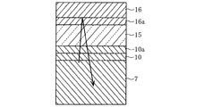
図1(A)に、第1の実施例による半導体発光素子の断面図を示し、図1(B)に、その平面図を示す。図1(B)の一点鎖線A1−A1における断面が図1(A)に対応する。サファイアからなる下地基板1の上に、初期核形成層2、n型コンタクト層3、n型クラッド層4、発光層5、p型クラッド層6、p型コンタクト層7がこの順番に積層されている。これらの層は、InxAlyGazN(x+y+z=1)等の窒化物化合物半導体で形成されている。
FIG. 1A shows a cross-sectional view of the semiconductor light emitting device according to the first embodiment, and FIG. 1B shows a plan view thereof. A cross section taken along one-dot chain line A1-A1 in FIG. 1B corresponds to FIG. On an
基板面内の一部の第1の領域25において、p型コンタクト層7からn型コンタクト層3の表層部までの各層がエッチングされ、n型コンタクト層3の一部が表出している。
In a part of the
p型コンタクト層7の上に、p側オーミック電極10が形成されている。p側オーミック電極10は白金(Pt)で形成され、その厚さは約5nmである。第1の領域25内のn型コンタクト層3の表面上に、n側オーミック電極11が形成されている。n側オーミック電極11は、厚さ約3nmのAl層と厚さ約100nmのロジウム(Rh)層との2層構造を有する。p側オーミック電極10及びn側オーミック電極11は、それぞれp型コンタクト層7及びn型コンタクト層3にオーミック接触する。
A p-
p側オーミック電極10及びn側オーミック電極11の上に、Ti、Ni、W、Mo等からなる厚さ0.3〜3nmの接着層(図示せず)が形成されている。接着層は、その上に堆積される絶縁膜15の密着性を高めることができる。
On the p-
p側オーミック電極10、n側オーミック電極11を覆うように、基板上に絶縁膜15が形成されている。絶縁膜15は、例えば酸化シリコンで形成され、その厚さは約300nmである。絶縁膜15に、開口15a及び15bが形成されている。開口15aの底面にp側オーミック電極10の表面の一部が露出し、開口15bの底面にn側オーミック電極11の表面の一部が露出する。
An insulating
絶縁膜15の上に反射膜16が形成されている。反射膜16は、p側オーミック電極10と重なる領域から、第1の領域25内のn側オーミック電極11上まで延在し、開口15bの底面に露出したn側オーミック電極11に電気的に接続される。反射膜16は銀(Ag)で形成され、その厚さは約200nmである。
A
絶縁膜15と反射膜16との間に、Ti、Ni、Al、W、Mo等からなる厚さ0.3〜3nmの接着層(図示せず)が挿入されている。この接着層は、絶縁膜15と反射膜16との密着性を高める。反射膜16の上にも、同様の接着層(図示せず)が形成されている。この接着層は、その上に形成される保護膜17の密着性を高める。上側の接着層の厚さは、例えば10nmとする。
An adhesive layer (not shown) made of Ti, Ni, Al, W, Mo or the like and having a thickness of 0.3 to 3 nm is inserted between the insulating
開口15aの底面に露出したp側オーミック電極10の上にp側パッド電極20が形成され、開口15bの底面に露出したn側オーミック電極11の上にn側パッド電極21が形成されている。p側パッド電極20及びn側パッド電極21は、Ti/Pt/Au/(Pt/Au)nの多層構造を有する。ここでnは、Pt層とAu層との2層の繰り返し回数を示す。最も下に配置されたTi層の厚さは例えば3nmであり、Pt層とAu層との各々の厚さは例えば100nmである。繰り返し回数nは、例えば2である。なお、繰り返し回数nは、成膜の手間及び材料の使用量の観点から、1〜5とすることが好ましい。なお、フリップチップボンディングを行う場合には、n側パッド電極21の基板側から3層目のAu層の厚さを100nm〜1000nmとし、n側パッド電極21の上面の高さを、p側パッド電極20の上面の高さに揃えることが好ましい。
A p-
p側パッド電極20及びn側パッド電極21の上に、Ti、Ni、Al、W、Mo等からなる厚さ0.3〜3nmの接着層(図示せず)が形成されている。この接着層は、その上に形成される保護膜17の密着性を高める。
On the p-
反射膜16、パッド電極20、21を覆うように、保護膜17が形成されている。保護膜17は酸化シリコンで形成され、その厚さは100〜300nm、望ましくは約200nmである。保護膜17に、開口17a及び17bが形成されている。開口17a及び17bの底面に、それぞれp側パッド電極20及びn側パッド電極21の上面が露出する。
A
図1(B)に示したように、1つの半導体発光素子の平面形状は、例えば一辺が300μmの正方形である。第1の領域25は、この正方形の一つの頂点を含み、その頂点の近傍の領域で構成される。その形状は、例えば一つの頂点を中心とした中心角90°の扇形である。p側オーミック電極10は、第1の領域25を除く領域に配置され、半導体発光素子の表面の大部分を占める。p側パッド電極20は、第1の領域25に含まれる頂点とは反対側の頂点の近傍に配置されている。反射膜16は、p側パッド電極20が配置された領域を除き、半導体発光素子の表面の大部分を占める。
As shown in FIG. 1B, the planar shape of one semiconductor light emitting element is, for example, a square having a side of 300 μm. The
次に、第1の実施例による半導体発光素子の製造方法について説明する。サファイアからなる下地基板1上の初期核形成層2からp型コンタクト層7までの各層は、例えば有機金属気相エピタキシャル成長(MOVPE)または分子線エピタキシャル成長(MBE)等により形成される。p型コンタクト層7まで形成した後、基板表面を洗浄し、電子ビーム蒸着及びリフトオフ法を用いてp側オーミック電極10及びその上の接着層を形成する。
Next, a method for manufacturing the semiconductor light emitting device according to the first embodiment will be described. Each layer from the
第1の領域25に対応する開口が形成されたレジストパターンをマスクとして用い、反応性イオンエッチングにより、n型コンタクト層3の表層部までエッチングし、n型コンタクト層3の一部を露出させる。エッチング後、マスクとして用いたレジストパターンを除去する。n型コンタクト層3の露出した表面上に、電子ビーム蒸着及びリフトオフ法を用いてn側オーミック電極11を形成する。
Using the resist pattern in which the opening corresponding to the
なお、n型コンタクト層3の表面の一部を露出させた後に、p側オーミック電極10及びn側オーミック電極11を形成してもよい。
Note that the p-
スパッタリングにより絶縁膜15を形成する。絶縁膜15に、開口15a及び15bを形成する。なお、リフトオフ法を用いて開口15a及び15bを形成してもよい。電子ビーム蒸着とリフトオフ法を用いて、下側の接着層、反射膜16及び上側の接着層を形成する。反射膜16と、開口15aの底面に露出したp側オーミック電極10とが短絡されないように、反射膜16の縁を開口15aの縁から1μm以上、望ましくは5μm程度後退させておく。また、開口15bの底面に露出したn側オーミック電極11に電気的に接続されるように、反射膜16と開口15bとの重なり幅を3〜5μm程度確保しておく。これにより、反射膜16は、p側オーミック電極10には接続されず、n側オーミック電極11に電気的に接続されることになる。
An insulating
電子ビーム蒸着とリフトオフ法を用いて、p側パッド電極20、n側パッド電極21、及びその上の接着層を形成する。p側パッド電極20は、その外周が開口15aの縁よりもやや内側に配置されるように形成することが好ましい。なお、p側パッド電極20が反射膜16に接触しなければ、p側パッド電極20の外周近傍が絶縁膜15に重なってもよい。
The p-
スパッタリングにより保護膜17を形成する。その後、保護膜17に開口17a及び17bを形成する。なお、リフトオフ法を用いて開口17a及び17bを形成してもよい。開口17aの底面にp側パッド電極20の表面が露出し、開口17bの底面にn側パッド電極21の表面が露出する。
A
下地基板1の裏面を研削及び研磨し、下地基板1の厚さを約100μmまで薄くする。なお、下地基板1の厚さを60μm〜210μmとしてもよい。スクライビング及びブレーキングを行い、発光素子単位に分離する。分離された発光素子は、種々の形態で利用される。例えば、サブマウント基板にフリップチップボンディングされる。その他に、下地基板1を透明接着剤で導光板に貼り付け、p側パッド電極20及びn側パッド電極21を、導光板に設けられた配線に金線で接続してもよい。
The back surface of the
n型クラッド層4、発光層5、及びp型クラッド層6の積層構造に順方向電圧を印加することにより、発光層5で発光が生ずる。発光層5で発生した光は、下地基板1を透過して外部に放射される。発光層5で発生し、p型クラッド層6の方へ伝搬する光は、p側オーミック電極10及び絶縁膜15を透過し、反射膜16で下地基板1側へ反射され、下地基板1を透過して外部に放射される。
When a forward voltage is applied to the laminated structure of the n-
水分の存在下で電界を印加したときに、陽極でAgが溶解することが、Agのマイグレーションの原因になっていると考えられる。上記第1の実施例では、Agで形成された反射膜16が陰極(n側オーミック電極11)に接続されているため、Agの溶解が生じない。このため、Agのマイグレーションを抑制することができる。
When an electric field is applied in the presence of moisture, the dissolution of Ag at the anode is considered to cause the migration of Ag. In the first embodiment, since the
図2に、上記第1の実施例による半導体発光素子の寿命評価試験の結果を示す。横軸は経過時間を単位「時間」で表し、縦軸は発光出力を相対目盛で表す。比較例として、図1(A)に示したp側オーミック電極10をAgで形成し、p側オーミック電極10が反射膜を兼ねる構造の半導体発光素子の寿命評価試験の結果も示す。図中の黒四角記号が第1の実施例による半導体発光素子の発光出力の経時変化を示し、黒丸記号が比較例の半導体発光素子の発光出力の経時変化を示す。なお、寿命評価試験では、半導体発光素子をサブマウント基板にフリップチップボンディングし、大気中で発光させて発光出力を測定した。発光波長は405nmであった。
FIG. 2 shows the result of the life evaluation test of the semiconductor light emitting device according to the first embodiment. The horizontal axis represents the elapsed time in the unit “time”, and the vertical axis represents the light emission output in a relative scale. As a comparative example, the results of a life evaluation test of a semiconductor light emitting device having a structure in which the p-
比較例による半導体発光素子の発光出力は、数十時間で急激に低下しているが、実施例による半導体発光素子の発光出力は、1000時間経過してもほとんど低下していない。このように、Agからなる反射膜16を陰極に接続することにより、半導体発光素子の長寿命化を図ることができる。
The light emission output of the semiconductor light emitting device according to the comparative example is rapidly reduced in several tens of hours, but the light emission output of the semiconductor light emitting device according to the example is hardly lowered even after 1000 hours. As described above, the life of the semiconductor light emitting device can be extended by connecting the
上記第1の実施例では、p側オーミック電極10をPtで形成したが、発光層5の発光波長域の光を透過させ、p型コンタクト層7とオーミック接触が得られる他の導電材料で形成してもよい。使用可能な材料として、例えばロジウム(Rh)、パラジウム(Pd)等が挙げられる。その他に、Pt層とRh層との2層構造、またはNi層とAu層との2層構造にしてもよい。Ni層とAu層との2層構造とする場合には、オーミック接触を得るために、成膜後に熱処理を行う必要がある。また、AuとNiの酸化物とで構成された透光性酸化膜を用いることもできる。この場合には、成膜後に、酸化性雰囲気中で熱処理を行う必要がある。
In the first embodiment, the p-
また、上記第1の実施例では、n側オーミック電極11をAl層とRh層との2層構造(Al/Rh構造)としたが、n型コンタクト層3とオーミック接触可能な他の構成としてもよい。例えば、Al/Pt構造、Al/Ir構造、Al/Pd構造、Ti/Al構造、V/Al構造としてもよい。Ti/Al構造、またはV/Al構造を採用する場合には、オーミック接触を得るために、成膜後に熱処理を行う必要がある。
In the first embodiment, the n-
上記第1の実施例では、絶縁膜15を酸化シリコンで形成したが、発光層5の発光波長域の光を透過させる他の絶縁材料で形成していもよい。例えば、絶縁膜15の材料として、酸化チタン(TiO2)、酸化タンタル(Ta2O5)、アルミナ(Al2O3)、酸化ジルコニウム(ZrO2)、酸化ハフニウム(HfO2)等の酸化物、ポリイミド等の耐熱性有機高分子材料等を用いることができる。
In the first embodiment, the insulating
上記実施例ではp側パッド電極20をTi/Pt/Au/(Pt/Au)nの多層構造としたが、その他にTi/Rh/Au/(Pt/Au)nの多層構造、またはNi/Rh/Au/(Pt/Au)nの多層構造としてもよい。
最下層のTi層またはNi層の厚さは、例えば0.3〜1nmとする。その上のRh層、Pt層、Au層の各々の厚さは100nmとする。また、繰り返し回数nは1〜5とする。このような多層構造とすることにより、p側パッド電極20に反射膜としての機能を持たせ、光の取り出し効率を高めることができる。
In the above embodiment, the p-
The thickness of the lowermost Ti layer or Ni layer is, for example, 0.3 to 1 nm. The thickness of each of the Rh layer, Pt layer, and Au layer thereon is 100 nm. The number of repetitions n is 1 to 5. With such a multilayer structure, the p-
上記実施例では反射膜16をAgで形成したが、Agを主成分として含む合金で形成してもよい。反射膜16の厚さは、発光層5で発生した光を透過させないために、80nm以上とすることが好ましい。また、反射膜16を、Ag以外のマイグレーションの生じやすい金属で形成する場合にも、マイグレーション抑制効果が得られるであろう。特に、反射膜16を、p側オーミック電極10よりもマイグレーションの生じ易い金属で形成する場合に有効である。
In the above embodiment, the
上記実施例では、保護膜17を酸化シリコンで形成したが、その他の絶縁材料、例えば酸化チタン(TiO2)、酸化タンタル(Ta2O5)、アルミナ(Al2O3)、酸化ジルコニウム(ZrO2)、酸化ハフニウム(HfO2)等の酸化物、ポリイミド等の耐熱性有機高分子材料等で形成してもよい。
In the above embodiment, the
反射膜16の表面上に、Agよりもイオン化傾向の大きなAl等の金属からなる導電層を形成してもよい。イオン化傾向の差を利用した異種金属接合を併用することにより、電極間に通電しない状態においても、反射膜16の電気腐食を抑制することができる。
A conductive layer made of a metal such as Al, which has a higher ionization tendency than Ag, may be formed on the surface of the
上記第1の実施例では、p側オーミック電極10、絶縁膜15、及び反射膜16が多層反射膜を構成している。反射率は、これらの膜の厚さに依存する。金属薄膜及び誘電体膜で構成される多層膜の反射率を高くする好適条件を、実験により求めることは困難である。このため、シミュレーションにより、多層反射膜の反射率の膜厚依存性を評価した。以下、シミュレーションによる評価結果について説明する。
In the first embodiment, the p-
図3に、シミュレーションに用いた多層反射膜のモデルを示す。GaNからなるコンタクト層7の上に、Ptからなるp側オーミック電極10、Tiからなる接着層10a、SiO2からなる絶縁膜15、Tiからなる接着層16a、Agからなる反射膜16がこの順番に積層されている。コンタクト層7から反射膜16へ進む波長460nmの光の反射率をしミュレーションにより求めた。
FIG. 3 shows a model of the multilayer reflective film used in the simulation. On the
図4に、p側オーミック電極10の厚さと反射率との関係を示す。横軸はp側オーミック電極10の厚さを単位「nm」で表し、縦軸は反射率を単位「%」で表す。接着層10a、絶縁膜15、接着層16a、及び反射膜16の厚さは、それぞれ0.3nm、285nm、0.3nm、及び200nmとした。p側オーミック電極10の厚さが7nm以下の領域では反射率はほとんど膜厚の影響を受けず、厚さ7nm以上の領域では、膜厚の増加に伴って反射率が低下している。
FIG. 4 shows the relationship between the thickness of the p-
図5に、反射膜16の厚さと反射率との関係を示す。横軸は反射膜16の厚さを単位「nm」で表し、縦軸は反射率を単位「%」で表す。p側オーミック電極10、接着層10a、絶縁膜15、及び接着層16aの厚さは、それぞれ5nm、0.3nm、285nm、及び0.3nmとした。反射膜16が厚くなるに従って反射率が大きくなり、膜厚が80nm付近で反射率が飽和することがわかる。この結果から、反射膜16の厚さを80nm以上にすることが好ましいことがわかる。
FIG. 5 shows the relationship between the thickness of the
図6に、絶縁膜15の厚さと反射率との関係を示す。横軸は絶縁膜15の厚さを単位「nm」で表し、縦軸は反射率を単位「%」で表す。接着層10a、接着層16a、及び反射膜16の厚さは、それぞれ0.3nm、0.3nm、及び200nmとした。図中の3本の曲線は、p側オーミック電極10の厚さが3nm、5nm、及び8nmの場合の反射率を示す。反射率は、絶縁膜15の厚さの変動に従って周期的に変動する。絶縁膜15の厚さが約130nm、286nm、及び440nmの近傍で反射率が極大値を示している。
FIG. 6 shows the relationship between the thickness of the insulating
反射率が極小値を示す位置における反射率は、p側オーミック電極10が厚くなるに従って低下することがわかる。絶縁膜15の厚さが変動した時の反射率の低下を抑制するために、p側オーミック電極10を薄くすることが好ましい。ところが、薄くしすぎると、p型コンタクト層7に均一にキャリアを注入するという電極本来の目的を達成できなくなる。高反射率及びキャリアの均一な注入の両方の要請を満たすために、p側オーミック電極10の厚さを1nm〜15nmとすることが好ましく、3nm〜8nmとすることがより好ましい。また、p側オーミック電極10の厚さを1〜5nmと薄くし、その上に、PtまたはRhからなるメッシュ状の補助電極を設けてもよい。このメッシュを構成する1本の電極の幅を、例えば2〜5μmとし、電極の間隔を、例えば10〜15nmとすればよい。
It can be seen that the reflectance at the position where the reflectance exhibits a minimum value decreases as the p-
シミュレーションからは、絶縁膜15の厚さが約286nmときに反射率が極大値を示すことがわかったが、実際に評価用試料を作製して反射率を測定したところ、絶縁膜15の厚さが300nm近傍で反射率が極大値を示した。実験で得られた絶縁膜15の最適膜厚が、シミュレーションで得られた絶縁膜15の最適膜厚からずれたのは、シミュレーションで使用した各膜の光学特性と、実際に形成された各膜の光学特性とが正確には一致しないためと考えられる。絶縁性の確保及びエッチング時間等の観点から、絶縁膜15の厚さを100〜600nmとすることが好ましく、200〜400nmとすることがより好ましい。
From the simulation, it has been found that the reflectance shows a maximum value when the thickness of the insulating
図7及び図8に、絶縁膜15の厚さと反射率との関係を、種々の波長について示す。横軸は絶縁膜15の厚さを単位「nm」で表し、縦軸は反射率を単位「%」で表す。p側オーミック電極10、接着層10a、接着層16a、及び反射膜16の厚さは、それぞれ5nm、0.3nm、0.3nm、及び200nmとした。図7及び図8に示した複数の曲線の各々に付した数値は、反射すべき光の波長を示す。
7 and 8 show the relationship between the thickness of the insulating
反射すべき光の波長が変わると、反射率が極大値を示す絶縁膜15の厚さが変化する。絶縁膜15は、発光層で発生する光の波長に応じて、反射率が極大値を示す近傍の厚さとすることが好ましい。
When the wavelength of the light to be reflected changes, the thickness of the insulating
以上、シミュレーションを行うことにより、反射率を大きくするための膜厚の条件を求めたが、実際には、各膜の成膜方法により、膜の屈折率や消衰係数がいくらか異なる。また、反射率は、膜の表面粗さにも影響される。このため、各膜の最適膜厚は、シミュレーションで得られた最適膜厚を参考にして、膜厚の異なる複数の評価用試料を作製し、実際に反射率を測定することによって決定することが好ましい。シミュレーション結果は、評価用試料の各膜の厚さを決定する尺度になる。 As described above, the film thickness condition for increasing the reflectance is obtained by performing the simulation, but actually, the refractive index and extinction coefficient of the film are somewhat different depending on the film forming method. The reflectance is also affected by the surface roughness of the film. For this reason, the optimum film thickness of each film can be determined by referring to the optimum film thickness obtained by the simulation and preparing a plurality of evaluation samples having different film thicknesses and actually measuring the reflectance. preferable. The simulation result is a scale for determining the thickness of each film of the evaluation sample.
次に、実際に評価用試料を作製し、その反射率を測定した結果について説明する。評価用試料では、図3のp側コンタクト層7として、厚さ320μmのサファイア基板を用いた。p側オーミック電極10を、厚さ5nm、8nm、及び10nmのPt膜とし、接着層10a及び16aを厚さ0.3nmのTi膜とし、絶縁膜15を厚さ313nmのSiO2膜とし、反射膜16を厚さ200nmのAg膜とした。
Next, the result of actually producing an evaluation sample and measuring the reflectance will be described. In the sample for evaluation, a sapphire substrate having a thickness of 320 μm was used as the p-
サファイア基板の上に厚さ4〜8μm程度のGaN膜を形成すると、基板に反りが発生する。基板に反りが発生すると、反射率を測定するための入射光の入射角を正確に調整できなくなる。このため、測定用試料では、GaN層を形成しないサファイア基板を用いた。 When a GaN film having a thickness of about 4 to 8 μm is formed on a sapphire substrate, the substrate is warped. When the substrate is warped, the incident angle of incident light for measuring the reflectance cannot be adjusted accurately. For this reason, in the measurement sample, a sapphire substrate on which no GaN layer was formed was used.
図9に、反射率の測定結果を示す。横軸は波長を単位「nm」で表し、縦軸は反射率を単位「%」で表す。作製した試料においては、波長が350〜360nm、及び510〜520nmのときに、反射率が極大値を示した。種々の試料を作製して反射率を測定することにより、サファイア基板上に形成した多層反射膜の反射率と、GaN層上に形成した多層反射膜の反射率との関係を得ることができる。この関係を利用して、絶縁膜15の好ましい膜厚を予測することができる。
FIG. 9 shows the measurement results of the reflectance. The horizontal axis represents the wavelength in the unit “nm”, and the vertical axis represents the reflectance in the unit “%”. In the prepared sample, the reflectance showed the maximum value when the wavelength was 350 to 360 nm and 510 to 520 nm. By producing various samples and measuring the reflectance, the relationship between the reflectance of the multilayer reflective film formed on the sapphire substrate and the reflectance of the multilayer reflective film formed on the GaN layer can be obtained. By utilizing this relationship, a preferable film thickness of the insulating
次に、図10及び図11を参照して、第2の実施例による半導体発光素子について説明する。 Next, with reference to FIGS. 10 and 11, the semiconductor light emitting device according to the second embodiment will be described.
図10に、第2の実施例による半導体発光素子の平面図を示す。図1(B)に示した第1の実施例では、反射膜16が無地の膜であり、p側オーミック電極10の大部分の領域と重なっていた。第2の実施例では、反射膜16の代わりに、格子状の反射パターン16aが配置されている。その他の基本構成は、第1の実施例による半導体発光素子の構成と同様である。図10では、p側パッド電極20及びn側パッド電極21が、相互に対向する一対の辺の中央よりやや内側に配置されている場合が示されているが、図1(B)に示した第1の実施例の場合のように、矩形の頂点近傍に配置してもよい。
FIG. 10 is a plan view of a semiconductor light emitting device according to the second embodiment. In the first embodiment shown in FIG. 1B, the
第2の実施例による半導体発光素子においては、発光層で発生した光が支持基板を通して外部に放射されると共に、反射パターン16aの開口部を通して支持基板と反対側にも放射される。さらに、反射パターン16aで散乱され、半導体発光素子の側方にも光が放射される。
In the semiconductor light emitting device according to the second embodiment, the light generated in the light emitting layer is radiated to the outside through the support substrate, and is also radiated to the side opposite to the support substrate through the opening of the
図11に、第2の実施例による半導体発光素子を実装したランプの概略断面図を示す。凹部を有する金属製のフレーム30の凹部の底面に、図10に示した半導体発光素子28が、支持基板をフレーム側にして装着されている。フレーム30から陰極リード31が延びている。半導体発光素子28のn側パッド電極21が、金線35を介してフレーム30に接続されている。p側パッド電極20が金線36を介して陽極リード32に接続されている。
FIG. 11 is a schematic cross-sectional view of a lamp mounted with the semiconductor light emitting device according to the second embodiment. The semiconductor
フレーム30の凹部は、蛍光体37で埋め込まれている。半導体発光素子28は、蛍光体37に被覆されることになる。フレーム30、陰極リード31、及び陽極リード32が、封止樹脂38でモールドされている。
The concave portion of the frame 30 is embedded with a phosphor 37. The semiconductor
半導体発光素子28の下方(支持基板側)に放射された光は、フレーム30で反射され、蛍光体37に入射する。また、半導体発光素子28の側方や上方(支持基板の反対側)に放射された光も蛍光体37に入射する。蛍光体37は、光を受けることにより蛍光を発生させる。この蛍光が、樹脂モールド38の外部に放射される。
The light emitted below the semiconductor light emitting element 28 (on the support substrate side) is reflected by the frame 30 and enters the phosphor 37. Further, the light emitted to the side or upper side (opposite side of the support substrate) of the semiconductor
半導体発光素子28の下方、側方、及び上方に光が放射されるため、色むらを軽減することができる。
Since light is emitted below, to the side, and above the semiconductor
第2の実施例では、反射パターン16aを格子状にしたが、開口部を有し、光を散乱させるその他のパターンにしてもよい。例えば、縞状パターン、ハニカム状パターン等にしてもよい。
In the second embodiment, the
次に、図12(A)、図12(B)及び図13を参照して、第3の実施例による半導体発光素子について説明する。 Next, with reference to FIGS. 12A, 12B, and 13, a semiconductor light emitting device according to a third embodiment will be described.
図12(A)に、第3の実施例による半導体発光素子の断面図を示し、図12(B)にその平面図を示す。図12(B)の一点鎖線A12−A12における断面図が図12(A)に相当する。以下、図1(A)及び(B)に示した第1の実施例による半導体発光素子との相違点について説明する。 FIG. 12A shows a sectional view of a semiconductor light emitting device according to the third embodiment, and FIG. 12B shows a plan view thereof. A cross-sectional view taken along one-dot chain line A12-A12 in FIG. 12B corresponds to FIG. Hereinafter, differences from the semiconductor light emitting device according to the first embodiment shown in FIGS. 1A and 1B will be described.
第1の実施例では、n側パッド電極21がn側オーミック電極11の上に配置されていたが、第2の実施例では、n側パッド電極21がp側オーミック電極10の上方に配置され、反射膜16に接触している。保護膜17に形成された開口17a及び17bの底面に、それぞれp側パッド電極20及びn側パッド電極21が露出している。
In the first embodiment, the n-
図12(B)に示すように、n側オーミック電極11は、支持基板1の一つの辺の近傍に、その辺に沿って配置されている。p側パッド電極20は、n側オーミック電極11が沿う辺に対向する辺の一方の端部近傍に配置されている。反射膜16は、p側パッド電極20の配置されていない領域の大部分を占める。n側パッド電極21は、反射膜16とp側オーミック電極10との重なる領域のうち大部分を占める。
As shown in FIG. 12B, the n-
図13に、第3の実施例による半導体発光素子を実装したランプの概略断面図を示す。第3の実施例による半導体発光素子50が、サブマウント基板43にフリップチップボンディングされている。半導体発光素子50のp側パッド電極20及びn側パッド電極21が、それぞれサブマウント基板43上の陽極配線44及び陰極配線45に接続されている。サブマウント基板43がステム40に固定されている。ステム40に、陽極リード42及び陰極リード41が固定されている。陽極配線44が金線46を介して陽極リード42に接続され、陰極配線45が金線47を介して陰極リード41に接続されている。
FIG. 13 is a schematic cross-sectional view of a lamp on which the semiconductor light emitting device according to the third embodiment is mounted. The semiconductor
半導体発光素子50及びサブマウント基板43は、封止樹脂48により封止されている。半導体発光素子50の発光層で発生した光は、図12(A)に示した反射膜16で反射され、支持基板1及び封止樹脂48を透過して外部に放射される。
The semiconductor
第3の実施例による半導体発光素子においては、第1の実施例による半導体発光素子に比べて、n側パッド電極21が素子表面の広い領域を占める。この広いn側パッド電極21を介して、素子内で発生した熱がサブマウント基板43に効率的に流れる。このため、良好な放熱特性を確保することができる。
In the semiconductor light emitting device according to the third embodiment, the n-
次に、図14(A)及び図14(B)を参照して、第4の実施例による半導体発光素子について説明する。 Next, with reference to FIGS. 14A and 14B, a semiconductor light emitting element according to the fourth embodiment will be described.
図14(A)に、第4の実施例による半導体発光素子の断面図を示し、図14(B)に、その平面図を示す。図14(B)の一点鎖線A14−A14における断面図が図14(A)に相当する。第4の実施例においては、4つのn側オーミック電極11が、それぞれ正方形状の支持基板1の4つの辺に沿うように配置されている。反射膜16が、4つのn側オーミック電極11に接続される。p側パッド電極20を内包するように、反射膜16に開口16aが形成されている。開口16aを形成することにより、反射膜16とp側パッド電極20との短絡が回避される。
FIG. 14A shows a cross-sectional view of a semiconductor light emitting device according to the fourth embodiment, and FIG. 14B shows a plan view thereof. A cross-sectional view along dashed-dotted line A14-A14 in FIG. 14B corresponds to FIG. In the fourth embodiment, the four n-
第4の実施例では、4つのn側オーミック電極11が形成されているため、電極の接触面積を大きくすることができ、接触抵抗の低減を図ることが可能になる。また、4つのn側オーミック電極11を正方形の4つの辺に沿って配置することにより、基板面内における電流の偏りを少なくすることができる。
In the fourth embodiment, since the four n-
支持基板1の頂点近傍は、素子分離の際に欠け易い。このため、n側オーミック電極11は、支持基板1の頂点近傍まで延在させないことが好ましい。
The vicinity of the apex of the
また、第4の実施例では、n型クラッド層4からp型クラッド層7までの積層で構成されたメサ部の側面の全域が反射膜16で覆われている。このため、発光層5から側方に放射された光を効率的に支持基板1側に反射させることができ、光の取り出し効率を高めることができる。光の取り出し効率をより高めるために、メサ部の側面を傾斜させることが好ましい。例えば、メサ部の側面の傾斜角を60°以下にすることが好ましい。
Further, in the fourth embodiment, the entire side surface of the mesa portion formed by stacking from the n-
以下、メサ部の側面を傾斜させる方法の一例について説明する。通常のレジストパターンを形成する時は、フォトマスクをレジスト膜に接触させて露光を行なう。メサ部の側面を傾斜させる場合には、フォトマスクをレジスト膜から僅かに浮かせて露光を行なう。レジスト膜とフォトマスクとの間に間隙が形成されるため、フォトマスクのパターンのエッジ部分がぼけて転写される。レジスト膜を現像すると、側面が傾斜したレジストパターンが得られる。 Hereinafter, an example of a method for inclining the side surface of the mesa unit will be described. When a normal resist pattern is formed, exposure is performed by bringing a photomask into contact with the resist film. When the side surface of the mesa portion is inclined, exposure is performed with the photomask slightly lifted from the resist film. Since a gap is formed between the resist film and the photomask, the edge portion of the photomask pattern is blurred and transferred. When the resist film is developed, a resist pattern having an inclined side surface is obtained.
このレジストパターンをエッチングマスクとして、窒化物半導体層をドライエッチングすると、レジストパターン自体も徐々にエッチングされるため、レジストパターンの側面の傾きに対応して、窒化物半導体のメサ部の側面が傾斜する。 When the nitride semiconductor layer is dry-etched using this resist pattern as an etching mask, the resist pattern itself is also gradually etched. Therefore, the side surface of the mesa portion of the nitride semiconductor is inclined corresponding to the inclination of the side surface of the resist pattern. .
上記実施例では、反射膜16をn側オーミック電極11に接続したが、反射膜16を、p側オーミック電極10及びn側オーミック電極11のいずれにも接続せず、電気的にフローティング状態にしてもよい。フローティング状態の場合にも、図15(B)や図15(C)に示したように反射膜を陽極に接続する場合に比べて、マイグレーションを抑制することができる。
In the above embodiment, the
以上実施例に沿って本発明を説明したが、本発明はこれらに制限されるものではない。例えば、種々の変更、改良、組み合わせ等が可能なことは当業者に自明であろう。 Although the present invention has been described with reference to the embodiments, the present invention is not limited thereto. It will be apparent to those skilled in the art that various modifications, improvements, combinations, and the like can be made.
1 下地基板
2 初期核形成層
3 n型コンタクト層
4 n型クラッド層
5 発光層
6 p型クラッド層
7 p型コンタクト層
10 p側オーミック電極
10a、16a 接着層
11 n側オーミック電極
15 絶縁膜
16 反射膜
16a 反射パターン
17 保護膜
20 p側パッド電極
21 n側パッド電極
25 第1の領域
28、50 半導体発光素子
30 フレーム
31、41 陰極リード
32、42 陽極リード
35、36、46、47 金線
37 蛍光体
38、48 封止樹脂
40 ステム
43 サブマウント基板
44 陽極配線
45 陰極配線
DESCRIPTION OF
Claims (10)
前記第2の層の表面上に配置され、該第2の層に電気的に接続されたp側電極と、
前記p側電極を覆う絶縁膜と、
前記第1の領域において、前記第1の層に電気的に接続されたn側電極と、
前記絶縁膜の上に、前記p側電極と重なるように配置され、前記n側電極まで至り、該n側電極に電気的に接続され、銀を含む合金または銀で形成された反射膜と
を有する半導体発光素子。 a first layer made of an n-type nitride semiconductor; and a second layer made of a p-type nitride semiconductor disposed on the first layer, wherein the first layer and the second layer A light emitting stacked structure in which a light emitting region is defined between the first layer and the first layer on the surface of the first layer, wherein the second layer is removed and the first layer appears.
A p-side electrode disposed on the surface of the second layer and electrically connected to the second layer;
An insulating film covering the p-side electrode;
An n-side electrode electrically connected to the first layer in the first region;
A reflective film made of an alloy containing silver or silver that is disposed on the insulating film so as to overlap the p-side electrode, reaches the n-side electrode, and is electrically connected to the n-side electrode. A semiconductor light emitting device having the same.
前記第2の層の表面上に配置され、該第2の層に電気的に接続され、前記発光領域で発生した光を透過させるp側電極と、
前記p側電極を覆う絶縁膜と、
前記第1の領域において、前記第1の層に電気的に接続されたn側電極と、
前記絶縁膜の上に、前記p側電極と重なるように配置され、前記n側電極まで至り、該n側電極に電気的に接続され、前記発光領域で発生した光を反射する反射膜と
を有する半導体発光素子。 a first layer made of an n-type nitride semiconductor; and a second layer made of a p-type nitride semiconductor disposed on the first layer, wherein the first layer and the second layer A light emitting stacked structure in which a light emitting region is defined between the first layer and the first layer on the surface of the first layer, wherein the second layer is removed and the first layer appears.
A p-side electrode disposed on the surface of the second layer, electrically connected to the second layer, and transmitting light generated in the light emitting region;
An insulating film covering the p-side electrode;
An n-side electrode electrically connected to the first layer in the first region;
A reflective film that is disposed on the insulating film so as to overlap the p-side electrode, reaches the n-side electrode, is electrically connected to the n-side electrode, and reflects light generated in the light emitting region. A semiconductor light emitting device having the same.
前記n側電極の表面の一部の領域上に配置されたフリップチップボンディング用のn側パッドと
を有する請求項1〜6のいずれかに記載の半導体発光素子。 Furthermore, a p-side pad for flip chip bonding disposed on a partial region of the surface of the p-side electrode;
The device according to any one of claims 1 to 6 having an n-side pad for flip chip bonding that is disposed on a partial region of the surface of the n-side electrode.
前記反射膜のうち、前記第2の層と重なる部分の表面上に配置されたフリップチップボンディング用のn側パッドと
を有する請求項1〜6のいずれかに記載の半導体発光素子。 Furthermore, a p-side pad for flip chip bonding disposed on a partial region of the surface of the p-side electrode;
Wherein the reflected film, the semiconductor light-emitting device according to any one of claims 1 to 6 having an n-side pad for the flip chip bonding that is disposed on a surface of a portion overlapping the second layer.
さらに、前記反射膜で散乱された光が入射することにより蛍光を発生する蛍光体を有する請求項1〜6のいずれかに記載の半導体発光素子。 The reflective film has a planar shape that scatters light emitted from the light emitting region and traveling toward the reflective film,
Furthermore, the semiconductor light-emitting device according to any one of claims 1 to 6 having a fluorescent material in which the light scattered by the reflective film to generate fluorescence by incident.
Priority Applications (4)
| Application Number | Priority Date | Filing Date | Title |
|---|---|---|---|
| JP2004095217A JP4330476B2 (en) | 2004-03-29 | 2004-03-29 | Semiconductor light emitting device |
| EP04024366.9A EP1583159B1 (en) | 2004-03-29 | 2004-10-13 | Semiconductor light emitting device capable of suppressing silver migration of reflection film made of silver |
| US10/968,761 US7141825B2 (en) | 2004-03-29 | 2004-10-19 | Semiconductor light emitting device capable of suppressing silver migration of reflection film made of silver |
| TW094107302A TWI262610B (en) | 2004-03-29 | 2005-03-10 | Semiconductor light emitting device capable of suppressing silver migration of reflection film made of silver |
Applications Claiming Priority (1)
| Application Number | Priority Date | Filing Date | Title |
|---|---|---|---|
| JP2004095217A JP4330476B2 (en) | 2004-03-29 | 2004-03-29 | Semiconductor light emitting device |
Related Child Applications (1)
| Application Number | Title | Priority Date | Filing Date |
|---|---|---|---|
| JP2009098265A Division JP5021693B2 (en) | 2009-04-14 | 2009-04-14 | Semiconductor light emitting device |
Publications (3)
| Publication Number | Publication Date |
|---|---|
| JP2005302747A JP2005302747A (en) | 2005-10-27 |
| JP2005302747A5 JP2005302747A5 (en) | 2007-05-17 |
| JP4330476B2 true JP4330476B2 (en) | 2009-09-16 |
Family
ID=34879909
Family Applications (1)
| Application Number | Title | Priority Date | Filing Date |
|---|---|---|---|
| JP2004095217A Expired - Fee Related JP4330476B2 (en) | 2004-03-29 | 2004-03-29 | Semiconductor light emitting device |
Country Status (4)
| Country | Link |
|---|---|
| US (1) | US7141825B2 (en) |
| EP (1) | EP1583159B1 (en) |
| JP (1) | JP4330476B2 (en) |
| TW (1) | TWI262610B (en) |
Families Citing this family (113)
| Publication number | Priority date | Publication date | Assignee | Title |
|---|---|---|---|---|
| US9000461B2 (en) * | 2003-07-04 | 2015-04-07 | Epistar Corporation | Optoelectronic element and manufacturing method thereof |
| US9142740B2 (en) | 2003-07-04 | 2015-09-22 | Epistar Corporation | Optoelectronic element and manufacturing method thereof |
| US10686106B2 (en) | 2003-07-04 | 2020-06-16 | Epistar Corporation | Optoelectronic element |
| US20060108672A1 (en) * | 2004-11-24 | 2006-05-25 | Brennan John M | Die bonded device and method for transistor packages |
| WO2006098545A2 (en) | 2004-12-14 | 2006-09-21 | Seoul Opto Device Co., Ltd. | Light emitting device having a plurality of light emitting cells and package mounting the same |
| JP4967243B2 (en) * | 2005-03-08 | 2012-07-04 | 三菱化学株式会社 | GaN-based light emitting diode and light emitting device |
| EP2280430B1 (en) | 2005-03-11 | 2020-01-01 | Seoul Semiconductor Co., Ltd. | LED package having an array of light emitting cells coupled in series |
| JP4956902B2 (en) * | 2005-03-18 | 2012-06-20 | 三菱化学株式会社 | GaN-based light emitting diode and light emitting device using the same |
| WO2007029859A1 (en) * | 2005-09-08 | 2007-03-15 | Showa Denko K.K. | Electrode for semiconductor light emitting device |
| JP4947954B2 (en) * | 2005-10-31 | 2012-06-06 | スタンレー電気株式会社 | Light emitting element |
| JP4777757B2 (en) * | 2005-12-01 | 2011-09-21 | スタンレー電気株式会社 | Semiconductor light emitting device and manufacturing method thereof |
| JP4952884B2 (en) * | 2006-01-24 | 2012-06-13 | ソニー株式会社 | Semiconductor light emitting device and semiconductor light emitting device assembly |
| KR101235460B1 (en) * | 2006-02-14 | 2013-02-20 | 엘지이노텍 주식회사 | Side-View Type Light Emitting Diode and Manufacturing Method thereof |
| JP5153082B2 (en) * | 2006-03-24 | 2013-02-27 | 三洋電機株式会社 | Semiconductor element |
| JP5162909B2 (en) * | 2006-04-03 | 2013-03-13 | 豊田合成株式会社 | Semiconductor light emitting device |
| US7573074B2 (en) * | 2006-05-19 | 2009-08-11 | Bridgelux, Inc. | LED electrode |
| US7737455B2 (en) * | 2006-05-19 | 2010-06-15 | Bridgelux, Inc. | Electrode structures for LEDs with increased active area |
| US20090086491A1 (en) | 2007-09-28 | 2009-04-02 | Ruud Lighting, Inc. | Aerodynamic LED Floodlight Fixture |
| US9028087B2 (en) | 2006-09-30 | 2015-05-12 | Cree, Inc. | LED light fixture |
| US9212812B2 (en) | 2013-02-11 | 2015-12-15 | Cree, Inc. | LED light fixture with integrated light shielding |
| US9222632B2 (en) | 2013-01-31 | 2015-12-29 | Cree, Inc. | LED lighting fixture |
| US7686469B2 (en) | 2006-09-30 | 2010-03-30 | Ruud Lighting, Inc. | LED lighting fixture |
| US8878245B2 (en) * | 2006-11-30 | 2014-11-04 | Cree, Inc. | Transistors and method for making ohmic contact to transistors |
| US7609004B2 (en) * | 2007-04-05 | 2009-10-27 | World Properties, Inc. | Eliminating silver migration in EL lamps |
| US9484499B2 (en) * | 2007-04-20 | 2016-11-01 | Cree, Inc. | Transparent ohmic contacts on light emitting diodes with carrier substrates |
| US8092042B2 (en) | 2007-05-03 | 2012-01-10 | Ruud Lighting, Inc. | Shield member in LED apparatus |
| JP2008305857A (en) * | 2007-06-05 | 2008-12-18 | Mitsubishi Electric Corp | Optical semiconductor device |
| JP2009059970A (en) * | 2007-08-31 | 2009-03-19 | Seiwa Electric Mfg Co Ltd | Semiconductor light-emitting element and method for fabricating semiconductor light-emitting element |
| US8536584B2 (en) * | 2007-11-14 | 2013-09-17 | Cree, Inc. | High voltage wire bond free LEDS |
| US9634191B2 (en) | 2007-11-14 | 2017-04-25 | Cree, Inc. | Wire bond free wafer level LED |
| US9754926B2 (en) * | 2011-01-31 | 2017-09-05 | Cree, Inc. | Light emitting diode (LED) arrays including direct die attach and related assemblies |
| US9660153B2 (en) | 2007-11-14 | 2017-05-23 | Cree, Inc. | Gap engineering for flip-chip mounted horizontal LEDs |
| US8368100B2 (en) * | 2007-11-14 | 2013-02-05 | Cree, Inc. | Semiconductor light emitting diodes having reflective structures and methods of fabricating same |
| US8575633B2 (en) * | 2008-12-08 | 2013-11-05 | Cree, Inc. | Light emitting diode with improved light extraction |
| US9640737B2 (en) | 2011-01-31 | 2017-05-02 | Cree, Inc. | Horizontal light emitting diodes including phosphor particles |
| US8026527B2 (en) * | 2007-12-06 | 2011-09-27 | Bridgelux, Inc. | LED structure |
| WO2009113659A1 (en) * | 2008-03-13 | 2009-09-17 | 昭和電工株式会社 | Semiconductor light-emitting device and method for manufacturing the same |
| JP2013038450A (en) * | 2008-03-26 | 2013-02-21 | Panasonic Corp | Semiconductor light-emitting element and light device using the same |
| US7637630B2 (en) * | 2008-04-22 | 2009-12-29 | Ruud Lighting, Inc. | Integrated shield-gasket member in LED apparatus |
| DE102008024327A1 (en) * | 2008-05-20 | 2009-11-26 | Osram Opto Semiconductors Gmbh | Optoelectronic semiconductor chip with a reflective layer |
| US8384115B2 (en) * | 2008-08-01 | 2013-02-26 | Cree, Inc. | Bond pad design for enhancing light extraction from LED chips |
| TW201021240A (en) * | 2008-11-24 | 2010-06-01 | Harvatek Corp | Wafer level LED package structure for increasing light-emitting efficiency |
| US8741715B2 (en) * | 2009-04-29 | 2014-06-03 | Cree, Inc. | Gate electrodes for millimeter-wave operation and methods of fabrication |
| US7977132B2 (en) * | 2009-05-06 | 2011-07-12 | Koninklijke Philips Electronics N.V. | Extension of contact pads to the die edge via electrical isolation |
| JP5244703B2 (en) | 2009-05-22 | 2013-07-24 | 昭和電工株式会社 | LIGHT EMITTING DIODE, LIGHT EMITTING DIODE LAMP, AND LIGHTING DEVICE |
| WO2011016201A1 (en) * | 2009-08-06 | 2011-02-10 | パナソニック株式会社 | Light-emitting element and light-emitting device |
| JP5543164B2 (en) * | 2009-09-25 | 2014-07-09 | 豊田合成株式会社 | Light emitting element |
| JP5414579B2 (en) * | 2009-11-19 | 2014-02-12 | 株式会社東芝 | Semiconductor light emitting device |
| JP5793292B2 (en) * | 2010-02-17 | 2015-10-14 | 豊田合成株式会社 | Semiconductor light emitting device |
| JP5761171B2 (en) * | 2010-02-26 | 2015-08-12 | 日亜化学工業株式会社 | Nitride semiconductor light emitting device and manufacturing method thereof |
| KR101039948B1 (en) * | 2010-04-23 | 2011-06-09 | 엘지이노텍 주식회사 | Light emitting device, method for fabricating the light emitting device and light emitting device package |
| JP5414627B2 (en) * | 2010-06-07 | 2014-02-12 | 株式会社東芝 | Semiconductor light emitting device and manufacturing method thereof |
| JP5659966B2 (en) * | 2010-06-29 | 2015-01-28 | 日亜化学工業株式会社 | Semiconductor device and manufacturing method thereof |
| JP2012028381A (en) * | 2010-07-20 | 2012-02-09 | Sharp Corp | Semiconductor light emitting device and method of manufacturing the same |
| JP5633477B2 (en) | 2010-08-27 | 2014-12-03 | 豊田合成株式会社 | Light emitting element |
| US9070851B2 (en) | 2010-09-24 | 2015-06-30 | Seoul Semiconductor Co., Ltd. | Wafer-level light emitting diode package and method of fabricating the same |
| JP5630384B2 (en) * | 2010-09-28 | 2014-11-26 | 豊田合成株式会社 | Group III nitride semiconductor light emitting device manufacturing method |
| US8455882B2 (en) | 2010-10-15 | 2013-06-04 | Cree, Inc. | High efficiency LEDs |
| KR101189081B1 (en) | 2010-12-16 | 2012-10-10 | 엘지이노텍 주식회사 | Wafer substrate bonding structure, light emitting diode comprising the same and manufacturing method thereof |
| JP2012146926A (en) | 2011-01-14 | 2012-08-02 | Rohm Co Ltd | Light-emitting element, light-emitting element unit and light-emitting element package |
| US9831220B2 (en) | 2011-01-31 | 2017-11-28 | Cree, Inc. | Light emitting diode (LED) arrays including direct die attach and related assemblies |
| US9673363B2 (en) | 2011-01-31 | 2017-06-06 | Cree, Inc. | Reflective mounting substrates for flip-chip mounted horizontal LEDs |
| US9053958B2 (en) | 2011-01-31 | 2015-06-09 | Cree, Inc. | Light emitting diode (LED) arrays including direct die attach and related assemblies |
| US9401103B2 (en) | 2011-02-04 | 2016-07-26 | Cree, Inc. | LED-array light source with aspect ratio greater than 1 |
| US8569889B1 (en) * | 2011-02-09 | 2013-10-29 | Nlight Photonics Corporation | Nano thick Pt metallization layer |
| JP5754173B2 (en) * | 2011-03-01 | 2015-07-29 | ソニー株式会社 | Light emitting unit and display device |
| JP5541260B2 (en) * | 2011-03-21 | 2014-07-09 | 豊田合成株式会社 | Group III nitride semiconductor light emitting device |
| JP5541261B2 (en) * | 2011-03-23 | 2014-07-09 | 豊田合成株式会社 | Group III nitride semiconductor light emitting device |
| JP5652373B2 (en) | 2011-03-24 | 2015-01-14 | 豊田合成株式会社 | Group III nitride semiconductor light emitting device manufacturing method |
| DE102011114865B4 (en) * | 2011-07-29 | 2023-03-02 | OSRAM Opto Semiconductors Gesellschaft mit beschränkter Haftung | Optoelectronic component and method for producing an optoelectronic component |
| JP5321656B2 (en) * | 2011-08-05 | 2013-10-23 | 三菱化学株式会社 | GaN-based light emitting diode and light emitting device |
| JP5304855B2 (en) * | 2011-08-12 | 2013-10-02 | 三菱化学株式会社 | GaN-based light emitting diode and light emitting device using the same |
| KR20130024089A (en) * | 2011-08-30 | 2013-03-08 | 엘지이노텍 주식회사 | Light emitting device |
| TWI473307B (en) * | 2011-10-13 | 2015-02-11 | Automotive Res & Testing Ct | A planar light source light emitting device having a reflective layer |
| TWI479694B (en) * | 2012-01-11 | 2015-04-01 | Formosa Epitaxy Inc | Light emitting diode wafers |
| KR101740531B1 (en) * | 2012-07-02 | 2017-06-08 | 서울바이오시스 주식회사 | Light Emitting Diode Module for Surface Mount Technology and Method of manufacturing the same |
| US9461212B2 (en) | 2012-07-02 | 2016-10-04 | Seoul Viosys Co., Ltd. | Light emitting diode module for surface mount technology and method of manufacturing the same |
| JP5900284B2 (en) * | 2012-10-25 | 2016-04-06 | 豊田合成株式会社 | Semiconductor light emitting element and light emitting device |
| JP5971090B2 (en) * | 2012-11-14 | 2016-08-17 | 豊田合成株式会社 | Semiconductor light emitting element and light emitting device |
| US9435519B2 (en) | 2013-01-31 | 2016-09-06 | Cree, Inc. | Light-fixture support assembly |
| KR102006390B1 (en) | 2013-03-11 | 2019-08-01 | 삼성전자주식회사 | Method of manufacturing Light Emitting diode package |
| DE102013103216A1 (en) * | 2013-03-28 | 2014-10-02 | Osram Opto Semiconductors Gmbh | Radiation emitting semiconductor chip |
| KR102085897B1 (en) * | 2013-06-10 | 2020-03-06 | 엘지이노텍 주식회사 | Light emitting device and light emitting device package |
| DE102013107531A1 (en) | 2013-07-16 | 2015-01-22 | Osram Opto Semiconductors Gmbh | Optoelectronic semiconductor chip |
| JP6215612B2 (en) | 2013-08-07 | 2017-10-18 | ソニーセミコンダクタソリューションズ株式会社 | LIGHT EMITTING ELEMENT, LIGHT EMITTING ELEMENT WAFER, AND ELECTRONIC DEVICE |
| CN104576857B (en) * | 2013-10-15 | 2017-07-04 | 上海工程技术大学 | A kind of high reflection layer flip LED chips structure and preparation method thereof |
| US10008635B2 (en) * | 2014-06-10 | 2018-06-26 | Semicon Light Co., Ltd. | Semiconductor light-emitting element |
| FR3023061B1 (en) * | 2014-06-27 | 2017-12-15 | Commissariat Energie Atomique | MESA STRUCTURE DIODE WITH SUBSTANTIALLY PLANE CONTACT SURFACE |
| USD826871S1 (en) | 2014-12-11 | 2018-08-28 | Cree, Inc. | Light emitting diode device |
| JP6827265B2 (en) * | 2015-01-05 | 2021-02-10 | シチズン電子株式会社 | LED light emitting device |
| CN107408606B (en) * | 2015-03-30 | 2019-12-13 | 索尼半导体解决方案公司 | light emitting element, light emitting unit, light emitting panel device, and method of driving light emitting panel device |
| KR20170003102A (en) * | 2015-06-30 | 2017-01-09 | 엘지이노텍 주식회사 | Light emitting device and light emitting device package comprising the same |
| CN104934514B (en) * | 2015-07-06 | 2018-06-22 | 天津宝坻紫荆科技有限公司 | A kind of composite insulation layer and preparation method |
| KR101744845B1 (en) * | 2015-09-30 | 2017-06-08 | 순천대학교 산학협력단 | Method for manufacturing light emitting diode and light emitting diode using the same |
| CN105226177B (en) * | 2015-10-13 | 2018-03-02 | 厦门市三安光电科技有限公司 | The eutectic electrode structure and flip LED chips of flip LED chips |
| JP6617875B2 (en) * | 2015-12-10 | 2019-12-11 | ウシオ電機株式会社 | LED element and manufacturing method thereof |
| JP7266961B2 (en) | 2015-12-31 | 2023-05-01 | 晶元光電股▲ふん▼有限公司 | light emitting device |
| CN205944139U (en) | 2016-03-30 | 2017-02-08 | 首尔伟傲世有限公司 | Ultraviolet ray light -emitting diode spare and contain this emitting diode module |
| CN105655463B (en) * | 2016-04-11 | 2018-09-18 | 杭州士兰明芯科技有限公司 | A kind of LED structure and preparation method thereof |
| DE102016106831A1 (en) * | 2016-04-13 | 2017-10-19 | Osram Opto Semiconductors Gmbh | Optoelectronic semiconductor chip |
| KR102532743B1 (en) * | 2016-12-06 | 2023-05-16 | 쑤저우 레킨 세미컨덕터 컴퍼니 리미티드 | light emitting element |
| CN106684223B (en) * | 2016-12-07 | 2019-04-12 | 华灿光电(浙江)有限公司 | A kind of chip of light emitting diode and preparation method thereof |
| WO2018164371A1 (en) | 2017-03-08 | 2018-09-13 | 엘지이노텍 주식회사 | Semiconductor device and semiconductor device package |
| KR102237158B1 (en) * | 2017-03-08 | 2021-04-07 | 엘지이노텍 주식회사 | Semiconductor device and semiconductor device package |
| WO2019051764A1 (en) * | 2017-09-15 | 2019-03-21 | 厦门市三安光电科技有限公司 | Microscopic light-emitting diode, and manufacturing method therefor |
| US20190237629A1 (en) * | 2018-01-26 | 2019-08-01 | Lumileds Llc | Optically transparent adhesion layer to connect noble metals to oxides |
| CN108417682B (en) * | 2018-03-22 | 2020-03-20 | 厦门市三安光电科技有限公司 | Micro light-emitting element and manufacturing method thereof |
| KR102495758B1 (en) * | 2018-08-10 | 2023-02-03 | 삼성전자주식회사 | Flip-chip light emitting diode, manufacturing method of flip-chip light emitting diode and display device including flip-chip light emitting diode |
| KR102300384B1 (en) * | 2019-10-17 | 2021-09-09 | 주식회사 피앤엘세미 | Light emitting diode and manufacturing method therof |
| JP7307662B2 (en) * | 2019-10-31 | 2023-07-12 | 日機装株式会社 | Semiconductor light emitting device and method for manufacturing semiconductor light emitting device |
| US11705534B2 (en) | 2020-12-01 | 2023-07-18 | Lumileds Llc | Methods of making flip chip micro light emitting diodes |
| US11955583B2 (en) | 2020-12-01 | 2024-04-09 | Lumileds Llc | Flip chip micro light emitting diodes |
| WO2024038686A1 (en) * | 2022-08-19 | 2024-02-22 | ソニーセミコンダクタソリューションズ株式会社 | Light-emitting device |
Family Cites Families (17)
| Publication number | Priority date | Publication date | Assignee | Title |
|---|---|---|---|---|
| US5291507A (en) * | 1991-05-15 | 1994-03-01 | Minnesota Mining And Manufacturing Company | Blue-green laser diode |
| US5889295A (en) * | 1996-02-26 | 1999-03-30 | Kabushiki Kaisha Toshiba | Semiconductor device |
| JP3447527B2 (en) * | 1996-09-09 | 2003-09-16 | 株式会社東芝 | Semiconductor light emitting device and method of manufacturing the same |
| JP3503439B2 (en) * | 1997-09-11 | 2004-03-08 | 日亜化学工業株式会社 | Nitride semiconductor device |
| JP3130292B2 (en) * | 1997-10-14 | 2001-01-31 | 松下電子工業株式会社 | Semiconductor light emitting device and method of manufacturing the same |
| US5952681A (en) * | 1997-11-24 | 1999-09-14 | Chen; Hsing | Light emitting diode emitting red, green and blue light |
| JPH11220171A (en) | 1998-02-02 | 1999-08-10 | Toyoda Gosei Co Ltd | Gallium nitride compound semiconductor device |
| US6936859B1 (en) * | 1998-05-13 | 2005-08-30 | Toyoda Gosei Co., Ltd. | Light-emitting semiconductor device using group III nitride compound |
| JP3531475B2 (en) * | 1998-05-22 | 2004-05-31 | 日亜化学工業株式会社 | Flip chip type optical semiconductor device |
| JP2001339101A (en) * | 2000-05-26 | 2001-12-07 | Sharp Corp | Gallium nitride compound semiconductor element |
| US6998281B2 (en) * | 2000-10-12 | 2006-02-14 | General Electric Company | Solid state lighting device with reduced form factor including LED with directional emission and package with microoptics |
| JP2002246647A (en) * | 2001-02-16 | 2002-08-30 | Stanley Electric Co Ltd | Wavelength conversion type semiconductor device |
| CN1217425C (en) * | 2001-07-12 | 2005-08-31 | 日亚化学工业株式会社 | Semiconductor device |
| JP2003168823A (en) | 2001-09-18 | 2003-06-13 | Toyoda Gosei Co Ltd | Iii nitride based compound semiconductor light emitting element |
| JP4122785B2 (en) | 2002-01-30 | 2008-07-23 | 日亜化学工業株式会社 | Light emitting element |
| JP4123830B2 (en) * | 2002-05-28 | 2008-07-23 | 松下電工株式会社 | LED chip |
| US7239080B2 (en) * | 2004-03-11 | 2007-07-03 | Avago Technologies Ecbu Ip (Singapore) Pte. Ltd | LED display with overlay |
-
2004
- 2004-03-29 JP JP2004095217A patent/JP4330476B2/en not_active Expired - Fee Related
- 2004-10-13 EP EP04024366.9A patent/EP1583159B1/en active Active
- 2004-10-19 US US10/968,761 patent/US7141825B2/en active Active
-
2005
- 2005-03-10 TW TW094107302A patent/TWI262610B/en not_active IP Right Cessation
Also Published As
| Publication number | Publication date |
|---|---|
| EP1583159B1 (en) | 2019-01-30 |
| US7141825B2 (en) | 2006-11-28 |
| TWI262610B (en) | 2006-09-21 |
| EP1583159A3 (en) | 2008-11-05 |
| EP1583159A2 (en) | 2005-10-05 |
| US20050211989A1 (en) | 2005-09-29 |
| JP2005302747A (en) | 2005-10-27 |
| TW200535960A (en) | 2005-11-01 |
Similar Documents
| Publication | Publication Date | Title |
|---|---|---|
| JP4330476B2 (en) | Semiconductor light emitting device | |
| JP5021693B2 (en) | Semiconductor light emitting device | |
| JP5755646B2 (en) | Optoelectronic semiconductor component and method of manufacturing inorganic optoelectronic semiconductor component | |
| JP4122785B2 (en) | Light emitting element | |
| JP5057398B2 (en) | Nitride semiconductor light emitting device and manufacturing method thereof | |
| US10074767B2 (en) | Light-emitting element | |
| JP5048960B2 (en) | Semiconductor light emitting device | |
| US9705044B2 (en) | Semiconductor device and method for manufacturing same | |
| JP2007335793A (en) | Semiconductor light emitting device and its manufacturing method | |
| KR100826375B1 (en) | Nitride based semiconductor light emitting device and method for fabricating the same | |
| JP6087096B2 (en) | Semiconductor light emitting device and manufacturing method thereof | |
| JP4493153B2 (en) | Nitride-based semiconductor light emitting device | |
| KR20090027220A (en) | Semiconductor light emitting element and method for fabricating the same | |
| JP5608340B2 (en) | Semiconductor light emitting device | |
| JP4946663B2 (en) | Semiconductor light emitting device | |
| JP4836410B2 (en) | Nitride semiconductor light emitting device and manufacturing method thereof | |
| JP2006190854A (en) | Light emitting diode | |
| JP5592248B2 (en) | Nitride semiconductor light emitting device | |
| JP7453588B2 (en) | Vertical cavity surface emitting laser device | |
| JP5503799B2 (en) | Compound semiconductor light emitting device | |
| KR102338178B1 (en) | Semiconductor light emitting device | |
| KR102348950B1 (en) | Semiconductor light emitting device | |
| JP6846017B2 (en) | Light emitting device and its manufacturing method |
Legal Events
| Date | Code | Title | Description |
|---|---|---|---|
| A521 | Request for written amendment filed |
Free format text: JAPANESE INTERMEDIATE CODE: A523 Effective date: 20070319 |
|
| A621 | Written request for application examination |
Free format text: JAPANESE INTERMEDIATE CODE: A621 Effective date: 20070319 |
|
| A131 | Notification of reasons for refusal |
Free format text: JAPANESE INTERMEDIATE CODE: A131 Effective date: 20081014 |
|
| A521 | Request for written amendment filed |
Free format text: JAPANESE INTERMEDIATE CODE: A523 Effective date: 20081204 |
|
| A131 | Notification of reasons for refusal |
Free format text: JAPANESE INTERMEDIATE CODE: A131 Effective date: 20090317 |
|
| A521 | Request for written amendment filed |
Free format text: JAPANESE INTERMEDIATE CODE: A523 Effective date: 20090414 |
|
| TRDD | Decision of grant or rejection written | ||
| A01 | Written decision to grant a patent or to grant a registration (utility model) |
Free format text: JAPANESE INTERMEDIATE CODE: A01 Effective date: 20090609 |
|
| A01 | Written decision to grant a patent or to grant a registration (utility model) |
Free format text: JAPANESE INTERMEDIATE CODE: A01 |
|
| A61 | First payment of annual fees (during grant procedure) |
Free format text: JAPANESE INTERMEDIATE CODE: A61 Effective date: 20090616 |
|
| R150 | Certificate of patent or registration of utility model |
Ref document number: 4330476 Country of ref document: JP Free format text: JAPANESE INTERMEDIATE CODE: R150 Free format text: JAPANESE INTERMEDIATE CODE: R150 |
|
| FPAY | Renewal fee payment (event date is renewal date of database) |
Free format text: PAYMENT UNTIL: 20120626 Year of fee payment: 3 |
|
| FPAY | Renewal fee payment (event date is renewal date of database) |
Free format text: PAYMENT UNTIL: 20120626 Year of fee payment: 3 |
|
| FPAY | Renewal fee payment (event date is renewal date of database) |
Free format text: PAYMENT UNTIL: 20130626 Year of fee payment: 4 |
|
| R250 | Receipt of annual fees |
Free format text: JAPANESE INTERMEDIATE CODE: R250 |
|
| R250 | Receipt of annual fees |
Free format text: JAPANESE INTERMEDIATE CODE: R250 |
|
| R250 | Receipt of annual fees |
Free format text: JAPANESE INTERMEDIATE CODE: R250 |
|
| R250 | Receipt of annual fees |
Free format text: JAPANESE INTERMEDIATE CODE: R250 |
|
| R250 | Receipt of annual fees |
Free format text: JAPANESE INTERMEDIATE CODE: R250 |
|
| R250 | Receipt of annual fees |
Free format text: JAPANESE INTERMEDIATE CODE: R250 |
|
| R250 | Receipt of annual fees |
Free format text: JAPANESE INTERMEDIATE CODE: R250 |
|
| R250 | Receipt of annual fees |
Free format text: JAPANESE INTERMEDIATE CODE: R250 |
|
| R250 | Receipt of annual fees |
Free format text: JAPANESE INTERMEDIATE CODE: R250 |
|
| LAPS | Cancellation because of no payment of annual fees |