JP7307662B2 - Semiconductor light emitting device and method for manufacturing semiconductor light emitting device - Google Patents
Semiconductor light emitting device and method for manufacturing semiconductor light emitting device Download PDFInfo
- Publication number
- JP7307662B2 JP7307662B2 JP2019198541A JP2019198541A JP7307662B2 JP 7307662 B2 JP7307662 B2 JP 7307662B2 JP 2019198541 A JP2019198541 A JP 2019198541A JP 2019198541 A JP2019198541 A JP 2019198541A JP 7307662 B2 JP7307662 B2 JP 7307662B2
- Authority
- JP
- Japan
- Prior art keywords
- layer
- electrode
- protective layer
- type semiconductor
- opening
- Prior art date
- Legal status (The legal status is an assumption and is not a legal conclusion. Google has not performed a legal analysis and makes no representation as to the accuracy of the status listed.)
- Active
Links
Images


Classifications
-
- H—ELECTRICITY
- H01—ELECTRIC ELEMENTS
- H01L—SEMICONDUCTOR DEVICES NOT COVERED BY CLASS H10
- H01L33/00—Semiconductor devices with at least one potential-jump barrier or surface barrier specially adapted for light emission; Processes or apparatus specially adapted for the manufacture or treatment thereof or of parts thereof; Details thereof
- H01L33/44—Semiconductor devices with at least one potential-jump barrier or surface barrier specially adapted for light emission; Processes or apparatus specially adapted for the manufacture or treatment thereof or of parts thereof; Details thereof characterised by the coatings, e.g. passivation layer or anti-reflective coating
-
- H—ELECTRICITY
- H01—ELECTRIC ELEMENTS
- H01L—SEMICONDUCTOR DEVICES NOT COVERED BY CLASS H10
- H01L33/00—Semiconductor devices with at least one potential-jump barrier or surface barrier specially adapted for light emission; Processes or apparatus specially adapted for the manufacture or treatment thereof or of parts thereof; Details thereof
- H01L33/02—Semiconductor devices with at least one potential-jump barrier or surface barrier specially adapted for light emission; Processes or apparatus specially adapted for the manufacture or treatment thereof or of parts thereof; Details thereof characterised by the semiconductor bodies
- H01L33/26—Materials of the light emitting region
- H01L33/30—Materials of the light emitting region containing only elements of group III and group V of the periodic system
- H01L33/32—Materials of the light emitting region containing only elements of group III and group V of the periodic system containing nitrogen
-
- H—ELECTRICITY
- H01—ELECTRIC ELEMENTS
- H01L—SEMICONDUCTOR DEVICES NOT COVERED BY CLASS H10
- H01L33/00—Semiconductor devices with at least one potential-jump barrier or surface barrier specially adapted for light emission; Processes or apparatus specially adapted for the manufacture or treatment thereof or of parts thereof; Details thereof
- H01L33/005—Processes
- H01L33/0062—Processes for devices with an active region comprising only III-V compounds
- H01L33/0075—Processes for devices with an active region comprising only III-V compounds comprising nitride compounds
-
- H—ELECTRICITY
- H01—ELECTRIC ELEMENTS
- H01L—SEMICONDUCTOR DEVICES NOT COVERED BY CLASS H10
- H01L33/00—Semiconductor devices with at least one potential-jump barrier or surface barrier specially adapted for light emission; Processes or apparatus specially adapted for the manufacture or treatment thereof or of parts thereof; Details thereof
- H01L33/36—Semiconductor devices with at least one potential-jump barrier or surface barrier specially adapted for light emission; Processes or apparatus specially adapted for the manufacture or treatment thereof or of parts thereof; Details thereof characterised by the electrodes
- H01L33/38—Semiconductor devices with at least one potential-jump barrier or surface barrier specially adapted for light emission; Processes or apparatus specially adapted for the manufacture or treatment thereof or of parts thereof; Details thereof characterised by the electrodes with a particular shape
-
- H—ELECTRICITY
- H01—ELECTRIC ELEMENTS
- H01L—SEMICONDUCTOR DEVICES NOT COVERED BY CLASS H10
- H01L33/00—Semiconductor devices with at least one potential-jump barrier or surface barrier specially adapted for light emission; Processes or apparatus specially adapted for the manufacture or treatment thereof or of parts thereof; Details thereof
- H01L33/36—Semiconductor devices with at least one potential-jump barrier or surface barrier specially adapted for light emission; Processes or apparatus specially adapted for the manufacture or treatment thereof or of parts thereof; Details thereof characterised by the electrodes
- H01L33/40—Materials therefor
- H01L33/405—Reflective materials
-
- H—ELECTRICITY
- H01—ELECTRIC ELEMENTS
- H01L—SEMICONDUCTOR DEVICES NOT COVERED BY CLASS H10
- H01L2933/00—Details relating to devices covered by the group H01L33/00 but not provided for in its subgroups
- H01L2933/0008—Processes
- H01L2933/0016—Processes relating to electrodes
-
- H—ELECTRICITY
- H01—ELECTRIC ELEMENTS
- H01L—SEMICONDUCTOR DEVICES NOT COVERED BY CLASS H10
- H01L2933/00—Details relating to devices covered by the group H01L33/00 but not provided for in its subgroups
- H01L2933/0008—Processes
- H01L2933/0025—Processes relating to coatings
-
- H—ELECTRICITY
- H01—ELECTRIC ELEMENTS
- H01L—SEMICONDUCTOR DEVICES NOT COVERED BY CLASS H10
- H01L33/00—Semiconductor devices with at least one potential-jump barrier or surface barrier specially adapted for light emission; Processes or apparatus specially adapted for the manufacture or treatment thereof or of parts thereof; Details thereof
- H01L33/0004—Devices characterised by their operation
- H01L33/0008—Devices characterised by their operation having p-n or hi-lo junctions
- H01L33/0012—Devices characterised by their operation having p-n or hi-lo junctions p-i-n devices
-
- H—ELECTRICITY
- H01—ELECTRIC ELEMENTS
- H01L—SEMICONDUCTOR DEVICES NOT COVERED BY CLASS H10
- H01L33/00—Semiconductor devices with at least one potential-jump barrier or surface barrier specially adapted for light emission; Processes or apparatus specially adapted for the manufacture or treatment thereof or of parts thereof; Details thereof
- H01L33/02—Semiconductor devices with at least one potential-jump barrier or surface barrier specially adapted for light emission; Processes or apparatus specially adapted for the manufacture or treatment thereof or of parts thereof; Details thereof characterised by the semiconductor bodies
- H01L33/14—Semiconductor devices with at least one potential-jump barrier or surface barrier specially adapted for light emission; Processes or apparatus specially adapted for the manufacture or treatment thereof or of parts thereof; Details thereof characterised by the semiconductor bodies with a carrier transport control structure, e.g. highly-doped semiconductor layer or current-blocking structure
- H01L33/145—Semiconductor devices with at least one potential-jump barrier or surface barrier specially adapted for light emission; Processes or apparatus specially adapted for the manufacture or treatment thereof or of parts thereof; Details thereof characterised by the semiconductor bodies with a carrier transport control structure, e.g. highly-doped semiconductor layer or current-blocking structure with a current-blocking structure
-
- H—ELECTRICITY
- H01—ELECTRIC ELEMENTS
- H01L—SEMICONDUCTOR DEVICES NOT COVERED BY CLASS H10
- H01L33/00—Semiconductor devices with at least one potential-jump barrier or surface barrier specially adapted for light emission; Processes or apparatus specially adapted for the manufacture or treatment thereof or of parts thereof; Details thereof
- H01L33/02—Semiconductor devices with at least one potential-jump barrier or surface barrier specially adapted for light emission; Processes or apparatus specially adapted for the manufacture or treatment thereof or of parts thereof; Details thereof characterised by the semiconductor bodies
- H01L33/20—Semiconductor devices with at least one potential-jump barrier or surface barrier specially adapted for light emission; Processes or apparatus specially adapted for the manufacture or treatment thereof or of parts thereof; Details thereof characterised by the semiconductor bodies with a particular shape, e.g. curved or truncated substrate
- H01L33/22—Roughened surfaces, e.g. at the interface between epitaxial layers
Description
本発明は、半導体発光素子および半導体発光素子の製造方法に関する。 The present invention relates to a semiconductor light emitting device and a method for manufacturing a semiconductor light emitting device.
半導体発光素子は、基板上に積層されるn型半導体層、活性層およびp型半導体層を有し、p型半導体層上にp側電極が設けられる。GaNやAlGaNなどの窒化物半導体を用いる発光素子において、Rhがp側電極の材料として選択されることがある。また、p側電極の表面にはAl2O3などの絶縁膜が形成されることがある(例えば、特許文献1参照)。 A semiconductor light emitting device has an n-type semiconductor layer, an active layer and a p-type semiconductor layer laminated on a substrate, and a p-side electrode is provided on the p-type semiconductor layer. In light-emitting devices using nitride semiconductors such as GaN and AlGaN, Rh may be selected as the material for the p-side electrode. Also, an insulating film such as Al 2 O 3 may be formed on the surface of the p-side electrode (see Patent Document 1, for example).
Rhなどの白金族材料は、p側電極の表面を被覆する絶縁膜との密着性が低いため、p側電極から絶縁膜が剥離しやすく、発光素子の信頼性の低下につながりうる。 A platinum group material such as Rh has low adhesion to the insulating film covering the surface of the p-side electrode, so the insulating film is easily separated from the p-side electrode, which can lead to a decrease in reliability of the light emitting device.
本発明はこうした課題に鑑みてなされたものであり、半導体発光素子の信頼性を向上させることを目的とする。 The present invention has been made in view of these problems, and an object of the present invention is to improve the reliability of a semiconductor light emitting device.
本発明のある態様の半導体発光素子は、n型AlGaN系半導体材料から構成されるn型半導体層と、n型半導体層の第1上面に設けられ、AlGaN系半導体材料から構成される活性層と、n型半導体層の第2上面と接触して設けられるn側コンタクト電極と、活性層上に設けられるp型半導体層と、p型半導体層の上面と接触し、Rhから構成されるp側コンタクト電極と、p側コンタクト電極の上面および側面を被覆し、TiまたはTiNから構成されるp側電極被覆層と、p側電極被覆層の上面の一部に設けられる第1p側パッド開口を有し、第1p側パッド開口とは異なる箇所においてp側電極被覆層の上面および側面を被覆し、SiO2またはSiONから構成される第1保護層と、第1p側パッド開口と連通する第2p側パッド開口を有し、第2p側パッド開口とは異なる箇所において第1保護層、p型半導体層の側面および活性層の側面を被覆し、Al2O3から構成される第2保護層と、第1p側パッド開口および第2p側パッド開口においてp側電極被覆層と接触するp側パッド電極と、を備える。 A semiconductor light emitting device according to one aspect of the present invention includes an n-type semiconductor layer made of an n-type AlGaN semiconductor material, and an active layer made of an AlGaN semiconductor material provided on a first upper surface of the n-type semiconductor layer. , an n-side contact electrode provided in contact with the second upper surface of the n-type semiconductor layer, a p-type semiconductor layer provided on the active layer, and a p-side contact electrode in contact with the upper surface of the p-type semiconductor layer and made of Rh. It has a contact electrode, a p-side electrode covering layer made of Ti or TiN covering the upper surface and side surfaces of the p-side contact electrode, and a first p-side pad opening provided in a part of the upper surface of the p-side electrode covering layer. a first protective layer made of SiO 2 or SiON covering the top surface and side surfaces of the p-side electrode covering layer at a location different from the first p-side pad opening; and a second p-side layer communicating with the first p-side pad opening. a second protective layer having a pad opening, covering the first protective layer, the side surface of the p-type semiconductor layer and the side surface of the active layer at a location different from the second p-side pad opening, and made of Al 2 O 3 ; a p-side pad electrode in contact with the p-side electrode covering layer at the first p-side pad opening and the second p-side pad opening.
この態様によると、Rhで構成されるp側コンタクト電極と第1保護層の間にTiまたはTiNで構成されるp側電極被覆層を設けることで、p側コンタクト電極に対する第1保護層の密着性を高めることができる。これにより、p側コンタクト電極に対する第1保護層の剥離を防止し、第1保護層および第2保護層による封止機能を維持でき、半導体発光素子の信頼性を高めることができる。 According to this aspect, by providing the p-side electrode covering layer made of Ti or TiN between the p-side contact electrode made of Rh and the first protective layer, the adhesion of the first protective layer to the p-side contact electrode is improved. can enhance sexuality. This prevents the first protective layer from peeling off the p-side contact electrode, maintains the sealing function of the first protective layer and the second protective layer, and enhances the reliability of the semiconductor light emitting device.
第2保護層は、n型半導体層の第2上面の一部に設けられるn側コンタクト開口を有し、n側コンタクト開口とは異なる箇所にてn型半導体層の第2上面をさらに被覆してもよい。n側コンタクト電極は、n側コンタクト開口においてn型半導体層の第2上面と接触し、n側コンタクト開口の外縁において第2保護層の上に重なってもよい。 The second protective layer has an n-side contact opening provided in a portion of the second upper surface of the n-type semiconductor layer, and further covers the second upper surface of the n-type semiconductor layer at a location different from the n-side contact opening. may The n-side contact electrode may be in contact with the second upper surface of the n-type semiconductor layer at the n-side contact opening and may overlap the second protective layer at the outer edge of the n-side contact opening.
p側電極被覆層は、p型半導体層と接触するように設けられてもよい。第1保護層は、p側コンタクト電極およびp側電極被覆層が設けられる箇所とは異なる箇所においてp型半導体層の上面をさらに被覆してもよい。 The p-side electrode covering layer may be provided so as to be in contact with the p-type semiconductor layer. The first protective layer may further cover the upper surface of the p-type semiconductor layer at a location different from the location where the p-side contact electrode and the p-side electrode covering layer are provided.
p側コンタクト電極上に設けられる第3p側パッド開口およびn側コンタクト電極上に設けられるn側パッド開口を有し、第3p側パッド開口とは異なる箇所において第2保護層を被覆するとともに、n側パッド開口とは異なる箇所においてn側コンタクト電極を被覆し、SiO2から構成される第3保護層と、n側パッド開口に設けられるn側パッド電極と、をさらに備えてもよい。 a third p-side pad opening provided on the p-side contact electrode and an n-side pad opening provided on the n-side contact electrode; A third protective layer made of SiO 2 covering the n-side contact electrode at a location different from the side pad opening and an n-side pad electrode provided at the n-side pad opening may be further provided.
n側コンタクト電極の上面および側面を被覆し、第2保護層と接触するTiまたTiNで構成されるn側電極被覆層をさらに備えてもよい。第3保護層は、n側パッド開口とは異なる箇所においてn側電極被覆層を被覆し、n側パッド電極は、n側パッド開口においてn側電極被覆層と接触してもよい。 An n-side electrode covering layer made of Ti or TiN that covers the upper and side surfaces of the n-side contact electrode and is in contact with the second protective layer may further be provided. The third protective layer may cover the n-side electrode covering layer at a location different from the n-side pad opening, and the n-side pad electrode may contact the n-side electrode covering layer at the n-side pad opening.
本発明の別の態様は、半導体発光素子の製造方法である。この方法は、n型AlGaN系半導体材料から構成されるn型半導体層の第1上面にAlGaN系半導体材料から構成される活性層を形成する工程と、活性層上にp型半導体層を形成する工程と、p型半導体層の上面と接触し、Rhから構成されるp側コンタクト電極を形成する工程と、p側コンタクト電極を被覆し、TiまたはTiNから構成されるp側電極被覆層を形成する工程と、p型半導体層の上面を被覆するとともに、p側電極被覆層の上面および側面を被覆し、SiO2またはSiONから構成される第1保護層を形成する工程と、p側コンタクト電極が形成された領域とは異なる領域において第1保護層、p型半導体層および活性層を除去し、n型半導体層の第2上面を露出させる工程と、第1保護層、p型半導体層の側面および活性層の側面を被覆し、Al2O3から構成される第2保護層を形成する工程と、n型半導体層の第2上面と接触するn側コンタクト電極を形成する工程と、p側コンタクト電極上の第2保護層を貫通する第2p側パッド開口を形成する工程と、p側コンタクト電極上の第1保護層を貫通し、第2p側パッド開口と連通する第1p側パッド開口を形成する工程と、第1p側パッド開口にて露出するp側電極被覆層に接触するp側パッド電極を形成する工程と、を備える。 Another aspect of the invention is a method for manufacturing a semiconductor light emitting device. This method comprises the steps of: forming an active layer made of an AlGaN semiconductor material on a first upper surface of an n-type semiconductor layer made of an n-type AlGaN semiconductor material; and forming a p-type semiconductor layer on the active layer. forming a p-side contact electrode made of Rh in contact with the upper surface of the p-type semiconductor layer; covering the p-side contact electrode and forming a p-side electrode covering layer made of Ti or TiN. covering the upper surface of the p-type semiconductor layer and covering the upper surface and side surfaces of the p-side electrode covering layer to form a first protective layer composed of SiO 2 or SiON; and a p-side contact electrode. removing the first protective layer, the p-type semiconductor layer and the active layer in a region different from the region where the is formed to expose the second upper surface of the n-type semiconductor layer; forming a second protective layer made of Al 2 O 3 covering the side surface and the side surface of the active layer; forming an n-side contact electrode in contact with the second upper surface of the n-type semiconductor layer; forming a second p-side pad opening penetrating the second protective layer on the side contact electrode; and forming a first p-side pad opening penetrating the first protective layer on the p-side contact electrode and communicating with the second p-side pad opening. and forming a p-side pad electrode in contact with the p-side electrode covering layer exposed in the first p-side pad opening.
この態様によると、Rhで構成されるp側コンタクト電極と第1保護層の間にTiまたはTiNで構成されるp側電極被覆層を設けることで、p側コンタクト電極に対する第1保護層の密着性を高めることができる。これにより、p側コンタクト電極に対する第1保護層の剥離を防止し、第1保護層および第2保護層による封止機能を維持でき、半導体発光素子の信頼性を高めることができる。また、第1保護層をエッチングして第1p側パッド開口を形成する工程において、p側電極被覆層をエッチングストップ層として機能させることができ、p側コンタクト電極へのダメージを防止できる。その結果、半導体発光素子の信頼性を高めることができる。 According to this aspect, by providing the p-side electrode covering layer made of Ti or TiN between the p-side contact electrode made of Rh and the first protective layer, the adhesion of the first protective layer to the p-side contact electrode is improved. can enhance sexuality. This prevents the first protective layer from peeling off the p-side contact electrode, maintains the sealing function of the first protective layer and the second protective layer, and enhances the reliability of the semiconductor light emitting device. Also, in the step of etching the first protective layer to form the first p-side pad opening, the p-side electrode cover layer can function as an etching stop layer, and damage to the p-side contact electrode can be prevented. As a result, the reliability of the semiconductor light emitting device can be enhanced.
第2保護層は、n型半導体層の第2上面をさらに被覆するよう形成され、n型半導体層の第2上面の一部に設けられる第2保護層を貫通するn側コンタクト開口を形成する工程をさらに備えてもよい。n側コンタクト電極は、n側コンタクト開口の外縁において第2保護層の上に重なるように形成されてもよい。 A second protective layer is formed to further cover the second top surface of the n-type semiconductor layer, forming an n-side contact opening through the second protective layer provided on a portion of the second top surface of the n-type semiconductor layer. You may further provide a process. The n-side contact electrode may be formed to overlap the second protective layer at the outer edge of the n-side contact opening.
第1p側パッド開口の形成後、第1p側パッド開口において露出するp側電極被覆層、第2保護層およびn側コンタクト電極を被覆し、SiO2で構成される第3保護層を形成する工程と、p側コンタクト電極上の第3保護層を貫通する第3p側パッド開口を形成するとともに、n側コンタクト電極上の第3保護層を貫通するn側パッド開口を形成する工程と、n側パッド開口にn側パッド電極を形成する工程と、をさらに備えてもよい。p側パッド電極は、第3p側パッド開口の形成後に形成されてもよい。 after forming the first p-side pad opening, covering the p-side electrode covering layer, the second protective layer and the n-side contact electrode exposed in the first p-side pad opening to form a third protective layer made of SiO2; forming a third p-side pad opening penetrating the third protective layer on the p-side contact electrode and forming an n-side pad opening penetrating the third protective layer on the n-side contact electrode; forming an n-side pad electrode in the opening. The p-side pad electrode may be formed after forming the third p-side pad opening.
本発明によれば、半導体発光素子の信頼性を向上できる。 According to the present invention, reliability of a semiconductor light emitting device can be improved.
以下、図面を参照しながら、本発明を実施するための形態について詳細に説明する。なお、説明において同一の要素には同一の符号を付し、重複する説明を適宜省略する。また、説明の理解を助けるため、各図面における各構成要素の寸法比は、必ずしも実際の発光素子の寸法比と一致しない。 BEST MODE FOR CARRYING OUT THE INVENTION Hereinafter, embodiments for carrying out the present invention will be described in detail with reference to the drawings. In the description, the same elements are denoted by the same reference numerals, and overlapping descriptions are omitted as appropriate. Also, in order to facilitate understanding of the explanation, the dimensional ratio of each component in each drawing does not necessarily match the dimensional ratio of the actual light emitting element.
本実施の形態に係る半導体発光素子は、中心波長λが約360nm以下となる「深紫外光」を発するように構成され、いわゆるDUV-LED(Deep UltraViolet-Light Emitting Diode)チップである。このような波長の深紫外光を出力するため、バンドギャップが約3.4eV以上となる窒化アルミニウムガリウム(AlGaN)系半導体材料が用いられる。本実施の形態では、特に、中心波長λが約240nm~320nmの深紫外光を発する場合について示す。 The semiconductor light emitting device according to the present embodiment is a so-called DUV-LED (Deep UltraViolet-Light Emitting Diode) chip configured to emit "deep ultraviolet light" with a center wavelength λ of about 360 nm or less. In order to output deep ultraviolet light with such a wavelength, an aluminum gallium nitride (AlGaN) based semiconductor material having a bandgap of about 3.4 eV or more is used. In this embodiment, a case of emitting deep ultraviolet light having a center wavelength λ of approximately 240 nm to 320 nm will be described.
本明細書において、「AlGaN系半導体材料」とは、少なくとも窒化アルミニウム(AlN)および窒化ガリウム(GaN)を含有する半導体材料のことをいい、窒化インジウム(InN)などの他の材料を含有する半導体材料を含むものとする。したがって、本明細書にいう「AlGaN系半導体材料」は、例えば、In1-x-yAlxGayN(0<x+y≦1、0<x<1、0<y<1)の組成で表すことができ、AlGaNまたはInAlGaNを含む。本明細書の「AlGaN系半導体材料」は、例えば、AlNおよびGaNのそれぞれのモル分率が1%以上であり、好ましくは5%以上、10%以上または20%以上である。 As used herein, "AlGaN-based semiconductor material" refers to a semiconductor material containing at least aluminum nitride (AlN) and gallium nitride (GaN), and semiconductors containing other materials such as indium nitride (InN). shall include materials. Therefore, the “AlGaN-based semiconductor material” referred to in this specification is, for example, a composition of In 1-xy Al x Ga y N (0<x+y≦1, 0<x<1, 0<y<1). and includes AlGaN or InAlGaN. The "AlGaN-based semiconductor material" of the present specification is, for example, AlN and GaN each having a molar fraction of 1% or more, preferably 5% or more, 10% or more, or 20% or more.
また、AlNを含有しない材料を区別するために「GaN系半導体材料」ということがある。「GaN系半導体材料」には、GaNやInGaNが含まれる。同様に、GaNを含有しない材料を区別するために「AlN系半導体材料」ということがある。「AlN系半導体材料」には、AlNやInAlNが含まれる。 In order to distinguish materials that do not contain AlN, they are sometimes referred to as "GaN-based semiconductor materials". "GaN-based semiconductor material" includes GaN and InGaN. Similarly, the term "AlN-based semiconductor material" is sometimes used to distinguish materials that do not contain GaN. The "AlN-based semiconductor material" includes AlN and InAlN.
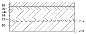
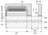
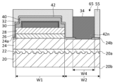
図1は、実施の形態に係る半導体発光素子10の構成を概略的に示す断面図である。半導体発光素子10は、基板20と、ベース層22と、n型半導体層24と、活性層26と、p型半導体層28と、p側コンタクト電極30と、p側電極被覆層32と、n側コンタクト電極34と、n側電極被覆層36と、p側パッド電極38pと、n側パッド電極38nと、第1保護層40と、第2保護層42と、第3保護層44とを備える。
FIG. 1 is a cross-sectional view schematically showing the configuration of a semiconductor
図1において、矢印Aで示される方向を「上下方向」または「厚み方向」ということがある。また、基板20から見て、基板20から離れる方向を上側、基板20に向かう方向を下側ということがある。
In FIG. 1, the direction indicated by arrow A may be referred to as the "vertical direction" or the "thickness direction." Also, when viewed from the
基板20は、半導体発光素子10が発する深紫外光に対して透光性を有する基板であり、例えば、サファイア(Al2O3)基板である。基板20は、第1主面20aと、第1主面20aとは反対側の第2主面20bとを有する。第1主面20aは、ベース層22からp型半導体層28までの各層を成長させるための結晶成長面となる一主面である。第1主面20aには、深さおよびピッチがサブミクロン(1μm以下)である微細な凹凸パターンが形成されている。このような基板20は、パターン化サファイア基板(PSS;Patterned Sapphire Substrate)とも呼ばれる。第2主面20bは、活性層26が発する深紫外光を外部に取り出すための光取り出し面となる一主面である。なお、基板20は、AlN基板であってもよいし、AlGaN基板であってもよい。基板20は、第1主面20aがパターン化されていない平坦面で構成される通常の基板であってもよい。
The
ベース層22は、基板20の第1主面20aの上に設けられる。ベース層22は、n型半導体層24を形成するための下地層(テンプレート層)である。ベース層22は、例えば、アンドープのAlN層であり、具体的には高温成長させたAlN(HT-AlN;High Temperature AlN)層である。ベース層22は、AlN層上に形成されるアンドープのAlGaN層を含んでもよい。基板20がAlN基板またはAlGaN基板である場合、ベース層22は、アンドープのAlGaN層のみで構成されてもよい。つまり、ベース層22は、アンドープのAlN層およびAlGaN層の少なくとも一方を含む。
The
n型半導体層24は、ベース層22の上に設けられる。n型半導体層24は、n型のAlGaN系半導体材料層であり、例えば、n型の不純物としてSiがドープされるAlGaN層である。n型半導体層24は、活性層26が発する深紫外光を透過するように組成比が選択され、例えば、AlNのモル分率が25%以上、好ましくは、40%以上または50%以上となるように形成される。n型半導体層24は、活性層26が発する深紫外光の波長よりも大きいバンドギャップを有し、例えば、バンドギャップが4.3eV以上となるように形成される。n型半導体層24は、AlNのモル分率が80%以下、つまり、バンドギャップが5.5eV以下となるように形成されることが好ましく、AlNのモル分率が70%以下(つまり、バンドギャップが5.2eV以下)となるように形成されることがより望ましい。n型半導体層24は、1μm~3μm程度の厚さを有し、例えば、2μm程度の厚さを有する。
The n-
n型半導体層24は、不純物であるSiの濃度が1×10¹⁸/cm3以上5×1019/cm3以下となるように形成される。n型半導体層24は、Si濃度が5×1018/cm3以上3×1019/cm3以下となるように形成されることが好ましく、7×1018/cm3以上2×1019/cm3以下となるように形成されることがより好ましい。ある実施例において、n型半導体層24のSi濃度は、1×1019/cm3前後であり、具体的には8×1018/cm3以上1.5×1019/cm3以下の範囲である。
The n-
n型半導体層24は、第1上面24aと、第2上面24bとを有する。第1上面24aは、活性層26が形成される部分である。第2上面24bは、活性層26が形成されずにn側コンタクト電極34および第2保護層42が形成される部分である。第1上面24aおよび第2上面24bは、互いに高さが異なり、基板20から第1上面24aまでの高さは、基板20から第2上面24bまでの高さよりも大きい。ここで、第1上面24aが位置する領域を「第1領域W1」と定義し、第2上面24bが位置する領域を「第2領域W2」と定義する。第2領域W2は、第1領域W1に隣接している。
The n-
活性層26は、n型半導体層24の第1上面24aの上に設けられる。活性層26は、AlGaN系半導体材料で構成され、n型半導体層24とp型半導体層28の間に挟まれてダブルへテロ接合構造を形成する。活性層26は、波長355nm以下の深紫外光を出力するためにバンドギャップが3.4eV以上となるように構成され、例えば、波長320nm以下の深紫外光を出力できるようにAlN組成比が選択される。
The
活性層26は、例えば、単層または多層の量子井戸構造を有し、アンドープのAlGaN系半導体材料で形成される障壁層と、アンドープのAlGaN系半導体材料で形成される井戸層との積層体で構成される。活性層26は、例えば、n型半導体層24と直接接触する第1障壁層と、第1障壁層の上に設けられる第1井戸層とを含む。第1障壁層と第1井戸層の間に、井戸層および障壁層の一以上のペアが追加的に設けられてもよい。障壁層および井戸層は、1nm~20nm程度の厚さを有し、例えば、2nm~10nm程度の厚さを有する。
The
活性層26は、p型半導体層28と直接接触する電子ブロック層をさらに含んでもよい。電子ブロック層は、アンドープのAlGaN系半導体材料層であり、例えば、AlNのモル分率が40%以上、好ましくは、50%以上となるように形成される。電子ブロック層は、AlNのモル分率が80%以上となるように形成されてもよく、GaNを含有しないAlN系半導体材料で形成されてもよい。電子ブロック層は、1nm~10nm程度の厚さを有し、例えば、2nm~5nm程度の厚さを有する。
p型半導体層28は、活性層26の上に形成される。p型半導体層28は、p型のAlGaN系半導体材料層またはp型のGaN系半導体材料層であり、例えば、p型の不純物としてマグネシウム(Mg)がドープされるAlGaN層またはGaN層である。p型半導体層28は、例えば、50nm~200nm程度の厚さを有する。
A p-
p型半導体層28は、複数層で構成されてもよい。p型半導体層28は、例えば、p型クラッド層とp型コンタクト層を有してもよい。p型クラッド層は、p型コンタクト層と比較してAlN比率の高いp型AlGaN層であり、活性層26と直接接触するように設けられる。p型コンタクト層は、p型クラッド層と比較してAlN比率の低いp型AlGaN層またはp型GaN層である。p型コンタクト層は、p型クラッド層の上に設けられ、p側コンタクト電極30と直接接触するように設けられる。
The p-
p型クラッド層は、活性層26が発する深紫外光を透過するように組成比が選択される。p型クラッド層は、例えば、AlNのモル分率が25%以上、好ましくは、40%以上または50%以上となるように形成される。p型クラッド層のAlN比率は、例えば、n型半導体層24のAlN比率と同程度、または、n型半導体層24のAlN比率よりも大きい。p型クラッド層のAlN比率は、70%以上または80%以上であってもよい。p型クラッド層は、20nm~100nm程度の厚さを有し、例えば、30nm~70nm程度の厚さを有する。
The composition ratio of the p-type cladding layer is selected so as to transmit the deep ultraviolet light emitted by the
p型クラッド層は、複数層で構成されてもよく、例えば、p型第1クラッド層とp型第2クラッド層を有してもよい。p型第1クラッド層は、p型第2クラッド層と比較してAlN比率の高いp型AlGaN層であり、活性層26と直接接触するように設けられる。p型第1クラッド層のAlN比率は、40%以上であり、好ましくは、50%以上または60%以上である。p型第2クラッド層は、p型第1クラッド層と比較してAlN比率の低いp型AlGaN層であり、p型第1クラッド層とp型コンタクト層の間に設けられる。p型第2クラッド層のAlN比率は、p型コンタクト層のAlN比率よりも高い。p型第2クラッド層のAlN比率は、25%以上であり、好ましくは、40%以上または50%以上である。p型第1クラッド層の厚さは、10nm~100nm程度であり、例えば15nm~70nm程度である。p型第2クラッド層の厚さは、5nm~25nm程度であり、例えば10nm~150nm程度である。
The p-type clad layer may be composed of multiple layers, and may have, for example, a p-type first clad layer and a p-type second clad layer. The p-type first clad layer is a p-type AlGaN layer having a higher AlN ratio than the p-type second clad layer, and is provided so as to be in direct contact with the
p型コンタクト層は、p側コンタクト電極30と良好なオーミック接触を得るためにAlN比率が20%以下となるよう構成され、好ましくは、AlN比率が10%以下、5%以下または0%となるように形成される。つまり、p型コンタクト層は、AlNを含有しないp型GaN系半導体材料で形成されてもよい。p型コンタクト層は、2nm~30nm程度の厚さを有し、例えば、10nm~20nm程度の厚さを有する。
The p-type contact layer is configured such that the AlN ratio is 20% or less in order to obtain good ohmic contact with the p-
p側コンタクト電極30は、p型半導体層28の上に設けられる。p側コンタクト電極30は、p型半導体層28(例えば、p型コンタクト層)とオーミック接触可能であり、活性層26が発する深紫外光に対する反射率が高い材料で構成される。このような特性の材料は限られているが、例えばロジウム(Rh)を用いることができる。p側コンタクト電極30をRh層とすることで、p型半導体層28とのコンタクト抵抗を1×10⁻²Ω・cm2以下(例えば1×10⁻⁴Ω・cm2以下)にすることができ、波長280nmの紫外光に対して60%以上(例えば60%~65%程度)の反射率を得ることができる。このとき、p側コンタクト電極30を構成するRh層の厚さは、50nm以上または100nm以上であることが好ましい。
A p-
p側コンタクト電極30は、第1領域W1の内側に形成される。ここで、p側コンタクト電極30が形成される領域を「第3領域W3」と定義する。p側コンタクト電極30は、第3領域W3の全体にわたってp型半導体層28とオーミック接触し、第3領域W3の全体にわたって深紫外光に対して高反射率となるように構成される。p側コンタクト電極30は、第3領域W3の全体にわたって厚さが均一となるように構成されることが好ましい。これにより、p側コンタクト電極30は、第3領域W3の全体において、活性層26からの紫外光を反射させて基板20の第2主面20bに向かわせる高効率の反射電極として機能するとともに、低抵抗のコンタクト電極として機能できる。
The p-
p側電極被覆層32は、p側コンタクト電極30を被覆するように設けられる。p側電極被覆層32は、p側コンタクト電極30の上面30aおよび側面30bの双方を被覆するように設けられる。p側電極被覆層32は、p側コンタクト電極30の外周においてp型半導体層28と接触するように設けられる。p側電極被覆層32は、p側コンタクト電極30と第1保護層40の界面の全体にわたって形成され、p側コンタクト電極30と第1保護層40が直接接触しないように形成される。p側電極被覆層32は、チタン(Ti)または導電性を有する窒化チタン(TiN)で構成される。導電性を有するTiNの導電率は、1×10⁻⁵Ω・m以下であり、例えば4×10⁻⁷Ω・m程度である。p側電極被覆層32の厚みは、5nm以上であり、例えば10nm~100nm程度である。
The p-side
n側コンタクト電極34は、n型半導体層24の第2上面24bの上に設けられる。n側コンタクト電極34は、活性層26が設けられる第1領域W1とは異なる第2領域W2に設けられる。n側コンタクト電極34は、第2領域W2の内側に形成される。n側コンタクト電極34は、第2保護層42の上に重なるように設けられ、第2保護層42を貫通するn側コンタクト開口42nにおいてn型半導体層24の第2上面24bと接触する。ここで、n側コンタクト電極34が形成される領域を「第4領域W4」と定義し、n側コンタクト電極34がn型半導体層24と接触する領域を「第5領域W5」と定義する。第4領域W4は、第5領域W5よりも大きく、第4領域W4の内側に第5領域W5の全体が収まっている。
The n-
n側コンタクト電極34は、n型半導体層24とオーミック接触が可能であり、かつ、活性層26が発する深紫外光に対する反射率が高い材料で構成される。n側コンタクト電極34は、n型半導体層24に直接接触するTi層と、Ti層に直接接触するアルミニウム(Al)層とを含む。Ti層の厚さは1nm~10nm程度であり、5nm以下であることが好ましく、1nm~2nmであることがより好ましい。Ti層の厚さを小さくすることで、n型半導体層24から見たときのn側コンタクト電極34の紫外光反射率を高めることができる。Al層の厚さは100nm~1000nm程度であり、200nm以上であることが好ましい。Al層の厚さを大きくすることで、n側コンタクト電極34の紫外光反射率を高めることができる。
The n-
n側コンタクト電極34は、例えば、第5領域W5の全体にわたってn型半導体層24とオーミック接触する。n側コンタクト電極34としてTi/Al層を用いることで、1×10-2Ω・cm2以下(例えば1×10-3Ω・cm2以下)のコンタクト抵抗を実現できる。n側コンタクト電極34は、第4領域W4の全体にわたって深紫外光に対して高反射率となるように構成される。n側コンタクト電極34は、Tiの厚みを小さくすることにより、波長280nmの紫外光に対して80%以上(例えば85%~90%程度)の反射率を得ることができる。
The n-
n側コンタクト電極34は、第5領域W5の全体にわたって均一に構成されることが好ましい。言いかえれば、n側コンタクト電極34を構成するTi層およびAl層は、第5領域W5の全体にわたって均一の厚みで積層されることが好ましい。これにより、n側コンタクト電極34は、n型半導体層24と接触する第5領域W5の全体において、活性層26からの紫外光を反射させて基板20の第2主面20bに向かわせる高効率の反射電極として機能するとともに、低抵抗のコンタクト電極として機能できる。なお、n側コンタクト電極34は、紫外光反射率の低下の要因となりうる金(Au)を含有しないことが好ましい。
The n-
n側電極被覆層36は、n側コンタクト電極34を被覆するように設けられる。n側電極被覆層36は、n側コンタクト電極34の上面34aおよび側面34bの双方を被覆するように設けられる。n側電極被覆層36は、n側コンタクト電極34の外周において第2保護層42と接触するように設けられる。n側電極被覆層36は、n側コンタクト電極34と第3保護層44の界面の全体にわたって形成され、n側コンタクト電極34と第3保護層44が直接接触しないように形成される。n側電極被覆層36は、p側電極被覆層32と同様、Tiまたは導電性を有するTiNで構成される。n側電極被覆層36の厚みは、5nm以上であり、例えば10nm~100nm程度である。
The n-side
p側パッド電極38pおよびn側パッド電極38n(総称してパッド電極ともいう)は、半導体発光素子10をパッケージ基板などに実装する際にボンディング接合される部分である。p側パッド電極38pは、p側コンタクト電極30の上に設けられる。p側パッド電極38pは、第1保護層40、第2保護層42および第3保護層44を貫通するp側パッド開口48においてp側電極被覆層32と接触し、p側コンタクト電極30と電気的に接続される。n側パッド電極38nは、n側コンタクト電極34の上に設けられる。n側パッド電極38nは、第3保護層44を貫通するn側パッド開口44nにおいてn側電極被覆層36と接触し、n側コンタクト電極34と電気的に接続される。パッド電極38p,38nは、第3保護層44の上に重なるように設けられる。
The p-
パッド電極38p,38nは、耐腐食性の観点からAuを含有するように構成され、例えば、Ni/Au、Ti/AuまたはTi/Pt/Auの積層構造で構成される。パッド電極38p,38nが金錫(AuSn)で接合される場合、金属接合材となるAuSn層をパッド電極38p,38nが含んでもよい。
The
第1保護層40は、p側電極被覆層32を被覆する。第1保護層40は、p側電極被覆層32の上面の一部に設けられる第1p側パッド開口40pを有し、第1p側パッド開口40pとは異なる箇所においてp側電極被覆層32の上面および側面を被覆する。第1保護層40はさらに、p型半導体層28の上面28aを被覆する。第1保護層40は、p型半導体層28の上面28aのうちp側コンタクト電極30が形成される第3領域W3とは異なる領域、つまり、第3領域W3を除く第1領域W1の全体を被覆する。したがって、第1保護層40は、第1p側パッド開口40pを除いて、p側電極被覆層32の露出面の全体と、p型半導体層28の上面28aの露出部分の全体とを被覆する。第1保護層40は、酸化シリコン(SiO2)または酸窒化シリコン(SiON)で構成される。第1保護層40の厚みは、50nm以上であり、例えば100nm以上500nm以下である。
The first
第1保護層40は、p型半導体層28に比べて活性層26から出力される深紫外光に対する屈折率が低い材料で構成される。p型半導体層28を構成するAlGaN系半導体材料の屈折率は組成比によるが2.1~2.56程度である。一方、第1保護層40を構成するSiO2の屈折率は1.4程度であり、SiONの屈折率は1.4~2.1程度である。低屈折率の第1保護層40を設けることで、p型半導体層28と第1保護層40の界面で活性層26からの紫外光のより多くを全反射させ、光取出面である基板20の第2主面20bに向かわせることができる。特に、酸化シリコン(SiO2)はp型半導体層28との屈折率差が大きいため、反射特性をより高めることができる。
The first
第1p側パッド開口40pは、p側パッド電極38pを設けるために形成される。第1p側パッド開口40pは、p側コンタクト電極30の上に設けられ、第1保護層40を貫通してp側電極被覆層32を露出させる。第1p側パッド開口40pの開口領域は、p側コンタクト電極30が形成される第3領域W3よりも小さく、第3領域W3の内側に収まっている。
The first p-
第2保護層42は、第1保護層40を被覆する。第2保護層42は、第1p側パッド開口40pと連通する第2p側パッド開口42pを有し、第2p側パッド開口42pとは異なる箇所において第1保護層40の露出面を被覆する。第2保護層42は、n型半導体層24、活性層26およびp型半導体層28の側面(メサ面46ともいう)を被覆する。第2保護層42はさらに、n型半導体層24の第2上面24bの一部に設けられるn側コンタクト開口42nを有し、n側コンタクト開口42nとは異なる箇所にてn型半導体層24の第2上面24bを被覆する。第2保護層42は、第1領域W1および第2領域W2の双方にわたって設けられる。したがって、第2保護層42は、第2p側パッド開口42pおよびn側コンタクト開口42nを除いて、第1保護層40の露出面、p型半導体層28の側面、活性層26の側面およびn型半導体層24の第2上面24bの露出部分の全体を被覆する。第2保護層42の一部は、第5領域W5を除く第4領域W4において、n型半導体層24の第2上面24bとn側コンタクト電極34の間に挟み込まれている。
A second
第2保護層42は、酸化アルミニウム(Al2O3)で構成される。第2保護層42の厚みは、10nm以上50nm以下とすることができ、例えば、20nm~30nm程度とすることができる。半導体層の上面および側面の実質的に全体をAl2O3の第2保護層42で被覆することで、耐湿性に優れた保護機能を提供できる。図1では、メサ面46が基板20に対して垂直となるように示されているが、メサ面46は基板20に対して所定の傾斜角で傾斜していてもよい。メサ面46の傾斜角は、例えば、40度以上55度未満であってもよい。
The second
第2保護層42は、膜密度の高い緻密な構造であることが好ましく、例えば原子層堆積(ALD;Atomic Layer Deposition)法を用いて形成されることが好ましい。また、第2保護層42は、水素濃度が低いことが好ましい。第2保護層42に高濃度の水素(H)が含まれていると、活性層26やp型半導体層28に水素が拡散し、これらの半導体層を劣化させる原因となる。水素濃度の低いAl2O3とするため、酸素原子の供給源として、水(H2O)ではなく、酸素ガス(O2)プラズマやオゾンガス(O3)を用いることが好ましい。つまり、第2保護層42は、トリメチルアルミニウム(TMA)などの有機アルミニウム化合物と、O2プラズマまたはO3とを原料とするALD法により形成されることが好ましい。
The second
n側コンタクト開口42nは、n側コンタクト電極34を設けるために形成される。n側コンタクト開口42nは、n型半導体層24の第2上面24bの上に設けられ、第2保護層42を貫通してn型半導体層24を露出させる。n側コンタクト開口42nの開口領域(第5領域W5)は、n側コンタクト電極34が形成される第4領域W4よりも小さい。したがって、n側コンタクト開口42nの外縁において、第2保護層42の上にn側コンタクト電極34が重なっている。
The n-
第2p側パッド開口42pは、p側パッド電極38pを設けるために形成される。第2p側パッド開口42pは、p側コンタクト電極30の上に設けられ、第2保護層42を貫通する。第2p側パッド開口42pは、第1p側パッド開口40pと連通してp側電極被覆層32を露出させる。第2p側パッド開口42pの開口領域は、例えば、p側コンタクト電極30が形成される第3領域W3よりも小さく、第1p側パッド開口40pの開口領域よりも大きい。第1p側パッド開口40pの開口領域は、第2p側パッド開口42pの開口領域の内側に収まっている。
A second p-
第3保護層44は、第2保護層42の大部分およびn側電極被覆層36を被覆する。第3保護層44は、p側コンタクト電極30の上に設けられる第3p側パッド開口44pを有し、第3p側パッド開口44pとは異なる箇所において第2保護層42の露出面を被覆する。第3保護層44はさらに、n側コンタクト電極34の上に設けられるn側パッド開口44nを有し、n側パッド開口44nとは異なる箇所においてn側電極被覆層36の露出面を被覆する。したがって、第3保護層44は、n側電極被覆層36の上面および側面を被覆し、n側コンタクト電極34を被覆するように設けられる。第3保護層44は、第1領域W1および第2領域W2の双方にわたって設けられる。第3保護層44は、第3p側パッド開口44pおよびn側パッド開口44nを除いて、第2保護層42の露出面の大部分およびn側電極被覆層36の露出面の全体を被覆する。
The third
第3保護層44は、SiO2またはSiONで構成される。第3保護層44の厚さは、200nm以上であり、例えば500nm~1000nm程度である。第3保護層44の厚さを大きくすることで、半導体層に比べて厚みの大きいn側コンタクト電極34を好適に被覆できる。
The third
第3p側パッド開口44pは、p側パッド電極38pを設けるために形成される。第3p側パッド開口44pは、p側コンタクト電極30の上に設けられ、第3保護層44を貫通する。第3p側パッド開口44pは、第1p側パッド開口40pおよび第2p側パッド開口42pと連通してp側電極被覆層32を露出させる。図示する例では、第3p側パッド開口44pの開口領域は、第1p側パッド開口40pや第2p側パッド開口42pの開口領域よりも大きい。第1p側パッド開口40pや第2p側パッド開口42pは、第3p側パッド開口44pの内側に収まっている。なお、第3p側パッド開口44pの開口領域は、第1p側パッド開口40pや第2p側パッド開口42pの開口領域より小さくてもよい。
A third p-
n側パッド開口44nは、n側パッド電極38nを設けるために形成される。n側パッド開口44nは、n側コンタクト電極34の上に設けられ、第3保護層44を貫通してn側電極被覆層36を露出させる。n側パッド開口44nの開口領域は、n側コンタクト電極34が設けられる第4領域W4よりも小さい。n側パッド開口44nの開口領域は、n側コンタクト開口42nの開口領域(第5領域W5)よりも小さくてもよいし、大きくてもよい。
The n-
つづいて、半導体発光素子10の製造方法について説明する。図2~図14は、半導体発光素子10の製造工程を概略的に示す図である。図2において、まず、基板20の第1主面20aの上にベース層22、n型半導体層24、活性層26、p型半導体層28を順に形成する。活性層26は、n型半導体層24の第1上面24aに形成される。
Next, a method for manufacturing the semiconductor
基板20は、パターン化サファイア基板であり、AlGaN系半導体材料を形成するための成長基板である。ベース層22は、例えば、高温成長させたAlN(HT-AlN)層と、アンドープのAlGaN(u-AlGaN)層とを含む。n型半導体層24、活性層26およびp型半導体層28は、AlGaN系半導体材料、AlN系半導体材料またはGaN系半導体材料で形成される層であり、有機金属化学気相成長(MOVPE;Metal Organic Vapor Phase Epitaxy)法や、分子線エピタキシ(MBE;Molecular Beam Epitaxy)法などの周知のエピタキシャル成長法を用いて形成できる。
The
次に、図3に示すように、p型半導体層28の上に第1マスク51を形成し、第1マスク51が設けられていない第1開口61においてp側コンタクト電極30を形成する。第1マスク51は、例えば、公知のフォトリソグラフィ技術を用いて形成できる。第1マスク51の第1開口61は、p側コンタクト電極30を形成すべき第3領域W3に位置する。p側コンタクト電極30は、スパッタリング法や電子ビーム(EB;Electron Beam)蒸着法で形成することができる。p側コンタクト電極30は、p型半導体層28の上面28aと直接接触する。p側コンタクト電極30を形成して第1マスク51を除去した後、p側コンタクト電極30にアニール処理が施される。
Next, as shown in FIG. 3, a
次に、図4に示すように、p型半導体層28の上に第2マスク52を形成し、第2マスク52が設けられていない第2開口62においてp側電極被覆層32を形成する。第2マスク52は、例えば、公知のフォトリソグラフィ技術を用いて形成できる。第2マスク52の第2開口62は、第3領域W3よりも少しだけ大きい範囲に形成され、第2開口62の内側にp側コンタクト電極30が収まるように形成される。p側電極被覆層32は、p側コンタクト電極30の上面30aおよび側面30bを被覆し、p型半導体層28の上面28aに接触するように形成される。p側電極被覆層32は、例えば、反応性スパッタリング法により形成できる。p側電極被覆層32の形成後、第2マスク52が除去される。
Next, as shown in FIG. 4, a
次に、図5に示すように、p型半導体層28の上面28aを被覆するとともに、p側電極被覆層32の上面および側面を被覆するように第1保護層40が形成される。第1保護層40は、化学気相成長(CVD)法などの周知の技術を用いて形成できる。
Next, as shown in FIG. 5 , a first
次に、図6に示すように、第1保護層40の上に第3マスク53を形成し、第3マスク53が設けられていない第3開口63に位置する第1保護層40、p型半導体層28および活性層26をドライエッチングにより除去する。第3マスク53は、例えば、公知のフォトリソグラフィ技術を用いて形成できる。第3マスク53は、第1領域W1のみに形成され、第3開口63が第2領域W2に位置する。ドライエッチングは、第2領域W2においてn型半導体層24の第2上面24bが露出するまで実行される。この工程により、第1領域W1にメサ面46を有する活性層26およびp型半導体層28が形成される。メサ面46を形成する工程では、塩素系のエッチングガスを用いた反応性イオンエッチングを用いることができ、誘導結合型プラズマ(ICP;Inductively Coupled Plasma)エッチングを用いることができる。例えば、エッチングガスとして塩素(Cl2)、三塩化ホウ素(BCl3)、四塩化ケイ素(SiCl4)などの塩素(Cl)を含む反応性ガスを用いることができる。なお、反応性ガスと不活性ガスを組み合わせてドライエッチングしてもよく、塩素系ガスにアルゴン(Ar)などの希ガスを混合させてもよい。メサ面46の形成後、第3マスク53が除去される。
Next, as shown in FIG. 6, a
次に、図7に示すように、第1領域W1および第2領域W2の双方にわたって第2保護層42が形成される。第2保護層42は、第1保護層40を被覆し、p型半導体層28の側面、活性層26の側面およびn型半導体層24の側面(メサ面46)を被覆し、n型半導体層24の露出した第2上面24bを被覆する。第1保護層40は、例えばTMAと、O2プラズマまたはO3とを原料とするALD法により形成される。
Next, as shown in FIG. 7, a second
次に、図8に示すように、第2保護層42の上に第4マスク54を形成し、第4マスク54が設けられていない第4開口64に位置する第2保護層42をドライエッチングにより除去する。第4開口64は、n側コンタクト開口42nが形成されるべき第5領域W5に位置する。第2保護層42は、塩素系ガス、または、塩素系ガスと希ガスの混合ガスを用いてドライエッチングすることができる。これにより、第2保護層42を貫通するn側コンタクト開口42nが形成され、n側コンタクト開口42nにおいてn型半導体層24が露出する。n側コンタクト開口42nは、n型半導体層24の第2上面24bの一部に設けられる。n側コンタクト開口42nの形成後、第4マスク54が除去される。
Next, as shown in FIG. 8, a
次に、図9に示すように、第2保護層42の上に第5マスク55を形成し、第5マスク55が設けられていない第5開口65においてn側コンタクト電極34を形成する。第5マスク55は、例えば、公知のフォトリソグラフィ技術を用いて形成できる。第5開口65は、n側コンタクト電極34が形成されるべき第4領域W4に位置する。第5開口65は、n側コンタクト開口42nの開口領域よりも広い。第5開口65において、まずTi層が形成される。Ti層は、n側コンタクト開口42nにおいてn型半導体層24と直接接触し、n側コンタクト開口42nの外縁において第2保護層42の上に重なるように設けられる。次にTi層の上にAl層が形成される。Ti層およびAl層は、スパッタリング法やEB蒸着法で形成される。
Next, as shown in FIG. 9, a
つづいて、第5マスク55を除去し、n側コンタクト電極34にアニール処理を施す。n側コンタクト電極34のアニール処理は、Alの融点(約660℃)未満の温度で実行され、例えば550℃以上650℃以下、好ましくは560℃以上610℃以下の温度でアニールされる。n側コンタクト電極34のAl層の膜密度を2.6g/cm3以上2.7g/cm3未満とすることで、n側コンタクト電極34のコンタクト抵抗を1×10-2Ω・cm2以下にできる。また、アニール温度をAlの融点未満とすることで、アニール後のn側コンタクト電極34の平坦性を高め、紫外光反射率を80%以上にすることができる。
Subsequently, the
次に、図10に示すように、第2保護層42の上に第6マスク56を形成し、第6マスク56が設けられていない第6開口66においてn側電極被覆層36を形成する。第6マスク56は、例えば、公知のフォトリソグラフィ技術を用いて形成できる。第6マスク56の第6開口66は、第4領域W4よりも少しだけ大きい範囲に形成され、第6開口66の内側にn側コンタクト電極34が収まるように形成される。n側電極被覆層36は、n側コンタクト電極34の上面34aおよび側面34bを被覆し、第2保護層42に接触するように形成される。n側電極被覆層36は、例えば、反応性スパッタリング法により形成できる。n側電極被覆層36の形成後、第6マスク56が除去される。
Next, as shown in FIG. 10, a
次に、図11に示すように、第2保護層42およびn側電極被覆層36の上に第7マスク57を形成し、第7マスク57が設けられていない第7開口67において第2保護層42を除去する。第7マスク57は、例えば、公知のフォトリソグラフィ技術を用いて形成できる。第7開口67は、p側コンタクト電極30と重なる位置に設けられ、p側コンタクト電極30が設けられる第3領域W3よりも狭い範囲に設けられる。第2保護層42は、塩素系ガス、または、塩素系ガスと希ガスの混合ガスを用いてドライエッチングすることができる。これにより、第2保護層42を貫通する第2p側パッド開口42pが形成され、第2p側パッド開口42pにおいて第1保護層40が露出する。このドライエッチング工程において、第1保護層40の露出部分が所定の深さだけ除去されてもよい。第2p側パッド開口42pの形成後、第7マスク57が除去される。
Next, as shown in FIG. 11, a
次に、図12に示すように、第1保護層40、第2保護層42およびn側電極被覆層36の上に第8マスク58を形成し、第8マスク58が設けられていない第8開口68において第1保護層40を除去する。第8マスク58は、例えば、公知のフォトリソグラフィ技術を用いて形成できる。第8開口68は、p側コンタクト電極30と重なる位置に設けられ、第2p側パッド開口42pよりも狭い範囲に設けられる。第8マスク58は、第2保護層42の露出面を完全に被覆するように設けられ、第2p側パッド開口42pにおける第2保護層42の側壁を被覆して保護するように設けられる。第1保護層40は、CF系のエッチングガスを用いてドライエッチングすることができ、例えば、六フッ化エタン(C2F6)を用いることができる。これにより、第1保護層40を貫通する第1p側パッド開口40pが形成され、第1p側パッド開口40pにおいてp側電極被覆層32が露出する。このドライエッチング工程において、p側電極被覆層32がエッチングストップ層として機能し、p側電極被覆層32の下のp側コンタクト電極30へのダメージを防ぐことができる。第1p側パッド開口40pの形成後、第8マスク58が除去される。
Next, as shown in FIG. 12, an
次に、図13に示すように、第2保護層42およびn側電極被覆層36を被覆するように第3保護層44を形成する。第3保護層44は、第1領域W1および第2領域W2の双方にわたって形成され、素子構造の上面の全体を被覆するように形成される。第3保護層44は、第1p側パッド開口40pおよび第2p側パッド開口42pにおいて露出するp側電極被覆層32を被覆するように形成される。したがって、第1p側パッド開口40pおよび第2p側パッド開口42pは、第3保護層44によって塞がれる。第3保護層44は、化学気相成長(CVD)法などの周知の技術を用いて形成できる。
Next, as shown in FIG. 13, a third
次に、図14に示すように、第3保護層44の上に第9マスク59を形成し、第9マスク59が設けられていない第9開口69p,69nにおいて第3保護層44を除去する。第9マスク59は、例えば、公知のフォトリソグラフィ技術を用いて形成できる。第9開口69p,69nは、それぞれp側コンタクト電極30およびn側コンタクト電極34の上に位置する。第3保護層44は、CF系のエッチングガスを用いてドライエッチングすることができ、例えば、六フッ化エタン(C2F6)を用いることができる。p側第9開口69pでは、第1保護層40および第2保護層42が除去された箇所の第3保護層44が除去され、第3保護層44を貫通する第3p側パッド開口44pが形成される。第3p側パッド開口44pは、第2p側パッド開口42pおよび第1p側パッド開口40pと連通し、p側電極被覆層32を露出させるp側パッド開口48を構成する。n側第9開口69nでは、第3保護層44が除去され、第3保護層44を貫通するn側パッド開口44nが形成される。
Next, as shown in FIG. 14, a
図14に示すドライエッチング工程では、図12に示すドライエッチング工程と同様、p側電極被覆層32およびn側電極被覆層36がエッチングストップ層として機能する。そのため、p側コンタクト電極30およびn側コンタクト電極34へのダメージを防ぐことができ、低抵抗かつ高反射率のコンタクト電極を維持できる。特に、p側電極被覆層32およびn側電極被覆層36がTiNで構成される場合、TiNがフッ素系のエッチングガスとの反応性が低いため、エッチングによる副生成物も発生しにくい。その結果、ドライエッチングの実行後であっても、p側電極被覆層32およびn側電極被覆層36の露出面を高品質に維持できる。
In the dry etching process shown in FIG. 14, the p-side
図14に示すドライエッチング工程では、実質的に第3保護層44のみが除去されるため、n側パッド開口44nを形成するためのエッチング深さと、第3p側パッド開口44pを形成するためのエッチング深さとを同等にできる。これは、図13の工程において第3保護層44を形成する前に、p側コンタクト電極30の上を被覆する第1保護層40および第2保護層42を図11および図12の工程にて除去することで実現される。事前にp側コンタクト電極30の上の第1保護層40および第2保護層42を除去していない場合、図14に示すドライエッチング工程において、p側コンタクト電極30の上の第1保護層40、第2保護層42および第3保護層44を連続的に除去する必要が生じる。つまり、p側コンタクト電極30およびn側コンタクト電極34の上の第3保護層44を除去した後、p側コンタクト電極30の上の第1保護層40および第2保護層42を除去しなければならない。そうすると、n側電極被覆層36が露出した状態でドライエッチング工程を継続する必要が生じ、n側電極被覆層36にダメージが生じるおそれがある。一方、本実施の形態では、図14に示すドライエッチング工程において、第3保護層44を除去してp側電極被覆層32およびn側電極被覆層36を露出させるタイミングをほぼ同時にできるため、n側電極被覆層36のオーバーエッチングを防止できる。
In the dry etching step shown in FIG. 14, only the third
つづいて、p側パッド開口48においてp側電極被覆層32の上にp側パッド電極38pを形成し、n側パッド開口44nにおいてn側電極被覆層36の上にn側パッド電極38nを形成する。パッド電極38n,38pは、例えば、Ni層またはTi層をp側電極被覆層32およびn側コンタクト電極34の上に堆積し、その上にAu層を堆積することで形成できる。Au層の上にさらに別の金属層が設けられてもよく、例えば、Sn層、AuSn層、Sn/Auの積層構造を形成してもよい。パッド電極38n,38pは、第9マスク59を利用して形成されてもよいし、第9マスク59とは別のレジストマスクを利用して形成されてもよい。パッド電極38n,38pの形成後、第9マスク59または別のレジストマスクが除去される。以上の工程により、図1に示す半導体発光素子10ができあがる。
Subsequently, a p-
本実施の形態によれば、p側コンタクト電極30と第1保護層40の間にTiまたはTiNで構成されるp側電極被覆層32が設けられるため、p側コンタクト電極30に対する第1保護層40の密着性を高めることができる。特に、p側コンタクト電極30を構成するRhは、シリコンまたはアルミニウムの酸化物、酸窒化物、窒化物といった誘電体材料との密着性が低い。そのため、p側コンタクト電極30に第1保護層40が直接接触する構造の場合、p側コンタクト電極30から第1保護層40が剥離しやすく、第1保護層40、第2保護層42および第3保護層44による絶縁性や耐湿性といった封止機能が低下してしまう。一方、本実施の形態によれば、p側電極被覆層32を設けることで、p側コンタクト電極30からの第1保護層40の剥離を防止でき、保護層40,42,44による封止機能の低下を防ぐことができる。これにより、半導体発光素子10の信頼性を高めることができる。
According to the present embodiment, since the p-side
図15は、別の実施の形態に係る半導体発光素子110の構成を概略的に示す断面図である。本実施の形態では、p側パッド開口148が第3保護層144の側壁のみで構成される点で上述の実施の形態と相違する。第3保護層144は、第1保護層40の第1p側パッド開口40pの側壁と、第2保護層42の第2p側パッド開口42pの側壁とを被覆するように設けられる。したがって、p側パッド開口148を形成する第3保護層144の開口領域は、第1p側パッド開口40pおよび第2p側パッド開口42pのそれぞれの開口領域よりも小さい。
FIG. 15 is a cross-sectional view schematically showing the configuration of a semiconductor
図16は、図15の半導体発光素子110の製造工程を概略的に示す図である。図16は、上述の実施の形態の図14の工程に対応する。図16に示されるように、第9マスク159が設けられていないp側第9開口169pの開口領域は、第1p側パッド開口40pおよび第2p側パッド開口42pの開口領域よりも狭い。p側第9開口169pにおいて第3保護層144をドライエッチングすることにより、第3保護層144を貫通するp側パッド開口148が形成され、p側パッド開口148においてp側電極被覆層32が露出する。その後、パッド電極38p,38nを形成することで、図15に示す半導体発光素子110ができあがる。
16A and 16B schematically show the manufacturing process of the semiconductor
本実施の形態においても、上述の実施の形態と同様の効果を奏することができる。 Also in this embodiment, the same effects as those of the above-described embodiments can be obtained.
以上、本発明を実施例にもとづいて説明した。本発明は上述の実施の形態に限定されず、種々の設計変更が可能であり、様々な変形例が可能であること、またそうした変形例も本発明の範囲にあることは、当業者に理解されるところである。 The present invention has been described above based on the examples. Those skilled in the art will understand that the present invention is not limited to the above-described embodiments, and that various design changes and modifications are possible, and that such modifications are within the scope of the present invention. It is about to be done.
10…半導体発光素子、24…n型半導体層、26…活性層、28…p型半導体層、28a…上面、30…p側コンタクト電極、32…p側電極被覆層、34…n側コンタクト電極、36…n側電極被覆層、38n…n側パッド電極、38p…p側パッド電極、40…第1保護層、42…第2保護層、42n…n側コンタクト開口、44…第3保護層、44n…n側パッド開口、46…メサ面、48…p側パッド開口。
DESCRIPTION OF
Claims (9)
前記n型半導体層の第1上面に設けられ、AlGaN系半導体材料から構成される活性層と、
前記n型半導体層の第2上面と接触して設けられるn側コンタクト電極と、
前記活性層上に設けられるp型半導体層と、
前記p型半導体層の上面と接触し、Rhから構成されるp側コンタクト電極と、
前記p側コンタクト電極の上面および側面を被覆し、TiNから構成されるp側電極被覆層と、
前記p側電極被覆層の上面の一部に設けられる第1p側パッド開口を有し、前記第1p側パッド開口とは異なる箇所において前記p側電極被覆層の上面および側面を被覆し、SiO2またはSiONから構成される第1保護層と、
前記第1p側パッド開口と連通する第2p側パッド開口を有し、前記第2p側パッド開口とは異なる箇所において前記第1保護層、前記p型半導体層の側面および前記活性層の側面を被覆し、Al2O3から構成される第2保護層と、
前記第1p側パッド開口および前記第2p側パッド開口において前記p側電極被覆層と接触するp側パッド電極と、を備えることを特徴とする半導体発光素子。 an n-type semiconductor layer made of an n-type AlGaN semiconductor material;
an active layer provided on the first upper surface of the n-type semiconductor layer and made of an AlGaN-based semiconductor material;
an n-side contact electrode provided in contact with the second upper surface of the n-type semiconductor layer;
a p-type semiconductor layer provided on the active layer;
a p-side contact electrode made of Rh in contact with the upper surface of the p-type semiconductor layer;
a p-side electrode covering layer made of TiN covering the upper and side surfaces of the p-side contact electrode;
a first p-side pad opening provided in a part of the upper surface of the p-side electrode covering layer, covering the upper surface and side surfaces of the p-side electrode covering layer at a location different from the first p-side pad opening, and comprising SiO 2 or a first protective layer made of SiON;
a second p-side pad opening communicating with the first p-side pad opening, covering the first protective layer, the side surface of the p-type semiconductor layer, and the side surface of the active layer at locations different from the second p-side pad opening; and a second protective layer made of Al 2 O 3 ;
a p-side pad electrode in contact with the p-side electrode covering layer in the first p-side pad opening and the second p-side pad opening.
前記n側コンタクト電極は、前記n側コンタクト開口において前記n型半導体層の前記第2上面と接触し、前記n側コンタクト開口の外縁において前記第2保護層の上に重なることを特徴とする請求項1に記載の半導体発光素子。 The second protective layer has an n-side contact opening provided in a part of the second upper surface of the n-type semiconductor layer, and the second protective layer of the n-type semiconductor layer at a location different from the n-side contact opening. 2 further coat the top surface,
The n-side contact electrode is in contact with the second upper surface of the n-type semiconductor layer at the n-side contact opening and overlaps the second protective layer at the outer edge of the n-side contact opening. Item 1. The semiconductor light emitting device according to item 1.
前記第1保護層は、前記p側コンタクト電極および前記p側電極被覆層が設けられる箇所とは異なる箇所において前記p型半導体層の前記上面をさらに被覆することを特徴とする請求項1または2に記載の半導体発光素子。 The p-side electrode covering layer is provided so as to be in contact with the p-type semiconductor layer,
3. The first protective layer further covers the upper surface of the p-type semiconductor layer at a location different from a location where the p-side contact electrode and the p-side electrode covering layer are provided. 3. The semiconductor light emitting device according to .
前記n側パッド開口に設けられるn側パッド電極と、をさらに備え、
前記p側パッド電極および前記n側パッド電極は、前記第3保護層の上に重なることを特徴とする請求項1から3のいずれか一項に記載の半導体発光素子。 a third p-side pad opening provided on the p-side contact electrode and an n-side pad opening provided on the n-side contact electrode, and covering the second protective layer at a location different from the third p-side pad opening; a third protective layer made of SiO 2 covering the n-side contact electrode at a location different from the n-side pad opening;
an n-side pad electrode provided in the n-side pad opening ,
4. The semiconductor light emitting device according to claim 1 , wherein said p-side pad electrode and said n-side pad electrode overlap said third protective layer .
前記第3保護層は、前記n側パッド開口とは異なる箇所において前記n側電極被覆層を被覆し、
前記n側パッド電極は、前記n側パッド開口において前記n側電極被覆層と接触することを特徴とする請求項4に記載の半導体発光素子。 further comprising an n-side electrode covering layer made of TiN that covers the top and side surfaces of the n-side contact electrode and is in contact with the second protective layer;
the third protective layer covers the n-side electrode covering layer at a location different from the n-side pad opening;
5. The semiconductor light emitting device according to claim 4, wherein said n-side pad electrode is in contact with said n-side electrode cover layer at said n-side pad opening.
前記活性層上にp型半導体層を形成する工程と、
前記p型半導体層の上面と接触し、Rhから構成されるp側コンタクト電極を形成する工程と、
前記p側コンタクト電極を被覆し、TiNから構成されるp側電極被覆層を形成する工程と、
前記p型半導体層の上面を被覆するとともに、前記p側電極被覆層の上面および側面を被覆し、SiO2またはSiONから構成される第1保護層を形成する工程と、
前記p側コンタクト電極が形成された領域とは異なる領域において前記第1保護層、前記p型半導体層および前記活性層を除去し、前記n型半導体層の第2上面を露出させる工程と、
前記第1保護層、前記p型半導体層の側面および前記活性層の側面を被覆し、Al2O3から構成される第2保護層を形成する工程と、
前記n型半導体層の前記第2上面と接触するn側コンタクト電極を形成する工程と、
前記p側コンタクト電極上の前記第2保護層を貫通する第2p側パッド開口を形成する工程と、
前記p側コンタクト電極上の前記第1保護層を貫通し、前記第2p側パッド開口と連通する第1p側パッド開口を形成する工程と、
前記第1p側パッド開口にて露出する前記p側電極被覆層に接触するp側パッド電極を形成する工程と、を備えることを特徴とする半導体発光素子の製造方法。 forming an active layer made of an AlGaN-based semiconductor material on a first upper surface of an n-type semiconductor layer made of an n-type AlGaN-based semiconductor material;
forming a p-type semiconductor layer on the active layer;
forming a p-side contact electrode made of Rh in contact with the upper surface of the p-type semiconductor layer;
a step of covering the p-side contact electrode and forming a p-side electrode covering layer made of TiN;
forming a first protective layer composed of SiO 2 or SiON covering the upper surface of the p-type semiconductor layer and covering the upper surface and side surfaces of the p-side electrode covering layer;
removing the first protective layer, the p-type semiconductor layer and the active layer in a region different from the region where the p-side contact electrode is formed to expose a second upper surface of the n-type semiconductor layer;
forming a second protective layer made of Al 2 O 3 covering the side surfaces of the first protective layer, the p-type semiconductor layer, and the active layer;
forming an n-side contact electrode in contact with the second upper surface of the n-type semiconductor layer;
forming a second p-side pad opening penetrating the second protective layer on the p-side contact electrode;
forming a first p-side pad opening penetrating the first protective layer on the p-side contact electrode and communicating with the second p-side pad opening;
forming a p-side pad electrode in contact with the p-side electrode covering layer exposed in the first p-side pad opening.
前記n型半導体層の前記第2上面の一部に設けられる前記第2保護層を貫通するn側コンタクト開口を形成する工程をさらに備え、
前記n側コンタクト電極は、前記n側コンタクト開口の外縁において前記第2保護層の上に重なるように形成されることを特徴とする請求項7に記載の半導体発光素子の製造方法。 the second protective layer is formed to further cover the second upper surface of the n-type semiconductor layer;
forming an n-side contact opening penetrating the second protective layer provided on a portion of the second upper surface of the n-type semiconductor layer;
8. The method of manufacturing a semiconductor light emitting device according to claim 7 , wherein said n-side contact electrode is formed so as to overlap said second protective layer at the outer edge of said n-side contact opening.
前記p側コンタクト電極上の前記第3保護層を貫通する第3p側パッド開口を形成するとともに、前記n側コンタクト電極上の前記第3保護層を貫通するn側パッド開口を形成する工程と、
前記n側パッド開口にn側パッド電極を形成する工程と、をさらに備え、
前記p側パッド電極は、前記第3p側パッド開口の形成後に形成され、
前記p側パッド電極および前記n側パッド電極は、前記第3保護層の上に重なることを特徴とする請求項7または8に記載の半導体発光素子の製造方法。 After forming the first p-side pad opening, a third protective layer made of SiO 2 covers the p-side electrode covering layer, the second protective layer and the n-side contact electrode exposed in the first p-side pad opening. forming a layer;
forming a third p-side pad opening penetrating the third protective layer on the p-side contact electrode and forming an n-side pad opening penetrating the third protective layer on the n-side contact electrode;
forming an n-side pad electrode in the n-side pad opening;
The p-side pad electrode is formed after forming the third p-side pad opening ,
9. The method of manufacturing a semiconductor light emitting device according to claim 7 , wherein the p-side pad electrode and the n-side pad electrode are overlaid on the third protective layer .
Priority Applications (4)
| Application Number | Priority Date | Filing Date | Title |
|---|---|---|---|
| JP2019198541A JP7307662B2 (en) | 2019-10-31 | 2019-10-31 | Semiconductor light emitting device and method for manufacturing semiconductor light emitting device |
| US17/012,973 US11626540B2 (en) | 2019-10-31 | 2020-09-04 | Semiconductor light-emitting element and method of manufacturing semiconductor light-emitting element |
| TW109131211A TW202133463A (en) | 2019-10-31 | 2020-09-11 | Semiconductor light-emitting element, and manufacturing method for semiconductor light-emitting element |
| US18/118,497 US20230223499A1 (en) | 2019-10-31 | 2023-03-07 | Semiconductor light-emitting element and method of manufacturing semiconductor light-emitting element |
Applications Claiming Priority (1)
| Application Number | Priority Date | Filing Date | Title |
|---|---|---|---|
| JP2019198541A JP7307662B2 (en) | 2019-10-31 | 2019-10-31 | Semiconductor light emitting device and method for manufacturing semiconductor light emitting device |
Publications (2)
| Publication Number | Publication Date |
|---|---|
| JP2021072376A JP2021072376A (en) | 2021-05-06 |
| JP7307662B2 true JP7307662B2 (en) | 2023-07-12 |
Family
ID=75687767
Family Applications (1)
| Application Number | Title | Priority Date | Filing Date |
|---|---|---|---|
| JP2019198541A Active JP7307662B2 (en) | 2019-10-31 | 2019-10-31 | Semiconductor light emitting device and method for manufacturing semiconductor light emitting device |
Country Status (3)
| Country | Link |
|---|---|
| US (2) | US11626540B2 (en) |
| JP (1) | JP7307662B2 (en) |
| TW (1) | TW202133463A (en) |
Families Citing this family (10)
| Publication number | Priority date | Publication date | Assignee | Title |
|---|---|---|---|---|
| JP6839320B1 (en) | 2020-05-13 | 2021-03-03 | 日機装株式会社 | Semiconductor light emitting element and manufacturing method of semiconductor light emitting element |
| JP6892538B1 (en) * | 2020-05-13 | 2021-06-23 | 日機装株式会社 | Semiconductor light emitting element and manufacturing method of semiconductor light emitting element |
| WO2022050510A1 (en) * | 2020-09-04 | 2022-03-10 | 주식회사 포톤웨이브 | Ultraviolet light-emitting device and light-emitting device package comprising same |
| JP2022172792A (en) * | 2021-05-07 | 2022-11-17 | 日機装株式会社 | Nitride semiconductor light emitting device |
| JP7345524B2 (en) * | 2021-07-30 | 2023-09-15 | 日機装株式会社 | Semiconductor light emitting device and method for manufacturing semiconductor light emitting device |
| JP7344936B2 (en) * | 2021-07-30 | 2023-09-14 | 日機装株式会社 | Semiconductor light emitting device and method for manufacturing semiconductor light emitting device |
| CN114141922A (en) * | 2021-12-01 | 2022-03-04 | 聚灿光电科技(宿迁)有限公司 | LED chip and manufacturing method thereof |
| JP7296513B1 (en) | 2021-12-07 | 2023-06-22 | Dowaエレクトロニクス株式会社 | Ultraviolet light emitting device and manufacturing method thereof |
| WO2023106268A1 (en) * | 2021-12-07 | 2023-06-15 | Dowaエレクトロニクス株式会社 | Ultraviolet light emitting element and manufacturing method therefor |
| JP7269414B1 (en) | 2022-04-28 | 2023-05-08 | 日機装株式会社 | Semiconductor light emitting device and method for manufacturing semiconductor light emitting device |
Citations (11)
| Publication number | Priority date | Publication date | Assignee | Title |
|---|---|---|---|---|
| JP2005302747A (en) | 2004-03-29 | 2005-10-27 | Stanley Electric Co Ltd | Semiconductor light emitting element |
| JP2004274042A5 (en) | 2004-02-19 | 2007-04-05 | ||
| JP2009194367A (en) | 2008-01-16 | 2009-08-27 | Rohm Co Ltd | Semiconductor light emitting device and method of manufacturing the same |
| JP2011138820A (en) | 2009-12-25 | 2011-07-14 | Nichia Corp | Light-emitting element |
| JP2012151261A (en) | 2011-01-19 | 2012-08-09 | Mitsubishi Heavy Ind Ltd | Semiconductor light-emitting element, protective film of the same, and manufacturing method of the same |
| US20140291714A1 (en) | 2012-07-18 | 2014-10-02 | Semicon Light Co., Ltd. | Semiconductor Light Emitting Device |
| JP2016208012A (en) | 2015-04-27 | 2016-12-08 | 日亜化学工業株式会社 | Light emitting device |
| JP2017208400A (en) | 2016-05-17 | 2017-11-24 | ローム株式会社 | Semiconductor light-emitting device |
| CN108123018A (en) | 2017-12-18 | 2018-06-05 | 湘能华磊光电股份有限公司 | A kind of GaN-based flip-chip structure light-emitting device and preparation method thereof |
| US20190058088A1 (en) | 2015-09-30 | 2019-02-21 | Lg Innotek Co., Ltd. | Light emitting device |
| JP6570702B1 (en) | 2018-05-29 | 2019-09-04 | 日機装株式会社 | Semiconductor light emitting device and method for manufacturing semiconductor light emitting device |
Family Cites Families (3)
| Publication number | Priority date | Publication date | Assignee | Title |
|---|---|---|---|---|
| KR100671924B1 (en) * | 2003-02-19 | 2007-01-24 | 니치아 카가쿠 고교 가부시키가이샤 | Nitride semiconductor device |
| JP4547933B2 (en) | 2003-02-19 | 2010-09-22 | 日亜化学工業株式会社 | Nitride semiconductor device |
| JP5857786B2 (en) | 2012-02-21 | 2016-02-10 | 日亜化学工業株式会社 | Manufacturing method of semiconductor light emitting device |
-
2019
- 2019-10-31 JP JP2019198541A patent/JP7307662B2/en active Active
-
2020
- 2020-09-04 US US17/012,973 patent/US11626540B2/en active Active
- 2020-09-11 TW TW109131211A patent/TW202133463A/en unknown
-
2023
- 2023-03-07 US US18/118,497 patent/US20230223499A1/en active Pending
Patent Citations (11)
| Publication number | Priority date | Publication date | Assignee | Title |
|---|---|---|---|---|
| JP2004274042A5 (en) | 2004-02-19 | 2007-04-05 | ||
| JP2005302747A (en) | 2004-03-29 | 2005-10-27 | Stanley Electric Co Ltd | Semiconductor light emitting element |
| JP2009194367A (en) | 2008-01-16 | 2009-08-27 | Rohm Co Ltd | Semiconductor light emitting device and method of manufacturing the same |
| JP2011138820A (en) | 2009-12-25 | 2011-07-14 | Nichia Corp | Light-emitting element |
| JP2012151261A (en) | 2011-01-19 | 2012-08-09 | Mitsubishi Heavy Ind Ltd | Semiconductor light-emitting element, protective film of the same, and manufacturing method of the same |
| US20140291714A1 (en) | 2012-07-18 | 2014-10-02 | Semicon Light Co., Ltd. | Semiconductor Light Emitting Device |
| JP2016208012A (en) | 2015-04-27 | 2016-12-08 | 日亜化学工業株式会社 | Light emitting device |
| US20190058088A1 (en) | 2015-09-30 | 2019-02-21 | Lg Innotek Co., Ltd. | Light emitting device |
| JP2017208400A (en) | 2016-05-17 | 2017-11-24 | ローム株式会社 | Semiconductor light-emitting device |
| CN108123018A (en) | 2017-12-18 | 2018-06-05 | 湘能华磊光电股份有限公司 | A kind of GaN-based flip-chip structure light-emitting device and preparation method thereof |
| JP6570702B1 (en) | 2018-05-29 | 2019-09-04 | 日機装株式会社 | Semiconductor light emitting device and method for manufacturing semiconductor light emitting device |
Also Published As
| Publication number | Publication date |
|---|---|
| US20210135058A1 (en) | 2021-05-06 |
| TW202133463A (en) | 2021-09-01 |
| US20230223499A1 (en) | 2023-07-13 |
| US11626540B2 (en) | 2023-04-11 |
| JP2021072376A (en) | 2021-05-06 |
Similar Documents
| Publication | Publication Date | Title |
|---|---|---|
| JP7307662B2 (en) | Semiconductor light emitting device and method for manufacturing semiconductor light emitting device | |
| TWI753536B (en) | Semiconductor light-emitting element and method of manufacturing semiconductor light-emitting element | |
| TWI734445B (en) | Semiconductor light-emitting element and manufacturing method of semiconductor light-emitting element | |
| JP7146589B2 (en) | Semiconductor light emitting device and method for manufacturing semiconductor light emitting device | |
| JP6892538B1 (en) | Semiconductor light emitting element and manufacturing method of semiconductor light emitting element | |
| JP2020205401A (en) | Semiconductor light-emitting element | |
| JP6995227B1 (en) | Manufacturing method of semiconductor light emitting device and semiconductor light emitting device | |
| JP7146562B2 (en) | Semiconductor light emitting device and method for manufacturing semiconductor light emitting device | |
| TW202147638A (en) | Semiconductor light-emitting element and method of manufacturing semiconductor light-emitting element | |
| TW202005110A (en) | Semiconductor light-emitting element and production method for semiconductor light-emitting element | |
| JP7344937B2 (en) | Semiconductor light emitting device and method for manufacturing semiconductor light emitting device | |
| JP7345524B2 (en) | Semiconductor light emitting device and method for manufacturing semiconductor light emitting device | |
| JP6837593B1 (en) | Semiconductor light emitting element and manufacturing method of semiconductor light emitting element | |
| TW202315159A (en) | Semiconductor light-emitting element and method of manufacturing semiconductor light-emitting element | |
| TWI832544B (en) | Semiconductor light-emitting element and method of manufacturing semiconductor light-emitting element | |
| JP7296002B2 (en) | Semiconductor light emitting device and method for manufacturing semiconductor light emitting device | |
| JP7296001B2 (en) | Semiconductor light emitting device and method for manufacturing semiconductor light emitting device | |
| JP7217819B1 (en) | Semiconductor light emitting device and method for manufacturing semiconductor light emitting device | |
| JP7339994B2 (en) | Semiconductor light emitting device and method for manufacturing semiconductor light emitting device | |
| JP7295924B2 (en) | Semiconductor light emitting device and method for manufacturing semiconductor light emitting device | |
| JP2024054527A (en) | Semiconductor light emitting device and method for manufacturing the same | |
| JP2024054528A (en) | Semiconductor light emitting device and method for manufacturing the same |
Legal Events
| Date | Code | Title | Description |
|---|---|---|---|
| A621 | Written request for application examination |
Free format text: JAPANESE INTERMEDIATE CODE: A621 Effective date: 20220517 |
|
| A977 | Report on retrieval |
Free format text: JAPANESE INTERMEDIATE CODE: A971007 Effective date: 20221216 |
|
| A131 | Notification of reasons for refusal |
Free format text: JAPANESE INTERMEDIATE CODE: A131 Effective date: 20230124 |
|
| A521 | Request for written amendment filed |
Free format text: JAPANESE INTERMEDIATE CODE: A523 Effective date: 20230324 |
|
| TRDD | Decision of grant or rejection written | ||
| A01 | Written decision to grant a patent or to grant a registration (utility model) |
Free format text: JAPANESE INTERMEDIATE CODE: A01 Effective date: 20230620 |
|
| A61 | First payment of annual fees (during grant procedure) |
Free format text: JAPANESE INTERMEDIATE CODE: A61 Effective date: 20230630 |
|
| R150 | Certificate of patent or registration of utility model |
Ref document number: 7307662 Country of ref document: JP Free format text: JAPANESE INTERMEDIATE CODE: R150 |