JP4572604B2 - Semiconductor light emitting element and light emitting device using the same - Google Patents

Semiconductor light emitting element and light emitting device using the same Download PDF

Info

Publication number
JP4572604B2
JP4572604B2 JP2004195074A JP2004195074A JP4572604B2 JP 4572604 B2 JP4572604 B2 JP 4572604B2 JP 2004195074 A JP2004195074 A JP 2004195074A JP 2004195074 A JP2004195074 A JP 2004195074A JP 4572604 B2 JP4572604 B2 JP 4572604B2
Authority
JP
Japan
Prior art keywords
electrode
light emitting
layer
light
conductivity type
Prior art date
Legal status (The legal status is an assumption and is not a legal conclusion. Google has not performed a legal analysis and makes no representation as to the accuracy of the status listed.)
Active
Application number
JP2004195074A
Other languages
Japanese (ja)
Other versions
JP2005039264A (en
JP2005039264A5 (en
Inventor
大輔 三賀
善之 粟飯原
Current Assignee (The listed assignees may be inaccurate. Google has not performed a legal analysis and makes no representation or warranty as to the accuracy of the list.)
Nichia Corp
Original Assignee
Nichia Corp
Priority date (The priority date is an assumption and is not a legal conclusion. Google has not performed a legal analysis and makes no representation as to the accuracy of the date listed.)
Filing date
Publication date
Application filed by Nichia Corp filed Critical Nichia Corp
Priority to JP2004195074A priority Critical patent/JP4572604B2/en
Publication of JP2005039264A publication Critical patent/JP2005039264A/en
Publication of JP2005039264A5 publication Critical patent/JP2005039264A5/ja
Application granted granted Critical
Publication of JP4572604B2 publication Critical patent/JP4572604B2/en
Active legal-status Critical Current
Anticipated expiration legal-status Critical

Links

Images

Classifications

    • HELECTRICITY
    • H01ELECTRIC ELEMENTS
    • H01LSEMICONDUCTOR DEVICES NOT COVERED BY CLASS H10
    • H01L2224/00Indexing scheme for arrangements for connecting or disconnecting semiconductor or solid-state bodies and methods related thereto as covered by H01L24/00
    • H01L2224/01Means for bonding being attached to, or being formed on, the surface to be connected, e.g. chip-to-package, die-attach, "first-level" interconnects; Manufacturing methods related thereto
    • H01L2224/02Bonding areas; Manufacturing methods related thereto
    • H01L2224/04Structure, shape, material or disposition of the bonding areas prior to the connecting process
    • H01L2224/06Structure, shape, material or disposition of the bonding areas prior to the connecting process of a plurality of bonding areas
    • H01L2224/0601Structure
    • H01L2224/0603Bonding areas having different sizes, e.g. different heights or widths
    • HELECTRICITY
    • H01ELECTRIC ELEMENTS
    • H01LSEMICONDUCTOR DEVICES NOT COVERED BY CLASS H10
    • H01L2224/00Indexing scheme for arrangements for connecting or disconnecting semiconductor or solid-state bodies and methods related thereto as covered by H01L24/00
    • H01L2224/01Means for bonding being attached to, or being formed on, the surface to be connected, e.g. chip-to-package, die-attach, "first-level" interconnects; Manufacturing methods related thereto
    • H01L2224/42Wire connectors; Manufacturing methods related thereto
    • H01L2224/47Structure, shape, material or disposition of the wire connectors after the connecting process
    • H01L2224/48Structure, shape, material or disposition of the wire connectors after the connecting process of an individual wire connector
    • H01L2224/4805Shape
    • H01L2224/4809Loop shape
    • H01L2224/48095Kinked
    • HELECTRICITY
    • H01ELECTRIC ELEMENTS
    • H01LSEMICONDUCTOR DEVICES NOT COVERED BY CLASS H10
    • H01L2224/00Indexing scheme for arrangements for connecting or disconnecting semiconductor or solid-state bodies and methods related thereto as covered by H01L24/00
    • H01L2224/01Means for bonding being attached to, or being formed on, the surface to be connected, e.g. chip-to-package, die-attach, "first-level" interconnects; Manufacturing methods related thereto
    • H01L2224/42Wire connectors; Manufacturing methods related thereto
    • H01L2224/47Structure, shape, material or disposition of the wire connectors after the connecting process
    • H01L2224/48Structure, shape, material or disposition of the wire connectors after the connecting process of an individual wire connector
    • H01L2224/481Disposition
    • H01L2224/48151Connecting between a semiconductor or solid-state body and an item not being a semiconductor or solid-state body, e.g. chip-to-substrate, chip-to-passive
    • H01L2224/48221Connecting between a semiconductor or solid-state body and an item not being a semiconductor or solid-state body, e.g. chip-to-substrate, chip-to-passive the body and the item being stacked
    • H01L2224/48245Connecting between a semiconductor or solid-state body and an item not being a semiconductor or solid-state body, e.g. chip-to-substrate, chip-to-passive the body and the item being stacked the item being metallic
    • H01L2224/48247Connecting between a semiconductor or solid-state body and an item not being a semiconductor or solid-state body, e.g. chip-to-substrate, chip-to-passive the body and the item being stacked the item being metallic connecting the wire to a bond pad of the item
    • HELECTRICITY
    • H01ELECTRIC ELEMENTS
    • H01LSEMICONDUCTOR DEVICES NOT COVERED BY CLASS H10
    • H01L2224/00Indexing scheme for arrangements for connecting or disconnecting semiconductor or solid-state bodies and methods related thereto as covered by H01L24/00
    • H01L2224/01Means for bonding being attached to, or being formed on, the surface to be connected, e.g. chip-to-package, die-attach, "first-level" interconnects; Manufacturing methods related thereto
    • H01L2224/42Wire connectors; Manufacturing methods related thereto
    • H01L2224/47Structure, shape, material or disposition of the wire connectors after the connecting process
    • H01L2224/48Structure, shape, material or disposition of the wire connectors after the connecting process of an individual wire connector
    • H01L2224/484Connecting portions
    • H01L2224/48463Connecting portions the connecting portion on the bonding area of the semiconductor or solid-state body being a ball bond
    • H01L2224/48465Connecting portions the connecting portion on the bonding area of the semiconductor or solid-state body being a ball bond the other connecting portion not on the bonding area being a wedge bond, i.e. ball-to-wedge, regular stitch
    • HELECTRICITY
    • H01ELECTRIC ELEMENTS
    • H01LSEMICONDUCTOR DEVICES NOT COVERED BY CLASS H10
    • H01L2224/00Indexing scheme for arrangements for connecting or disconnecting semiconductor or solid-state bodies and methods related thereto as covered by H01L24/00
    • H01L2224/01Means for bonding being attached to, or being formed on, the surface to be connected, e.g. chip-to-package, die-attach, "first-level" interconnects; Manufacturing methods related thereto
    • H01L2224/42Wire connectors; Manufacturing methods related thereto
    • H01L2224/47Structure, shape, material or disposition of the wire connectors after the connecting process
    • H01L2224/49Structure, shape, material or disposition of the wire connectors after the connecting process of a plurality of wire connectors
    • H01L2224/491Disposition
    • H01L2224/49105Connecting at different heights
    • H01L2224/49107Connecting at different heights on the semiconductor or solid-state body
    • HELECTRICITY
    • H01ELECTRIC ELEMENTS
    • H01LSEMICONDUCTOR DEVICES NOT COVERED BY CLASS H10
    • H01L2224/00Indexing scheme for arrangements for connecting or disconnecting semiconductor or solid-state bodies and methods related thereto as covered by H01L24/00
    • H01L2224/73Means for bonding being of different types provided for in two or more of groups H01L2224/10, H01L2224/18, H01L2224/26, H01L2224/34, H01L2224/42, H01L2224/50, H01L2224/63, H01L2224/71
    • H01L2224/732Location after the connecting process
    • H01L2224/73251Location after the connecting process on different surfaces
    • H01L2224/73265Layer and wire connectors
    • HELECTRICITY
    • H01ELECTRIC ELEMENTS
    • H01LSEMICONDUCTOR DEVICES NOT COVERED BY CLASS H10
    • H01L2924/00Indexing scheme for arrangements or methods for connecting or disconnecting semiconductor or solid-state bodies as covered by H01L24/00
    • H01L2924/013Alloys
    • H01L2924/0132Binary Alloys
    • H01L2924/01322Eutectic Alloys, i.e. obtained by a liquid transforming into two solid phases
    • HELECTRICITY
    • H01ELECTRIC ELEMENTS
    • H01LSEMICONDUCTOR DEVICES NOT COVERED BY CLASS H10
    • H01L2924/00Indexing scheme for arrangements or methods for connecting or disconnecting semiconductor or solid-state bodies as covered by H01L24/00
    • H01L2924/15Details of package parts other than the semiconductor or other solid state devices to be connected
    • H01L2924/181Encapsulation

Abstract

<P>PROBLEM TO BE SOLVED: To enhance emission characteristics by specifying directions 31 and 32 of respective electrodes and the profile of opening in an electrode layer. <P>SOLUTION: An element 101 having first and second conductivity type layers 1 and 2 sandwiching an emission layer 3 is provided with a first electrode, and a second electrode 20 having an extending part 22 and a lower electrode 21. The electrode 21 at a structure part 51 between an extending part 22a and the first electrode 10 is formed with an opening 21b of two-dimensional periodic structure. Since mutually inclining axial directions are different from the extending directions 31 and 32, suitable in-plane current diffusion can be attained in each electrode 22, 21. <P>COPYRIGHT: (C)2005,JPO&amp;NCIPI

Description

本発明は、発光層とそれに接合する第1,2導電型層と、各導電型層に設けられた電極とを有する発光素子に関し、特に、各導電型層、発光層に、半導体、特に窒化物半導体を用い、発光層とそれを挟む第1,2導電型層を有する半導体素子構造体の同一面側に、前記正負一対の電極が設けられた発光素子に係る。   The present invention relates to a light-emitting element having a light-emitting layer, first and second conductivity type layers bonded to the light-emitting layer, and an electrode provided on each conductivity-type layer. The present invention relates to a light-emitting element in which a pair of positive and negative electrodes is provided on the same surface side of a semiconductor element structure having a light-emitting layer and first and second conductivity type layers sandwiching the light-emitting layer.

半導体層の積層構造体の素子の同一面側に、正負一対の電極を設ける発光素子についてさまざまな開発がなされている。特に、高効率、高出力の発光素子とするために、窒化物半導体発光素子においては、n型層/活性層(発光層)/p型層を形成して、p型層上に、電極層とその上の台座部用のパッド電極とを備え、さらに、電極層を透光性として、光取出しを向上させるために、一部除去するなどして、開口部を形成する方法が提案されている。   Various developments have been made on light-emitting elements in which a pair of positive and negative electrodes is provided on the same surface side of an element of a stacked structure of semiconductor layers. In particular, in order to obtain a light-emitting element with high efficiency and high output, in a nitride semiconductor light-emitting element, an n-type layer / active layer (light-emitting layer) / p-type layer is formed, and an electrode layer is formed on the p-type layer. And a pad electrode for the pedestal portion thereon, and in addition, a method of forming an opening by partially removing the electrode layer is proposed in order to make the electrode layer translucent and improve light extraction. Yes.


特開2000−164930号公報JP 2000-164930 A 特開2003−345480号公報JP 2003-345480 A

しかしながら、上記のような電極構造を実際に採用すると、均一な電流拡散、均一な発光が得られない構造となる場合がある。具体的には、図5に示すようにp型層のほぼ全面に透光性の電極層を形成する場合には、電極層を光が通過する際に、光の吸収による損失が発生して発光効率を低下させる原因となる。さらに、透光性を大きくすると電極層を薄くする必要があり、そのシート抵抗が大きくなって、結果として、電極層に電流拡散させる補助電極を備えることになる。そのような補助電極を備えても、電極層の透過率を低くすることには限界がある。また、図1に示すように、電極層を正方格子状とした場合には、補助電極との組合せにおいて、電極が流れやすい位置、方向(対向方向)と、電極が流れない、開口部が1列状に配列された方向とが発生し、また、補助電極と第1電極間、パッド電極(台座部)と第1電極間の上部電極の位置において、電流が流れやすい位置、方向と、流れにくい位置、方向とが極端に差があるため、電流が偏って流れる傾向がある。このため、電極面内において、様々な方向への電流拡散、発光が阻害される傾向にある。
However, when the above electrode structure is actually employed, there may be a structure in which uniform current diffusion and uniform light emission cannot be obtained. Specifically, when a translucent electrode layer is formed on almost the entire surface of the p-type layer as shown in FIG. 5, a loss due to light absorption occurs when light passes through the electrode layer. This causes a decrease in luminous efficiency. Furthermore, when the translucency is increased, the electrode layer needs to be thinned, and the sheet resistance is increased. As a result, an auxiliary electrode for diffusing current in the electrode layer is provided. Even if such an auxiliary electrode is provided, there is a limit to reducing the transmittance of the electrode layer. Further, as shown in FIG. 1, when the electrode layer is formed in a square lattice shape, in the combination with the auxiliary electrode, the position and direction (opposite direction) where the electrode easily flows, the electrode does not flow, and the opening is 1 The direction arranged in a line is generated, and the position, the direction, and the flow of current easily flow at the position of the upper electrode between the auxiliary electrode and the first electrode and between the pad electrode (pedestal part) and the first electrode. Since there is an extreme difference between difficult positions and directions, current tends to flow unevenly. For this reason, current diffusion and light emission in various directions tend to be inhibited in the electrode plane.

本発明は、上記事情に鑑みなされたものであって、補助電極(延伸電極)を有する電極構造の発光素子において、電極が少なくとも2層構造(台座部と開口電極)を有する構造において、上部電極の延在する補助電極の延伸方向と、開口部の周期構造との関係について鋭意検討した結果、特定の周期構造、電極・延伸構造とすることで、均一な電流拡散、均一な発光が得られることを新規に見出し、本発明を成すに至った。   The present invention has been made in view of the above circumstances, and in a light-emitting element having an electrode structure having an auxiliary electrode (stretched electrode), the upper electrode in a structure in which the electrode has at least a two-layer structure (a pedestal portion and an opening electrode) As a result of intensive studies on the relationship between the extending direction of the auxiliary electrode and the periodic structure of the opening, uniform current diffusion and uniform light emission can be obtained by using a specific periodic structure and electrode / stretch structure. This has been newly found and the present invention has been accomplished.

すなわち、本発明は、以下に示すように発光素子構造とすることを特徴とする。   That is, the present invention has a light emitting element structure as described below.

発光層3とそれを挟む第1,2導電型層1,2に、それぞれ設けられた第1電極10、第2電極20を同一面側に有する発光素子100において、前記電極形成面内において、前記第1導電型層1が露出された第1電極形成部52(1s)に第1電極10、下方に第1,2導電型層に挟まれた発光層を有する発光構造部51の第2導電型層2に第2電極20が設けられ、前記第2電極20が、開口部21aを有する下部電極21と、その上に設けられ台座部(22p)を有する上部電極22と有し、前記上部電極22が、互いに異なる2方向(32)に延伸する延伸部22a(22b)を有し、前記下部電極21面内において、前記開口部21aが2次元周期構造を有して、該周期構造が互いに直角方向から傾斜した2つの軸33(33a,33b)でもって2次元配列されており、前記周期構造の軸方向33と、前記延伸方向32が異なることを特徴とする。これにより、台座部22pから供給された電流が、上部電極22の延伸部22a(22b)により発光構造部51の面内に電流を拡散させ、それよりも面積、若しくは幅広な断面の下部電極層21に供給されるに際して、直角でなく、延伸方向32に傾斜した2軸で2次元配列された開口部が設けられることで、電極層21面内において、形成部21bにより好適に電流が拡散される。図1の比較例の下部電極20に示すように、互いに直交する2軸によって開口部21bの周期構造が形成され、さらに開口部21bを囲む形成部21aの経路34も互いに直交するように形成された直角分岐路34zで形成されることで、第1,2電極10,20間(第1電極10と第2電極20の上部電極22との間に設けられた発光構造部51を覆う下部電極層21)における電極間経路36は、電極間対向部35aにおいて経路は36aと36bとに別れ、対向部35aでは電流拡散が困難となり、他方、台座部の対向部35xにおいては経路35a(b)よりも長い迂回路の経路36cをとり、またその間では両者の中間の経路長となり、第2電極延伸部22aの各点において差違の大きな経路が形成されるため、電流拡散が十分でなく、発光構造部51における発光を大きく、且つ均一とすることが困難である。しかし、図2〜4に観るように、本発明においては、第2電極の上部電極22において異なる2方向に延伸して電流拡散させた延伸部22aから、それとは異なる方向で互いに直交しない2軸を有する周期構造の開口部21bが設けられた下部電極21により、延伸部21aの端部付近の対向部35a、台座部間の対向部35xにおいて、その経路36aと36b、36xの経路差が小さく、且つその両者間の対向部35(例えば35b)においても、端部付近、台座部付近の対向部との経路差が小さくでき、すなわち、下部電極21面内において均一な電流拡散が実現され、上部電極22の延伸部22aと下部電極21による発光構造部51面内の電流拡散により、均一な発光が実現される。このとき好ましくは、開口部21bを囲む形成部21aの経路方向34が、互いに異なり、直交する方向から傾斜した経路方向34x,yが設けられることで、上記開口部21bとの配列と同様に、下部電極21の電流拡散に好適に寄与する。   In the light emitting element 100 having the first electrode 10 and the second electrode 20 provided on the same surface side in the light emitting layer 3 and the first and second conductivity type layers 1 and 2 sandwiching the light emitting layer 3, respectively, The second of the light emitting structure 51 having the first electrode 10 on the first electrode forming part 52 (1s) where the first conductive type layer 1 is exposed and the light emitting layer sandwiched between the first and second conductive type layers below. A second electrode 20 is provided on the conductive type layer 2, and the second electrode 20 has a lower electrode 21 having an opening 21a and an upper electrode 22 provided thereon and having a pedestal (22p), The upper electrode 22 has extending portions 22a (22b) extending in two different directions (32), and the opening 21a has a two-dimensional periodic structure in the surface of the lower electrode 21, and the periodic structure Are inclined by two axes 33 (33a, With at 3b) are arranged two-dimensionally, and the axial direction 33 of the periodic structure, wherein the stretching direction 32 is different. As a result, the current supplied from the pedestal portion 22p diffuses the current in the plane of the light emitting structure portion 51 by the extending portion 22a (22b) of the upper electrode 22, and the lower electrode layer having an area or wider cross section than that. When the openings are arranged at two axes in a two-axis manner inclined in the extending direction 32 instead of at right angles, the current is suitably diffused by the forming portion 21b in the surface of the electrode layer 21. The As shown in the lower electrode 20 of the comparative example of FIG. 1, the periodic structure of the opening 21b is formed by two axes orthogonal to each other, and the path 34 of the forming portion 21a surrounding the opening 21b is also formed to be orthogonal to each other. The lower electrode that covers the light emitting structure 51 provided between the first and second electrodes 10 and 20 (between the first electrode 10 and the upper electrode 22 of the second electrode 20) The inter-electrode path 36 in the layer 21) is divided into 36a and 36b in the inter-electrode facing portion 35a, and current diffusion is difficult in the facing portion 35a, while the path 35a (b) in the facing portion 35x of the pedestal portion. A longer detour path 36c and an intermediate path length between them, and a path with a large difference is formed at each point of the second electrode extension 22a. Ku, increasing the light emission in the light emitting structure portion 51, it is difficult to and uniformly. However, as can be seen in FIGS. 2 to 4, in the present invention, the two electrodes that are not orthogonal to each other in a different direction from the extended part 22 a that is extended in two different directions and diffused in the upper electrode 22 of the second electrode. The lower electrode 21 provided with the opening 21b of the periodic structure having a small difference between the paths 36a, 36b, and 36x in the facing portion 35a near the end of the extending portion 21a and the facing portion 35x between the pedestal portions is small. And also in the facing part 35 (for example, 35b) between the two, the path difference between the facing part near the end part and the pedestal part can be reduced, that is, uniform current diffusion is realized in the surface of the lower electrode 21; Uniform light emission is realized by current diffusion in the surface of the light emitting structure 51 by the extended portion 22 a of the upper electrode 22 and the lower electrode 21. At this time, preferably, the path directions 34 of the forming portion 21a surrounding the opening 21b are different from each other, and the path directions 34x and y inclined from the orthogonal direction are provided, similarly to the arrangement with the opening 21b. This contributes favorably to the current diffusion of the lower electrode 21.

発光層3とそれを挟む第1,2導電型層1,2に、それぞれ設けられた第1電極10、第2電極20を同一面側に有する発光素子100において、前記電極形成面内において、前記第1導電型層が露出された第1電極形成部に第1電極、下方に第1,2導電型層に挟まれた発光層を有する発光構造部の第2導電型層に第2電極が設けられ、前記第2電極が、複数の開口部を有する下部電極と、その上に設けられ台座部を有する上部電極と有し、前記第1電極に対向する上部電極の端部が、該対向する方向に傾斜した方向に延伸する延伸端部を有し、前記下部電極面内において、前記開口部が2次元周期構造を有して、該周期構造が互いに直角方向から傾斜した2つの軸でもって2次元配列されており、前記周期構造の軸方向と、前記対向する方向が異なることを特徴とする。上述したとおり、第2電極20は、線上の延伸部22a(22b)からそれよりも幅広に発光構造部51を覆う下部電極層21とにより面内に電流拡散されるが、延伸方向32に延伸する延伸端部31の延伸方向と、電極間の対向部35の方向とは、対応しているため、この対向部35の方向に対しても、それとは異なる方向に、直交方向から傾斜した2軸の周期構造の開口部21b、若しくは、それを囲む経路方向34で下部電極が形成されることにより、両電極間に挟まれた発光構造部51、若しくはそれを覆う下部電極層21において、延伸部21a(21b)の各点において経路差が小さく、好適な電流拡散が実現され、好適な発光が実現される。例えば、図6,9に示すような各電極10,20の延伸部22a,bと12a,bが互いに対向して併設され、その電極間の発光構造部51a〜c〜jおいても、長手方向の発光構造部51a(〜j)をほぼ同じ方向に延伸してそれを挟む延伸部12a(22b),22a(22b)により、その対向方向35に傾斜して、且つ互いに直交しない2軸でもって開口部21b、形成部21aの経路方向34が形成されることで、電極間の発光構造部51a(〜j)において、好適な電流拡散、均一発光が実現される。   In the light emitting element 100 having the first electrode 10 and the second electrode 20 provided on the same surface side in the light emitting layer 3 and the first and second conductivity type layers 1 and 2 sandwiching the light emitting layer 3, respectively, The first electrode is formed in the first electrode forming portion where the first conductive type layer is exposed, and the second electrode is formed in the second conductive type layer of the light emitting structure portion having the light emitting layer sandwiched between the first and second conductive type layers below. And the second electrode has a lower electrode having a plurality of openings and an upper electrode having a pedestal portion provided on the second electrode, and an end of the upper electrode facing the first electrode is Two extending ends extending in a direction inclined to the opposite direction, the opening having a two-dimensional periodic structure in the lower electrode surface, and the two axes in which the periodic structure is inclined from a direction perpendicular to each other Thus, they are two-dimensionally arranged and face the axial direction of the periodic structure. Direction are different from each other. As described above, the second electrode 20 is subjected to current diffusion in the plane by the lower electrode layer 21 covering the light emitting structure 51 wider than the extending portion 22a (22b) on the line, but extends in the extending direction 32. Since the extending direction of the extending end portion 31 corresponds to the direction of the facing portion 35 between the electrodes, the direction of the facing portion 35 is inclined from the orthogonal direction in a different direction. The lower electrode is formed in the opening portion 21b of the periodic structure of the shaft or the path direction 34 surrounding the shaft portion, so that the light emitting structure portion 51 sandwiched between the two electrodes or the lower electrode layer 21 covering the same is stretched. The path difference is small at each point of the portion 21a (21b), suitable current diffusion is realized, and suitable light emission is realized. For example, as shown in FIGS. 6 and 9, extending portions 22a and b and 12a and b of the electrodes 10 and 20 are provided so as to face each other, and the light emitting structure portions 51a to c to j between the electrodes are also long. The light emitting structure 51a (˜j) in the direction is extended in substantially the same direction and is stretched in the opposite direction 35 by two extending portions 12a (22b) and 22a (22b) sandwiching the light emitting structure portions Thus, by forming the opening portion 21b and the path direction 34 of the forming portion 21a, suitable current diffusion and uniform light emission are realized in the light emitting structure portion 51a (˜j) between the electrodes.

前記延伸電極の電極端部30,40が、互いに異なる2方向に延伸していることを特徴とする。これにより、図2〜4に示すように、異なる方向に延伸して電流拡散させた延伸部22aにより、対向方向35が延伸部22aの各点において変化する構造において、特に均一な電流拡散が困難であるが、上述したとおり、それを改善でき好ましい。   The electrode ends 30 and 40 of the extending electrode are extended in two different directions. As a result, as shown in FIGS. 2 to 4, particularly uniform current diffusion is difficult in the structure in which the facing direction 35 changes at each point of the extended portion 22 a due to the extended portion 22 a that has been extended in different directions and subjected to current diffusion. However, as described above, it can be improved, which is preferable.

前記第1電極10が、前記第2電極20の延伸端部30に対向して延伸する電極延伸部22を有し、いずれか一方の電極10(20)が、他方の電極20(10)延伸部22(12)の端部30(40)を囲む周縁電極部22x(12x)を有することを特徴とする。図6,9に示すように、台座部11,22pから延伸する1次延伸部12a,22aと、その1次延伸部12a(22a)の任意の点、好ましくは延伸端部、を基点12−B(22−B)として、そこから延伸する2次延伸部12a(22a)が設けられ、1次延伸部が介在することで、互いに対向して延伸する対向延伸部12b,22b及びその発光構造部51a(〜j)を距離を設けて、離間させることができ、その1次延伸部は、他方電極の延伸部の端部12z(22z)を囲む周縁部22x(12x)が設けられ、この延伸部の端部12z(22z)とそれを囲む他方電極の周縁部22x(12x)においては、その電極間(延伸部端部と周縁部との間)の発光構造部51xにおいて、その対向方向35、若しくは他方電極の延伸部の延伸方向32、電極端部の端部延伸方向31(41)と、一方の電極10(20)の延伸部の端部40x(30x)との電極間は、上記に示した異なる方向の延伸方向の関係にある図2〜4に示す電極構造に類似した構造が形成されるため、そのような端部12z(22z)付近においては、十分な電流拡散が困難となりやすいが、それを上述したとおり、電極間の発光構造部51a(〜j)を覆う下部電極層21の特定周期構造の開口部21b、形成部21aの経路方向34により改善される。   The first electrode 10 has an electrode extending portion 22 extending opposite to the extending end 30 of the second electrode 20, and one of the electrodes 10 (20) extends to the other electrode 20 (10). A peripheral electrode portion 22x (12x) surrounding the end portion 30 (40) of the portion 22 (12) is provided. As shown in FIGS. 6 and 9, the primary extending portions 12a and 22a extending from the pedestal portions 11 and 22p and an arbitrary point of the primary extending portion 12a (22a), preferably an extending end portion, are the base points 12−. B (22-B) is provided with a secondary stretched portion 12a (22a) extending therefrom, and the primary stretched portion is interposed therebetween, so that opposing stretched portions 12b and 22b that are stretched to face each other and the light emitting structure thereof The portion 51a (~ j) can be separated by a distance, and the primary extending portion is provided with a peripheral edge portion 22x (12x) surrounding the end portion 12z (22z) of the extending portion of the other electrode. In the end portion 12z (22z) of the extended portion and the peripheral portion 22x (12x) of the other electrode surrounding the extended portion, in the light emitting structure portion 51x between the electrodes (between the extended portion end portion and the peripheral portion), the opposing direction 35, or extension part of the other electrode The stretching direction 32, the end stretching direction 31 (41) at the end of the electrode, and the end 40x (30x) of the stretching section of one electrode 10 (20) are stretched in different directions as described above. 2 to 4 having a relationship similar to that shown in FIGS. 2 to 4 is formed. Therefore, in the vicinity of such an end 12z (22z), sufficient current diffusion is likely to be difficult, but as described above. This is improved by the opening portion 21b of the specific periodic structure of the lower electrode layer 21 covering the light emitting structure portion 51a (˜j) between the electrodes and the path direction 34 of the forming portion 21a.

前記下部電極21が、電極形成面内において、第1電極10と、上部電極延伸部若しくは延伸端部との間の発光構造部の上に設けられていることを特徴とする。   The lower electrode 21 is provided on the light emitting structure portion between the first electrode 10 and the upper electrode extending portion or the extending end portion in the electrode forming surface.

前記下部電極21が、前記開口部21bと、開口部21bを囲む電極形成部21aとを有し、該電極形成部21aが前記2つの軸33方向34に形成された格子状であることを特徴とする。図3に観るように、開口部21bの周期構造の軸方向33a,b(及び33c)と、形成部21aの経路方向34a,b(及び34c)がほぼ同一な方向である格子状の形成部21aが設けられた下部電極層21では、図1に示すような直交する経路方向34zの形成部21aに比して、上部電極22の延伸部12aの方向31,32、若しくは延伸部12aの各点における対向方向35に対して、様々な電極間経路36をとることができ、好ましい電流拡散ができる。このとき好ましくは、2軸33a,bとの間に、第3軸33cを設けてそれに対応する経路を有することで、さらに、様々な方向への電極間の電流拡散に対応でき好ましい。
下部電極の開口部に対応して、前記第2導電型層にも凹部が設けられていることを特徴とする。これにより、形成された凹凸の凸部上面(電極材料界面)と凹部底面(保護膜、絶縁膜材料界面)とでもって、異なる材料間の界面で凹凸部が形成されて、好適な光取出し、反射に寄与し、光取出し効率が向上する。
また、実施形態8に説明するように、上記発光素子構造において、その発光構造部の一部を分離した凹凸部6を、発光構造部に沿うように、発光素子(素子構造部57)の外周縁部分、素子構造部57内の発光構造部間、発光構造部と第1電極との間に設けることで、発光構造部から好適な光取り出しが可能となり、発光素子の指向性に優れたものとなる。具体的には、本発明の開口部を有する下部電極21により、電極形成面に垂直な縦方向の指向性が高まり、更に開口部21b以外の被覆された電極部21aにより発光素子内部に反射される光も多くなるが、その発光構造部に沿って設けられた凹凸部6により、縦方向の光の取り出しが高まり、発光素子の指向性が向上し、発光効率が高まる。また、このような、凹凸部は、発光構造部の切り込み部、食い込み部を設けて凹凸部6の拡張部6x−1,6y−1形成すると、その効果を高められ、好ましい。
The lower electrode 21 has the opening 21b and an electrode forming portion 21a surrounding the opening 21b, and the electrode forming portion 21a has a lattice shape formed in the two axis 33 directions 34. And As can be seen in FIG. 3, the lattice-shaped formation part in which the axial directions 33a, b (and 33c) of the periodic structure of the opening 21b and the path directions 34a, b (and 34c) of the formation part 21a are substantially the same direction. In the lower electrode layer 21 provided with 21a, each of the extending portions 12a of the upper electrode 22 in the directions 31 and 32, or the extending portions 12a, as compared with the forming portion 21a in the orthogonal path direction 34z as shown in FIG. Various inter-electrode paths 36 can be taken with respect to the opposing direction 35 at the point, and preferable current diffusion can be achieved. In this case, it is preferable that the third shaft 33c is provided between the two shafts 33a and 33b and a path corresponding to the third shaft 33c is provided to further cope with current diffusion between the electrodes in various directions.
Corresponding to the opening of the lower electrode, the second conductivity type layer is also provided with a recess. Thereby, the uneven surface is formed at the interface between different materials with the top surface of the uneven surface of the uneven surface (electrode material interface) and the bottom surface of the recessed surface (protective film, insulating film material interface), suitable light extraction, Contributes to reflection and improves light extraction efficiency.
In addition, as described in Embodiment 8, in the light emitting element structure, the uneven portion 6 from which a part of the light emitting structure part is separated is arranged outside the light emitting element (element structure part 57) so as to be along the light emitting structure part. By providing the peripheral part, between the light emitting structure parts in the element structure part 57, and between the light emitting structure part and the first electrode, suitable light extraction from the light emitting structure part is possible, and the directivity of the light emitting element is excellent. It becomes. Specifically, the directivity in the vertical direction perpendicular to the electrode formation surface is enhanced by the lower electrode 21 having the opening of the present invention, and further reflected inside the light emitting element by the covered electrode portion 21a other than the opening 21b. However, the uneven portion 6 provided along the light emitting structure increases the extraction of light in the vertical direction, improves the directivity of the light emitting element, and increases the light emission efficiency. In addition, it is preferable that such uneven portions are provided with the cut portions and the biting portions of the light emitting structure portion to form the extended portions 6x-1 and 6y-1 of the uneven portion 6 so that the effect can be enhanced.

発光層3とそれを挟む第1,2導電型層1,2に、それぞれ設けられた第1電極10、第2電極20を同一面側に有する発光素子100の製造方法において、前記電極形成面内において、下方に第1,2導電型層1,2に挟まれた発光層3を有する発光構造部51の第2導電型層2に第2電極20として、下部電極21と上部電極22が設けられ、前記第1導電型層1が露出された第1電極10形成部52に第1電極10を形成する工程、下部電極21を形成した後、マスク60を形成して、化学的エッチングにより該下部電極層21の一部を除去して、互いに直角方向から傾斜した2つの軸33a,b(及び33c)でもって2次元配列させた2次元周期構造の開口部21bを形成する工程と、下部電極21の上に、互いに異なる2方向32(31)であって、前記周期構造の軸方向と異なる方向32a,b(及び32c)に延伸する延伸部22a(若しくは22b)と、台座部22pとを有する上部電極22を形成する工程と、を具備してなることを特徴とする。図7に観るように、発光構造部51の第2導電型層2の上を覆う下部電極層21の上に、上記特定形状、周期構造の開口部、形成部となるようにマスク60を形成して(図7a)、化学的なエッチングを実施して、ほぼ等方的なエッチングより下部電極層21の一部が除去されることにより(図7b)、図7(c)に示すように、開口部21bの形状は、エッチング速度、エッチング方向の制御性が、物理的なエッチングに比較して乏しいため、開口部21b−2〜−6に示すように、マスクよりも大きくなったり、開口部の多角形の角部が丸みを帯びたりすることにより、経路21aの幅が狭くなったり(21a−2)、断絶して、下部電極層21の機能が低下する傾向が現れるが、上述したように開口部21b、形成部21aの経路方向34が特定の周期構造で形成されることで、その問題を改善できる。   In the method of manufacturing the light emitting element 100 having the light emitting layer 3 and the first and second conductivity type layers 1 and 2 sandwiching the light emitting layer 3 on the same surface side, the electrode forming surface is provided. The lower electrode 21 and the upper electrode 22 are provided as the second electrode 20 on the second conductive type layer 2 of the light emitting structure 51 having the light emitting layer 3 sandwiched between the first and second conductive type layers 1 and 2 below. A step of forming the first electrode 10 in the first electrode 10 forming portion 52 provided and exposing the first conductivity type layer 1; after forming the lower electrode 21, forming a mask 60 and performing chemical etching; Removing a part of the lower electrode layer 21 to form an opening 21b having a two-dimensional periodic structure arranged two-dimensionally with two axes 33a and 33b (and 33c) inclined from each other at right angles; Two different directions 3 on the lower electrode 21 (31), a step of forming an upper electrode 22 having an extending portion 22a (or 22b) extending in a direction 32a, b (and 32c) different from the axial direction of the periodic structure, and a pedestal portion 22p; It is characterized by comprising. As shown in FIG. 7, a mask 60 is formed on the lower electrode layer 21 covering the second conductive type layer 2 of the light emitting structure 51 so as to be the above-described specific shape, periodic structure opening, and formation part. Then (FIG. 7a), chemical etching is performed, and a part of the lower electrode layer 21 is removed by substantially isotropic etching (FIG. 7b), as shown in FIG. 7 (c). Since the shape of the opening 21b is poor in controllability of etching rate and etching direction compared to physical etching, the opening 21b is larger than the mask as shown in the openings 21b-2 to -6. When the corners of the polygonal portion are rounded, the width of the path 21a becomes narrow (21a-2), or the function of the lower electrode layer 21 tends to decrease due to disconnection. The direction of the path of the opening 21b and the forming portion 21a 4 By are formed in a particular periodic structure can improve the problem.

また、上記発光素子は、それを用いた発光装置として、下記に示すような発光装置に好適に用いられる。   Moreover, the said light emitting element is used suitably for the following light-emitting devices as a light-emitting device using the same.

前記発光素子100が載置される載置部202を有する発光装置200であって、前記載置部202に、発光素子100が支持基板104上に実装されて、載置されていることを特徴とする発光装置。   The light emitting device 200 includes a mounting unit 202 on which the light emitting element 100 is mounted, and the light emitting element 100 is mounted on the support substrate 104 and mounted on the mounting unit 202. A light emitting device.

前記発光素子100を用いた発光装置200であって、発光装置200には、発光素子100から光の一部を、それとは異なる波長の光に変換する光変換部材221(106)を有することを特徴とする発光装置200。   The light-emitting device 200 includes the light-emitting element 100, and the light-emitting device 200 includes a light conversion member 221 (106) that converts part of light from the light-emitting element 100 into light having a different wavelength. The light emitting device 200 is characterized.

前記光変換部材221(106)が、Alを含み、かつY、Lu、Sc、La、Gd、Tb、Eu及びSmから選択された少なくとも一つの元素と、Ga及びInから選択された一つの元素とを含むアルミニウム・ガーネット系蛍光体であって、さらに希土類元素から選択された少なくとも一つの元素を含有するアルミニウム・ガーネット系蛍光体を有することを特徴とする発光装置200である。   The light conversion member 221 (106) contains Al, and at least one element selected from Y, Lu, Sc, La, Gd, Tb, Eu and Sm, and one element selected from Ga and In The light emitting device 200 further includes an aluminum garnet phosphor containing at least one element selected from rare earth elements.

前記光変換部材221(106)が、(Re1-xx3(Al1-yGay512(0<x<1、0≦y≦1、但し、Reは、Y,Gd,La,Lu,Tb,Smからなる群より選択される少なくとも一種の元素であり、RはCe又はCeとPrである)であらわされる蛍光体を有することを特徴とする発光装置200である。 The light converting member 221 (106), (Re 1-x R x ) 3 (Al 1-y Ga y) 5 O 12 (0 <x <1,0 ≦ y ≦ 1, where, Re is, Y, The light emitting device 200 includes a phosphor represented by at least one element selected from the group consisting of Gd, La, Lu, Tb, and Sm, and R is Ce or Ce and Pr. .

前記光変換部材221(106)が、Nを含み、かつBe、Mg、Ca、Sr、Ba、及びZnから選択された少なくとも一つの元素と、C、Si、Ge、Sn、Ti、Zr、及びHfから選択された少なくとも一つの元素とを含み、希土類元素から選択された少なくとも一つの元素で付活された窒化物系蛍光体を有する発光装置200である。   The light conversion member 221 (106) includes N and at least one element selected from Be, Mg, Ca, Sr, Ba, and Zn, and C, Si, Ge, Sn, Ti, Zr, and The light emitting device 200 includes a nitride-based phosphor including at least one element selected from Hf and activated by at least one element selected from rare earth elements.

前記窒化物系蛍光体が、一般式LXSiYα:Eu若しくはLXSiYZβ:Eu(Lは、Sr若しくはCa、又は、Sr及びCa、のいずれか。)で表されることを特徴とする発光装置である。但しα=(2/3)X+(4/3)Y、β=(2/3)X+(4/3)Y-(2/3)Z。(ここで、本明細書中で、2/3Xなどの表記は、変数Xと分数の分子「2」との積を分母3で割る分数であることを示す The nitride-based phosphor is represented by the general formula L X Si Y N α : Eu or L X Si Y OZ N β : Eu (L is either Sr or Ca, or Sr and Ca). The light-emitting device is characterized by the above. However, α = (2/3) X + (4/3) Y, β = (2/3) X + (4/3) Y- (2/3) Z. (Here, in this specification, a notation such as 2 / 3X indicates a fraction obtained by dividing the product of the variable X and the numerator “2” of the fraction by the denominator 3. )

本発明の発光素子100は、第1,2導電型層1,2に設けられた第1,2電極10,20が、両電極間35において電極10,20(電極端部30,40)に挟まれた発光構造部51a〜jにおいて、その発光構造部51a〜jを覆う第2電極20の下部電極層21が開口部21bを有し、その開口部21bの面内2次元周期構造(若しくは形成部21aの経路方向34)が、電極延伸部22aの延伸方向、電極間30対向方向、対向部の各電極端部(延伸部22a[12]の電極端部30,40)の端部延伸方向、と異なり、互いに直交しない2軸を有することで、上部電極22の延伸部22aにより、発光構造部51a〜j面内に部分的に拡散された電流が、特定周期構造の下部電極層21により好適に面内のほぼ全体に拡散されて、好適な均一発光、第2電極20(開口部21b)からの光取出し(若しくは開口部21bによる反射)が可能となり、光取出し効率、発光効率に優れた発光素子100とできる。また、そのような発光素子100を用いた発光装置200は、好適な出力の発光装置となる。また、そのような発光素子100を基体104に実装した積層体103においては、開口部21bからの光取出しにより、素子の軸方向(電極層21の形成面の法線方向)における光出力が向上し、実装された積層体103において、軸上光度にすぐれた素子体103が得られる。また、発光素子の電極形成面を実装面側として基板4側から光取出しする場合においても、開口部21bにおける反射(反射膜形成)により、反対側の基板側への軸上光度が向上する。   In the light emitting device 100 of the present invention, the first and second electrodes 10 and 20 provided on the first and second conductivity type layers 1 and 2 are connected to the electrodes 10 and 20 (electrode end portions 30 and 40) between the two electrodes 35. In the sandwiched light emitting structure 51a-j, the lower electrode layer 21 of the second electrode 20 covering the light emitting structure 51a-j has an opening 21b, and the in-plane two-dimensional periodic structure of the opening 21b (or The path direction 34) of the forming part 21a is the extending direction of the electrode extending part 22a, the opposing direction between the electrodes 30, and the end extending of each electrode end part (electrode end parts 30 and 40 of the extending part 22a [12]) of the opposing part. Unlike the direction, by having two axes that are not orthogonal to each other, the current partially diffused in the plane of the light emitting structure 51a-j by the extended portion 22a of the upper electrode 22 is the lower electrode layer 21 having a specific periodic structure. Is more preferably diffused almost entirely in the plane, Suitable uniform emission, the second electrode 20 (reflected by or openings 21b) light extraction from (openings 21b) becomes possible, be light extraction efficiency, a light emitting element 100 with excellent luminous efficiency. In addition, the light emitting device 200 using such a light emitting element 100 is a light emitting device with a suitable output. Further, in the laminated body 103 in which such a light emitting element 100 is mounted on the base body 104, the light output in the axial direction of the element (the normal direction of the formation surface of the electrode layer 21) is improved by extracting light from the opening 21b. In addition, in the mounted laminate 103, the element body 103 having excellent axial luminous intensity is obtained. Even when light is extracted from the substrate 4 side with the electrode formation surface of the light emitting element as the mounting surface side, the on-axis luminous intensity toward the opposite substrate side is improved by reflection at the opening 21b (reflection film formation).

以下、図面を参照しながら、本発明に係る実施の形態の発光素子について説明する。   Hereinafter, light-emitting elements according to embodiments of the present invention will be described with reference to the drawings.

実施の形態1.
図2は、本発明に係る実施形態1の発光素子を説明する平面図であり、本発明の特有の素子構造、電極構造を示している。また、図8は本発明の実施形態に用いられる素子積層構造101を説明する模式断面図である。
Embodiment 1 FIG.
FIG. 2 is a plan view for explaining the light emitting device of Embodiment 1 according to the present invention, and shows a unique device structure and electrode structure of the present invention. FIG. 8 is a schematic cross-sectional view for explaining the element laminated structure 101 used in the embodiment of the present invention.

本発明に係る実施形態1の発光素子の具体例としては、図8において、基板4上に下地層5を介して、それぞれ窒化物半導体からなるn型層の第1導電型層1、活性層の発光層3及びp型層の第2導電型層2がその順に積層されて素子の積層構造101を形成してなり、第1導電型層1のn側電極10は、台座部11内にオーミック接触用電極を有する構造とし、第2導電型層2のp側電極20は、図2〜4などに示すように、電流拡散導体(電流拡散層)として機能する透光性のp側オーミック接触用の下部電極21と、そのp側下部電極21の上に、前記p側電極20の台座部22pとそこから延伸する延伸部22a〜22xを有する上部電極22を備える。また、第1,2電極10,20は、同一面側に形成されてその電極形成面内において好適に、両電極の対向する端部が、一方の電極の対向端部若しくは電極延伸部の対向端部が、他方の電極の対向端部若しくは電極延伸部の対向端部に対応して、好ましくは、互いに発光構造部51を挟んで、発光構造部の対向する端部に沿って併設され、具体的にはほぼ並行、若しくはほぼ等間隔に対向して設けられる。また、第1電極10は、第1導電型層1の露出部1sの一部領域に電極形成部52として設けられ、それに面内で分離された発光構造部51として、発光層3を第1,2導電型層1,2で挟む構造が形成される領域に、第2導電型層2の露出部2sの一部電極形成部53に第2電極20、下部電極21が形成される。このとき、第1電極10は、第1導電型層1の露出部1sに設けられ、電極形成部52と発光構造部51とを介在して設けられた第1導電型層1の一部が電流拡散導体13として機能し、他方、第2導電型層2側では、上述の通り、オーミック用電極が拡散導体23として機能する。   As a specific example of the light emitting device of Embodiment 1 according to the present invention, in FIG. 8, an n-type first conductivity type layer 1 and an active layer each made of a nitride semiconductor are provided on a substrate 4 via an underlayer 5. The light emitting layer 3 and the second conductivity type layer 2 of the p-type layer are laminated in that order to form a laminated structure 101 of elements, and the n-side electrode 10 of the first conductivity type layer 1 is placed in the pedestal portion 11. The p-side electrode 20 of the second conductivity type layer 2 has a structure having an ohmic contact electrode, and the translucent p-side ohmic which functions as a current diffusion conductor (current diffusion layer) as shown in FIGS. On the lower electrode 21 for contact, and the p-side lower electrode 21, an upper electrode 22 having a base portion 22p of the p-side electrode 20 and extending portions 22a to 22x extending therefrom is provided. Further, the first and second electrodes 10 and 20 are formed on the same surface side, and preferably the opposite ends of both electrodes are opposed to the opposite end of one electrode or the electrode extension portion. The end portion corresponds to the opposite end portion of the other electrode or the opposite end portion of the electrode extending portion, and preferably is provided along the opposite end portions of the light emitting structure portion with the light emitting structure portion 51 interposed therebetween. More specifically, they are provided so as to face each other substantially in parallel or at almost equal intervals. The first electrode 10 is provided as an electrode forming portion 52 in a partial region of the exposed portion 1 s of the first conductivity type layer 1, and the light emitting layer 3 is used as the first light emitting structure portion 51 separated in the plane. The second electrode 20 and the lower electrode 21 are formed in the partial electrode forming portion 53 of the exposed portion 2s of the second conductivity type layer 2 in the region where the structure sandwiched between the two conductivity type layers 1 and 2 is formed. At this time, the first electrode 10 is provided on the exposed portion 1 s of the first conductivity type layer 1, and a part of the first conductivity type layer 1 provided with the electrode formation portion 52 and the light emitting structure portion 51 interposed therebetween. On the other hand, on the second conductivity type layer 2 side, the ohmic electrode functions as the diffusion conductor 23 as described above.

本実施形態の具体的な素子構造では、図8に示すように、まず、サファイア基板4上に、100ÅのアンドープAlGaNのバッファ層と0.5μmアンドープGaN層とからなる下地層5を介して、第1導電型層のn型窒化物半導体層1を形成する、SiドープGaNのコンタクト層(41000Å)、アンドープGaN層(3000Å)、SiドープGaN層(300Å)、アンドープGaN層(500Å)、アンドープGaN(40Å)/InGaN(20Å)10ペアからなる多層膜を順に成長させる。   In the specific element structure of the present embodiment, as shown in FIG. 8, first, on the sapphire substrate 4, through a base layer 5 composed of a 100 ア ン undoped AlGaN buffer layer and a 0.5 μm undoped GaN layer, A contact layer (41000 cm) of Si-doped GaN, an undoped GaN layer (3000 mm), an Si-doped GaN layer (300 mm), an undoped GaN layer (500 mm), an undoped, forming the n-type nitride semiconductor layer 1 of the first conductivity type layer A multilayer film composed of 10 pairs of GaN (40Å) / InGaN (20Å) is grown in order.

次に、n型層1の上に、窒化物半導体の活性層(発光層)3を構成する、アンドープGaN層(250Å)と、アンドープInGaN(30Å)/GaN(265Å)6ペアからなる層を成長させる。   Next, on the n-type layer 1, an undoped GaN layer (250Å) and a layer composed of 6 pairs of undoped InGaN (30Å) / GaN (265Å) constituting the active layer (light emitting layer) 3 of the nitride semiconductor are formed. Grow.

続いて、活性層3の上に、第2導電型層のp型窒化物半導体層2を構成する、Mgドープ(ドープ量:5×1019cm-3)AlGaN(40Å)/InGaN(25Å)5ペアからなる多層膜、アンドープAlGaN層(2800Å)、Mgドープ(ドープ量:1×1020cm-3)GaNのコンタクト層(1200Å)を積層させる。 Subsequently, Mg-doped (doping amount: 5 × 10 19 cm −3 ) AlGaN (40Å) / InGaN (25Å) constituting the p-type nitride semiconductor layer 2 of the second conductivity type layer on the active layer 3 A multilayer film composed of 5 pairs, an undoped AlGaN layer (2800 cm), and a Mg-doped (doping amount: 1 × 10 20 cm −3 ) GaN contact layer (1200 cm) are laminated.

このようにして積層、形成した素子構造101を、前記n側コンタクト層の一部が露出する深さ(層1a)までエッチングして、露出面1sの一部をn側電極形成部52とし、このとき、残し膜厚部分のn側コンタクト層1aが第1導電型層1側の電流拡散導体13として機能する。また、露出部1sの電極形成部52を形成することにより設けられた第1,2導電型層とそれに挟まれた発光層3の発光構造部51のp側コンタクト層表面2sをp側電極形成面53とし、Ni(6nm)とAu(7nm)を順に積層したオーミック用の下部電極21をほぼ全面に形成し、更にその上に第2電極20の台座部22p及び延伸部22a(1次延伸部)が形成された上部電極を設ける。また、n側電極10形成面1sには、オーミック用電極層を含む第1電極10として台座部11pと端部40aが形成される。このとき、第1電極10と第2電極20の上部電極22は、同じ電極構造のW(20nm)とPt(200nm)とAu(700nm)を順に同一工程で積層して形成する。この場合、p側電極20の透光性電極21は、第2導電型層2側の電流拡散媒体23と、またオーミック接触用電極を主に担うことになる。   The element structure 101 laminated and formed in this way is etched to a depth at which a part of the n-side contact layer is exposed (layer 1a), and a part of the exposed surface 1s is used as an n-side electrode forming part 52. At this time, the n-side contact layer 1a in the remaining film thickness portion functions as the current diffusion conductor 13 on the first conductivity type layer 1 side. Further, the first and second conductivity type layers provided by forming the electrode forming portion 52 of the exposed portion 1s and the p-side contact layer surface 2s of the light-emitting structure portion 51 of the light-emitting layer 3 sandwiched between them are formed as a p-side electrode. The ohmic lower electrode 21 in which Ni (6 nm) and Au (7 nm) are sequentially laminated is formed on the surface 53, and the pedestal portion 22 p and the extension portion 22 a (primary extension) of the second electrode 20 are formed thereon. The upper electrode is provided. Further, on the n-side electrode 10 formation surface 1s, a pedestal portion 11p and an end portion 40a are formed as the first electrode 10 including the ohmic electrode layer. At this time, the upper electrode 22 of the first electrode 10 and the second electrode 20 is formed by sequentially laminating W (20 nm), Pt (200 nm), and Au (700 nm) having the same electrode structure in the same process. In this case, the translucent electrode 21 of the p-side electrode 20 mainly serves as the current diffusion medium 23 on the second conductivity type layer 2 side and the electrode for ohmic contact.

このとき、第2電極20の下部電極層21の開口部21bは、エッチングにより層状の電極層21を形成した後、好ましくは上部電極22を形成する前に、電極層21の上にマスクを設けて、フォトリソグラフィー技術により、所定形状の開口部をマスクに設け、上記下部電極を除去可能なエッチャントを用いて、マスク開口部に対応する下部電極層21の一部を、エッチングで除去して、下部電極21に開口部21bとそれを囲む形成部21aを設ける。続いて、上述したように、図2に示すように、第2電極20の下部電極層21の上に上部電極22、第1導電型層1の電極形成部52に第1電極10を形成する。   At this time, the opening 21b of the lower electrode layer 21 of the second electrode 20 is provided with a mask on the electrode layer 21 after the layered electrode layer 21 is formed by etching and preferably before the upper electrode 22 is formed. Then, a part of the lower electrode layer 21 corresponding to the mask opening is removed by etching using an etchant capable of removing the lower electrode by providing a predetermined shape opening in the mask by photolithography technology. The lower electrode 21 is provided with an opening 21b and a forming portion 21a surrounding the opening 21b. Subsequently, as described above, as shown in FIG. 2, the upper electrode 22 is formed on the lower electrode layer 21 of the second electrode 20, and the first electrode 10 is formed on the electrode forming portion 52 of the first conductivity type layer 1. .

図2に示す本実施形態では、第1の電極10、第2の電極20が、電極形成面内で互いに対向して配置され、第2電極の上部電極22と第1電極10(延伸部12)とが互いに対向して、特に、その対向する電極端部30,40が互いに対向して延伸している。ここでは、両電極の端部30,40は互いに平行ではないが、その電極端部30,40間に、設けられた発光構造部51及びそれを覆う下部電極層21を設けている。このように、第2電極20は、上部電極22の台座部22pから、そこを基点として延伸する延伸部22aにより、発光構造部51の面内に拡散させ、その延伸部よりも面積が大きい、及び/又は断面が幅広な下部電極層21により、発光構造部51面内に電流を拡散させる構造を有する。   In the present embodiment shown in FIG. 2, the first electrode 10 and the second electrode 20 are disposed to face each other in the electrode formation surface, and the upper electrode 22 of the second electrode and the first electrode 10 (the extending portion 12). ) Are opposed to each other, and in particular, the opposed electrode end portions 30 and 40 are extended to face each other. Here, the end portions 30 and 40 of both electrodes are not parallel to each other, but the light emitting structure portion 51 provided between the electrode end portions 30 and 40 and the lower electrode layer 21 covering the light emitting structure portion 51 are provided. Thus, the second electrode 20 is diffused in the plane of the light emitting structure 51 from the pedestal portion 22p of the upper electrode 22 by the extending portion 22a extending from the pedestal portion 22p, and has a larger area than the extending portion. And / or it has the structure which diffuses an electric current in the light emission structure part 51 surface by the lower electrode layer 21 with a wide cross section.

ここで、下部電極層21の開口部21bは、主に、素子構造101から光を取出す窓部として機能するものであるが、図10、11に示すように、基板4,第1導電型層1側から光を取出す場合には、窓部21bの上に、反射膜を設けることもできる。また、電極層21の形成部21aは、開口部21bがあるため、特に透光性電極とする必要はないが、透光性電極として開口部21b以外の光を取出すこともできるし、開口部21bからの光取出しを促進させるために、反射性の電極形成部21aとすることもできる。ここでは、上記Ni/Auの電極により、透光性電極として形成部21aが設けられている。   Here, the opening 21b of the lower electrode layer 21 mainly functions as a window for extracting light from the element structure 101. As shown in FIGS. When taking out light from the 1 side, a reflective film can also be provided on the window part 21b. Further, since the forming portion 21a of the electrode layer 21 has the opening portion 21b, it is not necessary to be a translucent electrode. However, light other than the opening portion 21b can be taken out as the translucent electrode. In order to promote light extraction from 21b, a reflective electrode forming portion 21a may be used. Here, the formation part 21a is provided as a translucent electrode by the electrode of Ni / Au.

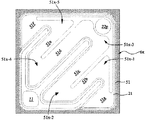
本発明の特徴である電極層の開口部21bの周期構造と、その上部に設けられる上部電極22の延伸部22aとの関係において、図2(a),(b)に示すように、開口部21bが少なくとも2つの軸33a,33bについて、周期的に2次元配列されており、その周期構造の基本単位格子Bの格子点に円形状の開口部21bが設けられている。このとき、周期構造の2軸33と、第2電極20の延伸部22aの延伸方向32とが、互いに異なる方向にあることで、下部、上部電極の延伸方向、開口部21bの軸(形成部21aの経路方向34)との重なりあわせにより、発光構造部51の上において、様々な面内方向への電流拡散を促し、また互いに補完して面内の様々な方向への電流拡散が可能となり、さらに、電極層21の開口部21bの軸方向が互いに直交せずに傾斜することで、直交する場合(図1)に問題となっていた電極間における経路長の差を小さくでき、上部電極22及び延伸部22aの各点における経路差を小さくでき、また、電極端部40,30の間隔が変化し、その端部方向41,31が互いに平行でなく傾斜している電極構造においては、その対向方向35が発光構造部51の面内において、延伸部、電極端部の各点において様々に変化するが、そのような電極構造においてこの実施形態に示すような開口部21bの周期構造をとることで、好ましい電流拡散が実現される。ここで、下部電極21の開口部21bの2次元周期構造は、図2に観るように、傾斜した軸33a,bにおいて、基本単位Bが周期的に配列された構造となる。   As shown in FIGS. 2 (a) and 2 (b), in relation to the periodic structure of the opening 21b of the electrode layer, which is a feature of the present invention, and the extended portion 22a of the upper electrode 22 provided thereabove, as shown in FIGS. 21b is periodically two-dimensionally arranged on at least two axes 33a and 33b, and circular openings 21b are provided at lattice points of the basic unit cell B of the periodic structure. At this time, since the biaxial axis 33 of the periodic structure and the extending direction 32 of the extending part 22a of the second electrode 20 are in different directions, the extending direction of the lower and upper electrodes, the axis of the opening 21b (formation part) By overlapping with the path direction 34) of 21a, the current diffusion in various in-plane directions is promoted on the light emitting structure 51, and the current diffusion in various in-plane directions can be complemented with each other. Furthermore, since the axial directions of the openings 21b of the electrode layer 21 are not orthogonal to each other, the difference in path length between the electrodes, which has been a problem when orthogonal (FIG. 1), can be reduced. In the electrode structure in which the path difference at each point of 22 and the extending portion 22a can be reduced, the interval between the electrode end portions 40 and 30 is changed, and the end direction 41 and 31 are not parallel to each other but inclined. Its facing direction 35 In the plane of the light emitting structure 51, it changes variously at each point of the extending portion and the electrode end, but it is preferable to take the periodic structure of the opening 21b as shown in this embodiment in such an electrode structure. Current spreading is realized. Here, the two-dimensional periodic structure of the opening 21b of the lower electrode 21 is a structure in which the basic units B are periodically arranged on the inclined axes 33a and 33b as seen in FIG.

実施形態2.(図3)
本発明に係る実施形態2として、図3に示すように、図2に比して開口部21bの形状を円形状から三角形状とし、その開口部21bが2つの異なる向きに形成されている点で異なる。
Embodiment 2. FIG. (Figure 3)
As Embodiment 2 which concerns on this invention, as shown in FIG. 3, compared with FIG. 2, the shape of the opening part 21b is changed from the circular shape to the triangular shape, and the opening part 21b is formed in two different directions. It is different.

このような電極層21の開口部21b形状、周期構造では、実施形態1と同様に、互いに平行でない傾斜した2軸33a,33bの周期構造を有し、その軸方向が、形成部21aの経路方向34にほぼ一致して設けられる。このような周期構造は、図1の直行する2軸の周期構造に比して、互いに傾斜した開口部21bの配列、形成部21aの経路方向34が設けられるため、上述したように、電極間の方向、電極端部30,40間の対向方向、各電極10,20の電極端部30,40の延伸方向31、延伸部22aの延伸方向と電極端部40の方向41若しくは対向方向とが、様々な方向に形成される場合において、実施形態1と同様に、好適に電極層21において電流拡散が実現される。また、周期構造の基本単位B内に2つの開口部21bが設けられており、それらを囲むように、軸方向33a,b,cにほぼ平行な経路方向34が設けられる。また周期構造の軸33は、33aと33bの他に、その間に33cが設けられる。   In the shape of the opening 21b and the periodic structure of the electrode layer 21 as described in the first embodiment, the electrode layer 21 has a periodic structure of two biaxial axes 33a and 33b that are not parallel to each other, and the axial direction thereof is the path of the forming portion 21a. It is provided substantially coincident with the direction 34. Such a periodic structure is provided with an array of openings 21b inclined with respect to each other and the path direction 34 of the forming portion 21a as compared with the biaxial periodic structure perpendicular to FIG. Direction, the opposing direction between the electrode end portions 30 and 40, the extending direction 31 of the electrode end portions 30 and 40 of each electrode 10 and 20, the extending direction of the extending portion 22a and the direction 41 or opposing direction of the electrode end portion 40a. In the case of being formed in various directions, current diffusion is preferably realized in the electrode layer 21 as in the first embodiment. In addition, two openings 21b are provided in the basic unit B of the periodic structure, and a path direction 34 substantially parallel to the axial directions 33a, b, and c is provided so as to surround them. The axis 33 of the periodic structure is provided with 33c between 33a and 33b.

実施形態3.(図4)
本発明に係る実施形態3として、図4に示すように、六角形状に開口部21bが設けられ、互いに形成部21aを介して配列されることから、基本単位Bには、様々な方向の形成部21aの経路方向34が形成される。実施形態1,2とは異なり、軸方向33と形成部21aの経路方向34とは一致せずに、複数の経路方向34でもって電極間35の経路36が形成され、例えば経路36cでは軸方向33a〜cのそれぞれと同じ方向の経路方向34で構成され、このように、面内のどの方向に延びる経路36であっても、複数の経路方向34による経路(形成部21a−1〜−6)で構成されることで、面内で比較的等方的な電流拡散が実現される。ここで、周期構造は、ほぼ正六角形状の開口部21bが3つ分有する基本単位Bとして設けられ、その単位B内に経路方向34が6方向に開口部21b間に設けられた形成部21aとして形成されている。
Embodiment 3. FIG. (Fig. 4)
As Embodiment 3 which concerns on this invention, as shown in FIG. 4, since the opening part 21b is provided in hexagonal shape and it mutually arranges via the formation part 21a, in the basic unit B, formation of various directions is carried out. A path direction 34 of the portion 21a is formed. Unlike the first and second embodiments, the axial direction 33 and the path direction 34 of the forming portion 21a do not coincide with each other, and a path 36 between the electrodes 35 is formed in a plurality of path directions 34. For example, the path 36c has an axial direction. 33a to 33c are configured in the same route direction 34, and thus the route 36 extending in any direction in the plane is formed by a plurality of route directions 34 (formers 21a-1 to -6). ) To achieve relatively isotropic current diffusion in the plane. Here, the periodic structure is provided as a basic unit B having three substantially hexagonal openings 21b, and a forming portion 21a in which the path direction 34 is provided between the openings 21b in six directions in the unit B. It is formed as.

実施形態4.(図6,9)
本発明に係る実施形態4として、図6,9に示すように、第1,2の電極10,20が、互いに対向して延伸する領域(発光構造部51)を有し、特に複数(発光構造部51a〜j)有しており、また、これら発光構造部51はそれぞれ電極延伸部12b,22bで挟まれて形成され、この挟まれた領域51a〜jにおいて下部電極層21が設けられる。このような発光構造部51は、それを挟む延伸部12b,22b(2次延伸部)を形成するために、すなわち、各延伸部12b−1〜−5(22b−5)間、両電極の延伸部12bと22b間に間隔を設けるように、延伸部の間に介在して延伸する1次延伸部12a,22aが設けられる。すなわち、各電極の台座部11,22pを基点として、各発光構造部51a〜jの幅方向若しくは長手方向に交叉する方向、上記両電極の対向延伸部12b,22bの延伸方向に交叉する方向に、延伸して設けられ、その1次延伸部12a,22aの任意の点を基点として、延伸させることで対向配置される2次延伸部12b,22bに連結される。また、対向して並行する延伸部間(12aと22b、22bと12b、12bと22a)の発光構造部51a〜cの他に、該延伸部の端部12z(22z)において、それを囲む他方電極20(10)の周縁電極部22x(12x)との間にあり、各発光構造部51a〜c間を連結する周縁電極部22x(12x)の発光構造部51x(51x−1,51x−2)が設けられている。また、上記実施形態1〜3(図2〜4)と同様に、また、図9についても同様に、台座部11,22pの対向部の電極端部40x,30xにおいて、他方電極20,10の対向部(延伸部22,12)の電極端部30a,bとの距離が電極位置により大きく異なる部分を有している。また、上記実施形態1〜3(図2〜4)と同様に、延伸部12b−2(22b−2)は湾曲しており、電極間距離がその位置により異なり、互いに平行しない電極延伸部12(22)が形成されている。
Embodiment 4 FIG. (Figs. 6 and 9)
As Embodiment 4 according to the present invention, as shown in FIGS. 6 and 9, the first and second electrodes 10 and 20 each have a region (light emitting structure 51) extending opposite to each other, and in particular, a plurality of (light emitting components). The light emitting structure portions 51 are formed by being sandwiched between the electrode extension portions 12b and 22b, respectively, and the lower electrode layer 21 is provided in the sandwiched regions 51a to 51j. Such a light emitting structure 51 is formed in order to form extended portions 12b and 22b (secondary extended portions) sandwiching the light emitting structure portion 51, that is, between the extended portions 12b-1 to -5 (22b-5). Primary extending portions 12a and 22a extending between the extending portions are provided so as to provide an interval between the extending portions 12b and 22b. That is, with the base portions 11 and 22p of each electrode as a base point, in the direction crossing in the width direction or the longitudinal direction of each light emitting structure 51a-j, in the direction crossing in the extending direction of the opposing extending portions 12b and 22b of both electrodes It is provided by being stretched, and is connected to secondary stretched portions 12b and 22b that are arranged opposite to each other by stretching from any point of the primary stretched portions 12a and 22a. In addition to the light emitting structure portions 51a to 51c between the extending portions (12a and 22b, 22b and 12b, 12b and 22a) that face each other in parallel, the other end that surrounds the other end portion 12z (22z) of the extending portion Light emitting structure portions 51x (51x-1, 51x-2) of the peripheral electrode portions 22x (12x) that are between the peripheral electrode portions 22x (12x) of the electrode 20 (10) and connect the light emitting structure portions 51a to 51c. ) Is provided. In addition, in the same manner as in the first to third embodiments (FIGS. 2 to 4) and also in FIG. 9, the electrode ends 40x and 30x of the facing portions of the pedestal portions 11 and 22p have the other electrodes 20 and 10 in the same manner. There are portions where the distance from the electrode end portions 30a, b of the facing portions (extending portions 22, 12) varies greatly depending on the electrode position. Further, as in the first to third embodiments (FIGS. 2 to 4), the extending portion 12b-2 (22b-2) is curved, the interelectrode distance differs depending on the position, and the electrode extending portions 12 that are not parallel to each other. (22) is formed.

図9に示す発光素子100では、各発光構造部51a〜jを挟む各電極の延伸部(2次延伸部)12b,22bは、互いに等間隔で、ほぼ平行に直進する、すなわち延伸部の延伸方向(31,41)、その対向端部の方向(32,42)がほぼ直線状である延伸部で構成されている。一方、図6では、発光構造部51bは、湾曲する延伸部12y−2、22y−2を2次延伸部12b−2,22b−2として、それに挟まれて形成され、その両側に隣接して設けられた発光構造部51b,cは、その湾曲する延伸部12y−2,22y−2と、直進する直線状の延伸部12b−1、22b−2とに挟まれて形成される。   In the light emitting device 100 shown in FIG. 9, the extending portions (secondary extending portions) 12b and 22b of the electrodes sandwiching the light emitting structure portions 51a to 51j go straight and substantially parallel to each other, that is, the extending portions extend. The direction (31, 41) and the direction (32, 42) of the opposite end portion are constituted by extending portions that are substantially linear. On the other hand, in FIG. 6, the light emitting structure 51 b is formed by sandwiching the extended portions 12 y-2 and 22 y-2 as the secondary extended portions 12 b-2 and 22 b-2 and adjacent to both sides thereof. The provided light emitting structure portions 51b and 51c are formed between the curved extending portions 12y-2 and 22y-2 and the linear extending portions 12b-1 and 22b-2 that advance straight.

このように、図9に観られるほぼ平行に直進する対向部では、その対向部における電極端部の延伸方向がほぼ平行で、それに傾斜する方向に軸方向を設けて周期的に配列された開口部21bが複数設けられた下部電極層21が形成される。   In this way, in the facing portion that is seen in FIG. 9 and that travels substantially parallel, the extending direction of the electrode end portion in the facing portion is substantially parallel, and the openings are periodically arranged with an axial direction in a direction inclined thereto. A lower electrode layer 21 having a plurality of portions 21b is formed.

また、図6,9の発光素子は、更に、一方電極10(20)の延伸部12(22)の端部12z(22z)を囲むように設けられる他方電極の台座部の端部、各発光構造部51a〜jを挟む延伸部の基点となる1次延伸部の端部により、周縁電極部22x(12x)が設けられ、その延伸端部12z(22z)と周縁電極部22x(12x)に挟まれた発光構造部51xが設けられている。この発光構造部51xは、並行する延伸部12と22に挟まれる各発光構造部51a〜jを連結させるように設けられる。このような連結部の発光構造部51xにおける両電極10,20の対向配置、特に一方の延伸端部12z(22z)と周縁電極部22x(12x)との配置関係は、図2〜4に見られる第1電極10と第2電極の延伸部12aとの配置関係と同様に、一方の電極延伸部が2方向に延伸して他方電極(延伸端部12z,22z)を囲み、両電極間に発光構造部51xが設けられる。更に、その領域51xにおいて、延伸部(周縁電極)12x(22x)は、他方電極を囲んで互いに異なる方向に延伸し、且つ、複雑な対向部の電極端部(周縁部12x,22x、台座部の対向する端部)が設けられる。このため、上述したように、この発光構造部51xに設けられる下部電極層21の開口部21b、形成部21aの周期構造は、同様に、互いに直交しない軸方向33(33a〜c)が、延伸方向34(32)、対向方向35に傾斜して、異なる方向とすることで、この発光構造部51xにおいて好適な電流拡散、発光が実現される。   Moreover, the light emitting element of FIGS. 6 and 9 further includes the end portion of the base portion of the other electrode provided so as to surround the end portion 12z (22z) of the extending portion 12 (22) of the one electrode 10 (20), and each light emission. A peripheral electrode portion 22x (12x) is provided by an end portion of a primary extending portion that becomes a base point of the extending portion sandwiching the structure portions 51a to 51j, and the extending end portion 12z (22z) and the peripheral electrode portion 22x (12x) A sandwiched light emitting structure 51x is provided. The light emitting structure portion 51x is provided so as to connect the light emitting structure portions 51a to 51j sandwiched between the extending portions 12 and 22 in parallel. The opposing arrangement of the electrodes 10 and 20 in the light emitting structure portion 51x of such a connecting portion, particularly the arrangement relationship between one extended end portion 12z (22z) and the peripheral electrode portion 22x (12x) is shown in FIGS. As in the arrangement relationship between the first electrode 10 and the extending portion 12a of the second electrode, one electrode extending portion extends in two directions and surrounds the other electrode (the extending end portions 12z and 22z), and between the two electrodes. A light emitting structure 51x is provided. Further, in the region 51x, the extended portion (peripheral electrode) 12x (22x) extends in different directions surrounding the other electrode, and the electrode ends (peripheral portions 12x and 22x, pedestal portions) of complex opposing portions Opposite ends). Therefore, as described above, the opening 21b of the lower electrode layer 21 provided in the light emitting structure 51x and the periodic structure of the forming portion 21a are similarly stretched in the axial directions 33 (33a to 33c) that are not orthogonal to each other. By tilting in the direction 34 (32) and the facing direction 35 to be different directions, suitable current diffusion and light emission are realized in the light emitting structure 51x.

ここで、図9(a)〜(c)の各例では、それぞれ、発光構造部51の数、間隔(幅)が異なり、また、延伸部12a,b(22a,b)の形状が異なる例である。具体的には、図9(c)には、上記実施形態1〜3と同様に、正負電極10,20(22)間に挟まれないで、電極(延伸部22)よりも素子の外側に発光構造部51xを有している。図9(a),(b)と(c)とでは、発光構造部51の個数、対向して並行に配置された延伸部12,22の対の数が異なり、(c)の形態が多く、また、図9(a)と(b)とでは、第1,2電極10,20の延伸部形状をほぼ反対としたものである。また上記実施形態1〜3、及び図6の形態と同様に、一方の電極10(20)の電極周縁部12x(22x)と他方電極20(10)の延伸部の延伸端部22z(12z)とに挟まれた発光構造部51xが、並行延伸部間の各発光構造部51a〜j間を連結するように配置されている。この周縁電極部における発光構造部51xについては、上述の通りである。また、図中には、周期構造の軸方向33、経路方向34、延伸部、電極端部の方向31,32(41,42)については符号を付していないが、図6,2〜4などと同様にしてその方向が決定されることはいうまでもない。
(第2電極20の上部電極22と下部電極層21の関係と、第1電極10との関係)
本発明の特徴部である第2電極20の下部電極層21における開口部21bの周期構造と、上部電極22の延伸部12aとの関係など、第1,2電極20との対向関係(対向電極間35)などについて詳細に説明する。これらは、上述したかく実施形態の素子構造、電極構造、延伸部構造に適用できる。
Here, in each example of FIGS. 9A to 9C, the number and interval (width) of the light emitting structure portions 51 are different, and the shapes of the extending portions 12a and b (22a and b) are different. It is. Specifically, in FIG. 9C, as in the first to third embodiments, the electrode is not sandwiched between the positive and negative electrodes 10 and 20 (22), and is located on the outer side of the element than the electrode (extension portion 22). It has a light emitting structure 51x. 9 (a), 9 (b) and 9 (c), the number of light emitting structure portions 51 and the number of pairs of extending portions 12 and 22 arranged in parallel opposite to each other are different, and there are many forms of (c). Also, in FIGS. 9A and 9B, the shapes of the extending portions of the first and second electrodes 10 and 20 are substantially reversed. Further, similarly to Embodiments 1 to 3 described above and FIG. 6, the electrode peripheral portion 12x (22x) of one electrode 10 (20) and the extending end 22z (12z) of the extending portion of the other electrode 20 (10). The light emitting structure 51x sandwiched between the light emitting structures is arranged so as to connect the light emitting structures 51a to 51j between the parallel extending portions. The light emitting structure portion 51x in the peripheral electrode portion is as described above. Further, in the drawing, the axial direction 33 of the periodic structure, the path direction 34, the extending portion, and the electrode end portions 31, 32 (41, 42) are not denoted by reference numerals, but FIGS. Needless to say, the direction is determined in the same manner as described above.
(Relationship between the upper electrode 22 and the lower electrode layer 21 of the second electrode 20 and the relationship with the first electrode 10)
The opposing relationship with the first and second electrodes 20 (counter electrode), such as the relationship between the periodic structure of the opening 21b in the lower electrode layer 21 of the second electrode 20 and the extended portion 12a of the upper electrode 22, which is a feature of the present invention. The interval 35) will be described in detail. These can be applied to the element structure, electrode structure, and extended portion structure of the embodiment described above.

本発明の発光素子100は、図8,13などに示すように、素子の積層構造101に、素子動作部57として、第1導電型層1の露出部1sに電極形成部52と、発光構造部51が、電極形成面側に好ましくはそれぞれ分離されて設けられ、図2〜4,6,9に示すように、発光構造部51の第2導電型層2の露出部2sを覆って、第2電極20の下部電極層21が形成され、その上に電気的に接続された上部電極22が設けられる。この上部電極22には、少なくとも延伸部22aが設けられて、少なくとも異なる2方向に延伸方向32(32a,32b)を、若しくは第1電極10との対向する電極の端部30(30a,30b)の延伸方向31(31a,31b)でもって、形成されている。   As shown in FIGS. 8 and 13 and the like, the light emitting device 100 of the present invention includes, as the device operating portion 57, the electrode forming portion 52 in the exposed portion 1 s of the first conductivity type layer 1, and the light emitting structure. The part 51 is preferably provided separately on the electrode forming surface side, and covers the exposed part 2s of the second conductivity type layer 2 of the light emitting structure part 51 as shown in FIGS. A lower electrode layer 21 of the second electrode 20 is formed, and an electrically connected upper electrode 22 is provided thereon. The upper electrode 22 is provided with at least an extending portion 22a, extending in at least two different directions in the extending direction 32 (32a, 32b), or the end 30 (30a, 30b) of the electrode facing the first electrode 10. It is formed in the extending direction 31 (31a, 31b).

このとき、図2〜4に示すように、互いに直交せずに90°方向から傾斜した少なくとも2軸33(33a,33b)の周期構造で2次元配列された開口部21b、開口部21b間に介在する形成部21a(経路34)を有している。この周期構造の軸33と、上記延伸方向32(31)とが、傾斜して互いに異なる方向とすることで、上部電極22の延伸部により線上、若しくは、第1電極10に対向して、対向する電極端部30が第1電極10の対向する端部40若しくはその延伸方向41に並行して、又は第1電極10の延伸部12の延伸方向42に並行して、形成されることで、面内に1次的に電流拡散が実施され、続いて、その下方で、上部電極22(延伸部12a)と発光構造部51(第2導電型層2)との間に設けられた層状の下部電極21により面内に広げられる際に、並行する第1電極(端部40、延伸部42)と上部電極22の延伸部12aとの間の発光構造部51a〜jにおいて、延伸部12aの延伸方向32、若しくは対向する電極端部30の延伸方向に傾斜して異なる方向に開口部21bが配列され、その開口部21b間に経路34(形成部21a)が設けられることで、電極間35に挟まれた発光構造部51a〜jにおいて、上記延伸方向32(31)とは異なる方向への面内の電流拡散が実現される。これにより、面内への電流拡散が好適なものとなり、また、開口部21bにより好適な光取出し、発光が可能となる素子100が得られる。   At this time, as shown in FIGS. 2 to 4, between the openings 21 b and the openings 21 b that are two-dimensionally arranged in a periodic structure of at least two axes 33 (33 a, 33 b) that are not orthogonal to each other and inclined from the 90 ° direction. It has the formation part 21a (path | route 34) which intervenes. The axis 33 of the periodic structure and the extending direction 32 (31) are inclined and different from each other, so that the extending portion of the upper electrode 22 is on the line or opposed to the first electrode 10. The electrode end 30 is formed in parallel with the opposing end 40 of the first electrode 10 or the extending direction 41 thereof, or in parallel with the extending direction 42 of the extending part 12 of the first electrode 10, First, current diffusion is performed in the plane, and subsequently, a layered structure provided between the upper electrode 22 (extension part 12a) and the light emitting structure part 51 (second conductivity type layer 2) is provided below. In the light emitting structure portions 51a to 51j between the parallel first electrodes (the end portion 40, the extending portion 42) and the extending portion 12a of the upper electrode 22 when being spread in the plane by the lower electrode 21, the extending portion 12a Stretching direction 32 or stretching of opposing electrode end 30 In the light emitting structure portions 51a to 51j sandwiched between the electrodes 35, the openings 21b are arranged in different directions and inclined, and the path 34 (formation portion 21a) is provided between the openings 21b. In-plane current diffusion in a direction different from the stretching direction 32 (31) is realized. As a result, the current diffusion into the surface becomes suitable, and the element 100 capable of taking out and emitting light appropriately through the opening 21b is obtained.

このとき、図2〜4,6,9に示すように、軸方向は、33aとbの他に、第3軸33cを備える形態、すなわち、互いに成す角がほぼ120°であるような場合でも良く、この場合、上記傾斜する2軸は3軸の内いずれかで上述したような面内への様々な方向への拡散が実現されるため、他の傾斜角の軸よりも好ましい。また周期構造の軸方向33は、主に開口部21bが隣接して配列される方向、若しくは開口部21b間に設けられる形成部21aの経路方向34に対して決定されるが、図4(b)に示すように、開口部21bが配列される方向は各軸を30°回転させた方向であるが、周期構造の基本単位Bを決定して、その単位Bの軸(辺)方向にとっても良い。また、軸方向は、図2〜4に示すように、その反対方向33a′、33b′、33c′にもとることができる。   At this time, as shown in FIGS. 2, 4, 6, and 9, the axial direction includes the third shaft 33 c in addition to 33 a and b, that is, even when the angle formed between each other is approximately 120 °. In this case, the two inclined axes are preferable to other inclined axes because diffusion in various directions into the plane as described above is realized by any one of the three axes. The axial direction 33 of the periodic structure is mainly determined with respect to the direction in which the openings 21b are arranged adjacent to each other or the path direction 34 of the forming portion 21a provided between the openings 21b. ), The direction in which the openings 21b are arranged is a direction in which each axis is rotated by 30 °. However, the basic unit B of the periodic structure is determined, and the axis (side) direction of the unit B is also determined. good. Further, as shown in FIGS. 2 to 4, the axial direction can be taken in the opposite directions 33a ′, 33b ′, and 33c ′.

図2〜4に示すように、開口部21b(形成部21a)の周期構造の基本単位Bは、周期構造の単位となる任意の大きさでとることができるが、好ましくは、最小面積で決定すると良い。図3に示すように、形成部21a上に単位Bをとる方法の他、図2に示すように開口部21bのほぼ中央を格子点とした単位Bとしても、図4に示すように、その両方を複合した単位Bとする方法のいずれでも良く、開口部21bの形状、その間の形状(形成部21a)により好適な単位Bが決定される。また、開口部と形成部は、周期構造において両者は反転された関係にあるため、開口部に関することは形成部に関することとして置き換えが可能であるが、少なくとも各開口部は互いに分離され、他方形成部は互いに連結されて形成される相違点をのぞくものである。また後述するように、開口部形成の製造上の問題から一部開口部がつぶれて形成されなかったり、隣接する開口部が繋がったり、形成部が一部分離されても、他の大部分が周期構造をとれば良く、またこのような製造上の形状不安定、位置ズレについても本発明の周期構造が適用される。   As shown in FIGS. 2 to 4, the basic unit B of the periodic structure of the opening 21 b (formation part 21 a) can be an arbitrary size as a unit of the periodic structure, but is preferably determined by the minimum area. Good. As shown in FIG. 3, in addition to the method of taking the unit B on the forming portion 21a, as shown in FIG. 4, the unit B having a lattice point at the approximate center of the opening 21b as shown in FIG. Any of the methods of combining both units B may be used, and a suitable unit B is determined by the shape of the opening 21b and the shape between them (formation portion 21a). In addition, since the opening and the forming portion are in an inverted relationship in the periodic structure, the opening can be replaced with the forming portion, but at least each opening is separated from each other and the other is formed. The parts except for the differences formed by being connected to each other. Also, as will be described later, even if some openings are not crushed due to manufacturing problems in forming the openings, adjacent openings are connected, or some of the formations are separated, most of the other parts are periodic. The periodic structure of the present invention is also applied to such manufacturing instability and positional deviation.

本発明のような周期構造の開口部21b、形成部21aは、図2〜4,6,9に示すように両電極10,20(延伸部)間における発光構造部51a〜jのほぼ全面に形成される形態が好ましいが、部分的に周期構造開口部が設けられ、他の部分が開口部を有さない電極21部とすること、他の部分が構造部51露出部とすることも可能である。また、上述したように、対向電極間の外部に位置する発光構造部51z、図2〜4では延伸部22と第1電極10との対向方向に反対方向の領域、においては、特に本発明のような周期構造とする必要が内が、発光の面内均一性、光取出し向上させることのために、同様な周期構造が形成されることが好ましい。   The opening portion 21b and the forming portion 21a having the periodic structure as in the present invention are formed on almost the entire surface of the light emitting structure portions 51a to 51j between the electrodes 10 and 20 (extension portions) as shown in FIGS. Although the formed form is preferable, it is also possible to provide a periodic structure opening partly, the other part may be an electrode part 21 having no opening part, and the other part may be a structure part 51 exposed part It is. In addition, as described above, the light emitting structure 51z located outside between the opposing electrodes, in FIGS. 2 to 4, in the region opposite to the opposing direction of the extending portion 22 and the first electrode 10, In order to improve the in-plane uniformity of light emission and the light extraction, it is preferable that a similar periodic structure is formed.

本発明は、上述したように電極間の構造部51における対向関係にある両電極10,20の延伸方向、例えば延伸部の延伸方向32(42)、対向部の電極端部30(40)の延伸方向31(41)と、その構造部51a〜jにおける電極層21の周期構造との関係が重要となり、対向関係を決める対向方向についても上記方向31,32(41,42)と同様である。また、本発明は、特に一方の電極(図2〜4では台座部11、図6,9では延伸部の端部12z、22z)を囲む他方電極の周縁電極(図2〜4では延伸部22、図6,9では周縁部22x、12x)構造(51x)において、さらには、それらの電極間距離、傾斜する方向が変化し、またその端部方向31,32(41,42)が互いに異なる複雑な電極構成、さらにはそれに加えて台座部端部30x、40xとの関係が複雑な電極構造部を有する(図6,9では一部51xとして有する)場合に特に有用である。   In the present invention, as described above, the extending direction of the electrodes 10 and 20 in the opposing relationship in the structure part 51 between the electrodes, for example, the extending direction 32 (42) of the extending part, and the electrode end 30 (40) of the opposing part. The relationship between the stretching direction 31 (41) and the periodic structure of the electrode layer 21 in the structure portions 51a to j is important, and the facing direction that determines the facing relationship is the same as the directions 31 and 32 (41, 42). . Further, the present invention particularly relates to the peripheral electrode of the other electrode (the extended portion 22 in FIGS. 2 to 4) surrounding one electrode (the pedestal portion 11 in FIGS. 2 to 4, and the end portions 12 z and 22 z of the extended portion in FIGS. 6 and 9). 6 and 9, in the peripheral portions 22x, 12x) structure (51x), the distance between the electrodes and the direction of inclination change, and the end directions 31, 32 (41, 42) are different from each other. This is particularly useful when the electrode structure has a complicated electrode structure and a complicated relationship with the base end portions 30x and 40x (partly 51x in FIGS. 6 and 9).

また、上記電極端部30,40との間において、対向方向35と、下部電極21の周期構造の2軸についても上記と同様に、異なる方向、互いに直交しない方向とすることで、好適な電流拡散が発光構造部51aにおいて実現される。   In addition, the opposite direction 35 and the two axes of the periodic structure of the lower electrode 21 between the electrode end portions 30 and 40 are different from each other in the same manner as described above, so that a suitable current can be obtained. Diffusion is realized in the light emitting structure 51a.

また、発光構造部51の上を覆って形成され、構造部51面内に電流拡散させる下部電極21、上部電極22とについては、上下関係は、例えば、線上の延伸部22とその上を覆って下部電極21が設けられる形態とすることもできる。すなわち、上部電極がそれよりも幅広、大面積の下部電極に電気的に接続されて両者の働きでもって、構造部51面内に電流拡散される構造を有することであり、好ましくは、台座部22pが一部に設けられた上部電極22の下方に下部電極が設けられることで、まず延伸部22a,bによる電流拡散から始まり好ましい。   In addition, regarding the lower electrode 21 and the upper electrode 22 that are formed so as to cover the light emitting structure 51 and diffuse the current in the surface of the structure 51, the vertical relationship is, for example, that the extended portion 22 on the line and the upper portion thereof are covered. The lower electrode 21 may be provided. That is, the upper electrode is electrically connected to the lower electrode having a wider and larger area and has a structure in which current is diffused in the surface of the structure portion 51 by the action of both, and preferably, the pedestal portion It is preferable that the lower electrode is provided below the upper electrode 22 in which 22p is provided in part, so that the current diffusion is first started by the extending portions 22a and 22b.

このように、第1段階として上部電極の延伸部22(12)及びその延伸方向32、電極端部30の延伸方向31に電流拡散されて、それに電気的に接続された下部電極層21の形成部21a(経路方向34)により拡散される。また台座部は図2〜4,6,9に観るように、延伸部よりも幅広な形状としても良く、パッド部として機能するように延伸部の幅を広くしてその任意の位置を台座部としても良く、図10などに示すように、ワイヤーボンディングされずに、電極形成面で基体104などに実装される場合には特に台座部の形状を他の部分(延伸部)と異なるような形状としなくても良い。また、台座部22p(上部電極)は、図1〜4に示すように、その形成部だけで設けられた形成部21pに設けられるような形態でも良く、図示しないが、上部電極で覆われる領域にも開口部21bが設けられる形態でも良い。   As described above, as the first step, the lower electrode layer 21 formed by current diffusion in the extending portion 22 (12) of the upper electrode and its extending direction 32 and the extending direction 31 of the electrode end 30 and electrically connected thereto. It is diffused by the part 21a (path direction 34). 2-4, 6 and 9, the pedestal portion may have a shape wider than the extending portion, and the extending portion is widened so as to function as a pad portion, and the pedestal portion is positioned at an arbitrary position. As shown in FIG. 10 and the like, the shape of the pedestal portion is different from other portions (extension portions) particularly when mounted on the base 104 or the like on the electrode forming surface without wire bonding. You don't have to. Further, as shown in FIGS. 1 to 4, the pedestal portion 22 p (upper electrode) may be provided in the forming portion 21 p provided only by the forming portion, and is not shown, but is a region covered with the upper electrode. Alternatively, the opening 21b may be provided.

また、上部電極22と下部電極21との関係は、上述したように、上部電極において部分的な領域に好適に電流が拡散・供給される配線電極としての役目を果たせばよいため、好ましくは下部電極21よりもシート抵抗が小さくなるように上部電極22(延伸部22a,b)が設けられる。具体的には、下部電極21よりも大きな膜厚で上部電極22(延伸部22a,b)が形成され、特に下部電極21の形成部21aが透光性である場合には好ましい。また、下部電極21の形成部21aが透光性である場合には、上部電極22(延伸部22a,b)よりも透過率が高くなるように形成されることで、各電極の機能、電流拡散と光取出しをそれぞれ異なるものとでき、好適な電極構造が得られ好ましい。また、後述するように、透光性電極(形成部21a)の上に別途反射膜を設ける場合についても透光性の形成部21aと同様の条件が好ましい。他方、電極形成部21aを反射性の電極とする場合には、上述した関係にとらわれず、適宜各特性の電極21,22を形成すると良い。   Further, as described above, the relationship between the upper electrode 22 and the lower electrode 21 is preferably the lower electrode because it can serve as a wiring electrode in which current is suitably diffused and supplied to a partial region in the upper electrode. The upper electrode 22 (extending portions 22a and 22b) is provided so that the sheet resistance is smaller than that of the electrode 21. Specifically, the upper electrode 22 (extension portions 22a and 22b) is formed with a film thickness larger than that of the lower electrode 21, and is particularly preferable when the formation portion 21a of the lower electrode 21 is translucent. In addition, when the formation portion 21a of the lower electrode 21 is translucent, the function and current of each electrode can be increased by forming the lower electrode 21 so that the transmittance is higher than that of the upper electrode 22 (extension portions 22a and b). Diffusion and light extraction can be made different from each other, and a preferable electrode structure is obtained. Further, as will be described later, the same conditions as those for the translucent forming portion 21a are preferable when a reflective film is separately provided on the translucent electrode (forming portion 21a). On the other hand, when the electrode forming portion 21a is a reflective electrode, the electrodes 21 and 22 having various characteristics may be appropriately formed regardless of the above-described relationship.

(本発明の発光素子100)
以上説明した各実施形態において、その実施形態(発光素子100)の各構成について以下に詳しく、説明するが、本発明は上記実施形態及びその構成について組み合わせて適用することもできる。また、上記実施形態及びそれを説明する各図面、並びに後述する各構成の説明及びその図面の符号は共通しており、また一部誇張して描画されているものもある。
(素子構造体101)
本発明の発光素子100に用いられる素子構造体101は、図8,13の断面図などに示すように、基板4上に、第1導電型層1、活性層(発光層3)、第2導電型層2が順に積層された積層構造体101でもよく、第1,2導電型層1,2が横方向に接合されていてもよく、これらを組み合わせたもの、例えば断面が折れ線(連続直線)状、山形、谷形などの様々な面が複合された接合面、でもよい。
(Light Emitting Element 100 of the Present Invention)
In each embodiment described above, each configuration of the embodiment (light emitting element 100) will be described in detail below, but the present invention can also be applied in combination with the above embodiment and the configuration. In addition, the above-described embodiment and the drawings for explaining the same, the description of each configuration to be described later, and the reference numerals of the drawings are common, and some are exaggerated and drawn.
(Element structure 101)
The element structure 101 used in the light emitting element 100 of the present invention includes a first conductivity type layer 1, an active layer (light emitting layer 3), a second layer on a substrate 4 as shown in the cross-sectional views of FIGS. The laminated structure 101 in which the conductive type layers 2 are sequentially laminated may be used, or the first and second conductive type layers 1 and 2 may be joined in the lateral direction. It may be a joint surface in which various surfaces such as a shape, a mountain shape, and a valley shape are combined.

具体的には、本発明の発光素子100は、素子構造体101として、図8,13に示すように、素子構造体101は、基板4上に、第1導電型層1、発光層(活性層)3、第2導電型層2が順に積層された積層構造101を有するものであり、このとき、電極形成面内において、発光構造部51は、図に示すように積層方向に第1,2導電型層が発光層を挟む構造の他、上述したとおり、第1,2導電型層が横方向に接合されていてもよく、またこれらを組み合わせた縦、横の複雑な複合接合面を形成したものでもよい。また、発光素子構造として、MIS構造、p−n接合構造、ホモ接合構造、ヘテロ接合構造(ダブルヘテロ構造)、PIN構造などを用いることができ、またユニポーラ素子にも適用できるが、好ましくは、第1,2導電型層が互いに異なる導電型層となるp−n接合構造などのn型、p型層で活性層を挟む構造を用いることが好ましい。   Specifically, the light emitting device 100 of the present invention is an element structure 101 as shown in FIGS. 8 and 13, and the device structure 101 is formed on the substrate 4 with the first conductivity type layer 1 and the light emitting layer (active layer). Layer) 3 and the second conductivity type layer 2 are sequentially laminated. At this time, within the electrode formation surface, the light emitting structure 51 includes first and second layers in the lamination direction as shown in the figure. In addition to the structure in which the two conductivity type layers sandwich the light emitting layer, as described above, the first and second conductivity type layers may be bonded in the horizontal direction, and a complex vertical and horizontal composite bonding surface combining these may be used. It may be formed. Further, as the light emitting element structure, a MIS structure, a pn junction structure, a homojunction structure, a heterojunction structure (double heterostructure), a PIN structure, or the like can be used, and it can also be applied to a unipolar element. It is preferable to use a structure in which the active layer is sandwiched between n-type and p-type layers such as a pn junction structure in which the first and second conductivity-type layers are different conductivity-type layers.

素子構造体100を構成する積層構造の半導体材料は、InAlGaP系材料、InP系材料、AlGaAs系材料、これらの混晶材料でもよく、GaN系窒化物半導体材料でもよい。GaN系窒化物半導体材料として具体的には、GaN、AlN、もしくはInN、又はこれらの混晶であるIII−V族窒化物半導体(InαAlβGa1−α−βN、0≦α、0≦β、α+β≦1)で表され、またこれに加えて、III族元素として一部若しくは全部にBを用いたり、V族元素としてNの一部をP、As、Sbで置換したりした混晶でもよい。以下、窒化物半導体を用いて説明するが、他の材料系にも適用される。 The semiconductor material having a laminated structure constituting the element structure 100 may be an InAlGaP-based material, an InP-based material, an AlGaAs-based material, a mixed crystal material thereof, or a GaN-based nitride semiconductor material. Specifically, as a GaN-based nitride semiconductor material, a group III-V nitride semiconductor (In α Al β Ga 1-α-β N, 0 ≦ α, GaN, AlN, InN, or a mixed crystal thereof) 0 ≦ β, α + β ≦ 1), and in addition to this, B is used as part or all of the group III element, or part of N is substituted with P, As, or Sb as the group V element. Mixed crystals may be used. Hereinafter, a nitride semiconductor will be used for explanation, but the present invention can be applied to other material systems.

発光層としては、InGaN系材料を用いることができ、ワイドバンドギャップの発光層により、緑色、青色の可視光域から紫色、それより短波長の紫外域に発光するものが得られる。   As the light emitting layer, an InGaN-based material can be used, and a light emitting layer having a wide bandgap can emit light that emits light from a green or blue visible light region to a purple or shorter wavelength ultraviolet region.

各実施形態では、第1,2導電型層1,2を、n型層、p型層としているが、この逆でも良い。また、半導体積層構造101の成長方法として具体的にはMOVPE(有機金属気相成長法)、HVPE(ハライド気相成長法)、MBE(分子線エピタキシー法)、MOCVD(有機金属化学気相成長法)があり、好ましくはMOCVD,MBEである。   In each embodiment, the first and second conductivity type layers 1 and 2 are an n-type layer and a p-type layer, but this may be reversed. Further, as a growth method of the semiconductor laminated structure 101, specifically, MOVPE (metal organic chemical vapor deposition), HVPE (halide vapor deposition), MBE (molecular beam epitaxy), MOCVD (metal organic chemical vapor deposition). ), Preferably MOCVD, MBE.

本発明の半導体積層構造101の成長方法に用いる基板、特にエピタキシャル成長用の基板10としては、窒化物半導体と異なる材料の異種基板として、例えば、C面、R面、及びA面のいずれかを主面とするサファイア、スピネル(MgA124)のような絶縁性基板、SiC(6H、4H、3Cを含む)、ZnS、ZnO、GaAs、Si、及び窒化物半導体と格子整合する酸化物基板等、窒化物半導体を成長させることが可能で従来から知られており、窒化物半導体と異なる基板材料を用いることができ、好ましくはサファイア、スピネルであり、また異種基板以外として、GaN、AlNなどの窒化物半導体基板なども用いることができる。他の半導体材料においては従来知られた同じ材料系の基板、若しくはSiなどの異種基板を用いることができる。
(半導体積層構造101)
発光素子100を形成する半導体積層構造101としては、例えば図8,13,15,16に示すように、上記基板4上に下地層5などを介して成長され、このとき、下地層5を素子構造101として動作部に含めても良いが、通常素子構造の成長用のみ形成されて素子として機能しない非動作部として設けられる。下地層は、特に異種基板を用いた場合、結晶核形成、核成長層として、低温成長バッファ層を用い、好適な条件はAlxGa1-xN(0≦x≦1)を低温(200〜900℃)で成長させるものであり、続いて高温で層成長させて、膜厚50Å〜0.1μm程度(単結晶、高温成長層)で形成する。また、ELO(Epitaxial Lateral Overgrowth)として知られるように、基板上、若しくは下地層上に、島状部(凸部、マスク開口部)などの成長部を他の領域に比べて優先的、若しくは選択的に成長させて、各選択成長部が横方向に成長して接合、会合することで層を形成するような成長層を下地層5若しくは、素子積層構造101に用いることもでき、これにより結晶性、特に結晶欠陥を低減させた素子構造とできる。
As the substrate used for the growth method of the semiconductor multilayer structure 101 of the present invention, particularly the substrate 10 for epitaxial growth, for example, one of the C-plane, R-plane, and A-plane is mainly used as a heterogeneous substrate of a material different from the nitride semiconductor. Insulating substrate such as sapphire, spinel (MgA1 2 O 4 ), SiC substrate (including 6H, 4H, 3C), ZnS, ZnO, GaAs, Si, and an oxide substrate lattice-matched with a nitride semiconductor, etc. It is possible to grow a nitride semiconductor, and it has been conventionally known that a substrate material different from that of a nitride semiconductor can be used, preferably sapphire or spinel. A nitride semiconductor substrate or the like can also be used. As other semiconductor materials, conventionally known substrates of the same material system or different types of substrates such as Si can be used.
(Semiconductor laminated structure 101)
For example, as shown in FIGS. 8, 13, 15, and 16, the semiconductor multilayer structure 101 that forms the light emitting element 100 is grown on the substrate 4 via the base layer 5. Although it may be included in the operating portion as the structure 101, it is provided only as a non-operating portion that is usually formed only for growth of the element structure and does not function as an element. In particular, when a different substrate is used as the underlayer, a low-temperature growth buffer layer is used as a crystal nucleation and nucleation layer, and preferable conditions are Al x Ga 1-x N (0 ≦ x ≦ 1) at a low temperature (200 ˜900 ° C.), followed by layer growth at a high temperature to form a film with a thickness of about 50 to 0.1 μm (single crystal, high temperature growth layer). Further, as known as ELO (Epitaxial Lateral Overgrowth), a growth portion such as an island-shaped portion (convex portion, mask opening portion) is preferentially selected or selected as compared with other regions on a substrate or an underlying layer. It is also possible to use a growth layer for forming the layer by growing each of the selective growth portions in the lateral direction to form a layer by joining and associating with each other. And, in particular, an element structure with reduced crystal defects.

窒化物半導体に用いるドーパントとして、n型不純物としては、Si、Ge、Sn、S、O、Ti、Zr等のIV族、若しくはVI族元素を用いることができ、好ましくはSi、Ge、Snを、さらに最も好ましくはSiを用いる。また、p型不純物としては、特に限定されないが、Be、Zn、Mn、Cr、Mg、Caなどが挙げられ、好ましくはMgが用いられる。これら、アクセプター、ドナーの各ドーパントを添加することにより、各導電型の窒化物半導体層を形成し、後述する各導電型層を構成する。また、窒化物半導体は不純物をドープしない無添加層であってもn型層として用いることができ、さらにAlGaAsなどの他の材料系にはそれに適したドーパント用いる。本発明における第1導電型層、第2導電型層には、部分的にアンドープの層、半絶縁性の層が積層されていても良く、電流阻止層のよう逆導電型の埋込層に、各導電型層内に部分的に寄生な素子部分を形成していても良い。
(第1導電型層1)
上記実施形態の素子構造で示すように、第1導電型層1として、各導電型のドーパントを含有させ、電極形成面内及び活性層へのキャリアの供給、拡散を実現するような層構造を形成すると良く、特に電極形成部52から発光構造部51にキャリアを面内に拡散して供給する電流拡散導体13(コンタクト層)には、他の領域より高濃度にドープされることが好ましい。また、このような電荷供給・面内拡散層(コンタクト層及びその近傍層)の他に、上記実施形態で示すように、積層方向において発光層へ電荷を移動・供給させる介在層、若しくは第2導電型のキャリアを発光層に閉じこめるクラッド層などを、コンタクト層とは別に設けることが好ましい。このような発光層3と面内拡散層(領域)のコンタクト層との間に設ける層として、窒化物半導体素子の場合には、面内拡散層(領域)より低濃度ドーパント量若しくはアンドープの低不純物濃度層(アンドープ層)、及び/又は多層膜層を設けることが好ましい。これは、低不純物層でもって、高不純物層(面内拡散層)による結晶性悪化を回復させてその上に成長させるクラッド層、発光層の結晶性を良好にし、駆動時にあっては高濃度層に隣接して低濃度層が設けられることで面内拡散を促進させ、また、耐圧性も向上させることができる。多層膜層は、少なくとも2種の層を交互に積層させたような周期構造で形成すること、具体的には、Inを含む窒化物半導体層とそれとは異なる組成の層の周期構造、好ましくはInxGa1-xN/InyGa1-yN(0<x<y<1)で構成することで、発光層、特にInを含む窒化物半導体層、好ましくはそれを井戸層として複数用いた場合において、その結晶性を向上させることができる。このような多層膜としては、組成が異なる層による周期構造の他、組成傾斜構造、また、これらの構造において不純物濃度を変調させた構造、膜厚を変動させた構造なども採用でき、好ましくは、20nm以下の膜厚の層を積層した構造、さらに好ましくは10nm以下の膜厚の層を積層した構造で形成することが、上記結晶性に有利となる。
(発光層[活性層)3)
本発明の素子構造101としては、第1,2導電型層との間に、発光層を設けて、発光層で発光させる素子構造とすることが好ましく、特に窒化物半導体においてはInを含む窒化物半導体を発光層に用いたものが、紫外域から可視光(赤色光)の領域において好適な発光効率が得られ好ましく、特にInGaN層を用いること、特にInの混晶比を変化させて所望の発光波長を得ることが好ましい。このほかの窒化物半導体材料として、GaN,AlGaNなどのInGaNよりも高バンドギャップの材料を用いて、紫外域において使用する発光素子としても良い。
As a dopant used for the nitride semiconductor, as an n-type impurity, a group IV or group VI element such as Si, Ge, Sn, S, O, Ti, or Zr can be used, and preferably Si, Ge, or Sn is used. Most preferably, Si is used. The p-type impurity is not particularly limited, and examples thereof include Be, Zn, Mn, Cr, Mg, and Ca, and Mg is preferably used. By adding these acceptor and donor dopants, nitride semiconductor layers of each conductivity type are formed, and each conductivity type layer described later is formed. A nitride semiconductor can be used as an n-type layer even if it is an additive-free layer not doped with impurities, and a dopant suitable for other material systems such as AlGaAs is used. In the first conductivity type layer and the second conductivity type layer in the present invention, a partially undoped layer or a semi-insulating layer may be laminated, and the reverse conductivity type buried layer such as a current blocking layer may be laminated. A partially parasitic element portion may be formed in each conductivity type layer.
(First conductivity type layer 1)
As shown in the element structure of the above embodiment, the first conductivity type layer 1 has a layer structure that contains dopants of each conductivity type and realizes supply and diffusion of carriers to the active layer and within the electrode formation surface. In particular, the current diffusion conductor 13 (contact layer) that diffuses and supplies carriers in the plane from the electrode forming portion 52 to the light emitting structure portion 51 is preferably doped at a higher concentration than other regions. In addition to such a charge supply / in-plane diffusion layer (contact layer and its neighboring layers), as shown in the above embodiment, an intermediate layer that moves and supplies charges to the light emitting layer in the stacking direction, or a second layer It is preferable to provide a clad layer or the like for confining conductive carriers in the light emitting layer separately from the contact layer. As a layer provided between the light emitting layer 3 and the contact layer of the in-plane diffusion layer (region), in the case of a nitride semiconductor element, the dopant concentration is lower than that of the in-plane diffusion layer (region) or the amount of undoped is lower. It is preferable to provide an impurity concentration layer (undoped layer) and / or a multilayer film layer. This is because the low impurity layer recovers the deterioration of crystallinity due to the high impurity layer (in-plane diffusion layer) and improves the crystallinity of the clad layer and the light emitting layer grown on it. By providing the low concentration layer adjacent to the layer, in-plane diffusion can be promoted and pressure resistance can be improved. The multilayer film layer is formed with a periodic structure in which at least two kinds of layers are alternately stacked, specifically, a periodic structure of a nitride semiconductor layer containing In and a layer having a different composition, preferably By comprising In x Ga 1-x N / In y Ga 1-y N (0 <x <y <1), a light emitting layer, particularly a nitride semiconductor layer containing In, preferably a plurality of well layers as well layers When used, the crystallinity can be improved. As such a multilayer film, in addition to a periodic structure composed of layers having different compositions, a composition gradient structure, a structure in which the impurity concentration is modulated in these structures, a structure in which the film thickness is changed, and the like can be adopted. It is advantageous for the crystallinity to form a structure in which layers with a thickness of 20 nm or less are stacked, and more preferably with a structure in which layers with a thickness of 10 nm or less are stacked.
(Light emitting layer [active layer) 3)
The element structure 101 of the present invention is preferably an element structure in which a light emitting layer is provided between the first and second conductivity type layers so that light is emitted from the light emitting layer. In particular, in a nitride semiconductor, nitride containing In is included. It is preferable that a light emitting layer is used for the light emitting layer because a suitable light emitting efficiency can be obtained in the ultraviolet to visible light (red light) region, and it is particularly desirable to use an InGaN layer, particularly by changing the mixed crystal ratio of In. It is preferable to obtain the emission wavelength. As another nitride semiconductor material, a material having a higher band gap than InGaN such as GaN and AlGaN may be used as a light emitting element used in the ultraviolet region.

さらに好ましい発光層としては、量子井戸構造の活性層を用いることであり、井戸層が1つの単一量子井戸構造、さらに好ましくは、複数の井戸層が障壁層を介して積層した構造の多重量子井戸構造を採用することが好ましい。井戸層については上記発光層と同様に、好ましくはInGaN層を用いることであり、障壁層として、井戸層よりバンドギャップエネルギーが大きくなるような層として、例えばInGaN、GaN、AlGaNを設けることが好ましい。このとき、井戸層、障壁層の膜厚としては、30nm以下、好ましくは20nm以下、さらに井戸層において好ましくは10nm以下とすることで、量子効率に優れた発光層が得られる。また、井戸層、障壁層に、各導電型層のドーパントがドープされていても良く、障壁層は、井戸層間に一層以上設けても良い。
(第2導電型層2)
第2導電型層2としては、キャリアを発光層に閉じこめるクラッド層、電極が形成されるコンタクト層を、設けることが好ましく、この時両層を別々に設けてコンタクト層をクラッド層よりも発光層より遠くに設け、高濃度にドーパントをドープすることが好ましい。窒化物半導体においては、クラッド層として好ましくはAlを含む窒化物半導体、さらに好ましくはAlGaN層を用いることが好ましく、さらに発光層に近接して、好ましくは接して形成されることで発光層の効率を高めることができ好ましい。さらに、コンタクト層とクラッド層との間にそれらの層より低不純物濃度の層を介在させることで、耐圧性に優れた素子とでき、またコンタクト層を高濃度にドープしても結晶性を改善できるため好ましい。コンタクト層は、図8,13に示すように、電極形成面内で発光部51として設けられるため、その面内でキャリアを拡散させる層としても機能しうるが、本発明では、電極20を設けて、該面内の一部に延伸する上部電極22と、それよりも面積の大きな、断面幅広な層状の下部電極21により面内での電流拡散導層、拡散導体として機能させることで、窒化物半導体における低い移動度のp型キャリアの拡散を補助し、また、コンタクト層の膜厚を他の層(クラッド層、介在低濃度層)よりも小さくして、且つ他の層よりも高濃度に不純物ドープすることで、高キャリア濃度の層を形成して、電極から良好な電荷注入を実現でき好ましい。
(電流拡散導体13)
このように本発明の積層構造101において、電流拡散導体13は、素子構造体内(第1導電型層内13)に設けられても、素子構造体上(の電極21)に設けられる形態でもよい。具体的には、図13などに示すように、第1導電型層1においては、露出電極形成面52に第1の電極10が設けられ、該第1電極10が設けられた第1導電型層10内を横方向に電流拡散する拡散導体13として機能し、他方、第2導電型層2側には、延伸電極に電気的に接合するオーミック接触用の電極21でもって、面内において、一部に設けられた電極延伸部から、電流を面内に広く拡散させる拡散導体として機能する。第2導電型層2内に拡散層を設けても良く、第1導電型層上に、外部(電極)の拡散導体を設けても良い。
(発光素子面内構造)
本発明において、発光素子構造101の電極形成面内の構造としては、図8,13に示すように、発光層3とそれを挟む第1,2導電型層1,2が形成された発光構造部51と、第1導電型層1側電極形成部52とを、面内で一部が重なる構造よりも分離して設けることが好ましい。本発明の発光素子は、素子構造部57に発光構造部51と電極形成部52が設けられた構造であり、素子構造部57は電流拡散導体13(第1導電型層1)上に形成され、1つの素子構造部57内で1つの発光構造部51(図2〜4,6,9)とする形態でも良く、1つの素子構造部57内で複数の発光構造部51が形成されるような発光構造部51の集積構造を形成しても良く、1つの素子構造57に対して少なくとも1対の発光構造部51と電極形成部52が形成されれば良く、さらに、素子構造部57を複数集積して集積型の発光素子100とすることもできる。
As a more preferable light emitting layer, an active layer having a quantum well structure is used. The multi-quantum has a structure in which the well layer is a single quantum well structure, and more preferably, a plurality of well layers are stacked via a barrier layer. It is preferable to employ a well structure. As for the well layer, an InGaN layer is preferably used similarly to the above light-emitting layer, and for example, InGaN, GaN, or AlGaN is preferably provided as a barrier layer that has a band gap energy larger than that of the well layer. . At this time, the thickness of the well layer and the barrier layer is 30 nm or less, preferably 20 nm or less, and more preferably 10 nm or less in the well layer, whereby a light emitting layer having excellent quantum efficiency can be obtained. Moreover, the dopant of each conductivity type layer may be doped to the well layer and the barrier layer, and one or more barrier layers may be provided between the well layers.
(Second conductivity type layer 2)
As the second conductivity type layer 2, it is preferable to provide a clad layer for confining carriers in the light emitting layer and a contact layer on which the electrode is formed. At this time, both layers are provided separately and the contact layer is more light emitting than the clad layer. It is preferable that the dopant is provided further away and the dopant is doped at a high concentration. In the nitride semiconductor, it is preferable to use a nitride semiconductor containing Al as the cladding layer, more preferably an AlGaN layer, and the efficiency of the light emitting layer by being formed close to, preferably in contact with, the light emitting layer. Can be improved. Furthermore, by interposing a layer with a lower impurity concentration between the contact layer and the clad layer, it is possible to obtain an element with superior pressure resistance, and crystallinity is improved even if the contact layer is highly doped This is preferable because it is possible. As shown in FIGS. 8 and 13, the contact layer is provided as the light emitting portion 51 in the electrode formation surface, and thus can function as a layer for diffusing carriers in the surface. In the present invention, the electrode 20 is provided. The upper electrode 22 extending partly in the plane and the layered lower electrode 21 having a larger area and a wider cross section than the upper electrode 22 function as an in-plane current diffusion conductive layer and diffusion conductor. Assists diffusion of low mobility p-type carriers in a physical semiconductor, and makes the contact layer thickness smaller than other layers (cladding layer, intervening low concentration layer) and higher in concentration than other layers Doping with impurities is preferable because a high carrier concentration layer can be formed and good charge injection can be realized from the electrode.
(Current diffusion conductor 13)
Thus, in the laminated structure 101 of the present invention, the current spreading conductor 13 may be provided in the element structure (in the first conductivity type layer 13) or on the element structure (in the electrode 21). . Specifically, as shown in FIG. 13 and the like, in the first conductivity type layer 1, the first electrode 10 is provided on the exposed electrode formation surface 52, and the first conductivity type in which the first electrode 10 is provided. The layer 10 functions as a diffusion conductor 13 for current diffusion in the lateral direction. On the other hand, on the second conductivity type layer 2 side, an ohmic contact electrode 21 that is electrically joined to the stretched electrode is used. It functions as a diffusion conductor that diffuses current widely in the plane from the electrode extension part provided in a part. A diffusion layer may be provided in the second conductivity type layer 2, and an external (electrode) diffusion conductor may be provided on the first conductivity type layer.
(Light emitting element in-plane structure)
In the present invention, the structure within the electrode formation surface of the light emitting element structure 101 is, as shown in FIGS. 8 and 13, a light emitting structure in which a light emitting layer 3 and first and second conductivity type layers 1 and 2 sandwiching the light emitting layer 3 are formed. It is preferable that the portion 51 and the first conductivity type layer 1 side electrode forming portion 52 are provided separately from a structure in which a part thereof overlaps in the plane. The light emitting element of the present invention has a structure in which the light emitting structure 51 and the electrode forming part 52 are provided in the element structure 57, and the element structure 57 is formed on the current diffusion conductor 13 (first conductivity type layer 1). A single light emitting structure 51 (FIGS. 2 to 4, 6, 9) may be used in one element structure 57, and a plurality of light emitting structures 51 may be formed in one element structure 57. An integrated structure of light emitting structure portions 51 may be formed, and at least one pair of light emitting structure portions 51 and electrode forming portions 52 may be formed with respect to one element structure 57. A plurality of integrated light-emitting elements 100 can also be obtained.

電極の形成形態としては、図2〜4,6,9に示すように、双方の電極の少なくとも一方が、延伸部、湾曲・屈曲する延伸部、台座部、を備えていてもよく、好ましくは第1導電型層2側に湾曲する延伸部22y、屈曲・湾曲する複合電極端部を有する周縁電極部22x(12x)を設けて、その電極(一方の台座部若しくは延伸端部12z[22z])間の発光構造部51を形成してそれを覆う下部電極層21で電流拡散させ、図6,9に示すように両方の電極に設けることもできる。また、図14(a)に示すように、複数の台座部が延伸方向に離間されて配置されていてもよく、延伸部が断続的に延伸していてもよく、この場合素子外部の例えば実装基体104、貼り合わせ用の転写基板9側の電極で分離された台座部が電気的に接続されて、全体として延伸電極として機能する。   As shown in FIGS. 2, 4, 6, and 9, at least one of both electrodes may be provided with an extending portion, an extending portion that bends and bends, and a pedestal portion, as shown in FIGS. An extending portion 22y that is curved toward the first conductivity type layer 2 side and a peripheral electrode portion 22x (12x) having a bent and curved composite electrode end portion are provided, and the electrode (one pedestal portion or the extended end portion 12z [22z]) is provided. ), The light emitting structure 51 is formed, and the current is diffused in the lower electrode layer 21 covering the light emitting structure 51, and the light emitting structure 51 is provided on both electrodes as shown in FIGS. Moreover, as shown to Fig.14 (a), the several base part may be arrange | positioned spaced apart in the extending | stretching direction, and the extending | stretching part may extend | stretch intermittently. The base portion separated by the electrode on the substrate 104 and the transfer substrate 9 side for bonding is electrically connected to function as a stretched electrode as a whole.

各電極の配線形態としては、各電極は素子構造体内に電流供給できるように、オーミック接触されたオーミック接触部を有することが好ましく、該オーミック接触部に一致して電極(延伸部、台座部)が形成されていることが好ましい。他の形態としては、離間して配置されたオーミック接触部に対して、それらを導通するように、配線用として電極が設けられてもよい。また、このような配線用電極は、後述する素子実装基体側に設けられてもよい。   As a wiring form of each electrode, it is preferable that each electrode has an ohmic contact portion that is in ohmic contact so that a current can be supplied into the element structure, and an electrode (extension portion, pedestal portion) that matches the ohmic contact portion. Is preferably formed. As another form, an electrode may be provided for wiring so as to conduct the ohmic contact portions arranged apart from each other. Moreover, such a wiring electrode may be provided on the element mounting substrate side described later.

電極形成部52としては、電極形成可能なように、第1導電型層1の露出部52(1s)に設けられ、該露出部は、図8に示すように、第1導電型層1、発光層3、第2導電型層2を順に積層した積層構造101において、第2導電型層2、発光層3の面内の一部、若しくはそれに加えて第1導電型層1の深さ方向の一部を除去して、露出させた露出部1sを電極形成部52とする他、図13(b)に示すように、分離溝52aを形成して、その溝52aを介して発光構造部51に離間させて、露出部1eから第2導電型層露出部に跨って電極10を形成して、電極形成部52を面内に設ける構造とすることもでき、また図13(a)に示すように、形成した第1導電型層1−1の面内一部を、除去若しくはマスクして、面内一部に発光構造部51として、発光層3、第2導電型層2、若しくはそれに加えて第1導電型層の一部2−3を積層成長させた構造を面内の一部(発光構造部)に形成する構造とすることもできる。このとき、電極10のボンディング位置である電極形成部52は、積層方向において、電極20と同等とすることも、それよりも高い位置とすることもできる。また、このとき、電極形成部52は、発光構造部51とは面内で分離されて形成されるので、電極形成部52の領域は非発光領域となり、発光構造部51と電極形成部52とに面内で重なって、下部に設けられた第1導電型層の一部領域の拡散部13などにより、電極10から発光構造部51にキャリアが面内拡散され供給される。   The electrode forming portion 52 is provided on the exposed portion 52 (1s) of the first conductivity type layer 1 so that an electrode can be formed. The exposed portion is formed of the first conductivity type layer 1, as shown in FIG. In the laminated structure 101 in which the light emitting layer 3 and the second conductivity type layer 2 are sequentially laminated, the depth direction of the first conductivity type layer 1 in part of the surface of the second conductivity type layer 2 and the light emitting layer 3 or in addition to that. As shown in FIG. 13B, a separation groove 52a is formed and the light emitting structure part is formed through the groove 52a. The electrode 10 may be formed so as to extend from the exposed portion 1e to the exposed portion of the second conductivity type layer, and the electrode forming portion 52 may be provided in the plane. As shown, the in-plane part of the formed first conductivity type layer 1-1 is removed or masked, and a light-emitting structure is formed in the in-plane part. 51, a structure in which the light emitting layer 3, the second conductivity type layer 2, or in addition, a part 2-3 of the first conductivity type layer is stacked and grown on a part of the surface (light emission structure). It can also be. At this time, the electrode formation part 52 which is a bonding position of the electrode 10 can be made equal to or higher than the electrode 20 in the stacking direction. At this time, since the electrode forming part 52 is formed separately from the light emitting structure part 51 in the plane, the region of the electrode forming part 52 becomes a non-light emitting area, and the light emitting structure part 51 and the electrode forming part 52 In the plane, carriers are diffused from the electrode 10 to the light emitting structure 51 and supplied by the diffusion portion 13 in a partial region of the first conductivity type layer provided in the lower portion.

このように素子構造体の電極形成位置は、各導電型層に設けられた電極形成面の上に設けられ、上記素子構造体の形状・形態に依存するため、図に示すような第2導電型層、発光層を一部除去して露出させた第1導電型層を電極形成面として、基板上において、発光層の上方、下方にそれぞれ第2電極、第1電極の形成面が設けられる形態がある。その他に同一面側に両方の電極を形成すれば、他の電極形成面の形態もとりうる。   Thus, since the electrode formation position of the element structure is provided on the electrode formation surface provided in each conductivity type layer and depends on the shape and form of the element structure, the second conductivity as shown in FIG. The first conductive type layer exposed by removing a part of the mold layer and the light emitting layer is used as an electrode forming surface, and on the substrate, a surface for forming the second electrode and the first electrode is provided above and below the light emitting layer, respectively. There is a form. In addition, if both electrodes are formed on the same surface side, other electrode forming surfaces can be used.

(第1電極10)
また、第1電極10は、第1導電型層1の露出部1sの少なくとも一部に電極形成領域52として形成され、発光構造部51と面内で分離されて設けられ、オーミック接触用として第1導電型層1内に電流注入する。第1導電型層1の露出部1sは、図6、9に示すように、発光構造部51を囲むように素子構造部101の端部に設けられていても良く、図13に示すように基板4を素子端部で露出(露出部4s)させて、第1導電型層1の側面1Cを傾斜させて、光反射部、取出し部として機能させることができ、この場合、発光構造部51の側面51Cよりも、傾斜側面における電極形成面、基板面の法線方向に対する角度を、大きくすることで、第1導電型層1内を横方向に伝搬する光を効率的に取出すことができ好ましい。また、露出部1sは、素子動作部57内において、発光構造部51に対して、第1電極10から露出させて設けること(51C)で、光取り出し溝として機能させることもでき、またそのような電極10から露出された領域において凸部、例えば、電流注入されない非発光構造部(電極形成部52など、又は素子非動作部58)として凸部を設けると、反射機能、光取り出し端部に寄与する。具体的な発光素子構造については、実施形態1〜4の発光素子構造に適用した例を後述の実施形態8にて説明する。
(First electrode 10)
The first electrode 10 is formed as an electrode formation region 52 in at least a part of the exposed portion 1 s of the first conductivity type layer 1, is provided separately from the light emitting structure 51 in the plane, and is used for ohmic contact. Current is injected into the one conductivity type layer 1. As shown in FIGS. 6 and 9, the exposed portion 1s of the first conductivity type layer 1 may be provided at the end of the element structure portion 101 so as to surround the light emitting structure portion 51. As shown in FIG. The substrate 4 can be exposed at the end of the element (exposed portion 4s), and the side surface 1C of the first conductivity type layer 1 can be inclined to function as a light reflecting portion and an extraction portion. In this case, the light emitting structure portion 51 By making the angle with respect to the normal direction of the electrode forming surface and the substrate surface on the inclined side surface larger than the side surface 51C, light propagating in the first conductivity type layer 1 in the lateral direction can be efficiently extracted. preferable. In addition, the exposed portion 1 s can be made to function as a light extraction groove by being exposed from the first electrode 10 with respect to the light emitting structure portion 51 in the element operation portion 57 (51 C). If a convex portion is provided as a non-light emitting structure portion (such as the electrode forming portion 52 or the element non-operating portion 58) in which no current is injected in the region exposed from the transparent electrode 10, the reflection function and the light extraction end portion are provided. Contribute. A specific light emitting element structure will be described in an embodiment 8 to be described later as an example applied to the light emitting element structures of the first to fourth embodiments.

第1電極10の延伸部12は、上述したように発光構造部57内に、パッド部11から延伸して形成され、発光構造部51に電流拡散、注入する機能を有する。上記第1導電型層1内の面内拡散層13、第2導電型層2内及び第2電極20(下部電極層21)の面内拡散、具体的にはシート抵抗を適宜調整することで、第1電極、第2電極間隔を調整して、所望の拡散状態、発光構造部51の幅の発光素子とできる。   The extending portion 12 of the first electrode 10 is formed by extending from the pad portion 11 in the light emitting structure portion 57 as described above, and has a function of diffusing and injecting current into the light emitting structure portion 51. By appropriately adjusting the in-plane diffusion layer 13 in the first conductivity type layer 1, the second conductivity type layer 2 and the in-plane diffusion of the second electrode 20 (lower electrode layer 21), specifically, the sheet resistance. By adjusting the distance between the first electrode and the second electrode, a light emitting element having a desired diffusion state and a width of the light emitting structure 51 can be obtained.

第1電極10は、パッド部11、延伸電極部12とも同じ電極構造としても良く、別々に、例えば、オーミック接触用の電極として電極10の形状で形成して、パッド部11にのみパッド電極を形成する構造として、形成しても良い。また、図2〜4,6,9におけるパッド部11、22pは、図8に示すように、基板上の素子構造表面を覆う絶縁膜61の開口部を示すものであり、上記実施形態に示すように、パッド部11、延伸部12を同一構造として形成している。   The first electrode 10 may have the same electrode structure for both the pad portion 11 and the extended electrode portion 12. For example, the first electrode 10 may be separately formed in the shape of the electrode 10 as an electrode for ohmic contact, and the pad electrode is provided only on the pad portion 11. A structure to be formed may be formed. 2, 4, 6, and 9, the pad portions 11 and 22 p indicate openings of the insulating film 61 that covers the surface of the element structure on the substrate, as shown in FIG. 8. Thus, the pad part 11 and the extending | stretching part 12 are formed as the same structure.

また、図6,9に示す形態において、第1,2電極10,20が互いに延伸部を有し、その延伸部が互いに対向して並行する発光構造部51a〜jを有する形態において、パッド部11は、延伸電極部12の端部に形成されると、上記形成領域52と発光領域51(下部電極層21)との配置を好適なものとでき好ましい。   6 and 9, the first and second electrodes 10 and 20 have extending portions, and the extending portions have light emitting structure portions 51 a to 51 j that are parallel to each other. 11 is preferably formed at the end of the extended electrode portion 12 because the arrangement of the formation region 52 and the light emitting region 51 (lower electrode layer 21) can be made suitable.

(第2電極20)
下部電極21は、上述したように、発光構造部51内で第2導電型層2の露出部2sのほぼ全面に形成されることで、発光構造部51において面内に電流拡散させる拡散層として機能させることができる。第2導電型層2内に電流拡散層を設ける場合には、面内に拡散させる電極21が不要となるが、素子構造として困難な場合が多いため、素子構造内の電流拡散層と電極拡散層の両方を用いることもできる。窒化物半導体においてはp型層における面内拡散が不十分となる場合が多いため、外部と接続させるパッド部22pと、そこから延伸させて発光構造部51に電流を拡散させる第2電極20の上部電極22延伸部22a(22b)と、第2電極20を面内に拡散するように延伸部22a(22b)それよりも広い電極形成面を有する下部電極21を設けることが良い。
(Second electrode 20)
As described above, the lower electrode 21 is formed on the almost entire surface of the exposed portion 2s of the second conductivity type layer 2 in the light emitting structure 51, so that the current diffusion in the surface of the light emitting structure 51 is performed as a diffusion layer. Can function. When the current diffusion layer is provided in the second conductivity type layer 2, the electrode 21 to be diffused in the surface is not necessary, but since the element structure is often difficult, the current diffusion layer and the electrode diffusion in the element structure are often difficult. Both layers can also be used. In a nitride semiconductor, in-plane diffusion in the p-type layer is often insufficient. Therefore, the pad portion 22p connected to the outside and the second electrode 20 extending from the pad electrode 22p for diffusing current to the light emitting structure portion 51 are provided. The upper electrode 22 extending part 22a (22b) and the lower electrode 21 having an electrode forming surface wider than the extending part 22a (22b) so as to diffuse the second electrode 20 in the plane are preferably provided.

下部電極21は、上述したように透光性電極として設けることが好ましく、図10,11,13(b)に示すように、基板4側を光り取り出し面とする場合には、透光性電極の上に、又は透光性の絶縁膜などを介して反射膜を設けたり、透光性電極層の上に反射性電極層を設けた電極構造としたり、反射性電極とすることができる。光取り出し面を基板4側、第2導電型層2とする場合のいずれでも、好ましくは第2電極20の下部電極層21に開口部を設けて透光性電極とすること、若しくは下部電極層21の形成部21aも透光性電極であることが好ましい。   As described above, the lower electrode 21 is preferably provided as a translucent electrode. As shown in FIGS. 10, 11, and 13 (b), when the substrate 4 side is a light extraction surface, the translucent electrode is used. It is possible to provide a reflective film by providing a reflective film on the transparent electrode layer or a translucent insulating film, or to provide a reflective electrode layer on the translucent electrode layer. In any case where the light extraction surface is the substrate 4 side or the second conductivity type layer 2, it is preferable that an opening is provided in the lower electrode layer 21 of the second electrode 20 to form a translucent electrode, or the lower electrode layer It is preferable that the formation part 21a of 21 is also a translucent electrode.

第1,2電極10,20の電極材料、特にp型窒化物半導体層用の下部電極21の材料としては、ニッケル(Ni)、白金(Pt)パラジウム(Pd)、ロジウム(Rh)、ルテニウム(Ru)、オスミウム(Os)、イリジウム(Ir)、チタン(Ti)、ジルコニウム(Zr)、ハフニウム(Hf)、バナジウム(V)、ニオブ(Nb)、タンタル(Ta)、コバルト(Co)、鉄(Fe)、マンガン(Mn)、モリブデン(Mo)、クロム(Cr)、タングステン(W)、ランタン(La)、銅(Cu)、銀(Ag)、イットリウム(Y)よりなる群から選択された少なくとも一種を含む金属、合金、積層構造、さらには、それらの化合物、例えば、導電性の酸化物、窒化物などがあり、導電性の金属酸化物(酸化物半導体)も、錫をドーピングした厚さ50Å〜10μmの酸化インジウム(Indium Tin Oxide;ITO)、ZnO、In23、またはSnO2が挙げられ、透光性に有利なことから好適に用いられる。酸化物半導体材料の場合には、各導電型層1,2とその電極10、20との中間的な機能を有する形態となり、導電型層1,2と金属酸化物の導電性を同じとしてもよく、異なる導電型の酸化物半導体層を電極とする場合には、素子構造101との間に何らかの介在層(逆導電型層、酸化物半導体、金属層)を更に介して使用してもよく、また拡散導体21として機能することからも、第1導電型層1側の拡散導体13として、このような半導体層、電極材料を用いても良い。下部電極21が、金属層の場合には、透光性が確保される薄膜で形成することができ、また、本発明の開口部21bを有する下部電極層21の場合には、下部電極21の反射性の大きい金属、例えばAl,Ag,Rh、を用いることができる。 As the electrode material of the first and second electrodes 10 and 20, particularly the material of the lower electrode 21 for the p-type nitride semiconductor layer, nickel (Ni), platinum (Pt) palladium (Pd), rhodium (Rh), ruthenium ( Ru), osmium (Os), iridium (Ir), titanium (Ti), zirconium (Zr), hafnium (Hf), vanadium (V), niobium (Nb), tantalum (Ta), cobalt (Co), iron ( Fe), manganese (Mn), molybdenum (Mo), chromium (Cr), tungsten (W), lanthanum (La), copper (Cu), silver (Ag), at least selected from the group consisting of yttrium (Y) Metals including one kind, alloys, laminated structures, and their compounds, for example, conductive oxides and nitrides, and conductive metal oxides (oxide semiconductors) also contain tin. Indium oxide thickness 50Å~10μm that Doping (Indium Tin Oxide; ITO), ZnO, In 2 O 3 or SnO 2 and the like, is preferably used because it can advantageously translucent. In the case of an oxide semiconductor material, the conductive layers 1 and 2 and the electrodes 10 and 20 have an intermediate function, and the conductivity of the conductive layers 1 and 2 and the metal oxide is the same. When an oxide semiconductor layer having a different conductivity type is used as an electrode, an intervening layer (reverse conductivity type layer, oxide semiconductor, metal layer) may be further interposed between the element structure 101 and the element structure 101. Also, since it functions as the diffusion conductor 21, such a semiconductor layer or electrode material may be used as the diffusion conductor 13 on the first conductivity type layer 1 side. When the lower electrode 21 is a metal layer, it can be formed of a thin film that ensures translucency. In the case of the lower electrode layer 21 having the opening 21b of the present invention, the lower electrode 21 A highly reflective metal such as Al, Ag, or Rh can be used.

第2電極20は、上述したように、第1電極と同様に、パッド部22p、延伸電極部22a(22b)として形成することができ、その時、第1電極10、特に電極端部30、延伸電極部12との間、若しくはそれを挟むように形成し、好ましくは両電極10,20が互いに交互に対向して配置されることで、好適な発光領域51が形成されて、その両電極、電極端部、延伸部間に挟まれた発光構造部51において、下部電極層21が設けられて均一な発光が得られる。
さらにまた、図13(b)に示すように、パッド部22pを複数設ける形態でも良く、好ましくは、延伸電極部22aとして機能するように、配列方向22aでもって配列されることが好ましい。このとき、図に示すような1列状に配置されるほか、第1,2電極間35(発光構造部51a〜j)において、ジグザグ状、2列など複数列、延伸電極部22aに近似されるような配列であれば良い。分離された延伸部12aとして形成される場合には、素子100側で、さらにそれらを電気的に接続する配線を備えても良いが、好適には、図10に示すように、積層基体104側の電極114で互いに電極を接続することで、構造を簡略化でき、発光素子100の機能を高めることができ好ましい。
ここで、図14は第2電極20とその下部電極21、上部電極22(延伸部22a)の実施形態を説明するものであり、上述したとおり、パッド部22pを列状22a(点線部)に配列して延伸電極部22aとしてもよく(図13−a)、素子構造部101の開口部6に対応させた電極開口部21bと、電極形成部21aとで下部電極21を形成しても良く(図14−b)、図14(d)に示すように、下部電極21を一部開口21bさせて、開口部21b(第2導電型層2表面)と電極21の表面上に跨る電極22αとして、延伸部22a(台座部22p)を形成することもでき、酸化物などの化合物電極の場合には、第2電極の接着性を向上させることができる。また、このような開口部21bを充填する第2電極22αの形態としては、図14(e)に示すように、第2導電型層2に凹部6を設けて開口させて、下部電極開口部21bと共に、第2電極20を開口部21bと電極21上に跨って形成する電極22α(上部電極台座部22p−1,−2)とすることもできる。
また、第2電極の電極21は、発光構造部51に設けられるため、光取出し、反射が有効となるように、透光性、反射性を好適に機能するには、透光性(光透過率)の大きい電極(形成部21a)とするか(光吸収の小さい電極材料)若しくはその透過率(吸収率)を調整して、及び/又は透過性を決める開口部21bの面積比(開口部面積の総和/電極形成[53]面積)、開口率、分布状態を調整して、とすることがいずれの光取出し方向においても有用である。
また、図14(a)に示すように電極形成部2sの光取り出し面を凹凸部6とする方法、図14(c)、(e)に示すように、電極23開口部20bに対応して、第2導電型層2にも凹部6aを設けて、凸部上面6c(電極材料界面)と凹部底面6a(保護膜、絶縁膜材料界面)とでもって、異なる材料間の界面で凹凸部6が形成されて、好適な光取出し、反射に寄与し、また、側面6bの傾斜角を大きくすることにより、側面での反射が強まり、光取出し効率が向上する。このような凹凸部6は、素子構造101の端面、側面、露出面、界面(層間、基板面、金属形成面、絶縁膜などの膜形成面)のいずれに形成しても良く、例えば図16に示すように図中矢印に伝搬する光を散乱、方向制御して取出し効率を高める目的で、基板4に凹凸加工6を施して、その上に素子構造101を積層させることで、基板4と素子構造の半導体との間で凹凸界面を形成させること、除去部7により基板4を除去して露出した下地層5(第1導電型層1)の除去面に凹凸界面6を形成することもできる。このような凹凸面6を形成することが、本発明の発光素子において、光取出しが向上し、出力が向上し、好ましい。
ここで、凹凸部6の形状、前記周期構造の下部電極21の開口部21b(形成部20a)の形状としては、面内で、ドット状、格子状、ハニカム状、枝状、矩形状、多角形状、円形状など様々な形状の凸部(上面)若しくは開口部20b及び、又は凹部(底面)若しくは形成部21aとすることができ、その大きさとしては、少なくとも光に対して反射、散乱、取出しするように、λ/(4n){nは凹凸部の界面を構成する材料の屈折率、λは発光層の発光波長}以上の大きさとすることであり、具体的には開口部、凸部、凹部の間隔、1辺の長さ(矩形状、多角形状)、直径(ドット状、円形状)を、1〜10μmとすることであり、好ましくは2〜5μmの大きさとすることである。断面の形状としては特に限定されないが、ほぼ垂直な凹部側面としても、傾斜面(メサ状、逆メサ状)となっていても良い。また、本発明において反射膜は、反射機能を持たせる素子の端面、露出面、基板との界面に形成して、所望(例えば基板4側)の光取出しを実現させるものである。具体的には、凹凸部6と同様に、素子の露出面である第1,2導電型層露出面1s(52)、2s(53)、電極開口部20bの他、各半導体層(第1,2導電型層、発光構造部51)の側面51C、例えば分離溝52aの側面(図13)、曲面の発光部側面51C(図6の曲線状の延伸部12に並行する発光構造部側面)など、さらに基板面に設けることができ、側面などでは傾斜面として所望の方向への反射光を得ることができ、さらに上述したように、他の金属層(例えば電極)に反射性を持たせることもでき、さらに上記凹凸部6の各面6a〜cにも用いることができる。このような凹凸部6を実施形態1〜4の各発光素子構造に適用した形態については後述の実施形態8にて説明する。また、反射膜の材料としては、金属膜、酸化物膜(絶縁膜)、多層膜反射膜(DBR)などを用いることができ、可視光、特に発光層がInxGa1-xN(0<x<1)であるような場合にはAl,Agが高反射膜材料として機能し、その他、形成位置、形成部分(素子の端部)の材料、発光波長などにより、それに適した材料が選択される。
As described above, the second electrode 20 can be formed as the pad portion 22p and the extended electrode portion 22a (22b) in the same manner as the first electrode. At that time, the first electrode 10, particularly the electrode end portion 30, the extended portion can be formed. It is formed so as to be sandwiched between or between the electrode portions 12, and preferably, the two electrodes 10 and 20 are alternately arranged to face each other, so that a suitable light emitting region 51 is formed. In the light emitting structure 51 sandwiched between the electrode end portion and the extending portion, the lower electrode layer 21 is provided to obtain uniform light emission.
Furthermore, as shown in FIG. 13B, a plurality of pad portions 22p may be provided. Preferably, the pads 22p are preferably arranged in the arrangement direction 22a so as to function as the extended electrode portion 22a. At this time, in addition to being arranged in a single row as shown in the figure, the first and second electrodes 35 (light emitting structure portions 51a to j) are approximated to a zigzag shape, a plurality of rows such as two rows, and the extended electrode portion 22a. It is sufficient if the arrangement is as follows. When formed as the separated extending portion 12a, the element 100 side may be further provided with wiring for electrically connecting them, but preferably, as shown in FIG. It is preferable that the electrodes 114 be connected to each other so that the structure can be simplified and the function of the light-emitting element 100 can be improved.
Here, FIG. 14 illustrates an embodiment of the second electrode 20, the lower electrode 21, and the upper electrode 22 (extension portion 22a). As described above, the pad portion 22p is arranged in a row 22a (dotted line portion). The extended electrode part 22a may be arranged (FIG. 13A), and the lower electrode 21 may be formed by the electrode opening part 21b corresponding to the opening part 6 of the element structure part 101 and the electrode forming part 21a. (FIG. 14B), as shown in FIG. 14D, the lower electrode 21 is partially opened 21b, and the electrode 22α straddling the opening 21b (second conductivity type layer 2 surface) and the surface of the electrode 21 As described above, the extending portion 22a (the pedestal portion 22p) can be formed. In the case of a compound electrode such as an oxide, the adhesion of the second electrode can be improved. Further, as a form of the second electrode 22α filling such an opening 21b, as shown in FIG. 14 (e), a recess 6 is provided in the second conductivity type layer 2 to be opened, and a lower electrode opening is formed. Along with 21b, the second electrode 20 may be an electrode 22α (upper electrode pedestal portion 22p-1, -2) formed over the opening 21b and the electrode 21.
In addition, since the electrode 21 of the second electrode is provided in the light emitting structure 51, in order to function light transmitting and reflecting appropriately so that light extraction and reflection are effective, the light transmitting (light transmitting) Area ratio (opening part) of the opening part 21b which determines the electrode (formation part 21a) having a high rate) (electrode material with low light absorption) or its transmittance (absorption rate) and / or determines the transmittance It is useful in any light extraction direction to adjust the total area / electrode formation [53] area), aperture ratio, and distribution state.
Further, a method of making the light extraction surface of the electrode forming portion 2s as the concavo-convex portion 6 as shown in FIG. 14 (a), and corresponding to the opening portion 20b of the electrode 23 as shown in FIGS. 14 (c) and 14 (e). The concave portion 6a is also provided in the second conductivity type layer 2 so that the concave-convex portion 6 is formed at the interface between different materials by the convex upper surface 6c (electrode material interface) and the concave bottom surface 6a (protective film, insulating film material interface). Is formed, contributing to suitable light extraction and reflection, and by increasing the inclination angle of the side surface 6b, the reflection on the side surface is strengthened and the light extraction efficiency is improved. Such an uneven portion 6 may be formed on any of the end face, the side face, the exposed face, and the interface (film forming face such as an interlayer, a substrate face, a metal forming face, and an insulating film) of the element structure 101. For example, FIG. In order to scatter and control the light propagating to the arrow in the figure and to improve the extraction efficiency, the substrate 4 is subjected to a concavo-convex process 6 and the element structure 101 is laminated thereon, whereby the substrate 4 and Forming a concavo-convex interface with a semiconductor having an element structure, or forming a concavo-convex interface 6 on the removal surface of the underlying layer 5 (first conductivity type layer 1) exposed by removing the substrate 4 by the removing unit 7. it can. It is preferable to form such an uneven surface 6 in the light emitting device of the present invention because light extraction is improved and output is improved.
Here, as the shape of the concavo-convex portion 6 and the shape of the opening 21b (formation portion 20a) of the lower electrode 21 having the periodic structure, a dot shape, a lattice shape, a honeycomb shape, a branch shape, a rectangular shape, a polygonal shape are used in the plane. It can be a convex portion (upper surface) or opening 20b and a concave portion (bottom surface) or forming portion 21a of various shapes such as a shape, a circular shape, and the size thereof is at least reflected, scattered, or scattered with respect to light. As shown in the drawing, λ / (4n) {n is the refractive index of the material constituting the interface of the concavo-convex portion, and λ is the emission wavelength of the light-emitting layer}. The interval between the portions and the recesses, the length of one side (rectangular shape, polygonal shape), and the diameter (dot shape, circular shape) are 1 to 10 μm, preferably 2 to 5 μm. . The shape of the cross section is not particularly limited, but may be an inclined surface (mesa shape, inverted mesa shape) as a substantially vertical recess side surface. In the present invention, the reflecting film is formed on the end face of the element having a reflecting function, the exposed surface, and the interface with the substrate to realize desired light extraction (for example, on the substrate 4 side). Specifically, similarly to the concavo-convex portion 6, the first and second conductive type layer exposed surfaces 1 s (52) and 2 s (53) that are exposed surfaces of the elements, the electrode opening 20 b, and each semiconductor layer (first , 2 conductivity type layer, side surface 51C of light emitting structure portion 51), for example, side surface of separation groove 52a (FIG. 13), curved light emitting portion side surface 51C (light emitting structure portion side surface parallel to curved extending portion 12 in FIG. 6) Further, it can be provided on the substrate surface, and on the side surface etc., the reflected light in a desired direction can be obtained as an inclined surface. Further, as described above, other metal layers (for example, electrodes) are made reflective. It can also be used for each surface 6a-c of the concavo-convex portion 6. An embodiment in which such an uneven portion 6 is applied to each light emitting element structure of Embodiments 1 to 4 will be described in Embodiment 8 described later. In addition, as a material of the reflective film, a metal film, an oxide film (insulating film), a multilayer reflective film (DBR), or the like can be used, and visible light, particularly a light emitting layer is In x Ga 1-x N (0 When <x <1), Al and Ag function as a highly reflective film material. In addition, depending on the formation position, the material of the formation part (element end), the emission wavelength, etc., there are materials suitable for it. Selected.

ここで、第1電極10と第2電極20、若しくは、第1電極10と、第2電極20及び上部電極22(台座部22p、延伸部22a)とを同一構造、材料の電極として、同時に形成することもできる。具体的には、露出部2s側から順に、Ti/Au、Ti/Alなどのように、第1導電型層とのオーミック用と密着用としてのTi層(第1層)とパッド用のパッド層(第2層)として金、Al、白金族の構成、また、オーミック用の第1層(例えば、W、Mo、Tiが第1導電型層とのオーミック接触に好ましい)と、パッド用の第2層との間にバリア層として、高融点金属層(W、Mo、白金族)を設ける構造、例えばW/Pt/Au、Ti/Rh(第2層a)/Pt(第2層b)/Au、が用いられ、特に第1電極(オーミック接触用)として好適に用いられる。特に、反射性、バリア性に優れるRhを第2層に用いると、光取出し効率が向上して好ましい。また、第2導電型層2のオーミック用の電極23としては、露出部2s側から順に、Ni/Au、Co/Auの他、ITOなどの導電性酸化物、白金族元素の金属、Rh/Ir、Pt/Pdなどが好適に用いられる。   Here, the first electrode 10 and the second electrode 20, or the first electrode 10, the second electrode 20, and the upper electrode 22 (the pedestal portion 22p and the extending portion 22a) are simultaneously formed as electrodes of the same structure and material. You can also Specifically, in order from the exposed portion 2s side, a Ti layer (first layer) and pad pads for ohmic contact and adhesion with the first conductivity type layer, such as Ti / Au, Ti / Al, etc. The layer (second layer) is composed of gold, Al, platinum group, the first ohmic layer (for example, W, Mo, Ti are preferable for ohmic contact with the first conductivity type layer), and the pad A structure in which a refractory metal layer (W, Mo, platinum group) is provided as a barrier layer between the second layer, for example, W / Pt / Au, Ti / Rh (second layer a) / Pt (second layer b) ) / Au, and particularly preferably used as the first electrode (for ohmic contact). In particular, it is preferable to use Rh having excellent reflectivity and barrier properties for the second layer because the light extraction efficiency is improved. Further, as the ohmic electrode 23 of the second conductivity type layer 2, in order from the exposed portion 2 s side, in addition to Ni / Au, Co / Au, a conductive oxide such as ITO, a platinum group element metal, Rh / Ir, Pt / Pd, etc. are preferably used.

特に、下部電極21(形成部21a)として、好ましくは、Ni/Au(透光性電極材料)であり、Rh/Ir(反射性電極材料)である。
(下部電極21の周期構造形成方法)
下部電極21に周期構造の開口部21b、形成部21a(経路34)を設ける方法としては、化学的エッチング、RIEなどの物理的エッチングなど、通常知られた方法をとることができる。図7に示すように、まず第2導電型層2の上に電極21を層状に形成して、フォトリソグラフィー技術により、所望の形状に開口部を設けたマスクをその上に設け(図7−a)、上記化学的、物理的なエッチングによりエッチングして電極層21に開口部21bと形成部21aを設け(図7−b)、さらに、マスク60を除去して、所望の周期構造の開口部21b(形成部21a)を有する電極層21が形成できる(図7−c)。また、図示しないが、第2導電型層2の上にフォトリソグラフィー技術などにより所望形状のマスクを形成して、その上に電極層21を設けて、マスクをその上の電極部分とともに除去して、マスク形成部を電極開口部21として形成するようなリフトオフの方法とできることもいうまでもない。このような電極開口部21b(形成部21a)の形成方法としては、例えば上述したように、電極21を構成する材料について適したエッチャント(エッチング溶液)がある場合、例えばNi/Auなど、には図7に示す方法が好適に用いられ、また上述したように、白金族元素及び複数の白金族元素を有する電極、例えば上記Rh/Ir、の場合には、好適なエッチャントがない場合には、上記リフトオフにより形成すると良い。また、エッチング溶液については、電極材料、構造などにより適宜選択される。
このとき、図7−cに示すように、開口部の大きさが小さくなり、形成部の間隔が小さくなると、開口部21bの形状は、マスク60のパターンよりも大きくなったり、小さくなったり、また形状が崩れたりする傾向にある。具体的には、図3に示すような開口部21bの形状(形成部21aの経路方向34が互いに成す角)の場合には、図2,4に示す場合に比べて、開口部21bの未形成(つぶれ)、開口部間の接続(形成部の断絶)が起こりやすく、これは、上記開口部の多角形の内角が鋭角(形成部21a間の成す角が鋭角)の場合にそのような傾向が観られ、上記リフトオフにおいて除去されにくくなり、また図7に示すマスクパターンでは鋭角の角部分におけるエッチング速度が他の領域より大きくなるなど、電極形状の安定性に乏しくなる傾向にある。このため、好ましくは、多角形状の開口部21bである場合には、少なくとも1つの、好ましくは全ての内角を鈍角(形成部21a間の成す角、経路方向34の成す角を鈍角)とすることが好ましく、また、図2に示すように円形状、楕円形状、角部の丸め(面取り)などとすることでも、上述した理由から好適な電極開口部21bの周期構造が得られる。
In particular, the lower electrode 21 (formation part 21a) is preferably Ni / Au (translucent electrode material) and Rh / Ir (reflective electrode material).
(Method for forming periodic structure of lower electrode 21)
As a method of providing the opening 21b having the periodic structure and the forming portion 21a (path 34) in the lower electrode 21, a generally known method such as chemical etching or physical etching such as RIE can be employed. As shown in FIG. 7, first, an electrode 21 is formed in a layer shape on the second conductivity type layer 2, and a mask having an opening in a desired shape is provided thereon by a photolithography technique (FIG. 7- a) Etching by the above-described chemical and physical etching to provide the electrode layer 21 with an opening 21b and a forming portion 21a (FIG. 7B). Further, the mask 60 is removed to open an opening having a desired periodic structure. The electrode layer 21 having the portion 21b (formation portion 21a) can be formed (FIG. 7C). Although not shown, a mask having a desired shape is formed on the second conductivity type layer 2 by a photolithography technique or the like, an electrode layer 21 is provided thereon, and the mask is removed together with the electrode portion thereon. Needless to say, a lift-off method in which the mask forming portion is formed as the electrode opening 21 can be used. As a method for forming such an electrode opening 21b (formation portion 21a), for example, as described above, when there is an etchant (etching solution) suitable for the material constituting the electrode 21, for example, Ni / Au The method shown in FIG. 7 is preferably used. As described above, in the case of an electrode having a platinum group element and a plurality of platinum group elements, for example, Rh / Ir, when there is no suitable etchant, It is good to form by the said lift-off. The etching solution is appropriately selected depending on the electrode material, structure, and the like.
At this time, as shown in FIG. 7C, when the size of the opening portion is reduced and the interval between the forming portions is reduced, the shape of the opening portion 21b becomes larger or smaller than the pattern of the mask 60, Also, the shape tends to collapse. Specifically, in the case of the shape of the opening 21b as shown in FIG. 3 (the angle formed by the path directions 34 of the forming portion 21a), the opening 21b is not formed as compared with the case shown in FIGS. Formation (smashing) and connection between the openings (disconnection of the forming part) are likely to occur. This is the case when the polygonal inner angle of the opening is an acute angle (the angle between the forming parts 21a is an acute angle). There is a tendency, and it is difficult to remove at the lift-off, and the mask pattern shown in FIG. 7 tends to have poor electrode shape stability, such as an etching rate at an acute angle portion larger than that in other regions. For this reason, preferably, in the case of the polygonal opening 21b, at least one, preferably all the inner angles are obtuse angles (the angles formed between the forming portions 21a and the angles formed by the path direction 34 are obtuse angles). Further, as shown in FIG. 2, a preferable periodic structure of the electrode opening 21b can be obtained by the circular shape, the elliptical shape, the rounding of the corner (chamfering), or the like.

実施形態5.
実施形態5では、上記実施形態1〜4などの発光素子100を、その電極形成面で積層基体104に、実装、接合した素子積層体103であって、その模式断面図を図10に示す。発光素子100を素子積層体103として、他の形態として、上述したように素子側で分離された第1電極10(パッド部11)を、図10に示すように基体104側電極112で互いに接続し、分離された第2電極20(パッド部21)も同様に基体104側で互いに電気的に接続されて、実装、接合されても良い。基体104側電極112は、発光素子100側電極10,20(21)に対応して、互いに絶縁膜111などで絶縁分離されて設けられ、外部接続用の電極113が設けられている。基体104に素子部115を設けても良く、ここでは、図10の等価回路(b)に示すように、電流、静電保護素子(素子構造部115)として、p型層(第1導電型層)115a、n型層(第2導電型層)115bを設けている。ここでは、素子部115を基体104に1つだけ設けているが、2つ以上設けて外部(素子100、実装基体201)の電極、基体104側配線などで接続される形態などでも良く、また、保護素子は、基体104上、発光装置200内(載置部222)に実装して、発光素子にワイヤー接続、配線接続されても良い。
Embodiment 5. FIG.
In the fifth embodiment, the light-emitting element 100 according to the first to fourth embodiments is mounted on and bonded to the multilayer substrate 104 on the electrode formation surface, and a schematic cross-sectional view thereof is shown in FIG. As another embodiment, the first electrode 10 (pad portion 11) separated on the element side as described above is connected to each other by the substrate 104 side electrode 112 as shown in FIG. The separated second electrodes 20 (pad portions 21) may also be electrically connected to each other on the base 104 side, and may be mounted and bonded. Corresponding to the light emitting element 100 side electrodes 10 and 20 (21), the substrate 104 side electrode 112 is provided by being insulated and separated from each other by an insulating film 111 or the like, and an electrode 113 for external connection is provided. The element portion 115 may be provided on the base body 104. Here, as shown in the equivalent circuit (b) of FIG. 10, a p-type layer (first conductivity type) is used as a current and electrostatic protection element (element structure portion 115). Layer) 115a and an n-type layer (second conductivity type layer) 115b. Here, only one element portion 115 is provided on the base 104, but two or more elements may be provided and connected by external (element 100, mounting base 201) electrodes, base 104 side wiring, etc. The protective element may be mounted on the substrate 104 and in the light emitting device 200 (mounting portion 222) and connected to the light emitting element by wire connection or wiring connection.

発光素子100側電極10,20と、基体104の電極112とは接合層114を介して接合しているが、素子100側電極の一部と、若しくは基体104側電極112の一部と、を接合層の一部としても良く、パッド部11、22pに代えて接合層を形成しても良い。   The light emitting element 100 side electrodes 10 and 20 and the electrode 112 of the base body 104 are bonded via the bonding layer 114, but a part of the element 100 side electrode or a part of the base body 104 side electrode 112 is bonded. It may be a part of the bonding layer, or a bonding layer may be formed in place of the pad portions 11 and 22p.

また、基体104は、素子構造115を有しない通常のサブマウントでも良い。基体104と外部とは、接続用の電極113でワイヤー接続されても良く、基体104の素子構造部の電極、若しくは内部、外部を導通する電極層を、実装面側に形成して、電極113、接合層114として設けても良い。
(支持基板9)
本発明の発光素子構造100において、素子積層構造101の形成時に用いた成長用基板1を除去すること形態としても良く、具体的には、図13(b)、図15(b)に示すように、基板4、若しくは基板4と積層構造101との間に設けられた介在層5の一部若しくは全部、又はそれらに加えて、第1導電型層1の一部を除去領域7として、除去することも可能であり、すなわち、素子積層構造部101以外で不要な領域を除去することが可能である。具体的には、図13(b)に示すように、サブマウントなどの素子積層基体への接着・実装、図15(b)に示すように、支持基板17に貼り合わせた状態で、研磨・研削除去、基板1上の一部積層部を、化学的な方法(エッチャント)による潮解、融解、レーザ照射(レーザアブレーション)による分解で、除去部7と素子積層構造部101とを分離させる方法、機械的な研磨・外力を加えて面内、素子構造内において基板1と素子積層構造部101との間での応力、歪による層破壊などによる剥離などの方法、及び、それらの方法の組合せにより除去することができる。
The substrate 104 may be a normal submount that does not have the element structure 115. The base body 104 and the outside may be wire-connected by a connection electrode 113. An electrode layer that conducts the element structure portion of the base body 104 or the inside and the outside is formed on the mounting surface side, and the electrode 113. Alternatively, the bonding layer 114 may be provided.
(Support substrate 9)
In the light emitting element structure 100 of the present invention, the growth substrate 1 used when forming the element laminated structure 101 may be removed, and specifically, as shown in FIGS. 13B and 15B. In addition, a part or the whole of the intervening layer 5 provided between the substrate 4 or the substrate 4 and the laminated structure 101, or a part of the first conductivity type layer 1 is removed as a removal region 7 in addition to them. In other words, unnecessary regions other than the element stacking structure portion 101 can be removed. Specifically, as shown in FIG. 13 (b), adhesion / mounting to an element laminated substrate such as a submount, and as shown in FIG. Grinding, removing, delamination part 7 and element lamination structure part 101 by decontamination by deliquescent, melting, and laser irradiation (laser ablation) with a chemical method (etchant) for a partially laminated part on substrate 1; By applying mechanical polishing / external force, in-plane, within the element structure, such as peeling between the substrate 1 and the element laminated structure 101 due to stress, layer breakage due to strain, etc., and combinations of these methods Can be removed.

好ましくは、支持基板9に、接合層8などを介して貼り合わせることによる転写でもって、基板1などの除去部7として除去することが好ましい。このとき、支持基板7の材料としては、その目的により種々の材料を用いることができ、素子の放熱性を高めるためには、放熱用の基板として、AlN、BN、SiC、GaAs、Si、C(ダイヤモンド)が好適に用いられる。その他の材料としては、Si、SiC、GaAs、GaP、InP、ZnSe、ZnS、ZnO等の半導体から成る半導体基板、又は、金属単体基板、又は相互に非固溶あるいは固溶限界の小さい2種以上の金属の複合体から成る金属基板を用いることができ、金属材料として具体的にはAg,Cu,Au,Pt等の高導電性金属から選択された1種以上の金属と、W,Mo,Cr,Ni等の高硬度の金属から選択された1種以上の金属と、から成るものを用いることができる。さらに、金属基板としては、Cu−WあるいはCu−Moの複合体を用いることが好ましい。基板による発光素子の光の吸収・損失、素子構造101との接着性(素子構造101と基板9若しくは実装部材料203との間の熱膨張係数差など)を考慮して、支持基板9の材料、及び接着方法が選択され、基板9側から光を取出す場合には、透光性材料を選択し、また銀ペーストなどの透光性の接着層8若しくは接着層を介さない接着方法により、光損失が少なくなるような構造とし、また、除去部7側を光り取出し方向とする場合には、接着層8若しくは基板9、又は積層構造101の一部に、Al、Agなどの反射膜を設けるなどして、外部取出し効率を高めると良い。また、図15(b)に示すように、半導体層積層順序が転写により逆転する場合に本発明は、図中矢印にて示すように第1,2導電型層1,2を逆転させて本発明における素子構造とすることはいうまでもない。
(接合層8、接合層114、接着部材204)
支持基板9と素子構造101との接着、素子構造101(100)と積層基体103との接着、発光素子100、支持基板9、積層基体103と発光装置200の実装基体201(収納部202)との接着、接合において、接合層8、(114)、接着部材204を用いることができる。その材料、構造としては、Agペースト、カーボンペースト、ITOペーストのような混合、複合組成物(有機物)、半田材料の他、発光素子100からの放熱性を考慮して、耐熱性に優れた材料、構造として、Au、Sn、Pd、In等の金属若しくはその積層体並びに合金などが、本発明の大面積、大電流駆動で高発熱性の素子に効果的である。第1及び第2の共晶形成層の組合せは、Au−Sn、Sn−Pd、又はIn−Pdが好ましい。さらに好ましくは、第1の共晶形成層にSnを、そして第2の共晶形成層にAuを用いる組合せである。そのほかに、金属バンプ、Au−Au接合などの金属金属接合なども用いることができる。
またこのような接合層は、下地側(基板4、素子構造101表面、支持基板9、実装基体201、積層基体101)に、密着性の良い層のメタライジング層などを介したり、上記発光素子の光反射のために反射層などを介したりして、共晶膜、共晶多層膜、合金膜などの接着膜(接合層)を形成したり、その表面側に酸化防止の表面保護膜を設けても良く、また、接着側の実装側にもメタライジング層(密着性の層)、表面保護層、接着膜(接合層)を形成して、両者が接着・接合されても良い。
Preferably, it is preferably removed as the removal portion 7 such as the substrate 1 by transfer by bonding to the support substrate 9 via the bonding layer 8 or the like. At this time, various materials can be used as the material of the support substrate 7 depending on the purpose. In order to improve the heat dissipation of the element, the substrate for heat dissipation is AlN, BN, SiC, GaAs, Si, C (Diamond) is preferably used. As other materials, a semiconductor substrate made of a semiconductor such as Si, SiC, GaAs, GaP, InP, ZnSe, ZnS, ZnO, or a single metal substrate, or two or more kinds having a small non-solid solubility or solid solution limit. A metal substrate made of a composite of the above metals can be used. Specifically, the metal material is one or more metals selected from highly conductive metals such as Ag, Cu, Au, and Pt, and W, Mo, A material composed of one or more metals selected from metals of high hardness such as Cr and Ni can be used. Furthermore, it is preferable to use a Cu—W or Cu—Mo composite as the metal substrate. In consideration of absorption / loss of light of the light emitting element by the substrate and adhesion to the element structure 101 (difference in thermal expansion coefficient between the element structure 101 and the substrate 9 or the mounting part material 203), the material of the support substrate 9 In the case where light is taken out from the substrate 9 side, a light-transmitting material is selected and light is transmitted by a light-transmitting adhesive layer 8 such as silver paste or an adhesive method not via an adhesive layer. When the structure is such that the loss is reduced and the removal portion 7 side is in the light extraction direction, a reflective film such as Al or Ag is provided on the adhesive layer 8 or the substrate 9 or a part of the laminated structure 101. For example, it is better to increase the external extraction efficiency. Further, as shown in FIG. 15B, when the semiconductor layer stacking order is reversed by transfer, the present invention reverses the first and second conductivity type layers 1 and 2 as indicated by arrows in the figure. It goes without saying that the element structure in the invention is adopted.
(Joining layer 8, joining layer 114, adhesive member 204)
Adhesion between the support substrate 9 and the element structure 101, adhesion between the element structure 101 (100) and the laminated substrate 103, the light emitting element 100, the support substrate 9, and the mounting substrate 201 (housing portion 202) of the laminated substrate 103 and the light emitting device 200 In the bonding and bonding, the bonding layer 8 (114) and the bonding member 204 can be used. As the material and structure, in addition to a mixture such as Ag paste, carbon paste, ITO paste, composite composition (organic substance), solder material, a material excellent in heat resistance in consideration of heat dissipation from the light emitting element 100 As a structure, a metal such as Au, Sn, Pd, or In or a laminate thereof and an alloy are effective for the element of the present invention having a large area, a large current drive, and a high exothermic property. The combination of the first and second eutectic forming layers is preferably Au—Sn, Sn—Pd, or In—Pd. More preferably, the combination uses Sn for the first eutectic formation layer and Au for the second eutectic formation layer. In addition, metal bumps, metal metal bonds such as Au-Au bonds, and the like can be used.
In addition, such a bonding layer is provided on the base side (the substrate 4, the surface of the element structure 101, the support substrate 9, the mounting substrate 201, the laminated substrate 101) via a metallizing layer or the like having good adhesion, Form an adhesive film (bonding layer) such as a eutectic film, a eutectic multilayer film, or an alloy film through a reflective layer for light reflection, and an anti-oxidation surface protective film on the surface side. Alternatively, a metalizing layer (adhesive layer), a surface protective layer, and an adhesive film (bonding layer) may be formed on the mounting side on the adhesion side, and both may be bonded and bonded.

具体例としては、図12に示すように、発光素子100の基板(サファイア)10と実装部202の底面(例えばAgメッキの表面被膜)に接合層204としては、基板側から順に、Al(0.2μm、反射層)/W(0.2μm)/Pt(0.2μm)と、その上にAu(0.3μm)/Sn(0.2μm)を7対とその表面にAu(10nm)層を形成して、実装部202側にもAu層を形成して、加熱して圧着して接着層204により発光素子100を接着する。図15において、素子構造101を支持基板17に貼り合わせる接合層8の具体例として、第2導電型層(p型層)のp側電極の上に、Ni−Pt−Au−Sn−Auの多層膜を、膜厚0.2μm−0.3μm−0.3μm−3.0μm−0.1μm 膜厚が200μmで、Cu30%とW70%の複合体から成る金属基板17を用い、その金属基板の表面に、Tiから成る密着層、Ptから成るバリア層、そしてAuから成る第2の共晶形成層を、この順で、膜厚0.2μm−0.3μm−1.2μmに形成して、加熱して圧着する。
(素子積層体103)
本発明において、上記発光素子を発光装置200に実装する場合に、図10,11に示すように、ヒートシンク、サブマウントなどの積層基体104に、発光素子100を実装して、素子の実装積層体として、素子積層体103を形成しても良い。このとき、発光素子100を積層実装する基体104の材料としては、上記支持基板と同様であり、その目的、例えば、放熱性、光取出し構造、を考慮して選択される。また、このような素子積層体103は、発光素子100との接合面に対向する面側を実装側として、発光装置200の実装部202に接合される。
As a specific example, as shown in FIG. 12, the bonding layer 204 on the substrate (sapphire) 10 of the light emitting element 100 and the bottom surface of the mounting portion 202 (for example, a surface coating of Ag plating) includes Al (0 .2 μm, reflective layer) / W (0.2 μm) / Pt (0.2 μm), and 7 pairs of Au (0.3 μm) / Sn (0.2 μm) thereon and Au (10 nm) layer on the surface Then, an Au layer is also formed on the mounting portion 202 side, and the light emitting element 100 is bonded by the adhesive layer 204 by heating and pressure bonding. In FIG. 15, as a specific example of the bonding layer 8 for bonding the element structure 101 to the support substrate 17, Ni—Pt—Au—Sn—Au is formed on the p-side electrode of the second conductivity type layer (p-type layer). A multilayer film is formed using a metal substrate 17 having a film thickness of 0.2 μm-0.3 μm-0.3 μm-3.0 μm-0.1 μm and a film thickness of 200 μm made of a composite of Cu 30% and W 70%. An adhesion layer made of Ti, a barrier layer made of Pt, and a second eutectic formation layer made of Au are formed in this order on the surface of the film in a thickness of 0.2 μm-0.3 μm-1.2 μm. Heat and crimp.
(Element stack 103)
In the present invention, when the light-emitting element is mounted on the light-emitting device 200, as shown in FIGS. 10 and 11, the light-emitting element 100 is mounted on a multilayer substrate 104 such as a heat sink or a submount, thereby mounting the element mounting laminate. As an alternative, the element stack 103 may be formed. At this time, the material of the substrate 104 on which the light emitting element 100 is stacked and mounted is the same as that of the support substrate, and is selected in consideration of its purpose, for example, heat dissipation and light extraction structure. In addition, such an element stack 103 is bonded to the mounting portion 202 of the light emitting device 200 with the surface side facing the bonding surface with the light emitting element 100 as the mounting side.

本発明の積層基体104には、発光素子100の電極形成面側に対向して接合する場合には、発光素子100側の電極10,20(21)に対応して、基体104側に電極構造112a,bが設けられ、発光素子100の電極形成面と対向する面側(基板4)に対向して基体104に接合する場合には、基体104側電極は不要であり、接合用の接着層などが設けられるが、発光素子100とワイヤー接続用の電極を設けても良い。基体104側電極112は、図に示すように、発光素子100との接合面側にのみ設けられていても良く、接合面に対向する実装面側にまで回り込む実装側電極、実装面側に設けられた基体素子104の電極114、基体104に貫通孔、ビアホールを設けて発光素子100の接合面側から実装面側に連通、連結若しくは電気的に接合させた実装面側電極が設けられても良い。   In the case of bonding to the laminated substrate 104 of the present invention facing the electrode forming surface side of the light emitting element 100, the electrode structure on the substrate 104 side corresponds to the electrodes 10 and 20 (21) on the light emitting element 100 side. 112 a and b are provided, and when the substrate 104 is bonded to the surface side (substrate 4) facing the electrode formation surface of the light emitting element 100, the substrate 104 side electrode is not necessary, and an adhesive layer for bonding However, a light emitting element 100 and an electrode for wire connection may be provided. As shown in the figure, the substrate 104 side electrode 112 may be provided only on the bonding surface side with the light emitting element 100, and is provided on the mounting surface side and the mounting surface side that wraps around to the mounting surface side facing the bonding surface. Even if the electrode 114 of the substrate element 104 and the mounting surface side electrode which are provided with through holes and via holes in the substrate 104 and communicated, connected or electrically bonded from the bonding surface side of the light emitting element 100 to the mounting surface side are provided. good.

また、図では1つの発光素子101を1つの積層基体104に実装しているが、発光素子101を複数集積して1つの積層基体104に、基体104側配線電極により並列、直列、両者混合で接続させ、実装した積層体103としても良く、1つの発光素子101に対し複数の積層基体104を、例えば異なる機能の素子を基体としても良く、またこれらの組合せでも良く、さらに、発光素子101、積層基体(素子)103を縦方向に、いずれかを複数積層した素子積層体103を形成しても良い。
発光素子100は、図11に示すように、被覆膜105で覆われていても良く、その組成物としては、SiO2、Al23、MSiO3(なお、Mとしては、Zn、Ca、Mg、Ba、Sr、Zr、Y、Sn、Pb、などが挙げられる。)などの透光性無機部材であり、蛍光体(光変換部材106)を含有させたものも好適に用いられる。これらの透光性無機部材により蛍光体同士が結着され、さらに蛍光体は層状にLED100や支持体104上に堆積され結着される。このほかに被覆層としては、素子構造100を被覆する絶縁保護膜の他、反射膜(Al、Agなどの金属反射膜)を設けても良く、その他の反射膜材料としてはDBRなどを形成しても良い。
(光変換部材106,層231)
光変換部材106、若しくは発光装置200内の光変換層231は、発光素子100の光を一部吸収して、異なる波長の光を発光するものであり、蛍光体を含有したものを用いることができる。このような光変換部材106、光変換層231は、上記のように発光素子100一部若しくは全体、又はそれに加えて積層基体104の一部に被覆して、被覆膜105として形成されてもよい。蛍光体のバインダーとしては、少なくともSi、Al、Ga、Ti、Ge、P、B、Zr、Y、Sn、Pb、あるいはアルカリ土類金属の群から選択される1種以上の元素を含む酸化物及び水酸化物は、少なくともSi、Al、Ga、Ti、Ge、P、B、Zr、Y、Sn、Pb、あるいはアルカリ土類金属の群から選択される1種以上の元素を含む有機金属化合物(好ましくはさらに酸素を含む)により生成される。ここで、有機金属化合物には、アルキル基,アリール基を含む化合物等が含まれる。このような有機金属化合物として、例えば金属アルコキシド、金属ジケトナート、金属ジケトナート錯体、カルボン酸金属塩等が挙げられる。
In the figure, one light emitting element 101 is mounted on one laminated substrate 104. However, a plurality of light emitting elements 101 are integrated into one laminated substrate 104 in parallel, in series, or a mixture of both by the substrate 104 side wiring electrode. The stacked body 103 may be connected and mounted, and a plurality of stacked bases 104 may be used for one light emitting element 101, for example, elements having different functions may be used as bases, or a combination thereof. You may form the element laminated body 103 which laminated | stacked two or more any of the laminated base bodies (element) 103 in the vertical direction.
As shown in FIG. 11, the light emitting element 100 may be covered with a coating film 105, and the composition thereof is SiO 2 , Al 2 O 3 , MSiO 3 (where M is Zn, Ca , Mg, Ba, Sr, Zr, Y, Sn, Pb, etc.), and those containing a phosphor (light converting member 106) are also preferably used. The phosphors are bound to each other by these translucent inorganic members, and the phosphors are further deposited and bound in layers on the LED 100 and the support 104. In addition to the insulating protective film that covers the element structure 100, a reflective film (a metallic reflective film such as Al or Ag) may be provided as the coating layer, and DBR or the like is formed as another reflective film material. May be.
(Light conversion member 106, layer 231)
The light conversion member 106 or the light conversion layer 231 in the light emitting device 200 absorbs part of the light from the light emitting element 100 and emits light of a different wavelength, and a material containing a phosphor is used. it can. The light conversion member 106 and the light conversion layer 231 may be formed as the coating film 105 by covering a part or the whole of the light emitting element 100 or a part of the laminated substrate 104 in addition thereto as described above. Good. As a binder of the phosphor, an oxide containing at least one element selected from the group of Si, Al, Ga, Ti, Ge, P, B, Zr, Y, Sn, Pb, or alkaline earth metal And the hydroxide is an organometallic compound containing at least one element selected from the group of Si, Al, Ga, Ti, Ge, P, B, Zr, Y, Sn, Pb, or an alkaline earth metal (Preferably further containing oxygen). Here, the organometallic compound includes a compound containing an alkyl group or an aryl group. Examples of such organometallic compounds include metal alkoxides, metal diketonates, metal diketonate complexes, and carboxylic acid metal salts.

また、図12に示すように、発光装置200の封止部材230の一部として設けられても良く、図に示すように発光素子100に離間して、封止部材230a上、若しくは230bとの間に設けられた層231として形成されても良く、封止部材230内に分散して光変換部材を含有して、封止部材230を光変換層231としても良く、装置基体220、実装基体201、凹部収納部202内に沈降層として設けられても良い。   Further, as shown in FIG. 12, it may be provided as a part of the sealing member 230 of the light emitting device 200, and is separated from the light emitting element 100 as shown in the figure, on the sealing member 230a or with the 230b. It may be formed as a layer 231 provided therebetween, and may be dispersed in the sealing member 230 to contain a light conversion member, so that the sealing member 230 may be used as the light conversion layer 231. 201 and a recessed layer 202 may be provided as a sedimentation layer.

本発明の光変換部材に用いられる蛍光体は、発光素子から放出された可視光や紫外光を他の発光波長に変換するためのものであり、素子構造101の半導体発光層から発光された光で励起されて発光する蛍光体などで、蛍光体として紫外光、可視光により励起されて所定の色の光を発生する蛍光体も用いることができる。   The phosphor used in the light conversion member of the present invention is for converting visible light or ultraviolet light emitted from the light emitting element into another light emission wavelength, and is light emitted from the semiconductor light emitting layer of the element structure 101. It is also possible to use a phosphor that emits light of a predetermined color when excited by ultraviolet light or visible light.

具体的な蛍光体としては、銅で付活された硫化カドミ亜鉛やセリウムで付活されたイットリウム・アルミニウム・ガーネット系蛍光体(以下、「YAG系蛍光体」と呼ぶ。)が挙げられる。特に、高輝度且つ長時間の使用時においては(Re1-xSmx3(Al1-yGay512:Ce(0≦x<1、0≦y≦1、但し、Reは、Y,Gd,Laからなる群より選択される少なくとも一種の元素である。)などが好ましい。この蛍光体は、ガーネット構造のため、熱、光及び水分に強く、励起スペクトルのピークが470nm付近などにさせることができる。また、発光ピークも530nm付近にあり720nmまで裾を引くブロードな発光スペクトルを持たせることができる。本発明において、蛍光体は、2種類以上の蛍光体を混合させてもよい。即ち、Al、Ga、Y、La及びGdやSmの含有量が異なる2種類以上の(Re1-xSmx3(Al1-yGay512:Ce蛍光体を混合させてRGBの波長成分を増やすことができる。半導体発光素子の発光波長には、バラツキが生ずるものがあるため2種類以上の蛍光体を混合調整させて所望の白色系の混色光などを得ることができる。具体的には、発光素子の発光波長に合わせて色度点の異なる蛍光体の量を調整し含有させることでその蛍光体間と発光素子で結ばれる色度図上の任意の点を発光させることができる。蛍光体は、発光装置の表面上において一層からなる被覆層105、光変換部層221、部材106中に二種類以上存在してもよいし、二層からなるコーティング層中にそれぞれ一種類あるいは二種類以上存在してもよい。このようにすると、異なる蛍光体からの光の混色による白色光が得られる。この場合、各蛍光物質から発光される光をより良く混色しかつ色ムラを減少させるために、各蛍光体の平均粒径及び形状は類似していることが好ましい。YAG系蛍光体に代表されるアルミニウム・ガーネット系蛍光体と、赤色系の光を発光可能な蛍光体、特に窒化物系蛍光体とを組み合わせたものを使用することもできる。これらのYAG系蛍光体および窒化物系蛍光体は、混合して被覆層中に含有させてもよいし、複数の層から構成される被覆層中に別々に含有させてもよい。以下、それぞれの蛍光体について詳細に説明していく。 Specific phosphors include cadmium zinc sulfide activated with copper and yttrium / aluminum / garnet phosphor (hereinafter referred to as “YAG phosphor”) activated with cerium. In particular, at the time of high luminance and long-term use (Re 1-x Sm x) 3 (Al 1-y Ga y) 5 O 12: Ce (0 ≦ x <1,0 ≦ y ≦ 1, where, Re Is at least one element selected from the group consisting of Y, Gd, and La). Since this phosphor has a garnet structure, it is resistant to heat, light and moisture, and the peak of the excitation spectrum can be set to around 470 nm. In addition, the emission peak is in the vicinity of 530 nm, and a broad emission spectrum that extends to 720 nm can be provided. In the present invention, the phosphor may be a mixture of two or more kinds of phosphors. That, Al, Ga, Y, the content of La and Gd and Sm are two or more kinds of (Re 1-x Sm x) 3 (Al 1-y Ga y) 5 O 12: by mixing Ce phosphor RGB wavelength components can be increased. Since there are variations in the emission wavelength of the semiconductor light emitting device, it is possible to obtain a desired white mixed color light by mixing and adjusting two or more kinds of phosphors. Specifically, by adjusting the amount of phosphors having different chromaticity points in accordance with the emission wavelength of the light emitting element, the arbitrary points on the chromaticity diagram connected between the phosphors and the light emitting element are caused to emit light. be able to. Two or more kinds of phosphors may be present in the coating layer 105, the light conversion portion layer 221 and the member 106 formed on a single layer on the surface of the light emitting device, or one or two types of phosphors may be present in the coating layer formed of two layers. There may be more than one type. In this way, white light is obtained by mixing colors of light from different phosphors. In this case, it is preferable that the average particle diameters and shapes of the phosphors are similar in order to better mix the light emitted from the phosphors and reduce color unevenness. A combination of an aluminum garnet phosphor typified by a YAG phosphor and a phosphor capable of emitting red light, particularly a nitride phosphor, can also be used. These YAG phosphors and nitride phosphors may be mixed and contained in the coating layer, or may be separately contained in the coating layer composed of a plurality of layers. Hereinafter, each phosphor will be described in detail.

本実施の形態に用いられるアルミニウム・ガーネット系蛍光体とは、Alを含み、かつY、Lu、Sc、La、Gd、Tb、Eu及びSmから選択された少なくとも一つの元素と、Ga及びInから選択された一つの元素とを含み、希土類元素から選択された少なくとも一つの元素で付活された蛍光体であり、LEDチップ101から発光された可視光や紫外線で励起されて発光する蛍光体である。例えば、上述したYAG系蛍光体の他、Tb2.95Ce0.05Al512、Y2.90Ce0.05Tb0.05Al512、Y2.94Ce0.05Pr0.01Al512、Y2.90Ce0.05Pr0.05Al512等が挙げられる。これらのうち、特に本実施の形態において、Yを含み、かつCeあるいはPrで付活され組成の異なる2種類以上のイットリウム・アルミニウム酸化物系蛍光体が利用される。 The aluminum garnet phosphor used in the present embodiment includes Al and at least one element selected from Y, Lu, Sc, La, Gd, Tb, Eu, and Sm, and Ga and In. A phosphor that includes one selected element and is activated by at least one element selected from rare earth elements, and is a phosphor that emits light when excited by visible light or ultraviolet light emitted from the LED chip 101. is there. For example, in addition to the YAG phosphor described above, Tb 2.95 Ce 0.05 Al 5 O 12 , Y 2.90 Ce 0.05 Tb 0.05 Al 5 O 12 , Y 2.94 Ce 0.05 Pr 0.01 Al 5 O 12 , Y 2.90 Ce 0.05 Pr 0.05 Al 5 O 12 etc. are mentioned. Among these, particularly in the present embodiment, two or more kinds of yttrium / aluminum oxide phosphors containing Y and activated by Ce or Pr and having different compositions are used.

発光層に窒化物系化合物半導体を用いた発光素子から発光した青色系の光と、青色光を吸収させるためボディーカラーが黄色である蛍光体から発光する緑色系及び赤色系の光と、或いは、黄色系の光であってより緑色系及びより赤色系の光を混色表示させると所望の白色系発光色表示を行うことができる。発光装置はこの混色を起こさせるために蛍光体の粉体やバルクをエポキシ樹脂、アクリル樹脂或いはシリコーン樹脂などの各種樹脂や酸化珪素、酸化アルミニウムなどの透光性無機物中に含有させることもできる。このように蛍光体が含有されたものは、LEDチップからの光が透過する程度に薄く形成させたドット状のものや層状ものなど用途に応じて種々用いることができる。蛍光体と透光性無機物との比率や塗布、充填量を種々調整すること及び発光素子の発光波長を選択することにより白色を含め電球色など任意の色調を提供させることができる。   Blue light emitted from a light emitting element using a nitride compound semiconductor in the light emitting layer and green light and red light emitted from a phosphor whose body color is yellow to absorb blue light, or When yellow light and green and red light are mixedly displayed, a desired white light emission color display can be performed. In order to cause this color mixture, the light emitting device can contain phosphor powder and bulk in various resins such as epoxy resin, acrylic resin or silicone resin, and translucent inorganic materials such as silicon oxide and aluminum oxide. Thus, the thing containing the fluorescent substance can be variously used according to uses, such as a dot-like thing and a layer-like thing formed so thinly that the light from the LED chip is transmitted. By adjusting the ratio, coating, and filling amount of the phosphor and the translucent inorganic substance and selecting the emission wavelength of the light emitting element, it is possible to provide an arbitrary color tone such as a light bulb color including white.

また、2種類以上の蛍光体をそれぞれ発光素子からの入射光に対して順に配置させることによって効率よく発光可能な発光装置とすることができる。即ち、反射部材を有する発光素子上には、長波長側に吸収波長があり長波長に発光可能な蛍光体が含有された色変換部材と、それよりも長波長側に吸収波長がありより長波長に発光可能な色変換部材とを積層などさせることで反射光を有効利用することができる。また、発光ピーク波長λPも510nm付近にあり700nm付近まで裾を引くブロードな発光スペクトルを持つ。一方、セリウムで付活されたイットリウム・アルミニウム酸化物系蛍光体である赤色系が発光可能なYAG系蛍光体でも、ガーネット構造であり熱、光及び水分に強く、励起吸収スペクトルのピーク波長が420nmから470nm付近にさせることができる。また、発光ピーク波長λPが600nm付近にあり750nm付近まで裾を引くブロードな発光スペクトルを持つ。 In addition, by arranging two or more kinds of phosphors in order with respect to the incident light from the light emitting element, a light emitting device capable of efficiently emitting light can be obtained. That is, on a light emitting element having a reflective member, a color conversion member containing a phosphor that has an absorption wavelength on the long wavelength side and can emit light at a long wavelength, and an absorption wavelength on the longer wavelength side that has a longer wavelength. The reflected light can be used effectively by laminating a color conversion member capable of emitting light at a wavelength. The emission peak wavelength λ P is also near 510 nm, and has a broad emission spectrum that extends to the vicinity of 700 nm. On the other hand, the YAG phosphor that emits red light, which is an yttrium-aluminum oxide phosphor activated by cerium, has a garnet structure, is resistant to heat, light and moisture, and has a peak wavelength of 420 nm in the excitation absorption spectrum. To about 470 nm. In addition, the emission peak wavelength λ P is in the vicinity of 600 nm and has a broad emission spectrum that extends to the vicinity of 750 nm.

ガーネット構造を持ったYAG系蛍光体の組成の内、Alの一部をGaで置換することで発光スペクトルが短波長側にシフトし、また組成のYの一部をGd及び/又はLaで置換することで、発光スペクトルが長波長側へシフトする。このように組成を変化することで発光色を連続的に調節することが可能である。したがって、長波長側の強度がGdの組成比で連続的に変えられるなど窒化物半導体の青色系発光を利用して白色系発光に変換するための理想条件を備えている。
(窒化物系蛍光体)
本発明で使用される蛍光体は、Nを含み、かつBe、Mg、Ca、Sr、Ba、及びZnから選択された少なくとも一つの元素と、C、Si、Ge、Sn、Ti、Zr、及びHfから選択された少なくとも一つの元素とを含み、希土類元素から選択された少なくとも一つの元素で付活された窒化物系蛍光体も用いることができる。また、本実施の形態に用いられる窒化物系蛍光体としては、LEDチップ101から発光された可視光、紫外線、及びYAG系蛍光体からの発光を吸収することによって励起され発光する蛍光体をいう。例えば、Ca−Ge−N:Eu,Z系、Sr−Ge−N:Eu,Z系、Sr−Ca−Ge−N:Eu,Z系、Ca−Ge−O−N:Eu,Z系、Sr−Ge−O−N:Eu,Z系、Sr−Ca−Ge−O−N:Eu,Z系、Ba−Si−N:Eu,Z系、Sr−Ba−Si−N:Eu,Z系、Ba−Si−O−N:Eu,Z系、Sr−Ba−Si−O−N:Eu,Z系、Ca−Si−C−N:Eu,Z系、Sr−Si−C−N:Eu,Z系、Sr−Ca−Si−C−N:Eu,Z系、Ca−Si−C−O−N:Eu,Z系、Sr−Si−C−O−N:Eu,Z系、Sr−Ca−Si−C−O−N:Eu,Z系、Mg−Si−N:Eu,Z系、Mg−Ca−Sr−Si−N:Eu,Z系、Sr−Mg−Si−N:Eu,Z系、Mg−Si−O−N:Eu,Z系、Mg−Ca−Sr−Si−O−N:Eu,Z系、Sr−Mg−Si−O−N:Eu,Z系、Ca−Zn−Si−C−N:Eu,Z系、Sr−Zn−Si−C−N:Eu,Z系、Sr−Ca−Zn−Si−C−N:Eu,Z系、Ca−Zn−Si−C−O−N:Eu,Z系、Sr−Zn−Si−C−O−N:Eu,Z系、Sr−Ca−Zn−Si−C−O−N:Eu,Z系、Mg−Zn−Si−N:Eu,Z系、Mg−Ca−Zn−Sr−Si−N:Eu,Z系、Sr−Zn−Mg−Si−N:Eu,Z系、Mg−Zn−Si−O−N:Eu,Z系、Mg−Ca−Zn−Sr−Si−O−N:Eu,Z系、Sr−Mg−Zn−Si−O−N:Eu,Z系、Ca−Zn−Si−Sn−C−N:Eu,Z系、Sr−Zn−Si−Sn−C−N:Eu,Z系、Sr−Ca−Zn−Si−Sn−C−N:Eu,Z系、Ca−Zn−Si−Sn−C−O−N:Eu,Z系、Sr−Zn−Si−Sn−C−O−N:Eu,Z系、Sr−Ca−Zn−Si−Sn−C−O−N:Eu,Z系、Mg−Zn−Si−Sn−N:Eu,Z系、Mg−Ca−Zn−Sr−Si−Sn−N:Eu,Z系、Sr−Zn−Mg−Si−Sn−N:Eu,Z系、Mg−Zn−Si−Sn−O−N:Eu,Z系、Mg−Ca−Zn−Sr−Si−Sn−O−N:Eu,Z系、Sr−Mg−Zn−Si−Sn−O−N:Eu,Z系など種々の組合せの蛍光体を製造することができる。希土類元素であるZは、Y、La、Ce、Pr、Nd、Gd、Tb、Dy、Ho、Er、Luのうち少なくとも1種以上が含有されていることが好ましいが、Sc、Sm、Tm、Ybが含有されていてもよい。これらの希土類元素は、単体の他、酸化物、イミド、アミド等の状態で原料中に混合する。希土類元素は、主に安定な3価の電子配置を有するが、Yb、Sm等は2価、Ce、Pr、Tb等は4価の電子配置を有する。酸化物の希土類元素を用いた場合、酸素の関与が蛍光体の発光特性に影響を及ぼす。つまり酸素を含有することにより発光輝度の低下を生じる場合もある。その反面、残光を短くするなどの利点もある。但し、Mnを用いた場合は、MnとOとのフラックス効果により粒径を大きくし、発光輝度の向上を図ることができる。本発明に係る蛍光体は、Mnが添加されたSr−Ca−Si−N:Eu、Ca−Si−N:Eu、Sr−Si−N:Eu、Sr−Ca−Si−O−N:Eu、Ca−Si−O−N:Eu、Sr−Si−O−N:Eu系シリコンナイトライドである。この蛍光体の基本構成元素は、一般式LXSiY(2/3X+4/3Y):Eu若しくはLXSiYZ(2/3X+4/3Y-2/3Z):Eu(Lは、Sr、Ca、SrとCaのいずれか。)で表される。一般式中、X及びYは、X=2、Y=5又は、X=1、Y=7であることが好ましいが、任意のものも使用できる。具体的には、基本構成元素は、Mnが添加された(SrXCa1-X2Si58:Eu、Sr2Si58:Eu、Ca2Si58:Eu、SrXCa1-XSi710:Eu、SrSi710:Eu、CaSi710:Euで表される蛍光体を使用することが好ましいが、この蛍光体の組成中には、Mg、Sr、Ca、Ba、Zn、B、Al、Cu、Mn、Cr及びNiからなる群より選ばれる少なくとも1種以上が含有されていてもよい。但し、本発明は、この実施の形態及び実施例に限定されない。
Lは、Sr、Ca、SrとCaのいずれかである。SrとCaは、所望により配合比を変えることができる。
蛍光体の組成にSiを用いることにより安価で結晶性の良好な蛍光体を提供することができる。発光中心に希土類元素であるユウロピウムEuを用いる。ユウロピウムは、主に2価と3価のエネルギー準位を持つ。具体的な組成としては、Sr2Si58:Eu,Pr、Ba2Si58:Eu,Pr、Mg2Si58:Eu,Pr、Zn2Si58:Eu,Pr、SrSi710:Eu,Pr、BaSi710:Eu,Ce、MgSi710:Eu,Ce、ZnSi710:Eu,Ce、Sr2Ge58:Eu,Ce、Ba2Ge58:Eu,Pr、Mg2Ge58:Eu,Pr、Zn2Ge58:Eu,Pr、SrGe710:Eu,Ce、BaGe710:Eu,Pr、MgGe710:Eu,Pr、ZnGe710:Eu,Ce、Sr1.8Ca0.2Si58:Eu,Pr、Ba1.8Ca0.2Si58:Eu,Ce、Mg1.8Ca0.2Si58:Eu,Pr、Zn1.8Ca0.2Si58:Eu,Ce、Sr0.8Ca0.2Si710:Eu,La、Ba0.8Ca0.2Si710:Eu,La、Mg0.8Ca0.2Si710:Eu,Nd、Zn0.8Ca0.2Si710:Eu,Nd、Sr0.8Ca0.2Ge710:Eu,Tb、Ba0.8Ca0.2Ge710:Eu,Tb、Mg0.8Ca0.2Ge710:Eu,Pr、Zn0.8Ca0.2Ge710:Eu,Pr、Sr0.8Ca0.2Si6GeN10:Eu,Pr、Ba0.8Ca0.2Si6GeN10:Eu,Pr、Mg0.8Ca0.2Si6GeN10:Eu,Y、Zn0.8Ca0.2Si6GeN10:Eu,Y、Sr2Si58:Pr、Ba2Si58:Pr、Sr2Si58:Tb、BaGe710:Ceなどが製造できるがこれに限定されない。
Of the composition of YAG phosphors with a garnet structure, the emission spectrum is shifted to the short wavelength side by substituting part of Al with Ga, and part of Y of the composition is replaced with Gd and / or La. By doing so, the emission spectrum shifts to the long wavelength side. In this way, it is possible to continuously adjust the emission color by changing the composition. Therefore, an ideal condition for converting white light emission by using blue light emission of the nitride semiconductor is provided such that the intensity on the long wavelength side is continuously changed by the composition ratio of Gd.
(Nitride phosphor)
The phosphor used in the present invention contains N and at least one element selected from Be, Mg, Ca, Sr, Ba, and Zn, and C, Si, Ge, Sn, Ti, Zr, and A nitride-based phosphor containing at least one element selected from Hf and activated by at least one element selected from rare earth elements can also be used. The nitride-based phosphor used in the present embodiment refers to a phosphor that emits light by being excited by absorbing visible light, ultraviolet light, and light emitted from the YAG-based phosphor emitted from the LED chip 101. . For example, Ca—Ge—N: Eu, Z system, Sr—Ge—N: Eu, Z system, Sr—Ca—Ge—N: Eu, Z system, Ca—Ge—O—N: Eu, Z system, Sr—Ge—O—N: Eu, Z system, Sr—Ca—Ge—ON: Eu, Z system, Ba—Si—N: Eu, Z system, Sr—Ba—Si—N: Eu, Z Type, Ba-Si-ON: Eu, Z type, Sr-Ba-Si-ON: Eu, Z type, Ca-Si-CN: Eu, Z type, Sr-Si-CN : Eu, Z system, Sr-Ca-Si-CN: Eu, Z system, Ca-Si-C-O-N: Eu, Z system, Sr-Si-C-O-N: Eu, Z system Sr—Ca—Si—C—O—N: Eu, Z series, Mg—Si—N: Eu, Z series, Mg—Ca—Sr—Si—N: Eu, Z series, Sr—Mg—Si— N: Eu, Z-based, Mg-Si-O- : Eu, Z series, Mg-Ca-Sr-Si-ON: Eu, Z series, Sr-Mg-Si-ON: Eu, Z series, Ca-Zn-Si-CN: Eu, Z-based, Sr-Zn-Si-CN: Eu, Z-based, Sr-Ca-Zn-Si-CN: Eu, Z-based, Ca-Zn-Si-CN- Eu: Z System, Sr—Zn—Si—C—O—N: Eu, Z system, Sr—Ca—Zn—Si—C—O—N: Eu, Z system, Mg—Zn—Si—N: Eu, Z system Mg-Ca-Zn-Sr-Si-N: Eu, Z system, Sr-Zn-Mg-Si-N: Eu, Z system, Mg-Zn-Si-O-N: Eu, Z system, Mg- Ca-Zn-Sr-Si-ON: Eu, Z system, Sr-Mg-Zn-Si-ON: Eu, Z system, Ca-Zn-Si-Sn-CN: Eu, Z system , Sr-Zn-Si-S -CN: Eu, Z system, Sr-Ca-Zn-Si-Sn-CN: Eu, Z system, Ca-Zn-Si-Sn-C-O-N: Eu, Z system, Sr- Zn—Si—Sn—C—O—N: Eu, Z series, Sr—Ca—Zn—Si—Sn—C—O—N: Eu, Z series, Mg—Zn—Si—Sn—N: Eu, Z-based, Mg-Ca-Zn-Sr-Si-Sn-N: Eu, Z-based, Sr-Zn-Mg-Si-Sn-N: Eu, Z-based, Mg-Zn-Si-Sn-O-N : Eu, Z series, Mg-Ca-Zn-Sr-Si-Sn-ON: Eu, Z series, Sr-Mg-Zn-Si-Sn-ON: Various combinations such as Eu, Z series A phosphor can be manufactured. Z, which is a rare earth element, preferably contains at least one of Y, La, Ce, Pr, Nd, Gd, Tb, Dy, Ho, Er, and Lu, but Sc, Sm, Tm, Yb may be contained. These rare earth elements are mixed in the raw material in the form of oxides, imides, amides, etc. in addition to simple substances. Rare earth elements mainly have a stable trivalent electron configuration, while Yb, Sm, etc. have a divalent configuration, and Ce, Pr, Tb, etc. have a tetravalent electron configuration. When the rare earth element of the oxide is used, the involvement of oxygen affects the light emission characteristics of the phosphor. In other words, the emission luminance may be reduced by containing oxygen. On the other hand, there are also advantages such as shortening the afterglow. However, when Mn is used, the particle size can be increased by the flux effect of Mn and O, and the luminance can be improved. The phosphor according to the present invention includes Sr—Ca—Si—N: Eu, Ca—Si—N: Eu, Sr—Si—N: Eu, Sr—Ca—Si—O—N: Eu to which Mn is added. Ca—Si—O—N: Eu, Sr—Si—O—N: Eu-based silicon nitride. The basic constituent element of this phosphor is the general formula L X Si Y N (2 / 3X + 4 / 3Y) : Eu or L X Si Y O Z N (2 / 3X + 4 / 3Y-2 / 3Z) : Eu (L is Sr, Ca, or any one of Sr and Ca.) In the general formula, X and Y are preferably X = 2, Y = 5, or X = 1, Y = 7, but any can be used. Specifically, the basic constituent elements, Mn is added (Sr X Ca 1-X) 2 Si 5 N 8: Eu, Sr 2 Si 5 N 8: Eu, Ca 2 Si 5 N 8: Eu, Sr X Ca 1-X Si 7 N 10: Eu, SrSi 7 N 10: Eu, CaSi 7 N 10: it is preferable to use a phosphor represented by Eu, during the composition of the phosphor, Mg, At least one selected from the group consisting of Sr, Ca, Ba, Zn, B, Al, Cu, Mn, Cr and Ni may be contained. However, the present invention is not limited to this embodiment and examples.
L is any one of Sr, Ca, Sr and Ca. The mixing ratio of Sr and Ca can be changed as desired.
By using Si for the composition of the phosphor, it is possible to provide an inexpensive phosphor with good crystallinity. Europium Eu, which is a rare earth element, is used for the emission center. Europium mainly has bivalent and trivalent energy levels. As specific compositions, Sr 2 Si 5 N 8 : Eu, Pr, Ba 2 Si 5 N 8 : Eu, Pr, Mg 2 Si 5 N 8 : Eu, Pr, Zn 2 Si 5 N 8 : Eu, Pr SrSi 7 N 10 : Eu, Pr, BaSi 7 N 10 : Eu, Ce, MgSi 7 N 10 : Eu, Ce, ZnSi 7 N 10 : Eu, Ce, Sr 2 Ge 5 N 8 : Eu, Ce, Ba 2 Ge 5 N 8 : Eu, Pr, Mg 2 Ge 5 N 8 : Eu, Pr, Zn 2 Ge 5 N 8 : Eu, Pr, SrGe 7 N 10 : Eu, Ce, BaGe 7 N 10 : Eu, Pr, MgGe 7 N 10 : Eu, Pr, ZnGe 7 N 10 : Eu, Ce, Sr 1.8 Ca 0.2 Si 5 N 8 : Eu, Pr, Ba 1.8 Ca 0.2 Si 5 N 8 : Eu, Ce, Mg 1.8 Ca 0.2 Si 5 N 8 : Eu, Pr, Zn 1.8 Ca 0.2 Si 5 N 8 : Eu, Ce, Sr 0.8 Ca 0.2 Si 7 N 10 : Eu, La, Ba 0.8 Ca 0.2 Si 7 N 10 : Eu, La, Mg 0.8 Ca 0.2 Si 7 N 10 : Eu, Nd, Zn 0.8 Ca 0.2 Si 7 N 10 : Eu, Nd, Sr 0.8 Ca 0.2 Ge 7 N 10 : Eu, Tb, Ba 0.8 Ca 0.2 Ge 7 N 10 : Eu, Tb, Mg 0.8 Ca 0.2 Ge 7 N 10 : Eu, Pr, Zn 0.8 Ca 0.2 Ge 7 N 10 : Eu, Pr, Sr 0.8 Ca 0.2 Si 6 GeN 10 : Eu, Pr, Ba 0.8 Ca 0.2 Si 6 GeN 10 : Eu, Pr, Mg 0.8 Ca 0.2 Si 6 GeN 10 : Eu, Y, Zn 0.8 Ca 0.2 Si 6 GeN 10 : Eu, Y, Sr 2 Si 5 N 8: Pr , Ba 2 Si 5 N 8: Pr, Sr 2 Si 5 N 8: Tb, BaGe 7 N 10: Ce , etc. can be manufactured without limitation.

窒化物系蛍光体は、LEDチップ100によって発光された青色光の一部を吸収して黄から赤色領域の光を発光する。窒化物系蛍光体をYAG系蛍光体と共に上記の構成を有する発光装置200に使用して、LEDチップ100により発光された青色光と、窒化物系蛍光体による黄色から赤色光とが混色により暖色系の白色系の混色光を発光する発光装置を提供する。窒化物系蛍光体の他に加える蛍光体には、セリウムで付活されたイットリウム・アルミニウム酸化物蛍光物質が含有されていることが好ましい。前記イットリウム・アルミニウム酸化物蛍光物質を含有することにより、所望の色度に調節することができるからである。セリウムで付活されたイットリウム・アルミニウム酸化物蛍光物質は、LEDチップ101により発光された青色光の一部を吸収して黄色領域の光を発光する。ここで、LEDチップ100により発光された青色光と、イットリウム・アルミニウム酸化物蛍光物質の黄色光とが混色により青白い白色に発光する。従って、このイットリウム・アルミニウム酸化物蛍光物質と赤色発光する蛍光体とを、透光性を有するコーティング部材105中に一緒に混合し、LEDチップ100により発光された青色光とを組み合わせることにより白色系の混色光を発光する発光装置を提供することができる。特に好ましいのは、色度が色度図における黒体放射の軌跡上に位置する白色の発光装置である。但し、所望の色温度の発光装置を提供するため、イットリウム・アルミニウム酸化物蛍光物質の蛍光体量と、赤色発光の蛍光体量を適宜変更することもできる。この白色系の混色光を発光する発光装置は、特殊演色評価数R9の改善を図っている。従来の青色発光素子とセリウムで付活されたイットリウム・アルミニウム酸化物蛍光物質との組合せのみの白色系発光装置は、色温度Tcp=4600K付近において特殊演色評価数R9がほぼ0に近く、赤み成分が不足していた。そのため特殊演色評価数R9を高めることが解決課題となっていたが、本発明において赤色発光の蛍光体をイットリウム・アルミニウム酸化物蛍光物質と共に用いることにより、色温度Tcp=4600K付近において特殊演色評価数R9を40付近まで高めることができる。
(発光装置200)
図11は、本発明において、発光素子100及びその積層体103を実装基体201に実装した発光装置200であり、本発明の実施形態6に係る。発光装置200は、装置基体220により、リード部210が固定され、リード部の一方をマウント・リード210として、実装基体201として機能し、その収納部(凹部)202内に発光素子100(積層体104)が接合層114(接着層204)を介して実装され、凹部(開口部225)側面を反射部203とし、且つ、基体201は、放熱部205として機能させて外部放熱器に接続しても良い。また、装置基体2020には、光取出し部223に開口して(開口部225)、テラス部222が基体201外部に設けられ、保護素子などの他の素子を実装しても良く、凹部202、基体220開口部には、透光性の封止部材230で封止され、また凹部202外部にも反射部203が設けられている。また、リード電極210は、基体220内部の内部リード211と、それを基体220外部に延在させた外部リード212により、外部と接続される。発光素子100(積層体103)は、各リード210に、ワイヤー250接続、電気的接合204により電気的に接続される。
The nitride-based phosphor absorbs part of the blue light emitted by the LED chip 100 and emits light in the yellow to red region. Using the nitride phosphor together with the YAG phosphor in the light emitting device 200 having the above-described configuration, the blue light emitted from the LED chip 100 and the yellow to red light by the nitride phosphor are warmed by mixing colors. Provided is a light emitting device that emits white mixed color light. It is preferable that the phosphor added in addition to the nitride-based phosphor contains an yttrium / aluminum oxide phosphor activated with cerium. This is because it can be adjusted to a desired chromaticity by containing the yttrium aluminum oxide phosphor. The yttrium / aluminum oxide phosphor activated with cerium absorbs part of the blue light emitted by the LED chip 101 and emits light in the yellow region. Here, the blue light emitted by the LED chip 100 and the yellow light of the yttrium / aluminum oxide fluorescent material emit light blue-white by mixing colors. Therefore, the yttrium / aluminum oxide phosphor and the phosphor emitting red light are mixed together in the translucent coating member 105 and combined with the blue light emitted by the LED chip 100 to produce a white system. Can be provided. Particularly preferred is a white light emitting device whose chromaticity is located on the locus of black body radiation in the chromaticity diagram. However, in order to provide a light emitting device having a desired color temperature, the amount of phosphor of the yttrium / aluminum oxide phosphor and the amount of phosphor of red light emission can be appropriately changed. This light-emitting device that emits white-based mixed color light improves the special color rendering index R9. A conventional white light emitting device consisting only of a combination of a blue light emitting element and a yttrium aluminum oxide phosphor activated by cerium has a special color rendering index R9 of almost 0 at a color temperature of Tcp = 4600K, and a red component. Was lacking. For this reason, increasing the special color rendering index R9 has been a problem to be solved. However, in the present invention, the special color rendering index near the color temperature Tcp = 4600K is obtained by using the phosphor emitting red light together with the yttrium aluminum oxide phosphor. R9 can be increased to around 40.
(Light Emitting Device 200)
FIG. 11 shows a light-emitting device 200 in which the light-emitting element 100 and the laminate 103 thereof are mounted on a mounting substrate 201 in the present invention, and relates to Embodiment 6 of the present invention. In the light emitting device 200, the lead portion 210 is fixed by the device base 220, one of the lead portions serves as the mounting lead 210 and functions as the mounting base 201, and the light emitting element 100 (laminated body) is contained in the housing portion (recess) 202. 104) is mounted via the bonding layer 114 (adhesive layer 204), the side surface of the recess (opening 225) serves as the reflecting portion 203, and the base 201 functions as the heat radiating portion 205 and is connected to an external heat radiator. Also good. Further, the device base 2020 has an opening in the light extraction portion 223 (opening 225), and a terrace portion 222 is provided outside the base 201, and other elements such as a protective element may be mounted. The opening of the base body 220 is sealed with a translucent sealing member 230, and a reflection part 203 is also provided outside the recess 202. The lead electrode 210 is connected to the outside by an internal lead 211 inside the base body 220 and an external lead 212 that extends the base lead 220 to the outside. The light emitting element 100 (laminated body 103) is electrically connected to each lead 210 by a wire 250 connection and an electrical joint 204.

実施形態7として、図11に示すように、リード210と絶縁分離された実装基体210に発光素子100を接着部材204により実装した発光装置200であり、発光素子100の収納基体201には反射部203を備え、放熱部205として外部放熱体に接続しても良く、発光素子100は各内部リード211にワイヤー250接続され、リード210は外部に延在して外部に電気的に接続される。このように、実装基体201とリード210とを分離することで、熱設計に優れた発光装置とできる。また、発光装置には、光透過性の封止部材230で凹部202、基体220の反射部221、テラス部222を封止して、形成され、該封止部材230に光学的に光学レンズ部を接続して、若しくは光学レンズの形状に封止部材230を成形して、所望の光学系(レンズ)を設けることで、所望の指向性の発光を得ることができる。
パッケージ220の凹部内表面221、222は、エンボス加工させて接着面積を増やしたり、プラズマ処理してモールド部材230との密着性を向上させたりすることもできる。また、パッケージ220の凹部は、図に示すようにその側面が開口方向に向かって広くなる形状(テーパー形状)を有していることが好ましい。このようにすると、発光素子から出光した光は凹部の側面221に反射してパッケージ正面に向かうため、光取出し効率が向上するなどの効果がある。パッケージ220は、外部電極212と一体的に形成させてもよく、パッケージ220が複数に分かれ、はめ込みなどにより組み合わせて構成させてもよい。このようなパッケージ220は、インサート成形などにより比較的簡単に形成することができる。パッケージ材料としてポリカーボネート樹脂、ポリフェニレンサルファイド(PPS)、液晶ポリマー(LCP)、ABS樹脂、エポキシ樹脂、フェノール樹脂、アクリル樹脂、PBT樹脂等の樹脂やセラミック、金属などを用いることができる。紫外線を含む光を発光するLEDチップを用いた発光装置を高出力で使用する場合、樹脂が紫外線によって劣化し、樹脂の黄変などによる発光効率低下や、機械的強度の低下による発光装置の寿命の低下などが生じることが考えられる。そこで、パッケージ材料として金属を使用することは、紫外線を含む光を発光するLEDチップを高出力で使用した場合でも樹脂のようにパッケージが劣化することがないためより好ましい。
As a seventh embodiment, as shown in FIG. 11, a light-emitting device 200 in which a light-emitting element 100 is mounted on a mounting base 210 that is insulated and separated from a lead 210 by an adhesive member 204. 203, and may be connected to an external heat radiator as the heat radiating portion 205. The light emitting element 100 is connected to each internal lead 211 with a wire 250, and the lead 210 extends to the outside and is electrically connected to the outside. Thus, by separating the mounting substrate 201 and the leads 210, a light emitting device with excellent thermal design can be obtained. Further, the light emitting device is formed by sealing the concave portion 202, the reflecting portion 221 of the base 220, and the terrace portion 222 with a light transmissive sealing member 230, and optically optical lens portions are formed on the sealing member 230. Or by forming the sealing member 230 in the shape of an optical lens and providing a desired optical system (lens), light emission with a desired directivity can be obtained.
The recess inner surfaces 221 and 222 of the package 220 can be embossed to increase the adhesion area, or can be plasma treated to improve the adhesion to the mold member 230. Moreover, it is preferable that the recessed part of the package 220 has a shape (tapered shape) whose side surface becomes wider in the opening direction as shown in the figure. In this case, the light emitted from the light emitting element is reflected by the side surface 221 of the recess and travels toward the front of the package, so that the light extraction efficiency is improved. The package 220 may be formed integrally with the external electrode 212, or the package 220 may be divided into a plurality of parts and combined to be configured by fitting. Such a package 220 can be formed relatively easily by insert molding or the like. As the package material, a resin such as polycarbonate resin, polyphenylene sulfide (PPS), liquid crystal polymer (LCP), ABS resin, epoxy resin, phenol resin, acrylic resin, PBT resin, ceramic, metal, or the like can be used. When a light emitting device using an LED chip that emits light including ultraviolet rays is used at a high output, the resin deteriorates due to ultraviolet rays, the luminous efficiency decreases due to yellowing of the resin, etc., and the lifetime of the light emitting device due to the decrease in mechanical strength It is conceivable that there will be a decrease in Therefore, it is more preferable to use a metal as the package material because the package does not deteriorate like a resin even when an LED chip that emits light including ultraviolet rays is used at a high output.

また、パッケージ220を暗色系に着色させる着色剤としては種々の染料や顔料が好適に用いられる。具体的には、Cr23、MnO2、Fe23やカーボンブラックなどが好適に挙げられる。 Various dyes and pigments are preferably used as the colorant for coloring the package 220 in a dark color. Specific examples include Cr 2 O 3, MnO 2, Fe 2 O 3 or carbon black are preferably exemplified.

LEDチップ100とパッケージ220との接着は熱硬化性樹脂などによって行うこともできる。具体的には、エポキシ樹脂、アクリル樹脂やイミド樹脂などが挙げられる。 外部電極212としては、銅やリン青銅板表面に銀、パラジュウム或いは金などの金属メッキや半田メッキなどを施したものが好適に用いられる。ガラスエポキシ樹脂やセラミックなどの装置基体220上などに設けられた外部電極212としては、銅箔やタングステン層を形成させることができる。   The adhesion between the LED chip 100 and the package 220 can also be performed with a thermosetting resin or the like. Specifically, an epoxy resin, an acrylic resin, an imide resin, etc. are mentioned. As the external electrode 212, a copper or phosphor bronze plate surface that is subjected to metal plating such as silver, palladium or gold or solder plating is preferably used. As the external electrode 212 provided on the device base 220 such as glass epoxy resin or ceramic, a copper foil or a tungsten layer can be formed.

導電性ワイヤー250の直径は、好ましくは、φ10μm以上、φ70μm以下である。このような導電性ワイヤー250として具体的には、金、銅、白金、アルミニウム等の金属及びそれらの合金を用いた導電性ワイヤーが挙げられる。このような導電性ワイヤー250は、各LEDチップ100の電極と、インナー・リード及びマウント・リードなどと、をワイヤーボンディング機器によって容易に接続させることができる。   The diameter of the conductive wire 250 is preferably φ10 μm or more and φ70 μm or less. Specific examples of the conductive wire 250 include conductive wires using metals such as gold, copper, platinum, and aluminum, and alloys thereof. Such a conductive wire 250 can easily connect the electrode of each LED chip 100 to the inner lead, the mount lead, and the like by a wire bonding device.

モールド部材230は、発光装置の使用用途に応じてLEDチップ100、導電性ワイヤー250、蛍光体が含有されたコーティング層221、105などを外部から保護するため、あるいは光取出し効率を向上させるために設けることができる。モールド部材230は、各種樹脂や硝子(ガラス)などを用いて形成させることができる。モールド部材230の具体的材料としては、主としてエポキシ樹脂、ユリア樹脂、シリコーン樹脂、フッ素樹脂などの耐候性に優れた透明樹脂や硝子などが好適に用いられる。また、モールド部材に拡散剤を含有させることによってLEDチップ100からの指向性を緩和させ視野角を増やすこともできる。このような、モールド部材230は、コーティング層の結着剤、バインダーと同じ材料を用いても良いし異なる材料としても良い。   The mold member 230 is used to protect the LED chip 100, the conductive wire 250, the coating layers 221 and 105 containing the phosphor from the outside, or to improve the light extraction efficiency according to the use application of the light emitting device. Can be provided. The mold member 230 can be formed using various resins, glass (glass), or the like. As a specific material of the mold member 230, a transparent resin or glass having excellent weather resistance such as an epoxy resin, a urea resin, a silicone resin, or a fluororesin is preferably used. In addition, by adding a diffusing agent to the mold member, the directivity from the LED chip 100 can be relaxed and the viewing angle can be increased. Such a mold member 230 may be made of the same material as the binder and binder of the coating layer, or may be a different material.

なお、金属パッケージを使用して、窒素ガスなどと共にLEDチップ100を気密封止する場合は、モールド部材230は本発明に必須の構成部材ではない。また、紫外線を発光するLEDチップを使用して発光装置を形成する場合であっても、フッ素樹脂等のように紫外線に強い樹脂をモールド部材として使用することができる。   Note that when the LED chip 100 is hermetically sealed together with nitrogen gas or the like using a metal package, the mold member 230 is not an essential component of the present invention. Further, even when a light emitting device is formed using an LED chip that emits ultraviolet rays, a resin that is resistant to ultraviolet rays, such as a fluororesin, can be used as the mold member.

また、他の発光装置200として、金属製の基体220に実装部201(凹部202)若しくはリードの一方にマウントリードを設けて発光素子100(積層体103)を実装して、基体220に絶縁分離したリード210を設けて、窓部を備えたキャップとなる封止体(金属製など)で、窒素などの不活性ガス、酸素若しくはそれらの混合ガスで気密封止したもの、COBのように、金属製などの基板上の1つ若しくは複数の凹部収納部202に発光素子100を直接実装し、また各収納部にレンズなどの光学部材を設けたものなどがある。   Further, as another light emitting device 200, a mounting lead 201 (concave portion 202) or a lead is provided on one of the leads on a metal base 220 to mount the light emitting element 100 (laminated body 103), and the base 220 is insulated and separated. The lead 210 is provided, and a sealing body (made of metal or the like) that becomes a cap having a window portion, hermetically sealed with an inert gas such as nitrogen, oxygen or a mixed gas thereof, like COB, There is a type in which the light emitting element 100 is directly mounted in one or a plurality of concave storage portions 202 on a metal substrate or the like, and an optical member such as a lens is provided in each storage portion.

発光素子100(積層体103)の実装形態として、1つの収納部202(実装基体201)に複数の素子100(103)を集積実装したもの、発光素子100(103)を実装した基体201を複数設けて(基体201に複数の収納部202設けて)1つの装置基体220で成形したもの、などを挙げることができ、所望の特性に応じて設計することができる。
実施形態8.(図17〜20)
本発明の実施形態8としては、上記実施形態1〜4の発光素子において、光取り出し、光反射として機能する光機能性の凹凸部6を、電極形成面内に有するものであり、具体的には、図17、18、20に示すように、発光素子構造部の側面に沿って、若しくは外側に凹凸部6x、6yを設けるものである。ここで、図17及び18の発光素子100は、図9−bの発光素子構造において、凹凸部6を設けた変形例であり、下部電極21の開口部は省略している。また、図20の発光素子100も、図2,3の発光素子において、その発光素子内に光機能性の凹凸部6を設けた変形例である。以下に、これら発光素子内に設けられた凹凸部6について詳しく説明する。図19は、上記凹凸部6を説明するもので、図18において、AA断面の構造を模式的に示すものである。
図17〜20において、凹凸部6xは、発光素子内部であって、その発光構造部51の外側、より詳しくは、図19の断面図に示すように、非電流注入部58(非素子動作部)となる領域で、発光素子の面内における外縁、外周部分に設けられている。一方で、凹凸部6yは、図19の断面図に見るように、素子動作部(電流注入部)57内部において、第1電極10と発光構造部51との間に設けられ、より具体的には、発光素子(素子動作部57)内部において、1つまたは複数設けられた発光構造部51の側面に沿って、第1電極10と発光構造部51との間に設けられる。
凹凸部6xは、主に発光素子外部へ横方向に出射される光、特に発光構造部51の側面51Cからの横方向への光を、反射して、縦方向、即ち、電極形成面にほぼ垂直な方向へ取り出すことができ、発光素子の光の指向性において、電極形成面に垂直な成分を増大させる。これは、発光素子の指向性において、横方向への光は、発光装置などに実装した際に、指向性の制御のため効率的に利用することが困難な傾向にあり、これを改善できて、効率的な発光の取り出しが可能となる。特に、発光素子の面積が大きくなると、縦方向の光と、横方向の光が指向角で離れて、それぞれ低角度、高角度に分布する偏りが大きくなる傾向にあり、高角度の発光は、発光装置の反射板において効率的に取り出すことがさらに困難なものとなる。
一方で、素子動作部57内に設けられる凹凸部6yは、上記凹凸部6xの作用に加えて、そこに隣接して設けられた第1電極10などに横方向に光が吸収されたり、隣接する別の発光構造部に取り込まれたりして、発光素子外部への光取り出し損失が大きくなっていたものを、その発光素子内の各発光構造部51、第1電極10と発光構造部51との間に凹凸部6yが設けられることで、このような損失を低減させて、効率的に光は縦方向に取り出すことができる。特に図17(図19)に示すように、複数の発光構造部51a〜f(〜j)を有し、更にその形状、配列が複雑な場合、例えば図17に示すように周縁電極の発光構造部51xと電極が併行して対向配置された発光構造部51a〜fとで構成されたような複雑な発光構造部の構成、さらには、該対向配置の発光構造部51a〜fがその大きさ、長手方向の長さが異なる構造部を有するようなもの、であると、上記光取り出し時の損失も大きくなる傾向にあり、それを光機能性の凹凸部6yを有することを改善できる。また、上述したように、横方向、特に指向角において高角度の狭い角度範囲において、大きな光強度を有するような指向角の偏りを有するような発光素子において、発光素子内部57で、それを段階的に改善することから、指向角の偏りを軽減して、好適な指向性の発光素子を得ることができる。このとき好ましくは、図18に示すように、発光素子の動作部57内部において、発光構造部51を囲むようにその周縁部に設けること、また発光構造部51に併設された第1電極10を囲むようにその周縁部に設けることが好ましく、更に好ましくは、ほぼ全ての周縁部に凹凸部6yを設けることである。特に好ましくは、図18において、ある発光構造部51、例えば51c、が他の発光構造部、例えば51a,d、で挟まれるような発光素子構造を有する場合において、発光構造部側面51Cが隣接する発光構造部で囲まれる傾向にあるため、それを改善できる。最も好ましくは、図18に見るように、上記凹凸部6x,yで、発光構造部51の側面をほぼ全周で囲むように設けることであり、第1電極10についても同様に、そのほぼ全周を囲むように設けることである。
ここで、図20において、点線部で示した第1電極形成部51は、発光素子構造の面内構造上、ほとんど電流が注入されずに、電極形成露出面と同一面として形成された領域であり、その点において、点線部で示すように非電流注入部58となり、発光構造部間、発光構造部と第1電極とで挟まれた領域52とはことなる。また、ここでは、上述した第1導電型層1の電極面1sを露出させる際に、発光構造部の一部に電極を設けないで、電流注入用の電極(例えば22p)に接続されずに、発光構造部から分離して、凹凸部6を形成することができる。このように作製された図20に見るような凹凸部6は、製造上有利である。この凹凸部6の断面形状、その凸部の長さ、凹部の深さ、凹部の形成位置は、このような電極露出面1sに限定されずに、これは、電極形成面より深い導電型層1内を横方向に伝搬する光をも取り出す作用によるものである。このとき、導電型層を貫通する深さ、例えば下地層5に達する深さで、すなわち、部分的に素子非動作部を設ける深さで、凹凸部6を形成するとさらに良く、更に好ましくは、基板が露出される深さで形成されることでより、これにより、基板上に設けられ、光が横方向に伝搬する経路となる電極面より下の導電型層、及び下地層を分断でき、その伝搬する光を効率的に取り出すことができるためである。このとき、導電型層を一部、若しくは全部除く深さで、凹凸部6を設ける場合には、素子構造部57内で設けると、電流拡散経路を遮断するため、その電流拡散経路となる領域を電極形成面内で確保する必要がある。具体的には、凹凸部6yを、断続的、断片的に複数の領域に分けて設け、該分断された領域を電流拡散経路として残すことで、この問題を回避できる。
また、図20の断面図において、上記凹凸部6は、上述したように反射機能の他に、凹凸部6が光学的に接続された第1導電型層1(電極形成面より下方)で伝搬する光を、該凹凸部6に伝搬して取り出す、光伝搬媒質としての機能も作用することができる。
このような凹凸部6の平面形状及びその配列は、上述したように様々な形状とでき、図17,18,20では円形状で三角配置された構造となっている。好ましくは、面内横方向で様々な方向へ出射する光を遮るように、面内の発光素子側面、発光構造部側面から出射する全方向に対して、凸部が設けられるようにすることであり、具体的には、図17,18,20に見るように、発光構造部側面に沿う方向に列状に周期的に配列された凸部を、2列以上、発光構造部に沿って設けることであり、好ましくは3列以上である。さらに、その凸部の面内形状は、様々な方向からの光に対して好適な反射面となるように、好ましくはほぼ円形、ほぼ楕円形状などであり、他には凸部側面で発光構造部に向いた側面を曲面上とすることである。
図20―b、cは、上述した凹凸部6x,yの変形例として、6x−1、6y−1を有するものであり、図から分かるように、その6x−1、y−1の領域に置いて、凹凸部が、発光構造部51の内側に食い込み、切り込むように、図20−aに比して、凹凸部6x,6yが拡張されて形成されている。このような拡張部6x−1,6y−1は、以下のような利点がある。発光構造部51の面積が減少する代わりに、切り込み部、食い込み部が設けられることで、その発光構造部側面が、切り込み部が内平坦な側面に比べて、複雑な側面が形成され、比較的側面に低い角度で進入する光の伝搬に対して、発光構造部外部への光の取り出しに寄与することができる。具体的には、電極形成面内で、切り込み部、食い込み部により側面が波状などの凹凸が形成されて、その側面の数を増やすことで、その光取り出し効果を高めることができる。また、凹凸部6y−1に見られるように、面内で、第1電極10から第2電極(延伸部)に向かって食い込む、切り欠くような凹凸部6y−1は、発光構造部51内で、第1電極方向への電流拡散を妨げずに、その電流拡散で発光した部分に隣接する切り込み部、食い込み部で効率的に光を外部に取り出すことができる。このような凹凸部6y−1は、図20−bのように、台座電極11p,22p間で、発光構造部51を分断するように、内部に深く切り込み、食い込まれていても良く、凹凸部6x−1と同様に、発光構造部51を分断しない程度に浅く切り込み、食い込まれる構造6y−1でも良い。一方で、凹凸部6x−1は、この6y−1とは異なり、第1,2電極が対向する配置において、その対向する領域から第2電極、特に第2電極の上部電極22、台座部22pの背面側に、該第2電極に近づくように切り込み、食い込まれる形状が好ましい。なぜなら、このような第1,2電極間に挟まれた領域は、そこから外側、具体的にはその対向方向で外側の領域の発光構造部51より電流密度、発光強度が高い傾向にあり、従ってその第2電極外側領域の発光構造部51は発光効率が比較的低いものとなるため、発光構造部として残すよりも、上記凹凸部6の拡張部6x−1として、食い込み、切り込む形状とすることで、発光素子全体の発光効率が高くなる。
As a mounting form of the light emitting element 100 (laminated body 103), a plurality of elements 100 (103) are integratedly mounted in one storage portion 202 (mounting base body 201), and a plurality of base bodies 201 on which the light emitting element 100 (103) is mounted. It can be provided (provided with a plurality of storage portions 202 provided on the base 201) and molded with one apparatus base 220, and can be designed according to desired characteristics.
Embodiment 8. FIG. (Figs. 17-20)
As an eighth embodiment of the present invention, in the light-emitting elements of the first to fourth embodiments, the optical functional uneven portion 6 that functions as light extraction and light reflection is provided in the electrode formation surface. As shown in FIGS. 17, 18, and 20, uneven portions 6 x and 6 y are provided along or on the side of the light emitting element structure. Here, the light emitting device 100 of FIGS. 17 and 18 is a modification in which the uneven portion 6 is provided in the light emitting device structure of FIG. 9B, and the opening of the lower electrode 21 is omitted. The light-emitting element 100 in FIG. 20 is also a modification in which the optical functional uneven part 6 is provided in the light-emitting element in the light-emitting elements in FIGS. Below, the uneven | corrugated | grooved part 6 provided in these light emitting elements is demonstrated in detail. FIG. 19 is a diagram for explaining the concavo-convex portion 6, and schematically shows the structure of the AA cross section in FIG. 18.
17 to 20, the uneven portion 6 x is inside the light emitting element and outside the light emitting structure portion 51, more specifically, as shown in the cross-sectional view of FIG. 19, the non-current injection portion 58 (non-element operation portion) ) And is provided at the outer edge and the outer peripheral portion in the plane of the light emitting element. On the other hand, as shown in the cross-sectional view of FIG. 19, the uneven portion 6 y is provided between the first electrode 10 and the light emitting structure portion 51 in the element operation portion (current injection portion) 57, and more specifically. Are provided between the first electrode 10 and the light emitting structure 51 along the side surface of one or a plurality of light emitting structures 51 provided inside the light emitting element (element operation unit 57).
The concavo-convex portion 6x reflects light emitted in the lateral direction mainly to the outside of the light emitting element, in particular, light in the lateral direction from the side surface 51C of the light emitting structure portion 51, so that it is substantially in the vertical direction, that is, the electrode forming surface. A component perpendicular to the electrode formation surface can be increased in the light directivity of the light emitting element. This is because in the directivity of the light emitting element, the light in the lateral direction tends to be difficult to efficiently use for controlling the directivity when mounted on a light emitting device or the like. Therefore, efficient light emission can be taken out. In particular, when the area of the light emitting element is increased, the light in the vertical direction and the light in the horizontal direction are separated by the directivity angle, and the bias distributed in the low angle and the high angle respectively tends to increase. It becomes even more difficult to efficiently remove the light from the reflector of the light emitting device.
On the other hand, the concavo-convex portion 6y provided in the element operating portion 57 has the function of the concavo-convex portion 6x and, in addition to the first electrode 10 provided adjacent thereto, light is absorbed in the lateral direction or adjacent. The light extraction loss to the outside of the light emitting element is increased by being taken into another light emitting structure part, and each light emitting structure part 51 in the light emitting element, the first electrode 10 and the light emitting structure part 51 By providing the concavo-convex portion 6y in between, such loss can be reduced and light can be efficiently extracted in the vertical direction. In particular, as shown in FIG. 17 (FIG. 19), when a plurality of light emitting structures 51 a to f (˜j) are provided and the shape and arrangement thereof are complicated, for example, as shown in FIG. The structure of the complicated light emitting structure part constituted by the light emitting structure parts 51a to 51f arranged opposite to each other in parallel with the part 51x, and further, the size of the light emitting structure parts 51a to 51f of the opposite arrangement is the size thereof. In the case of having a structure portion having a different length in the longitudinal direction, the loss at the time of light extraction tends to increase, and it can be improved to have the optical functional uneven portion 6y. Further, as described above, in a light emitting element having a large directivity angle deviation in the lateral direction, particularly in a narrow angle range having a high directivity angle, the light emitting element interior 57 performs the step. Therefore, it is possible to obtain a light-emitting element with suitable directivity by reducing the bias of the directivity angle. At this time, preferably, as shown in FIG. 18, the light emitting element operation unit 57 is provided at the periphery thereof so as to surround the light emitting structure 51, and the first electrode 10 provided along with the light emitting structure 51 is provided. It is preferable to provide at the peripheral part so that it may surround, More preferably, it is providing the uneven | corrugated | grooved part 6y in almost all the peripheral parts. Particularly preferably, in FIG. 18, when a light emitting structure 51, for example 51c, has a light emitting element structure sandwiched between other light emitting structures, for example 51a, d, the light emitting structure side 51C is adjacent. Since it tends to be surrounded by the light emitting structure, it can be improved. Most preferably, as shown in FIG. 18, the uneven portions 6x and y are provided so as to surround the side surface of the light emitting structure portion 51 on almost the entire circumference. It is provided so as to surround the circumference.
Here, in FIG. 20, the first electrode forming portion 51 indicated by the dotted line portion is a region formed on the same plane as the electrode formation exposed surface with almost no current injected on the in-plane structure of the light emitting element structure. At that point, the non-current injection portion 58 is formed as shown by the dotted line portion, and the light emitting structure portion is different from the region 52 sandwiched between the light emitting structure portion and the first electrode. In addition, here, when exposing the electrode surface 1s of the first conductivity type layer 1 described above, an electrode is not provided in a part of the light emitting structure, and is not connected to an electrode for current injection (for example, 22p). The uneven portion 6 can be formed separately from the light emitting structure portion. The concavo-convex portion 6 produced in this way as shown in FIG. 20 is advantageous in manufacturing. The cross-sectional shape of the concavo-convex portion 6, the length of the convex portion, the depth of the concave portion, and the formation position of the concave portion are not limited to such an electrode exposed surface 1 s, but this is a conductive type layer deeper than the electrode forming surface. This is due to the action of taking out the light propagating in the horizontal direction in the inside. At this time, it is better to form the concavo-convex portion 6 at a depth that penetrates the conductive type layer, for example, a depth that reaches the base layer 5, that is, a depth that partially provides an element non-operation portion, and more preferably, By being formed at a depth at which the substrate is exposed, it is possible to divide the conductive type layer below the electrode surface that is provided on the substrate and serves as a path for light to propagate in the lateral direction, and the underlayer, This is because the propagating light can be efficiently extracted. At this time, in the case where the concavo-convex portion 6 is provided at a depth excluding a part or all of the conductive type layer, if the rugged portion 6 is provided in the element structure portion 57, the current diffusion path is cut off, so that the region serving as the current diffusion path Must be secured within the electrode formation surface. Specifically, this problem can be avoided by providing the concave and convex portion 6y in a plurality of regions intermittently and fragmentally and leaving the divided regions as current diffusion paths.
In addition, in the cross-sectional view of FIG. 20, the uneven portion 6 propagates in the first conductivity type layer 1 (below the electrode formation surface) to which the uneven portion 6 is optically connected in addition to the reflection function as described above. The function as a light propagation medium that propagates the extracted light to the concave-convex portion 6 and takes it out can also act.
As described above, the planar shape and the arrangement of the concavo-convex portions 6 can be various shapes, and in FIGS. 17, 18, and 20, they are circular and triangularly arranged. Preferably, convex portions are provided in all directions emitted from the side surface of the light emitting element and the side surface of the light emitting structure so as to block the light emitted in various directions in the in-plane lateral direction. Specifically, as shown in FIGS. 17, 18, and 20, two or more rows of protrusions periodically arranged in a row in the direction along the side of the light emitting structure are provided along the light emitting structure. Preferably, there are three or more rows. Further, the in-plane shape of the convex portion is preferably substantially circular or substantially elliptical so as to be a suitable reflecting surface for light from various directions. The side facing the part is on the curved surface.
FIGS. 20B and 20C have 6x-1 and 6y-1 as modified examples of the above-described concavo-convex portions 6x and y. As can be seen from FIG. The concavo-convex portions 6x and 6y are expanded and formed as compared with FIG. 20A so that the concavo-convex portions bite into and cut into the light emitting structure portion 51. Such extensions 6x-1 and 6y-1 have the following advantages. Instead of reducing the area of the light emitting structure 51, a cut portion and a bite portion are provided, so that the side surface of the light emitting structure portion has a more complicated side surface than the side surface where the cut portion is flat, It is possible to contribute to the extraction of light to the outside of the light emitting structure portion with respect to the propagation of light entering the side surface at a low angle. Specifically, the light extraction effect can be enhanced by increasing the number of side surfaces by forming irregularities such as wavy surfaces on the electrode forming surface by the cut portions and the biting portions. Further, as seen in the concavo-convex portion 6 y-1, the concavo-convex portion 6 y-1 that is notched and cuts in the plane from the first electrode 10 toward the second electrode (extension portion) is within the light emitting structure portion 51. Thus, the light can be efficiently extracted to the outside through the notch portion and the biting portion adjacent to the portion that emitted light by the current diffusion without disturbing the current diffusion in the first electrode direction. Such an uneven portion 6y-1 may be cut deeply into the inside so as to divide the light emitting structure portion 51 between the base electrodes 11p and 22p as shown in FIG. Similarly to 6x-1, a structure 6y-1 that is cut shallowly to an extent that does not divide the light emitting structure 51 may be used. On the other hand, the uneven portion 6x-1 is different from the 6y-1 in the arrangement in which the first and second electrodes are opposed to each other, the second electrode, particularly the upper electrode 22 of the second electrode, the pedestal portion 22p, from the opposed region. A shape that is cut into the rear surface side of the substrate so as to approach the second electrode and bites in is preferable. This is because the region sandwiched between the first and second electrodes tends to have a higher current density and emission intensity than the light emitting structure 51 in the outer region, specifically in the opposite direction, from the outer region. Accordingly, since the light emitting structure 51 in the second electrode outer region has a relatively low light emission efficiency, the extended portion 6x-1 of the concave and convex portion 6 is bitten and cut out rather than left as a light emitting structure. Thereby, the luminous efficiency of the whole light emitting element becomes high.

本発明の発光素子は、一般的な発光装置、ランプの光源、例えばパイロットランプ、バックライトの光源、さらには発光素子を集合した集合ランプの他に、多色の発光素子を用いたLEDユニットなどの表示装置にも利用でき、上述した大面積の発光素子においては、高出力の発光素子とできるため、照明用途、自動車などの灯具、投光器などに用いることができ、本発明の発光装置も、上記と同様な用途で利用でき、特に照明用と、バックライト光源など白色系、温白色系などの発光装置とできる。   The light emitting device of the present invention is a general light emitting device, a light source of a lamp, for example, a pilot lamp, a light source of a backlight, an LED unit using a multicolor light emitting device in addition to a collective lamp in which the light emitting devices are assembled. In the large-area light-emitting element described above, since it can be a high-output light-emitting element, it can be used for lighting applications, lamps for automobiles, projectors, etc. It can be used for the same applications as described above, and in particular, can be used for lighting and for light emitting devices such as a white light source such as a backlight light source and a warm white light source.

本発明において比較例となる電極配置を説明する模式平面図。The schematic top view explaining the electrode arrangement used as a comparative example in the present invention. 本発明の一実施形態の電極配置(素子構造)を説明する模式平面図(図2−a)と、その部分A拡大図(図2−b)。The schematic plan view (FIG. 2-a) explaining the electrode arrangement | positioning (element structure) of one Embodiment of this invention, and the part A enlarged view (FIG. 2-b). 本発明の一実施形態の電極配置(素子構造)を説明する模式平面図(図3−a)と、その部分A拡大図(図3−b)The schematic plan view (FIG. 3-a) explaining the electrode arrangement | positioning (element structure) of one Embodiment of this invention, and the part A enlarged view (FIG. 3-b) 本発明の一実施形態の電極配置(素子構造)を説明する模式平面図(図4−a)と、その部分A拡大図(図4−b)The schematic plan view (FIG. 4-a) explaining the electrode arrangement | positioning (element structure) of one Embodiment of this invention, and the part A enlarged view (FIG. 4-b) 従来の電極配置を説明する模式平面図。The schematic plan view explaining the conventional electrode arrangement | positioning. 本発明の一実施形態に係る電極配置(素子構造)を説明する模式平面図。The schematic plan view explaining electrode arrangement (element structure) concerning one embodiment of the present invention. 本発明の一実施形態に係る電極配置(素子構造)の製造方法を説明する模式的斜視図。The typical perspective view explaining the manufacturing method of the electrode arrangement (element structure) concerning one embodiment of the present invention. 本発明の一実施形態に係る台座部電極間の素子断面構造を説明する模式断面図。The schematic cross section explaining the element section structure between the base part electrodes concerning one embodiment of the present invention. 本発明の一実施形態に係る電極配置(素子構造)を説明する模式平面図。The schematic plan view explaining electrode arrangement (element structure) concerning one embodiment of the present invention. 本発明の一実施形態の発光素子を、積層基体に実装した積層体を示す模式断面図。1 is a schematic cross-sectional view showing a laminate in which a light-emitting element according to an embodiment of the present invention is mounted on a laminate substrate. 本発明の一実施形態の発光装置を説明する模式断面図。1 is a schematic cross-sectional view illustrating a light-emitting device according to an embodiment of the present invention. 本発明の一実施形態の発光装置における一部断面構造を説明する一部断面の模式的斜視図。The typical perspective view of the partial cross section explaining the partial cross section structure in the light-emitting device of one Embodiment of this invention. 本発明に係る発光素子(a)及び素子積層体(b)を説明する模式断面図。The schematic cross section explaining the light emitting element (a) and element laminated body (b) which concern on this invention. 本発明に係る第2電極20(下部電極21,上部電極22)の実施形態を説明する模式的斜視図。The typical perspective view explaining embodiment of the 2nd electrode 20 (lower electrode 21, upper electrode 22) concerning the present invention. 本発明に係る発光素子100(図15−a)の素子の積層体103(図15−b)の実施形態を説明する模式断面図。The schematic cross section explaining embodiment of the laminated body 103 (FIG. 15-b) of the element of the light emitting element 100 (FIG. 15-a) which concerns on this invention. 本発明に係る一実施形態の発光素子100、素子積層構造101を説明する模式断面図。1 is a schematic cross-sectional view illustrating a light-emitting element 100 and an element stacked structure 101 according to an embodiment of the present invention. 本発明の一実施形態に係る素子構造を説明する模式平面図。1 is a schematic plan view illustrating an element structure according to an embodiment of the present invention. 本発明の一実施形態に係る素子構造を説明する模式平面図。1 is a schematic plan view illustrating an element structure according to an embodiment of the present invention. 本発明の一実施形態に係る素子構造を説明する模式断面図。1 is a schematic cross-sectional view illustrating an element structure according to an embodiment of the present invention. 本発明の一実施形態に係る素子構造を説明する模式平面図。1 is a schematic plan view illustrating an element structure according to an embodiment of the present invention.

符号の説明Explanation of symbols

1…第1導電型層(n型層){1C…側面、1s…第1導電型層側露出部}、3…発光層(活性層)、2…第2導電型層(p型層){2s…第2導電型層露出部}、5…下地層(バッファ層)、6…凹凸部(基板){6a…凹凸部底面、6b…側面、6c…凸部上面}、7…除去部(不要部)、8…接合層、9…支持基板(転写用){9x…支持基板電極}、4…基板{4s…基板露出部}、
10…第1の電極(n側電極)、11…オーミック接触用電極(第1の電極){11p…台座部(基点部)}、12…第1の電極延伸部{12a…1次延伸部、12b…2次延伸部、12x…周縁電極部、12y…湾曲・屈曲延伸部、12z…延伸端部}、13…電流拡散導体(第1導電型層側)、
20…第2の電極(p側電極)、21…下部電極(電流拡散層、電流拡散導体、第2の電極オーミック接触用){21a…電極形成部、21b…電極開口部、21p…台座部領域}、22…上部電極{22p…上部電極台座部(基点部)、第2の電極延伸部、22a…1次延伸部、22b…2次延伸部、22x…周縁電極部、22y…湾曲・屈曲延伸部、22z…延伸端部、22α…電極充填部}、
60…マスク、61…保護膜(絶縁膜)、
30…電極端部(第2電極、上部電極){30x…台座部対向部の端部}、31…延伸方向、32…延伸電極部延伸方向、33…電極開口部基準軸(第2電極、下部電極){33a…第1軸、33b…第2軸、33c…第3軸}、34…経路方向(電極形成部の連結部:第2電極、下部電極){34a…第1経路方向、34b…第2経路方向、34c…第3経路方向、34x…第1分岐路(三方向以上)、34y…第2分岐路(三方向以上)、34z…直角分岐路(比較例)}、35…(第1,2(上部)電極)対向電極間、35x…台座部間、36…経路(第1,2電極間)、
40…電極端部(第1電極){40x…台座部対向部の端部(第1電極)}、41…延伸方向(第1電極)、42…延伸電極部延伸方向(第1電極)、
51…発光構造部{51C…発光構造部側面(光取出し・反射面)、51x…周縁電極の発光構造部}、52…第1導電型層側電極形成部{52a…分離溝}、53…第2導電型層側電極形成部、57…素子動作部(電流注入部)、58…素子非動作部(非電流注入部)
100…発光素子構造体(素子チップ)、101…素子積層構造、
103…素子積層体、104…積層基体、111…絶縁膜、112…電極(発光素子接合部)、113…ボンディング電極部(外部接続用)、114…接合層、115…素子構造部{115a…第1導電型部、115b…第2導電型部}、100…発光素子構造体(素子チップ)、101…素子積層構造、105…被覆膜、106…光変換部材、200…発光装置、201…実装基体(収納基体)、202…収納部(凹部、開口部225内部[内壁])、203…反射部、204…接着部材、205…放熱部、210…リード電極、211…内部リード、212…外部リード、220…装置基体、221…反射部、222…素子載置部(実装外部テラス部)、223…光取出し部、225…開口部、230…封止部材、231…光変換部層(106…部材)、240…光学レンズ部、250…導電性ワイヤー
DESCRIPTION OF SYMBOLS 1 ... 1st conductivity type layer (n-type layer) {1C ... Side surface, 1s ... 1st conductivity type layer side exposed part}, 3 ... Light emitting layer (active layer), 2 ... 2nd conductivity type layer (p-type layer) {2s ... exposed portion of second conductivity type layer}, 5 ... underlayer (buffer layer), 6 ... concave portion (substrate) {6a ... concave portion bottom surface, 6b ... side surface, 6c ... convex portion top surface}, 7 ... removal portion (Unnecessary portion), 8 ... bonding layer, 9 ... support substrate (for transfer) {9x ... support substrate electrode}, 4 ... substrate {4s ... substrate exposed portion},
DESCRIPTION OF SYMBOLS 10 ... 1st electrode (n side electrode), 11 ... Ohmic contact electrode (1st electrode) {11p ... Base part (base point part)}, 12 ... 1st electrode extending part {12a ... Primary extending part , 12b ... secondary extension part, 12x ... peripheral electrode part, 12y ... curved / bending extension part, 12z ... extension end part}, 13 ... current diffusion conductor (first conductivity type layer side),
DESCRIPTION OF SYMBOLS 20 ... 2nd electrode (p side electrode), 21 ... Lower electrode (Current diffusion layer, current diffusion conductor, for 2nd electrode ohmic contact) {21a ... Electrode formation part, 21b ... Electrode opening part, 21p ... Base part Area}, 22 ... upper electrode {22p ... upper electrode pedestal (base point), second electrode extension, 22a ... primary extension, 22b ... secondary extension, 22x ... peripheral electrode, 22y ... curved Bending extension part, 22z ... extension end part, 22α ... electrode filling part},
60 ... Mask, 61 ... Protective film (insulating film),
30 ... Electrode end portion (second electrode, upper electrode) {30x ... End portion of pedestal portion facing portion}, 31 ... Extension direction, 32 ... Extension electrode portion extension direction, 33 ... Electrode opening reference axis (second electrode, Lower electrode) {33a ... first axis, 33b ... second axis, 33c ... third axis}, 34 ... path direction (connecting portion of electrode forming part: second electrode, lower electrode) {34a ... first path direction, 34b ... second path direction, 34c ... third path direction, 34x ... first branch path (three directions or more), 34y ... second branch path (three directions or more), 34z ... right angle branch path (comparative example)}, 35 ... (first and second (upper) electrodes) between opposing electrodes, 35x ... between pedestals, 36 ... path (between first and second electrodes),
40 ... Electrode end portion (first electrode) {40x ... End portion of pedestal portion facing portion (first electrode)}, 41 ... Stretching direction (first electrode), 42 ... Stretching electrode portion stretching direction (first electrode),
51 ... Light-emitting structure part {51C ... Light-emitting structure part side surface (light extraction / reflection surface), 51x ... Light-emitting structure part of peripheral electrode}, 52 ... First conductivity type layer side electrode forming part {52a ... Separation groove}, 53 ... Second conductivity type layer side electrode forming part, 57... Element operation part (current injection part), 58... Element non-operation part (non-current injection part)
DESCRIPTION OF SYMBOLS 100 ... Light emitting element structure (element chip), 101 ... Element laminated structure,
DESCRIPTION OF SYMBOLS 103 ... Element laminated body, 104 ... Laminated substrate, 111 ... Insulating film, 112 ... Electrode (light emitting element junction part), 113 ... Bonding electrode part (for external connection), 114 ... Bonding layer, 115 ... Element structure part {115a ... 1st conductivity type part, 115b ... 2nd conductivity type part}, 100 ... Light emitting element structure (element chip), 101 ... Element laminated structure, 105 ... Covering film, 106 ... Light conversion member, 200 ... Light emitting device, 201 DESCRIPTION OF SYMBOLS ... Mounting base | substrate (accommodating base | substrate), 202 ... Storage part (recessed part, opening 225 inside [inner wall]), 203 ... Reflection part, 204 ... Adhesive member, 205 ... Radiation part, 210 ... Lead electrode, 211 ... Internal lead, 212 ... External lead, 220 ... Device base, 221 ... Reflecting part, 222 ... Element placement part (mounting external terrace part), 223 ... Light extraction part, 225 ... Opening part, 230 ... Sealing member, 231 ... Light conversion part layer ( 06 ... member), 240 ... optical lens unit, 250 ... conductive wire

Claims (3)

発光層とそれを挟む第1,2導電型層に、それぞれ設けられた第1電極、第2電極を同一面側に有する発光素子において
記第1導電型層が露出された第1電極形成部に第1電極、下方に第1,2導電型層に挟まれた発光層を有する発光構造部の第2導電型層に第2電極が設けられ、
前記第2電極が、開口部を有する下部電極と、その上に設けられ台座部を有する上部電極と有し、
前記上部電極が、互いに異なる2方向に延伸する延伸部を有し、
前記下部電極面内において、前記開口部が2次元周期構造を有して、該周期構造が互いに直角方向から傾斜した2つの軸でもって2次元配列されており、
前記周期構造の軸方向と、前記延伸方向が異なり、
前記下部電極の開口部に対応して、前記第2導電型層にも凹部が設けられていることを特徴とする発光素子。
In the light emitting element having the first electrode and the second electrode provided on the same surface side in the light emitting layer and the first and second conductivity type layers sandwiching the light emitting layer ,
The second prior Symbol first first electrode to the electrode forming portion, the second conductivity type layer of the light emitting structure having a light emitting layer sandwiched first and second conductivity type layer under the first conductivity type layer is exposed Electrodes are provided,
The second electrode has a lower electrode having an opening, and an upper electrode provided on the lower electrode,
The upper electrode has an extending portion extending in two different directions,
In the lower electrode surface, the opening has a two-dimensional periodic structure, and the periodic structure is two-dimensionally arranged with two axes inclined from each other at right angles,
The axial direction of the periodic structure, Ri the stretching direction Do different,
A light emitting element , wherein a recess is provided in the second conductivity type layer corresponding to the opening of the lower electrode .
発光層とそれを挟む第1,2導電型層に、それぞれ設けられた第1電極、第2電極を同一面側に有する発光素子において、In the light emitting element having the first electrode and the second electrode provided on the same surface side in the light emitting layer and the first and second conductivity type layers sandwiching the light emitting layer,
前記第1導電型層が露出された第1電極形成部に第1電極、下方に第1,2導電型層に挟まれた発光層を有する発光構造部の第2導電型層に第2電極が設けられ、The first electrode is formed in the first electrode forming portion where the first conductive type layer is exposed, and the second electrode is formed in the second conductive type layer of the light emitting structure portion having the light emitting layer sandwiched between the first and second conductive type layers below. Is provided,
前記第2電極が、開口部を有する下部電極と、その上に設けられ台座部を有する上部電極と有し、The second electrode has a lower electrode having an opening and an upper electrode provided on the lower electrode,
前記下部電極の開口部に対応して、前記第2導電型層にも凹部が設けられていることを特徴とする発光素子。  A light emitting element, wherein a recess is provided in the second conductivity type layer corresponding to the opening of the lower electrode.
前記凹部の底面に、絶縁膜が設けられていることを特徴とする請求項1又は2に記載の発光素子。The light emitting device according to claim 1, wherein an insulating film is provided on a bottom surface of the recess.
JP2004195074A 2003-06-30 2004-06-30 Semiconductor light emitting element and light emitting device using the same Active JP4572604B2 (en)

Priority Applications (1)

Application Number Priority Date Filing Date Title
JP2004195074A JP4572604B2 (en) 2003-06-30 2004-06-30 Semiconductor light emitting element and light emitting device using the same

Applications Claiming Priority (2)

Application Number Priority Date Filing Date Title
JP2003188121 2003-06-30
JP2004195074A JP4572604B2 (en) 2003-06-30 2004-06-30 Semiconductor light emitting element and light emitting device using the same

Publications (3)

Publication Number Publication Date
JP2005039264A JP2005039264A (en) 2005-02-10
JP2005039264A5 JP2005039264A5 (en) 2007-07-19
JP4572604B2 true JP4572604B2 (en) 2010-11-04

Family

ID=34220504

Family Applications (1)

Application Number Title Priority Date Filing Date
JP2004195074A Active JP4572604B2 (en) 2003-06-30 2004-06-30 Semiconductor light emitting element and light emitting device using the same

Country Status (1)

Country Link
JP (1) JP4572604B2 (en)

Families Citing this family (34)

* Cited by examiner, † Cited by third party
Publication number Priority date Publication date Assignee Title
JP2006228855A (en) * 2005-02-16 2006-08-31 Rohm Co Ltd Semiconductor light emitting element and manufacturing method thereof
JP2006237386A (en) * 2005-02-25 2006-09-07 Sanyo Electric Co Ltd Nitride system semiconductor light emitting diode
JP4956902B2 (en) * 2005-03-18 2012-06-20 三菱化学株式会社 GaN-based light emitting diode and light emitting device using the same
JP4787562B2 (en) * 2005-07-29 2011-10-05 昭和電工株式会社 pn junction light emitting diode
JP4787561B2 (en) * 2005-07-29 2011-10-05 昭和電工株式会社 pn junction light emitting diode
US7888687B2 (en) 2005-09-08 2011-02-15 Showa Denko K.K. Electrode for semiconductor light emitting device
JP4918238B2 (en) 2005-09-13 2012-04-18 昭和電工株式会社 Light emitting device
US7812358B2 (en) 2005-09-13 2010-10-12 Showa Denko K.K. Light-emitting device
JP4952884B2 (en) * 2006-01-24 2012-06-13 ソニー株式会社 Semiconductor light emitting device and semiconductor light emitting device assembly
JP2007287851A (en) * 2006-04-14 2007-11-01 Toyoda Gosei Co Ltd Light-emitting element and communication device using the same
JP5045001B2 (en) * 2006-06-22 2012-10-10 日亜化学工業株式会社 Semiconductor light emitting device
JP5719496B2 (en) * 2006-06-28 2015-05-20 日亜化学工業株式会社 Semiconductor light-emitting element, light-emitting device, and method for manufacturing semiconductor light-emitting element
DE102007030129A1 (en) 2007-06-29 2009-01-02 Osram Opto Semiconductors Gmbh Method for producing a plurality of optoelectronic components and optoelectronic component
KR101518858B1 (en) * 2008-12-03 2015-05-13 삼성전자주식회사 Semiconductor light emitting device and manufacturing method of the same
JP5336594B2 (en) 2009-06-15 2013-11-06 パナソニック株式会社 Semiconductor light emitting device, light emitting module, and lighting device
KR101081166B1 (en) * 2009-09-23 2011-11-07 엘지이노텍 주식회사 Light emitting device, method for fabricating the same and light emitting device package
US9324691B2 (en) 2009-10-20 2016-04-26 Epistar Corporation Optoelectronic device
TWI533474B (en) * 2009-10-20 2016-05-11 晶元光電股份有限公司 Optoelectronic device
JP5443286B2 (en) 2009-12-24 2014-03-19 スタンレー電気株式会社 Face-up type optical semiconductor device
KR101740534B1 (en) * 2010-08-09 2017-06-08 서울바이오시스 주식회사 Light emitting diode having electrode extension
WO2012057469A2 (en) * 2010-10-25 2012-05-03 주식회사 세미콘라이트 Semiconductor light-emitting device
JP2012114329A (en) * 2010-11-26 2012-06-14 Toshiba Corp Semiconductor light-emitting element and method of manufacturing the same
JP5433609B2 (en) * 2011-03-03 2014-03-05 株式会社東芝 Semiconductor light emitting device and manufacturing method thereof
JP2012186195A (en) 2011-03-03 2012-09-27 Toshiba Corp Semiconductor light-emitting element and method of manufacturing the same
JP5479391B2 (en) 2011-03-08 2014-04-23 株式会社東芝 Semiconductor light emitting device and manufacturing method thereof
JP5549629B2 (en) * 2011-03-30 2014-07-16 サンケン電気株式会社 Light emitting element
JP5304855B2 (en) * 2011-08-12 2013-10-02 三菱化学株式会社 GaN-based light emitting diode and light emitting device using the same
KR101883842B1 (en) 2011-12-26 2018-08-01 엘지이노텍 주식회사 Light emitting device and illuminating system including the same
JP6307703B2 (en) 2013-05-31 2018-04-11 パナソニックIpマネジメント株式会社 Wavelength converting element, light emitting device including wavelength converting element, vehicle including light emitting device, and method of manufacturing wavelength converting element
JP2015028984A (en) 2013-07-30 2015-02-12 日亜化学工業株式会社 Semiconductor light emitting element
EP3258507A2 (en) * 2015-02-13 2017-12-20 Seoul Viosys Co., Ltd Light-emitting element and light-emitting diode
JP6149878B2 (en) 2015-02-13 2017-06-21 日亜化学工業株式会社 Light emitting element
KR20200009333A (en) * 2018-07-18 2020-01-30 엘지이노텍 주식회사 Semiconductor device
JP7299515B2 (en) * 2021-06-01 2023-06-28 日亜化学工業株式会社 light emitting element

Citations (3)

* Cited by examiner, † Cited by third party
Publication number Priority date Publication date Assignee Title
JP2001345480A (en) * 2000-03-31 2001-12-14 Toyoda Gosei Co Ltd Iii nitride compound semiconductor element
JP2002164574A (en) * 2000-11-24 2002-06-07 Mitsubishi Cable Ind Ltd Semiconductor light emitting element
WO2002086978A1 (en) * 2001-04-20 2002-10-31 Nichia Corporation Light emitting device

Patent Citations (3)

* Cited by examiner, † Cited by third party
Publication number Priority date Publication date Assignee Title
JP2001345480A (en) * 2000-03-31 2001-12-14 Toyoda Gosei Co Ltd Iii nitride compound semiconductor element
JP2002164574A (en) * 2000-11-24 2002-06-07 Mitsubishi Cable Ind Ltd Semiconductor light emitting element
WO2002086978A1 (en) * 2001-04-20 2002-10-31 Nichia Corporation Light emitting device

Also Published As

Publication number Publication date
JP2005039264A (en) 2005-02-10

Similar Documents

Publication Publication Date Title
JP4572604B2 (en) Semiconductor light emitting element and light emitting device using the same
JP4053926B2 (en) Nitride semiconductor light emitting device and light emitting device using the same
USRE49298E1 (en) Semiconductor light emitting element
JP4415575B2 (en) Semiconductor light emitting element and light emitting device using the same
US8742438B2 (en) Semiconductor light-emitting device, method for manufacturing the same, and light-emitting apparatus including the same
JP4882792B2 (en) Semiconductor light emitting device
JP4899825B2 (en) Semiconductor light emitting device, light emitting device
US7947996B2 (en) Semiconductor light emitting element
JP5040355B2 (en) Semiconductor light emitting device and light emitting device having the same
US8217568B2 (en) Light emitting element and light emitting device using the light emitting element
JP2008135789A (en) Nitride-semiconductor light emitting element, light-emitting element, element laminate, and light-emitting device using them
JP4069936B2 (en) Nitride semiconductor light-emitting element, light-emitting element, element laminate, and light-emitting device using the same
KR20170031289A (en) Semiconductor light emitting device
JP4581540B2 (en) Semiconductor light emitting element and light emitting device using the same
JP2007300134A (en) Nitride semiconductor light emitting element, light emitting element, element laminate, and light emitting device using the same
KR101864195B1 (en) Light emitting device
KR101746002B1 (en) Light emitting device
KR20130040009A (en) Light emitting device package
KR20130066990A (en) Light emitting device

Legal Events

Date Code Title Description
A521 Request for written amendment filed

Free format text: JAPANESE INTERMEDIATE CODE: A523

Effective date: 20070604

A621 Written request for application examination

Free format text: JAPANESE INTERMEDIATE CODE: A621

Effective date: 20070604

A977 Report on retrieval

Free format text: JAPANESE INTERMEDIATE CODE: A971007

Effective date: 20100122

A131 Notification of reasons for refusal

Free format text: JAPANESE INTERMEDIATE CODE: A131

Effective date: 20100518

A521 Request for written amendment filed

Free format text: JAPANESE INTERMEDIATE CODE: A523

Effective date: 20100614

TRDD Decision of grant or rejection written
A01 Written decision to grant a patent or to grant a registration (utility model)

Free format text: JAPANESE INTERMEDIATE CODE: A01

Effective date: 20100720

A01 Written decision to grant a patent or to grant a registration (utility model)

Free format text: JAPANESE INTERMEDIATE CODE: A01

A61 First payment of annual fees (during grant procedure)

Free format text: JAPANESE INTERMEDIATE CODE: A61

Effective date: 20100802

R150 Certificate of patent or registration of utility model

Ref document number: 4572604

Country of ref document: JP

Free format text: JAPANESE INTERMEDIATE CODE: R150

Free format text: JAPANESE INTERMEDIATE CODE: R150

FPAY Renewal fee payment (event date is renewal date of database)

Free format text: PAYMENT UNTIL: 20130827

Year of fee payment: 3

FPAY Renewal fee payment (event date is renewal date of database)

Free format text: PAYMENT UNTIL: 20130827

Year of fee payment: 3

R250 Receipt of annual fees

Free format text: JAPANESE INTERMEDIATE CODE: R250

R250 Receipt of annual fees

Free format text: JAPANESE INTERMEDIATE CODE: R250

R250 Receipt of annual fees

Free format text: JAPANESE INTERMEDIATE CODE: R250

R250 Receipt of annual fees

Free format text: JAPANESE INTERMEDIATE CODE: R250

R250 Receipt of annual fees

Free format text: JAPANESE INTERMEDIATE CODE: R250

R250 Receipt of annual fees

Free format text: JAPANESE INTERMEDIATE CODE: R250

R250 Receipt of annual fees

Free format text: JAPANESE INTERMEDIATE CODE: R250

R250 Receipt of annual fees

Free format text: JAPANESE INTERMEDIATE CODE: R250

R250 Receipt of annual fees

Free format text: JAPANESE INTERMEDIATE CODE: R250