JP4906331B2 - シートプラズマ成膜装置 - Google Patents
シートプラズマ成膜装置 Download PDFInfo
- Publication number
- JP4906331B2 JP4906331B2 JP2005351576A JP2005351576A JP4906331B2 JP 4906331 B2 JP4906331 B2 JP 4906331B2 JP 2005351576 A JP2005351576 A JP 2005351576A JP 2005351576 A JP2005351576 A JP 2005351576A JP 4906331 B2 JP4906331 B2 JP 4906331B2
- Authority
- JP
- Japan
- Prior art keywords
- plasma
- sheet
- target
- magnetic field
- space
- Prior art date
- Legal status (The legal status is an assumption and is not a legal conclusion. Google has not performed a legal analysis and makes no representation as to the accuracy of the status listed.)
- Expired - Fee Related
Links
Images

Classifications
-
- C—CHEMISTRY; METALLURGY
- C23—COATING METALLIC MATERIAL; COATING MATERIAL WITH METALLIC MATERIAL; CHEMICAL SURFACE TREATMENT; DIFFUSION TREATMENT OF METALLIC MATERIAL; COATING BY VACUUM EVAPORATION, BY SPUTTERING, BY ION IMPLANTATION OR BY CHEMICAL VAPOUR DEPOSITION, IN GENERAL; INHIBITING CORROSION OF METALLIC MATERIAL OR INCRUSTATION IN GENERAL
- C23C—COATING METALLIC MATERIAL; COATING MATERIAL WITH METALLIC MATERIAL; SURFACE TREATMENT OF METALLIC MATERIAL BY DIFFUSION INTO THE SURFACE, BY CHEMICAL CONVERSION OR SUBSTITUTION; COATING BY VACUUM EVAPORATION, BY SPUTTERING, BY ION IMPLANTATION OR BY CHEMICAL VAPOUR DEPOSITION, IN GENERAL
- C23C14/00—Coating by vacuum evaporation, by sputtering or by ion implantation of the coating forming material
- C23C14/22—Coating by vacuum evaporation, by sputtering or by ion implantation of the coating forming material characterised by the process of coating
- C23C14/34—Sputtering
- C23C14/35—Sputtering by application of a magnetic field, e.g. magnetron sputtering
-
- C—CHEMISTRY; METALLURGY
- C23—COATING METALLIC MATERIAL; COATING MATERIAL WITH METALLIC MATERIAL; CHEMICAL SURFACE TREATMENT; DIFFUSION TREATMENT OF METALLIC MATERIAL; COATING BY VACUUM EVAPORATION, BY SPUTTERING, BY ION IMPLANTATION OR BY CHEMICAL VAPOUR DEPOSITION, IN GENERAL; INHIBITING CORROSION OF METALLIC MATERIAL OR INCRUSTATION IN GENERAL
- C23C—COATING METALLIC MATERIAL; COATING MATERIAL WITH METALLIC MATERIAL; SURFACE TREATMENT OF METALLIC MATERIAL BY DIFFUSION INTO THE SURFACE, BY CHEMICAL CONVERSION OR SUBSTITUTION; COATING BY VACUUM EVAPORATION, BY SPUTTERING, BY ION IMPLANTATION OR BY CHEMICAL VAPOUR DEPOSITION, IN GENERAL
- C23C14/00—Coating by vacuum evaporation, by sputtering or by ion implantation of the coating forming material
- C23C14/04—Coating on selected surface areas, e.g. using masks
- C23C14/046—Coating cavities or hollow spaces, e.g. interior of tubes; Infiltration of porous substrates
-
- H—ELECTRICITY
- H01—ELECTRIC ELEMENTS
- H01J—ELECTRIC DISCHARGE TUBES OR DISCHARGE LAMPS
- H01J37/00—Discharge tubes with provision for introducing objects or material to be exposed to the discharge, e.g. for the purpose of examination or processing thereof
- H01J37/32—Gas-filled discharge tubes
- H01J37/32009—Arrangements for generation of plasma specially adapted for examination or treatment of objects, e.g. plasma sources
-
- H—ELECTRICITY
- H01—ELECTRIC ELEMENTS
- H01J—ELECTRIC DISCHARGE TUBES OR DISCHARGE LAMPS
- H01J37/00—Discharge tubes with provision for introducing objects or material to be exposed to the discharge, e.g. for the purpose of examination or processing thereof
- H01J37/32—Gas-filled discharge tubes
- H01J37/32431—Constructional details of the reactor
- H01J37/3266—Magnetic control means
-
- H—ELECTRICITY
- H01—ELECTRIC ELEMENTS
- H01J—ELECTRIC DISCHARGE TUBES OR DISCHARGE LAMPS
- H01J37/00—Discharge tubes with provision for introducing objects or material to be exposed to the discharge, e.g. for the purpose of examination or processing thereof
- H01J37/32—Gas-filled discharge tubes
- H01J37/34—Gas-filled discharge tubes operating with cathodic sputtering
- H01J37/3402—Gas-filled discharge tubes operating with cathodic sputtering using supplementary magnetic fields
- H01J37/3405—Magnetron sputtering
-
- H—ELECTRICITY
- H10—SEMICONDUCTOR DEVICES; ELECTRIC SOLID-STATE DEVICES NOT OTHERWISE PROVIDED FOR
- H10P—GENERIC PROCESSES OR APPARATUS FOR THE MANUFACTURE OR TREATMENT OF DEVICES COVERED BY CLASS H10
- H10P14/00—Formation of materials, e.g. in the shape of layers or pillars
- H10P14/40—Formation of materials, e.g. in the shape of layers or pillars of conductive or resistive materials
- H10P14/42—Formation of materials, e.g. in the shape of layers or pillars of conductive or resistive materials using a gas or vapour
- H10P14/44—Physical vapour deposition [PVD]
-
- H—ELECTRICITY
- H10—SEMICONDUCTOR DEVICES; ELECTRIC SOLID-STATE DEVICES NOT OTHERWISE PROVIDED FOR
- H10W—GENERIC PACKAGES, INTERCONNECTIONS, CONNECTORS OR OTHER CONSTRUCTIONAL DETAILS OF DEVICES COVERED BY CLASS H10
- H10W20/00—Interconnections in chips, wafers or substrates
- H10W20/01—Manufacture or treatment
- H10W20/031—Manufacture or treatment of conductive parts of the interconnections
- H10W20/056—Manufacture or treatment of conductive parts of the interconnections by filling conductive material into holes, grooves or trenches
Landscapes
- Chemical & Material Sciences (AREA)
- Engineering & Computer Science (AREA)
- Physics & Mathematics (AREA)
- Plasma & Fusion (AREA)
- Analytical Chemistry (AREA)
- Materials Engineering (AREA)
- Chemical Kinetics & Catalysis (AREA)
- Mechanical Engineering (AREA)
- Metallurgy (AREA)
- Organic Chemistry (AREA)
- Physical Vapour Deposition (AREA)
- Plasma Technology (AREA)
- Electrodes Of Semiconductors (AREA)
- Electrochromic Elements, Electrophoresis, Or Variable Reflection Or Absorption Elements (AREA)
Description
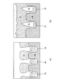
図4は、シートプラズマを湾曲させた場合(傾斜角θは略10°)と、そうさせなかった場合において、基板の配線溝へのCu粒子堆積実験結果の断面写真を模写した図であり、図4(a)は、シートプラズマを湾曲させた場合に相当する図であり、図4(b)は、シートプラズマを湾曲させなかった場合に相当する図である。
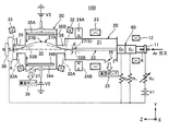
12 第1の電磁コイル
20 シートプラズマ変形室
21 輸送空間
22 円柱プラズマ
23 第2の電磁コイル
24A、24B 棒磁石
25、36 真空ポンプ
26、37 バルブ
27 シートプラズマ
27A 湾曲部
27B 頂点部
28 ボトルネック部
29 通路
30 真空成膜室
31 成膜空間
32 第3の電磁コイル
33 第4の電磁コイル
32A、33A コイル面
32B、33B 法線
34A 基板ホルダ
34B 基板
35A ターゲットホルダ
35B ターゲット
38 永久磁石
40 プラズマガン
50 配線溝
51 Cu堆積膜
52 空孔
100 シートプラズマ成膜装置
A アノード
K カソード
P 輸送中心
S 主面
Claims (5)
- プラズマの輸送方向の中心に対して略等密度分布するソースプラズマを放電により形成して、前記ソースプラズマを前記輸送方向に向けて放出可能なプラズマガンと、
前記輸送方向に延びた輸送空間を有するシートプラズマ変形室と、
互いに同極同士を向き合わせて、前記輸送空間を挟むように配置される第1の磁界発生手段の対と、
前記輸送空間に連通した成膜空間を有する成膜室と、
互いに異極同士を向き合わせて、前記成膜空間を挟むように配置される第2の磁界発生手段の対と、を備え、
前記ソースプラズマは、前記輸送空間を移動する間に、前記第1の磁界発生手段の対の磁界により前記中心を含む主面に沿ってシート状に拡がり、
前記シート状のプラズマは、前記成膜空間を移動する間に、前記第2の磁界発生手段の対の磁界により前記主面から凸状に偏倚するシートプラズマ成膜装置であって、
ターゲットを装着するターゲットホルダと、前記シート状のプラズマ中の荷電粒子により叩き出された前記ターゲットの材料を堆積する基板を装着する基板ホルダと、を更に備え、
前記ターゲットおよび前記基板は、前記シート状のプラズマの厚み方向に間隔を隔て、かつ前記シート状のプラズマを挟むようにして、前記成膜空間内に互いに対向して配置され、
前記シート状のプラズマは、前記主面からターゲットに向かうよう、前記シート状のプラズマの厚み方向に突出した湾曲部を有するシートプラズマ成膜装置。 - 前記第2の磁界発生手段の対は一対の電磁コイルであり、前記電磁コイルのコイル面の法線が、前記主面に対し傾斜している請求項1記載のシートプラズマ成膜装置。
- 前記シート状のプラズマは、略一定の曲率半径により湾曲してなる請求項1記載のシートプラズマ成膜装置。
- 前記電磁コイルの各々のコイル面の法線が、前記ターゲット側に傾斜する、前記主面と所定の傾斜角をなしている請求項2記載のシートプラズマ成膜装置。
- 前記シート状のプラズマの湾曲部は、前記主面から最大に偏倚した頂上部を有し、
前記ターゲットの表面が、前記頂上部に位置するシート状のプラズマ中の荷電粒子に曝されないよう、前記傾斜角の上限が設定されてなる請求項4記載のシートプラズマ成膜装置。
Priority Applications (7)
| Application Number | Priority Date | Filing Date | Title |
|---|---|---|---|
| JP2005351576A JP4906331B2 (ja) | 2005-12-06 | 2005-12-06 | シートプラズマ成膜装置 |
| EP06833564A EP1972700A4 (en) | 2005-12-06 | 2006-11-29 | AREA PLASMA FILM FORMATION DEVICE |
| US12/096,538 US20090314206A1 (en) | 2005-12-06 | 2006-11-29 | Sheet Plasma Film-Forming Apparatus |
| PCT/JP2006/323760 WO2007066548A1 (ja) | 2005-12-06 | 2006-11-29 | シートプラズマ成膜装置 |
| CNA2006800452375A CN101321889A (zh) | 2005-12-06 | 2006-11-29 | 片状等离子体成膜装置 |
| KR1020087011193A KR20080056767A (ko) | 2005-12-06 | 2006-11-29 | 시트 플라즈마 성막장치 |
| TW095144605A TW200745359A (en) | 2005-12-06 | 2006-12-01 | Film-forming apparatus using sheet plasma |
Applications Claiming Priority (1)
| Application Number | Priority Date | Filing Date | Title |
|---|---|---|---|
| JP2005351576A JP4906331B2 (ja) | 2005-12-06 | 2005-12-06 | シートプラズマ成膜装置 |
Publications (2)
| Publication Number | Publication Date |
|---|---|
| JP2007154265A JP2007154265A (ja) | 2007-06-21 |
| JP4906331B2 true JP4906331B2 (ja) | 2012-03-28 |
Family
ID=38122696
Family Applications (1)
| Application Number | Title | Priority Date | Filing Date |
|---|---|---|---|
| JP2005351576A Expired - Fee Related JP4906331B2 (ja) | 2005-12-06 | 2005-12-06 | シートプラズマ成膜装置 |
Country Status (7)
| Country | Link |
|---|---|
| US (1) | US20090314206A1 (ja) |
| EP (1) | EP1972700A4 (ja) |
| JP (1) | JP4906331B2 (ja) |
| KR (1) | KR20080056767A (ja) |
| CN (1) | CN101321889A (ja) |
| TW (1) | TW200745359A (ja) |
| WO (1) | WO2007066548A1 (ja) |
Families Citing this family (11)
| Publication number | Priority date | Publication date | Assignee | Title |
|---|---|---|---|---|
| JP4963992B2 (ja) * | 2007-03-15 | 2012-06-27 | スタンレー電気株式会社 | プラズマ処理装置 |
| JP4934830B2 (ja) * | 2007-11-08 | 2012-05-23 | スタンレー電気株式会社 | プラズマ処理装置 |
| JP4860594B2 (ja) * | 2007-11-28 | 2012-01-25 | 新明和工業株式会社 | スパッタリング装置 |
| JP5231962B2 (ja) * | 2008-12-08 | 2013-07-10 | 新明和工業株式会社 | シートプラズマ成膜装置 |
| JP5498739B2 (ja) * | 2009-08-21 | 2014-05-21 | 新明和工業株式会社 | スパッタリング装置およびスパッタリング方法 |
| JP5374288B2 (ja) * | 2009-09-15 | 2013-12-25 | 新明和工業株式会社 | スパッタリング方法 |
| JP2013522477A (ja) * | 2010-03-22 | 2013-06-13 | アプライド マテリアルズ インコーポレイテッド | 遠隔プラズマ源を用いた誘電体堆積 |
| JP5700695B2 (ja) * | 2012-04-12 | 2015-04-15 | 中外炉工業株式会社 | プラズマ発生装置および蒸着装置並びにプラズマ発生方法 |
| CN102781157B (zh) * | 2012-07-17 | 2014-12-17 | 西安电子科技大学 | 平面射流等离子体产生装置 |
| CN103052249A (zh) * | 2013-01-11 | 2013-04-17 | 哈尔滨工业大学 | 一种射流等离子体密度分布调节器 |
| JP6188224B2 (ja) * | 2013-12-27 | 2017-08-30 | 昭和電工株式会社 | 炭素膜の形成装置、炭素膜の形成方法、及び、磁気記録媒体の製造方法 |
Family Cites Families (11)
| Publication number | Priority date | Publication date | Assignee | Title |
|---|---|---|---|---|
| JPS5927499A (ja) * | 1982-04-12 | 1984-02-13 | 浦本 上進 | 簡単で高能率なシ−トプラズマの生成法 |
| JPS61257471A (ja) * | 1985-05-08 | 1986-11-14 | Joshin Uramoto | 効率的に放電プラズマ流を曲げたイオンプレ−テング装置 |
| DE3880135T2 (de) * | 1988-09-08 | 1993-09-16 | Asahi Glass Co Ltd | Zerstaeubungsverfahren mittels eines bandfoermigen plasmaflusses und geraet zur handhabung dieses verfahrens. |
| JP3095614B2 (ja) * | 1993-04-30 | 2000-10-10 | 株式会社東芝 | 半導体ウェハ等の被処理体をプラズマ処理するに際して使用されるプラズマ処理装置及びプラズマ処理方法 |
| US20020148941A1 (en) * | 1994-02-17 | 2002-10-17 | Boris Sorokov | Sputtering method and apparatus for depositing a coating onto substrate |
| JPH07310186A (ja) * | 1994-05-17 | 1995-11-28 | Nikon Corp | プラズマcvd法および装置 |
| JPH0978230A (ja) * | 1995-09-19 | 1997-03-25 | Chugai Ro Co Ltd | シート状プラズマ発生装置 |
| CN100560787C (zh) * | 2002-02-27 | 2009-11-18 | 亨利J·拉莫斯 | 在磁化的片等离子体源中在金属衬底上形成氮化钛薄膜 |
| JP2003264098A (ja) * | 2002-03-08 | 2003-09-19 | Sumitomo Heavy Ind Ltd | シートプラズマ処理装置 |
| JP2005179767A (ja) * | 2003-12-22 | 2005-07-07 | Joshin Uramoto | スパタイオンプレ−テング装置 |
| JPWO2007066606A1 (ja) * | 2005-12-06 | 2009-05-21 | 新明和工業株式会社 | プラズマ成膜装置 |
-
2005
- 2005-12-06 JP JP2005351576A patent/JP4906331B2/ja not_active Expired - Fee Related
-
2006
- 2006-11-29 CN CNA2006800452375A patent/CN101321889A/zh active Pending
- 2006-11-29 US US12/096,538 patent/US20090314206A1/en not_active Abandoned
- 2006-11-29 EP EP06833564A patent/EP1972700A4/en active Pending
- 2006-11-29 WO PCT/JP2006/323760 patent/WO2007066548A1/ja not_active Ceased
- 2006-11-29 KR KR1020087011193A patent/KR20080056767A/ko not_active Ceased
- 2006-12-01 TW TW095144605A patent/TW200745359A/zh unknown
Also Published As
| Publication number | Publication date |
|---|---|
| TW200745359A (en) | 2007-12-16 |
| EP1972700A1 (en) | 2008-09-24 |
| US20090314206A1 (en) | 2009-12-24 |
| JP2007154265A (ja) | 2007-06-21 |
| EP1972700A4 (en) | 2009-12-09 |
| CN101321889A (zh) | 2008-12-10 |
| WO2007066548A1 (ja) | 2007-06-14 |
| KR20080056767A (ko) | 2008-06-23 |
Similar Documents
| Publication | Publication Date | Title |
|---|---|---|
| US20090071818A1 (en) | Film deposition apparatus and method of film deposition | |
| JP5611039B2 (ja) | スパッタリング装置 | |
| JP4906331B2 (ja) | シートプラズマ成膜装置 | |
| KR20120027033A (ko) | 성막 장치 | |
| US20090159441A1 (en) | Plasma Film Deposition System | |
| US11521822B2 (en) | Ion gun and vacuum processing apparatus | |
| JP2010248576A (ja) | マグネトロンスパッタリング装置 | |
| JP5080977B2 (ja) | シートプラズマ成膜装置 | |
| JP5080294B2 (ja) | イオンガン及び成膜装置 | |
| JP4795174B2 (ja) | スパッタリング装置 | |
| JP6985570B1 (ja) | イオンガン及び真空処理装置 | |
| JP2008053116A (ja) | イオンガン、及び成膜装置 | |
| JP5124317B2 (ja) | シートプラズマ成膜装置、及びシートプラズマ調整方法 | |
| CN117044403B (zh) | 磁控溅射装置用阴极单元及磁控溅射装置 | |
| JP4860594B2 (ja) | スパッタリング装置 | |
| JP5374288B2 (ja) | スパッタリング方法 | |
| JP5118532B2 (ja) | スパッタリング装置およびスパッタリング方法 | |
| JP2009235497A (ja) | スパッタリング装置 | |
| JP5119021B2 (ja) | シートプラズマ成膜装置、及びシートプラズマ調整方法 | |
| JP4854283B2 (ja) | プラズマ成膜方法及びプラズマ成膜装置 | |
| JP2000182525A (ja) | 質量分離型イオン源 | |
| JPS6127463B2 (ja) | ||
| JP2005290442A (ja) | Ecrスパッタリング装置 | |
| KR20150050070A (ko) | 경사진 이온 소스, 이를 갖는 이온빔 처리 장치 및 이온빔 스퍼터링 장치 | |
| JP2010121184A (ja) | スパッタリング装置 |
Legal Events
| Date | Code | Title | Description |
|---|---|---|---|
| A621 | Written request for application examination |
Free format text: JAPANESE INTERMEDIATE CODE: A621 Effective date: 20081029 |
|
| A131 | Notification of reasons for refusal |
Free format text: JAPANESE INTERMEDIATE CODE: A131 Effective date: 20111101 |
|
| A521 | Request for written amendment filed |
Free format text: JAPANESE INTERMEDIATE CODE: A523 Effective date: 20111208 |
|
| TRDD | Decision of grant or rejection written | ||
| A01 | Written decision to grant a patent or to grant a registration (utility model) |
Free format text: JAPANESE INTERMEDIATE CODE: A01 Effective date: 20120110 |
|
| A01 | Written decision to grant a patent or to grant a registration (utility model) |
Free format text: JAPANESE INTERMEDIATE CODE: A01 |
|
| A61 | First payment of annual fees (during grant procedure) |
Free format text: JAPANESE INTERMEDIATE CODE: A61 Effective date: 20120110 |
|
| FPAY | Renewal fee payment (event date is renewal date of database) |
Free format text: PAYMENT UNTIL: 20150120 Year of fee payment: 3 |
|
| R150 | Certificate of patent or registration of utility model |
Free format text: JAPANESE INTERMEDIATE CODE: R150 |
|
| FPAY | Renewal fee payment (event date is renewal date of database) |
Free format text: PAYMENT UNTIL: 20150120 Year of fee payment: 3 |
|
| R250 | Receipt of annual fees |
Free format text: JAPANESE INTERMEDIATE CODE: R250 |
|
| R250 | Receipt of annual fees |
Free format text: JAPANESE INTERMEDIATE CODE: R250 |
|
| LAPS | Cancellation because of no payment of annual fees |