JP4862369B2 - 自発光表示装置、ピーク輝度調整装置、電子機器、ピーク輝度調整方法及びプログラム - Google Patents
自発光表示装置、ピーク輝度調整装置、電子機器、ピーク輝度調整方法及びプログラム Download PDFInfo
- Publication number
- JP4862369B2 JP4862369B2 JP2005340436A JP2005340436A JP4862369B2 JP 4862369 B2 JP4862369 B2 JP 4862369B2 JP 2005340436 A JP2005340436 A JP 2005340436A JP 2005340436 A JP2005340436 A JP 2005340436A JP 4862369 B2 JP4862369 B2 JP 4862369B2
- Authority
- JP
- Japan
- Prior art keywords
- peak luminance
- gradation value
- average gradation
- power consumption
- period
- Prior art date
- Legal status (The legal status is an assumption and is not a legal conclusion. Google has not performed a legal analysis and makes no representation as to the accuracy of the status listed.)
- Expired - Lifetime
Links
Images


Classifications
-
- G—PHYSICS
- G09—EDUCATION; CRYPTOGRAPHY; DISPLAY; ADVERTISING; SEALS
- G09G—ARRANGEMENTS OR CIRCUITS FOR CONTROL OF INDICATING DEVICES USING STATIC MEANS TO PRESENT VARIABLE INFORMATION
- G09G3/00—Control arrangements or circuits, of interest only in connection with visual indicators other than cathode-ray tubes
- G09G3/20—Control arrangements or circuits, of interest only in connection with visual indicators other than cathode-ray tubes for presentation of an assembly of a number of characters, e.g. a page, by composing the assembly by combination of individual elements arranged in a matrix no fixed position being assigned to or needed to be assigned to the individual characters or partial characters
- G09G3/22—Control arrangements or circuits, of interest only in connection with visual indicators other than cathode-ray tubes for presentation of an assembly of a number of characters, e.g. a page, by composing the assembly by combination of individual elements arranged in a matrix no fixed position being assigned to or needed to be assigned to the individual characters or partial characters using controlled light sources
- G09G3/30—Control arrangements or circuits, of interest only in connection with visual indicators other than cathode-ray tubes for presentation of an assembly of a number of characters, e.g. a page, by composing the assembly by combination of individual elements arranged in a matrix no fixed position being assigned to or needed to be assigned to the individual characters or partial characters using controlled light sources using electroluminescent panels
- G09G3/32—Control arrangements or circuits, of interest only in connection with visual indicators other than cathode-ray tubes for presentation of an assembly of a number of characters, e.g. a page, by composing the assembly by combination of individual elements arranged in a matrix no fixed position being assigned to or needed to be assigned to the individual characters or partial characters using controlled light sources using electroluminescent panels semiconductive, e.g. using light-emitting diodes [LED]
- G09G3/3208—Control arrangements or circuits, of interest only in connection with visual indicators other than cathode-ray tubes for presentation of an assembly of a number of characters, e.g. a page, by composing the assembly by combination of individual elements arranged in a matrix no fixed position being assigned to or needed to be assigned to the individual characters or partial characters using controlled light sources using electroluminescent panels semiconductive, e.g. using light-emitting diodes [LED] organic, e.g. using organic light-emitting diodes [OLED]
- G09G3/3225—Control arrangements or circuits, of interest only in connection with visual indicators other than cathode-ray tubes for presentation of an assembly of a number of characters, e.g. a page, by composing the assembly by combination of individual elements arranged in a matrix no fixed position being assigned to or needed to be assigned to the individual characters or partial characters using controlled light sources using electroluminescent panels semiconductive, e.g. using light-emitting diodes [LED] organic, e.g. using organic light-emitting diodes [OLED] using an active matrix
- G09G3/3233—Control arrangements or circuits, of interest only in connection with visual indicators other than cathode-ray tubes for presentation of an assembly of a number of characters, e.g. a page, by composing the assembly by combination of individual elements arranged in a matrix no fixed position being assigned to or needed to be assigned to the individual characters or partial characters using controlled light sources using electroluminescent panels semiconductive, e.g. using light-emitting diodes [LED] organic, e.g. using organic light-emitting diodes [OLED] using an active matrix with pixel circuitry controlling the current through the light-emitting element
-
- G—PHYSICS
- G09—EDUCATION; CRYPTOGRAPHY; DISPLAY; ADVERTISING; SEALS
- G09G—ARRANGEMENTS OR CIRCUITS FOR CONTROL OF INDICATING DEVICES USING STATIC MEANS TO PRESENT VARIABLE INFORMATION
- G09G3/00—Control arrangements or circuits, of interest only in connection with visual indicators other than cathode-ray tubes
- G09G3/20—Control arrangements or circuits, of interest only in connection with visual indicators other than cathode-ray tubes for presentation of an assembly of a number of characters, e.g. a page, by composing the assembly by combination of individual elements arranged in a matrix no fixed position being assigned to or needed to be assigned to the individual characters or partial characters
- G09G3/22—Control arrangements or circuits, of interest only in connection with visual indicators other than cathode-ray tubes for presentation of an assembly of a number of characters, e.g. a page, by composing the assembly by combination of individual elements arranged in a matrix no fixed position being assigned to or needed to be assigned to the individual characters or partial characters using controlled light sources
- G09G3/28—Control arrangements or circuits, of interest only in connection with visual indicators other than cathode-ray tubes for presentation of an assembly of a number of characters, e.g. a page, by composing the assembly by combination of individual elements arranged in a matrix no fixed position being assigned to or needed to be assigned to the individual characters or partial characters using controlled light sources using luminous gas-discharge panels, e.g. plasma panels
- G09G3/288—Control arrangements or circuits, of interest only in connection with visual indicators other than cathode-ray tubes for presentation of an assembly of a number of characters, e.g. a page, by composing the assembly by combination of individual elements arranged in a matrix no fixed position being assigned to or needed to be assigned to the individual characters or partial characters using controlled light sources using luminous gas-discharge panels, e.g. plasma panels using AC panels
- G09G3/291—Control arrangements or circuits, of interest only in connection with visual indicators other than cathode-ray tubes for presentation of an assembly of a number of characters, e.g. a page, by composing the assembly by combination of individual elements arranged in a matrix no fixed position being assigned to or needed to be assigned to the individual characters or partial characters using controlled light sources using luminous gas-discharge panels, e.g. plasma panels using AC panels controlling the gas discharge to control a cell condition, e.g. by means of specific pulse shapes
-
- G—PHYSICS
- G09—EDUCATION; CRYPTOGRAPHY; DISPLAY; ADVERTISING; SEALS
- G09G—ARRANGEMENTS OR CIRCUITS FOR CONTROL OF INDICATING DEVICES USING STATIC MEANS TO PRESENT VARIABLE INFORMATION
- G09G3/00—Control arrangements or circuits, of interest only in connection with visual indicators other than cathode-ray tubes
- G09G3/20—Control arrangements or circuits, of interest only in connection with visual indicators other than cathode-ray tubes for presentation of an assembly of a number of characters, e.g. a page, by composing the assembly by combination of individual elements arranged in a matrix no fixed position being assigned to or needed to be assigned to the individual characters or partial characters
- G09G3/22—Control arrangements or circuits, of interest only in connection with visual indicators other than cathode-ray tubes for presentation of an assembly of a number of characters, e.g. a page, by composing the assembly by combination of individual elements arranged in a matrix no fixed position being assigned to or needed to be assigned to the individual characters or partial characters using controlled light sources
- G09G3/30—Control arrangements or circuits, of interest only in connection with visual indicators other than cathode-ray tubes for presentation of an assembly of a number of characters, e.g. a page, by composing the assembly by combination of individual elements arranged in a matrix no fixed position being assigned to or needed to be assigned to the individual characters or partial characters using controlled light sources using electroluminescent panels
- G09G3/32—Control arrangements or circuits, of interest only in connection with visual indicators other than cathode-ray tubes for presentation of an assembly of a number of characters, e.g. a page, by composing the assembly by combination of individual elements arranged in a matrix no fixed position being assigned to or needed to be assigned to the individual characters or partial characters using controlled light sources using electroluminescent panels semiconductive, e.g. using light-emitting diodes [LED]
-
- G—PHYSICS
- G09—EDUCATION; CRYPTOGRAPHY; DISPLAY; ADVERTISING; SEALS
- G09G—ARRANGEMENTS OR CIRCUITS FOR CONTROL OF INDICATING DEVICES USING STATIC MEANS TO PRESENT VARIABLE INFORMATION
- G09G2300/00—Aspects of the constitution of display devices
- G09G2300/08—Active matrix structure, i.e. with use of active elements, inclusive of non-linear two terminal elements, in the pixels together with light emitting or modulating elements
- G09G2300/0809—Several active elements per pixel in active matrix panels
- G09G2300/0842—Several active elements per pixel in active matrix panels forming a memory circuit, e.g. a dynamic memory with one capacitor
- G09G2300/0861—Several active elements per pixel in active matrix panels forming a memory circuit, e.g. a dynamic memory with one capacitor with additional control of the display period without amending the charge stored in a pixel memory, e.g. by means of additional select electrodes
-
- G—PHYSICS
- G09—EDUCATION; CRYPTOGRAPHY; DISPLAY; ADVERTISING; SEALS
- G09G—ARRANGEMENTS OR CIRCUITS FOR CONTROL OF INDICATING DEVICES USING STATIC MEANS TO PRESENT VARIABLE INFORMATION
- G09G2330/00—Aspects of power supply; Aspects of display protection and defect management
- G09G2330/02—Details of power systems and of start or stop of display operation
- G09G2330/021—Power management, e.g. power saving
-
- G—PHYSICS
- G09—EDUCATION; CRYPTOGRAPHY; DISPLAY; ADVERTISING; SEALS
- G09G—ARRANGEMENTS OR CIRCUITS FOR CONTROL OF INDICATING DEVICES USING STATIC MEANS TO PRESENT VARIABLE INFORMATION
- G09G2330/00—Aspects of power supply; Aspects of display protection and defect management
- G09G2330/02—Details of power systems and of start or stop of display operation
- G09G2330/025—Reduction of instantaneous peaks of current
-
- G—PHYSICS
- G09—EDUCATION; CRYPTOGRAPHY; DISPLAY; ADVERTISING; SEALS
- G09G—ARRANGEMENTS OR CIRCUITS FOR CONTROL OF INDICATING DEVICES USING STATIC MEANS TO PRESENT VARIABLE INFORMATION
- G09G3/00—Control arrangements or circuits, of interest only in connection with visual indicators other than cathode-ray tubes
- G09G3/20—Control arrangements or circuits, of interest only in connection with visual indicators other than cathode-ray tubes for presentation of an assembly of a number of characters, e.g. a page, by composing the assembly by combination of individual elements arranged in a matrix no fixed position being assigned to or needed to be assigned to the individual characters or partial characters
- G09G3/2007—Display of intermediate tones
- G09G3/2014—Display of intermediate tones by modulation of the duration of a single pulse during which the logic level remains constant
Landscapes
- Engineering & Computer Science (AREA)
- Physics & Mathematics (AREA)
- Computer Hardware Design (AREA)
- General Physics & Mathematics (AREA)
- Theoretical Computer Science (AREA)
- Power Engineering (AREA)
- Plasma & Fusion (AREA)
- Control Of Indicators Other Than Cathode Ray Tubes (AREA)
- Electroluminescent Light Sources (AREA)
- Control Of El Displays (AREA)
- Transforming Electric Information Into Light Information (AREA)
Description
なお、発明者らが提案する発明は、自発光表示装置、ピーク輝度調整装置、電子機器、ピーク輝度調整方法及びプログラムとしての側面を有する。
実際、有機ELディスプレイその他の自発光表示装置では、一定輝度のパックライトを常時点灯状態させる方式の表示装置とは異なり、入力される映像信号に応じて表示パネルに流れる電流量が劇的に変化する特性がある。
(a)1フレーム期間中に入力される映像信号の平均階調値を算出する平均階調値算出部
(b)算出された平均階調値に応じた標準ピーク輝度を求め、当該標準ピーク輝度と算出された平均階調値で消費される消費電力量を算出する消費電力算出部
(c)一定期間内に消費される消費電力の合計値が設定電力量を超えないように、標準ピーク輝度を調整するピーク輝度調整部
を実現できる。
なお、本明細書で特に図示又は記載されない部分には、当該技術分野の周知又は公知技術を適用する。
また以下に説明する形態例は、発明の一つの形態例であって、これらに限定されるものではない。
表示パネルのピーク輝度は、最大データの入力時に表示素子に印加される出力電圧(出力電流)又は発光時間の可変制御により調整することができる。
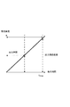
図1に、発光時間と発光輝度との関係を示す。図1に示すように、発光輝度は発光時間に対して線形に変化する。
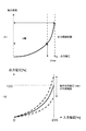
図2(A)に、表示素子に印加される出力電圧と発光輝度との関係を示す。図2(B)に、入力映像信号の階調値(%)と表示素子に印加される出力電圧(基準値を100%で表す。)との間の入出力関係を示す。
従って、発光時間又は最大出力電圧Vmax (最大出力電流Imax )を個別に可変制御すれば、表示パネルのピーク輝度を可変制御することが可能となる。
続いて、ピーク輝度の可変制御を可能とする有機ELパネルモジュールの構造例を説明する。
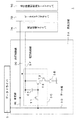
図3に、有機ELパネルモジュール1の構造例を示す。有機ELパネルモジュール1は、発光領域3A(有機EL素子がマトリクス状に配列された領域)と、画像の表示を制御するパネル駆動回路とで構成される。
パネル駆動回路は、データドライバ5、最大出力電圧制御用ドライバ7A、ゲートスキャンドライバ7B、点灯時間制御用ゲートドライバ7Cで構成される。なお、パネル駆動回路は、発光領域3Aの周辺部に形成する。
このうち、データスイッチ素子T1は、データ線3Dを通じて与えられる電圧値の取り込みタイミングを制御するのに用いられる。取り込みタイミングは、走査線3Eを通じて線順次で与えられる。
電流駆動素子T2は、キャパシタC1の電圧値に応じた電流を有機EL素子3Bに供給するのに用いられる。駆動電流は、電流供給線3Fを通じて供給される。なお、この電流供給線3Fには、最大出力電圧制御用ドライバ7Aを通じて最大出力電圧Vmax が印加される。
この点灯スイッチ素子T3の開閉動作を制御するデューティパルス(図4(B))を供給するのが点灯制御線3Gである。なお、図4(A)は、基準期間としての1フレーム期間を示す。
なお、ピーク輝度を発光時間長で制御する場合には、最大出力電圧制御用ドライバ7Aは全てのフレームについて固定電圧を供給する。一方、ピーク輝度を最大出力電圧Vmax で制御する場合には、点灯時間制御用ゲートドライバ7Cは、全てのフレームについて固定比のデューティパルスを供給する。
なお、発光領域3Aの周辺回路(パネル駆動回路)は、半導体集積回路としてパネル基板上に搭載しても良いし、パネル基板上に半導体プロセスを用いて直接形成しても良い。
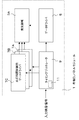
以下、一定期間内に消費される消費電力の合計値が設定電力量を超えないように、映像信号のピーク輝度をリアルタイムで制御可能なピーク輝度調整装置11(図6)の形態例を説明する。
図6に、ピーク輝度調整装置11に採用して好適な構成例の一つを示す。
この形態例に係るピーク輝度調整装置11は、平均階調値算出部13と、消費電力量一定化制御部15と、ピーク輝度制御部17と、フレーム遅延部19とで構成する。
平均階調値算出部13は、1フレーム期間中に入力される映像信号の平均階調値APLn をフレーム単位で算出する処理デバイスである。ここでの添字nは、時間(例えばフレーム番号)を意味する。
グレースケール変換部131は、入力された映像信号をグレースケール信号に変換する処理デバイスである。
1フレーム内全画素階調平均計算部133は、1フレームを構成する全画素について階調値の平均値を算出する処理デバイスである。
図8に、消費電力量一定化制御部15の内部構成例を示す。消費電力量一定化制御部15は、消費電力算出部151と、ピーク輝度調整部153で構成する。
消費電力算出部151は、算出された平均階調値APLに応じた標準ピーク輝度を読み出し、当該標準ピーク輝度と算出された平均階調値で消費される消費電力量を算出する処理デバイスである。
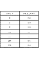
この場合、あるフレームの消費電力は、平均階調値APL×ピーク輝度倍率SEL_PK×基準ピーク輝度で与えられる。
消費電力算出部151は、平均階調値APLに応じたピーク輝度倍率SEL_PKを、図9に示すルックアップテーブルを使用して読み出す。
一方、図9に示すルックアップテーブルでは、平均階調値APLが大きいほど、ピーク輝度倍率SEL_PKを小さな値に設定する。
平均階調値APLに応じたピーク輝度倍率SEL_PKを以上の関係に定めることにより、画質を考慮した標準ピーク輝度が得られる。
ピーク輝度調整部153は、基準期間(制御単位)内の残存期間で消費可能な実際の消費電力量(残存電力量)Aと、基準期間(制御単位)の全期間を同じピーク輝度で常時点灯する場合における残存期間での消費電力量Bとの比に応じて、対応フレームのピーク輝度を調整する。
ここで、実際の残存電力量Aは、(Sn-1
−APLn ×SEL_PKn )×基準ピーク輝度で与える。また、同一ピーク輝度で常時点灯する場合に消費可能な残存電力量Bは、((Tflat−n)×APLflat)×基準ピーク輝度で与える。
なお、Tflatは、基準期間に設定したフレーム数である。また、APLflatは、消費電力量を制限するためのAPL設定値(規定された消費電力を満たすように、基準期間の全期間を同じピーク輝度で点灯する場合におけるフレーム単位の平均階調値)である。
また、nフレーム目をピーク輝度倍率PKn で点灯した場合における残存電力量A(=Sn )は、n−1フレーム目の残存電力量Sn-1 を用いることにより、Sn-1 −APLn ×PKn で与えられる。なお、計算上は基準ピーク輝度が省略されるため、ここでの電力量では、乗算すべき基準ピーク輝度の記載を省略している。
例えば、設定された消費電力を達成する平均階調値よりも明るいフレームが続く等により、実際の残存消費電力Aが全期間を平均的に点灯制御する際の残存電力量Bよりも小さくなっている場合には、調整後のピーク輝度倍率PKn は、本来の平均階調値に対応するピーク輝度倍率SEL_PKn よりも小さい値に制御される。
なお、ピーク輝度制御部17は、入力映像信号の垂直同期信号Vsyncに同期したタイミングでピークコントロール信号を生成する。
図10に、入出力フレームの位相関係を示す。図10(A)は、映像信号VSのフレーム番号(位相)を示す図である。図10(B)は、フレーム遅延部19に入力される画像データの番号(位相)を示す図である。
図10(B)及び(D)を対比して分かるように、フレーム遅延部19では画像データが1フレーム分遅延されている。このため、図10(D)及び(E)に示すように、映像信号とピークコントロール信号の同期が確保される。
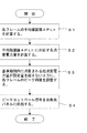
図11に、以上説明したピーク輝度調整装置11で実行される処理動作の概略を示す。
ピーク輝度調整装置11は、各フレームの平均階調値APLn を算出し(S1)、平均階調値に対応するピーク輝度倍率SEL_PKを求める。
この後、ピーク輝度調整装置11は、現フレームの平均階調値APLn とピーク輝度倍率SEL_PKとを用いて入力映像信号本来の消費電力量を算出する(S2)。
調整後のピーク輝度(倍率)に応じてパルス幅変調したピークコントロール信号を有機ELパネルモジュール1に出力する(S4)。
いずれの基準期間(0−t0 、t1 −t2 、t2 −t3 …)についても、各基準期間で消費可能な設定電力量Smax 以下に抑制されていることが分かる。
なお、Sn (n=0、1、2…)は、各基準期間内での実際の消費電力量である。
以上説明したピーク輝度調整装置をパネル基板上に搭載することにより、有機ELパネルの定消費電力化又は消費電力抑制化を実現できる。勿論、入力映像信号に応じたピーク輝度で点灯制御しても事前に設定した消費電力量を満たす場合には、入力映像信号を高い画質のまま表示することができる。
また、前述したピーク輝度の可変調整機能は、ソフトウェア処理で実現する場合にも演算負荷が小さく、集積回路で実現する場合にも非常に小規模な回路で実現することが可能であり、有機ELパネルモジュールへの実装に有利である。
(a)前述の形態例では、発光時間の調整によりピーク輝度を可変制御する場合について説明したが、最大出力電圧の調整によりピーク輝度を可変制御しても良い。また、発光時間及び最大出力電圧の双方を同時に調整し、ピーク輝度を可変制御しても良い。
(b)前述の形態例では、算出された平均階調値APLに対応する標準ピーク輝度SEL_PKを、ルックアップテーブルから読み出す場合について説明したが、事前に設定した関係に従って算出しても良い。
しかし、ピーク輝度の可変制御機能は、発光時間又は最大出力電圧のいずれか一方を可変制御することで実現できる。従って、発光時間を可変制御する方式を採用する場合には最大出力電圧制御用ドライバ7Aを搭載しない構成を採用し、最大出力電圧を可変制御する方式を採用する場合には点灯時間制御用ゲートドライバ7Cを搭載しない構成を採用しても良い。
Panel)パネルその他の自発光パネルに適用できる。
しかし、この有機ELディスプレイパネルその他の表示装置は、単独の商品形態でも良いし、他の画像処理装置の一部として搭載されても良い。
例えば、ビデオカメラ、デジタルカメラその他の撮像装置(カメラユニットだけでなく、記録装置と一体に構成されているものを含む。)、情報処理端末(携帯型のコンピュータ、携帯電話機、携帯型のゲーム機、電子手帳等)、ゲーム機の表示デバイスとしも実現できる。
特に、バッテリー駆動される電子機器に搭載する場合には、既存のバッテリー容量でより長時間の使用を達成できる。
しかし、ピーク輝度調整装置11は、有機ELディスプレイパネルその他の表示装置に対して入力映像信号を供給する画像処理装置側に搭載しても良い。この場合、画像処理装置から表示装置にデューティパルスや電圧値を供給する方式を採用しても良いし、これらの値を指示する情報を画像処理装置から表示装置に与える方式を採用しても良い。
また、これらの処理機能の全てをハードウェア又はソフトウェアで実現するだけでなく、その一部はハードウェア又はソフトウェアを用いて実現しても良い。すなわち、ハードウェアとソフトウェアの組み合わせ構成としても良い。
(h)前述の形態例には、発明の趣旨の範囲内で様々な変形例が考えられる。また、本明細書の記載に基づいて創作される又は組み合わせられる各種の変形例及び応用例も考えられる。
3A 発光領域
5 データドライバ
7A 電圧切替ドライバ7A
7B ゲートスキャンドライバ
7C 点灯時間制御用ゲートドライバ
9 タイミングジェネレータ
11 ピーク輝度調整装置
13 平均階調値算出部
15 消費電力量一定化制御部
151 消費電力算出部
153 ピーク輝度調整部
17 ピーク輝度制御部
19 フレーム遅延部
Claims (6)
- 自発光パネル面のピーク輝度を1フレーム単位で可変制御可能な自発光表示装置において、
1フレーム期間中に入力される映像信号の平均階調値を算出する平均階調値算出部と、
算出された平均階調値に応じて、平均階調値との間に所定の負の相関がある標準ピーク輝度を求め、当該標準ピーク輝度と算出された平均階調値で消費される消費電力量を算出する消費電力算出部と、
一定期間内に消費される消費電力の合計値が設定電力量を超えないように、前記標準ピーク輝度を調整するピーク輝度調整部とを有しており、
前記ピーク輝度調整部は、調整後の標準ピーク輝度を、(A/B)×標準ピーク輝度で与える自発光表示装置。
ただし、Aは、制御単位に定めた一定期間内での残存期間に消費可能な実際の消費電力量であり、Bは、制御単位に定めた一定期間の全期間を同じピーク輝度で点灯する場合に残存期間に消費可能な消費電力量である。 - 請求項1に記載の自発光表示装置において、
算出された平均階調値に応じた標準ピーク輝度は、個々の平均階調値と標準ピーク輝度の組み合わせを記録した対応テーブルより読み出される自発光表示装置。 - 自発光パネル面のピーク輝度を1フレーム単位で調整するピーク輝度調整装置において、
1フレーム期間中に入力される映像信号の平均階調値を算出する平均階調値算出部と、
算出された平均階調値に応じて、平均階調値との間に所定の負の相関がある標準ピーク輝度を求め、当該標準ピーク輝度と算出された平均階調値で消費される消費電力量を算出する消費電力算出部と、
一定期間内に消費される消費電力の合計値が設定電力量を超えないように、前記標準ピーク輝度を調整するピーク輝度調整部とを有しており、
前記ピーク輝度調整部は、調整後の標準ピーク輝度を、(A/B)×標準ピーク輝度で与えるピーク輝度調整装置。
ただし、Aは、制御単位に定めた一定期間内での残存期間に消費可能な実際の消費電力量であり、Bは、制御単位に定めた一定期間の全期間を同じピーク輝度で点灯する場合に残存期間に消費可能な消費電力量である。 - 自発光パネル面のピーク輝度を1フレーム単位で調整するピーク輝度調整装置を搭載する電子機器において、
1フレーム期間中に入力される映像信号の平均階調値を算出する平均階調値算出部と、
算出された平均階調値に応じて、平均階調値との間に所定の負の相関がある標準ピーク輝度を求め、当該標準ピーク輝度と算出された平均階調値で消費される消費電力量を算出する消費電力算出部と、
一定期間内に消費される消費電力の合計値が設定電力量を超えないように、前記標準ピーク輝度を調整するピーク輝度調整部とを有しており、
前記ピーク輝度調整部は、調整後の標準ピーク輝度を、(A/B)×標準ピーク輝度で与える電子機器。
ただし、Aは、制御単位に定めた一定期間内での残存期間に消費可能な実際の消費電力量であり、Bは、制御単位に定めた一定期間の全期間を同じピーク輝度で点灯する場合に残存期間に消費可能な消費電力量である。 - 自発光パネル面のピーク輝度を1フレーム単位で調整するピーク輝度調整方法において、
1フレーム期間中に入力される映像信号の平均階調値を算出する処理と、
算出された平均階調値に応じて、平均階調値との間に所定の負の相関がある標準ピーク輝度を求め、当該標準ピーク輝度と算出された平均階調値で消費される消費電力量を算出する処理と、
一定期間内に消費される消費電力の合計値が設定電力量を超えないように、前記標準ピーク輝度を調整する処理と
を有しており、
前記標準ピーク輝度を調整する処理は、調整後の標準ピーク輝度を、(A/B)×標準ピーク輝度で与えるピーク輝度調整方法。
ただし、Aは、制御単位に定めた一定期間内での残存期間に消費可能な実際の消費電力量であり、Bは、制御単位に定めた一定期間の全期間を同じピーク輝度で点灯する場合に残存期間に消費可能な消費電力量である。 - 自発光パネル面のピーク輝度を1フレーム単位で調整するコンピュータに、
1フレーム期間中に入力される映像信号の平均階調値を算出する処理と、
算出された平均階調値に応じて、平均階調値との間に所定の負の相関がある標準ピーク輝度を求め、当該標準ピーク輝度と算出された平均階調値で消費される消費電力量を算出する処理と、
一定期間内に消費される消費電力の合計値が設定電力量を超えないように、前記標準ピーク輝度を調整する処理とを実行させるコンピュータプログラムにおいて、
前記標準ピーク輝度を調整する処理は、調整後の標準ピーク輝度を、(A/B)×標準ピーク輝度で与えるコンピュータプログラム。
ただし、Aは、制御単位に定めた一定期間内での残存期間に消費可能な実際の消費電力量であり、Bは、制御単位に定めた一定期間の全期間を同じピーク輝度で点灯する場合に残存期間に消費可能な消費電力量である。
Priority Applications (6)
| Application Number | Priority Date | Filing Date | Title |
|---|---|---|---|
| JP2005340436A JP4862369B2 (ja) | 2005-11-25 | 2005-11-25 | 自発光表示装置、ピーク輝度調整装置、電子機器、ピーク輝度調整方法及びプログラム |
| TW095143031A TW200733045A (en) | 2005-11-25 | 2006-11-21 | Self light-emitting display apparatus, peak brightness adjustment apparatus, electronic machine, peak brightness adjustment method and program |
| US11/603,215 US8325115B2 (en) | 2005-11-25 | 2006-11-22 | Self-luminous display apparatus, peak luminance adjustment apparatus, electronic apparatus, peak luminance adjustment method and program |
| KR1020060116312A KR101367916B1 (ko) | 2005-11-25 | 2006-11-23 | 자발광 표시장치, 피크 휘도 조정 장치, 전자기기, 피크휘도 조정 방법 및 프로그램 |
| CNB2006100644574A CN100524399C (zh) | 2005-11-25 | 2006-11-24 | 显示装置、电子装置、峰值亮度调整装置及方法 |
| US13/657,388 US9214108B2 (en) | 2005-11-25 | 2012-10-22 | Self-luminous display apparatus, peak luminance adjustment apparatus, electronic apparatus, peak luminance adjustment method and program |
Applications Claiming Priority (1)
| Application Number | Priority Date | Filing Date | Title |
|---|---|---|---|
| JP2005340436A JP4862369B2 (ja) | 2005-11-25 | 2005-11-25 | 自発光表示装置、ピーク輝度調整装置、電子機器、ピーク輝度調整方法及びプログラム |
Publications (2)
| Publication Number | Publication Date |
|---|---|
| JP2007147868A JP2007147868A (ja) | 2007-06-14 |
| JP4862369B2 true JP4862369B2 (ja) | 2012-01-25 |
Family
ID=38118179
Family Applications (1)
| Application Number | Title | Priority Date | Filing Date |
|---|---|---|---|
| JP2005340436A Expired - Lifetime JP4862369B2 (ja) | 2005-11-25 | 2005-11-25 | 自発光表示装置、ピーク輝度調整装置、電子機器、ピーク輝度調整方法及びプログラム |
Country Status (5)
| Country | Link |
|---|---|
| US (2) | US8325115B2 (ja) |
| JP (1) | JP4862369B2 (ja) |
| KR (1) | KR101367916B1 (ja) |
| CN (1) | CN100524399C (ja) |
| TW (1) | TW200733045A (ja) |
Families Citing this family (68)
| Publication number | Priority date | Publication date | Assignee | Title |
|---|---|---|---|---|
| CA2443206A1 (en) | 2003-09-23 | 2005-03-23 | Ignis Innovation Inc. | Amoled display backplanes - pixel driver circuits, array architecture, and external compensation |
| US9799246B2 (en) | 2011-05-20 | 2017-10-24 | Ignis Innovation Inc. | System and methods for extraction of threshold and mobility parameters in AMOLED displays |
| US8576217B2 (en) | 2011-05-20 | 2013-11-05 | Ignis Innovation Inc. | System and methods for extraction of threshold and mobility parameters in AMOLED displays |
| WO2006063448A1 (en) | 2004-12-15 | 2006-06-22 | Ignis Innovation Inc. | Method and system for programming, calibrating and driving a light emitting device display |
| US20140111567A1 (en) * | 2005-04-12 | 2014-04-24 | Ignis Innovation Inc. | System and method for compensation of non-uniformities in light emitting device displays |
| US10012678B2 (en) | 2004-12-15 | 2018-07-03 | Ignis Innovation Inc. | Method and system for programming, calibrating and/or compensating, and driving an LED display |
| US10013907B2 (en) * | 2004-12-15 | 2018-07-03 | Ignis Innovation Inc. | Method and system for programming, calibrating and/or compensating, and driving an LED display |
| US7852298B2 (en) | 2005-06-08 | 2010-12-14 | Ignis Innovation Inc. | Method and system for driving a light emitting device display |
| US8477121B2 (en) | 2006-04-19 | 2013-07-02 | Ignis Innovation, Inc. | Stable driving scheme for active matrix displays |
| JP2007322718A (ja) * | 2006-05-31 | 2007-12-13 | Sanyo Electric Co Ltd | 表示装置 |
| CA2556961A1 (en) | 2006-08-15 | 2008-02-15 | Ignis Innovation Inc. | Oled compensation technique based on oled capacitance |
| JP2008252185A (ja) * | 2007-03-29 | 2008-10-16 | Kyocera Corp | 携帯電子機器 |
| JP5034805B2 (ja) * | 2007-09-13 | 2012-09-26 | ソニー株式会社 | 表示装置、表示駆動方法 |
| JP5176522B2 (ja) * | 2007-12-13 | 2013-04-03 | ソニー株式会社 | 自発光型表示装置およびその駆動方法 |
| JP5211732B2 (ja) * | 2008-02-14 | 2013-06-12 | ソニー株式会社 | 点灯期間設定方法、表示パネルの駆動方法、点灯条件設定装置、半導体デバイス、表示パネル及び電子機器 |
| JP5091796B2 (ja) * | 2008-08-05 | 2012-12-05 | 株式会社東芝 | 画像処理装置 |
| CN102203847B (zh) * | 2008-10-10 | 2013-08-21 | 夏普株式会社 | 图像显示用发光装置的功率控制方法、图像显示用发光装置、显示装置和电视接收装置 |
| JP5321032B2 (ja) * | 2008-12-11 | 2013-10-23 | ソニー株式会社 | 表示装置、輝度調整装置、輝度調整方法及びプログラム |
| JP5304211B2 (ja) | 2008-12-11 | 2013-10-02 | ソニー株式会社 | 表示装置、輝度調整装置、バックライト装置、輝度調整方法及びプログラム |
| US9384698B2 (en) | 2009-11-30 | 2016-07-05 | Ignis Innovation Inc. | System and methods for aging compensation in AMOLED displays |
| JP2011002520A (ja) * | 2009-06-16 | 2011-01-06 | Sony Corp | 自発光表示装置、消費電力削減方法及びプログラム |
| CA2669367A1 (en) | 2009-06-16 | 2010-12-16 | Ignis Innovation Inc | Compensation technique for color shift in displays |
| US10319307B2 (en) | 2009-06-16 | 2019-06-11 | Ignis Innovation Inc. | Display system with compensation techniques and/or shared level resources |
| US9311859B2 (en) | 2009-11-30 | 2016-04-12 | Ignis Innovation Inc. | Resetting cycle for aging compensation in AMOLED displays |
| KR101658138B1 (ko) * | 2009-10-07 | 2016-09-21 | 엘지디스플레이 주식회사 | 유기 발광 다이오드 표시장치의 구동장치와 그 구동방법 |
| US20140313111A1 (en) | 2010-02-04 | 2014-10-23 | Ignis Innovation Inc. | System and methods for extracting correlation curves for an organic light emitting device |
| US9881532B2 (en) | 2010-02-04 | 2018-01-30 | Ignis Innovation Inc. | System and method for extracting correlation curves for an organic light emitting device |
| CA2692097A1 (en) | 2010-02-04 | 2011-08-04 | Ignis Innovation Inc. | Extracting correlation curves for light emitting device |
| US10089921B2 (en) | 2010-02-04 | 2018-10-02 | Ignis Innovation Inc. | System and methods for extracting correlation curves for an organic light emitting device |
| US8907991B2 (en) | 2010-12-02 | 2014-12-09 | Ignis Innovation Inc. | System and methods for thermal compensation in AMOLED displays |
| US9530349B2 (en) | 2011-05-20 | 2016-12-27 | Ignis Innovations Inc. | Charged-based compensation and parameter extraction in AMOLED displays |
| US9466240B2 (en) | 2011-05-26 | 2016-10-11 | Ignis Innovation Inc. | Adaptive feedback system for compensating for aging pixel areas with enhanced estimation speed |
| CN106910464B (zh) | 2011-05-27 | 2020-04-24 | 伊格尼斯创新公司 | 补偿显示器阵列中像素的系统和驱动发光器件的像素电路 |
| KR101492682B1 (ko) * | 2011-09-23 | 2015-02-13 | 엘지디스플레이 주식회사 | 유기전계발광표시장치와 이의 구동방법 |
| US10089924B2 (en) | 2011-11-29 | 2018-10-02 | Ignis Innovation Inc. | Structural and low-frequency non-uniformity compensation |
| US9324268B2 (en) | 2013-03-15 | 2016-04-26 | Ignis Innovation Inc. | Amoled displays with multiple readout circuits |
| US8937632B2 (en) | 2012-02-03 | 2015-01-20 | Ignis Innovation Inc. | Driving system for active-matrix displays |
| JP2013228560A (ja) * | 2012-04-25 | 2013-11-07 | Sharp Corp | 発光ダイオード制御回路および表示装置 |
| US8922544B2 (en) | 2012-05-23 | 2014-12-30 | Ignis Innovation Inc. | Display systems with compensation for line propagation delay |
| KR101937937B1 (ko) * | 2012-10-12 | 2019-04-11 | 엘지디스플레이 주식회사 | 피크휘도제어부 및 이를 포함하는 유기발광다이오드 표시장치 |
| KR101456958B1 (ko) * | 2012-10-15 | 2014-10-31 | 엘지디스플레이 주식회사 | 유기 발광 표시 장치의 구동 장치 및 구동 방법 |
| KR101992904B1 (ko) * | 2012-12-21 | 2019-06-26 | 엘지디스플레이 주식회사 | Oled 표시 장치 및 그의 구동 방법 |
| JP5957675B2 (ja) | 2012-12-21 | 2016-07-27 | 株式会社Joled | 自発光表示装置、自発光表示装置の制御方法及びコンピュータプログラム |
| EP2779147B1 (en) | 2013-03-14 | 2016-03-02 | Ignis Innovation Inc. | Re-interpolation with edge detection for extracting an aging pattern for AMOLED displays |
| US9368067B2 (en) | 2013-05-14 | 2016-06-14 | Apple Inc. | Organic light-emitting diode display with dynamic power supply control |
| JP6274771B2 (ja) * | 2013-07-26 | 2018-02-07 | 株式会社ジャパンディスプレイ | 発光素子表示装置 |
| KR102074719B1 (ko) | 2013-10-08 | 2020-02-07 | 엘지디스플레이 주식회사 | 유기 발광 표시 장치 |
| CN103531155B (zh) * | 2013-10-09 | 2016-01-20 | 广东欧珀移动通信有限公司 | 带录像功能的移动设备在录像时降低功耗的方法及装置 |
| US9396684B2 (en) | 2013-11-06 | 2016-07-19 | Apple Inc. | Display with peak luminance control sensitive to brightness setting |
| CN104332151B (zh) * | 2013-11-06 | 2017-04-12 | 苹果公司 | 显示器、显示器电路和操作显示器的方法 |
| JP2015099181A (ja) * | 2013-11-18 | 2015-05-28 | 株式会社ジャパンディスプレイ | 表示装置 |
| US9761170B2 (en) | 2013-12-06 | 2017-09-12 | Ignis Innovation Inc. | Correction for localized phenomena in an image array |
| US9741282B2 (en) | 2013-12-06 | 2017-08-22 | Ignis Innovation Inc. | OLED display system and method |
| US9502653B2 (en) | 2013-12-25 | 2016-11-22 | Ignis Innovation Inc. | Electrode contacts |
| US10192479B2 (en) | 2014-04-08 | 2019-01-29 | Ignis Innovation Inc. | Display system using system level resources to calculate compensation parameters for a display module in a portable device |
| JP6343515B2 (ja) | 2014-07-31 | 2018-06-13 | 株式会社ジャパンディスプレイ | 表示装置 |
| KR102242761B1 (ko) * | 2014-10-23 | 2021-04-21 | 엘지디스플레이 주식회사 | 데이터 변환 장치 및 이를 이용한 디스플레이 장치 |
| CA2879462A1 (en) | 2015-01-23 | 2016-07-23 | Ignis Innovation Inc. | Compensation for color variation in emissive devices |
| CA2889870A1 (en) | 2015-05-04 | 2016-11-04 | Ignis Innovation Inc. | Optical feedback system |
| CA2892714A1 (en) | 2015-05-27 | 2016-11-27 | Ignis Innovation Inc | Memory bandwidth reduction in compensation system |
| KR102473208B1 (ko) * | 2015-07-06 | 2022-12-05 | 삼성디스플레이 주식회사 | 유기전계발광 표시장치 및 그의 구동 방법 |
| CA2900170A1 (en) | 2015-08-07 | 2017-02-07 | Gholamreza Chaji | Calibration of pixel based on improved reference values |
| JP2017076007A (ja) * | 2015-10-13 | 2017-04-20 | 株式会社ジャパンディスプレイ | 制御装置及び表示装置 |
| KR20170049735A (ko) | 2015-10-28 | 2017-05-11 | 삼성디스플레이 주식회사 | 표시 장치 |
| KR101884233B1 (ko) * | 2016-08-26 | 2018-08-01 | 삼성전자주식회사 | 디스플레이 장치 및 그 구동 방법 |
| US10181278B2 (en) | 2016-09-06 | 2019-01-15 | Microsoft Technology Licensing, Llc | Display diode relative age |
| JP2019168501A (ja) * | 2018-03-22 | 2019-10-03 | キヤノン株式会社 | 表示制御装置および表示制御方法 |
| CN118366413B (zh) * | 2024-06-20 | 2024-09-13 | 深圳市阿龙电子有限公司 | 一种智能手表的显示功耗控制方法及系统 |
Family Cites Families (23)
| Publication number | Priority date | Publication date | Assignee | Title |
|---|---|---|---|---|
| JP2994630B2 (ja) * | 1997-12-10 | 1999-12-27 | 松下電器産業株式会社 | 明るさによるサブフィールド数調整可能な表示装置 |
| JP3544855B2 (ja) * | 1998-03-26 | 2004-07-21 | 富士通株式会社 | 表示ユニットの消費電力制御方法と装置、その装置を含む表示システム、及びその方法を実現するプログラムを格納した記憶媒体 |
| WO2000017845A1 (en) * | 1998-09-18 | 2000-03-30 | Matsushita Electric Industrial Co., Ltd. | Colour display apparatus |
| JP3242641B1 (ja) * | 1998-09-18 | 2001-12-25 | 松下電器産業株式会社 | プラズマ表示装置 |
| JP3811738B2 (ja) * | 1998-12-24 | 2006-08-23 | 株式会社日立プラズマパテントライセンシング | 表示装置 |
| JP2000276091A (ja) * | 1999-03-24 | 2000-10-06 | Canon Inc | フラットパネル型表示装置及びフラットパネル型表示装置の制御方法 |
| JP2001343941A (ja) | 2000-05-30 | 2001-12-14 | Hitachi Ltd | 表示装置 |
| JP2001346219A (ja) * | 2000-05-31 | 2001-12-14 | Fujitsu General Ltd | プロジェクション方法及びプロジェクタ装置 |
| JP2002132218A (ja) | 2000-10-26 | 2002-05-09 | Sony Corp | 表示装置、輝度制限回路及び表示装置の駆動方法 |
| JP2003015605A (ja) | 2001-07-03 | 2003-01-17 | Sony Corp | アクティブマトリクス型表示装置およびアクティブマトリクス型有機エレクトロルミネッセンス表示装置、並びにそれらの駆動方法 |
| US7030956B2 (en) * | 2002-03-11 | 2006-04-18 | Sony Corporation | Optical intensity modulation method and system, and optical state modulation apparatus |
| JP3922090B2 (ja) * | 2002-05-17 | 2007-05-30 | 株式会社日立製作所 | 表示装置及び表示制御方法 |
| JP3674606B2 (ja) * | 2002-06-11 | 2005-07-20 | ソニー株式会社 | 光量変調装置、表示システム及び光量変調方法 |
| US20050062696A1 (en) * | 2003-09-24 | 2005-03-24 | Shin-Tai Lo | Driving apparatus and method of a display device for automatically adjusting the optimum brightness under limited power consumption |
| US20050123193A1 (en) * | 2003-12-05 | 2005-06-09 | Nokia Corporation | Image adjustment with tone rendering curve |
| JP4519493B2 (ja) * | 2004-03-25 | 2010-08-04 | パナソニック株式会社 | 表示装置 |
| EP1622119A1 (en) * | 2004-07-29 | 2006-02-01 | Deutsche Thomson-Brandt Gmbh | Method and apparatus for power level control and/or contrast control of a display device |
| WO2006025359A1 (ja) * | 2004-09-03 | 2006-03-09 | Sharp Kabushiki Kaisha | 表示装置の駆動方法、表示装置の駆動装置、そのプログラムおよび記録媒体、並びに、表示装置 |
| JP4403401B2 (ja) * | 2004-10-13 | 2010-01-27 | ソニー株式会社 | 情報処理装置および方法、記録媒体、並びにプログラム |
| US7880815B2 (en) * | 2005-01-10 | 2011-02-01 | Mavs Lab, Inc. | Method for detecting and eliminating flash scene in digital video |
| JP2006201399A (ja) * | 2005-01-19 | 2006-08-03 | Fuji Photo Film Co Ltd | 表示装置及び表示制御方法 |
| US7236845B2 (en) * | 2005-03-10 | 2007-06-26 | Eastman Kodak Company | Selecting OLED devices using figure of merit |
| US8847972B2 (en) * | 2010-01-20 | 2014-09-30 | Intellectual Ventures Fund 83 Llc | Adapting display color for low luminance conditions |
-
2005
- 2005-11-25 JP JP2005340436A patent/JP4862369B2/ja not_active Expired - Lifetime
-
2006
- 2006-11-21 TW TW095143031A patent/TW200733045A/zh unknown
- 2006-11-22 US US11/603,215 patent/US8325115B2/en active Active
- 2006-11-23 KR KR1020060116312A patent/KR101367916B1/ko active Active
- 2006-11-24 CN CNB2006100644574A patent/CN100524399C/zh active Active
-
2012
- 2012-10-22 US US13/657,388 patent/US9214108B2/en active Active
Also Published As
| Publication number | Publication date |
|---|---|
| JP2007147868A (ja) | 2007-06-14 |
| US20070126672A1 (en) | 2007-06-07 |
| CN100524399C (zh) | 2009-08-05 |
| TW200733045A (en) | 2007-09-01 |
| US9214108B2 (en) | 2015-12-15 |
| KR101367916B1 (ko) | 2014-02-27 |
| US20130050295A1 (en) | 2013-02-28 |
| KR20070055374A (ko) | 2007-05-30 |
| TWI357050B (ja) | 2012-01-21 |
| US8325115B2 (en) | 2012-12-04 |
| CN101030346A (zh) | 2007-09-05 |
Similar Documents
| Publication | Publication Date | Title |
|---|---|---|
| JP4862369B2 (ja) | 自発光表示装置、ピーク輝度調整装置、電子機器、ピーク輝度調整方法及びプログラム | |
| JP4036142B2 (ja) | 電気光学装置、電気光学装置の駆動方法および電子機器 | |
| KR101425889B1 (ko) | 피크 강도 레벨 제어장치, 자체 발광 표시장치, 전자기기,피크 강도 레벨 제어방법 및 컴퓨터 프로그램 | |
| CN101630906B (zh) | 具有pwm与pfm自动切换的直流对直流变压器及oled显示器 | |
| JP2008026395A (ja) | 消費電力検出装置、消費電力制御装置、画像処理装置、自発光表示装置、電子機器、消費電力検出方法、消費電力制御方法及びコンピュータプログラム | |
| JP2008026761A (ja) | 消費電力制御装置、画像処理装置、自発光表示装置、電子機器、消費電力制御方法及びコンピュータプログラム | |
| KR100782456B1 (ko) | 유기 전계발광 표시장치의 구동 방법 | |
| JP4952972B2 (ja) | 自発光表示装置、発光条件最適化装置、発光条件最適化方法及びプログラム | |
| JP4899447B2 (ja) | 自発光表示装置、発光条件制御装置、発光条件制御方法及びプログラム | |
| JP5082319B2 (ja) | 発光条件制御装置、画像処理装置、自発光表示装置、電子機器、発光条件制御方法及びコンピュータプログラム | |
| JP2007164003A (ja) | 自発光表示装置、画像処理装置、点灯時間長制御装置及びプログラム | |
| JP2007147867A (ja) | 自発光表示装置、発光条件制御装置、発光条件制御方法及びプログラム | |
| JP2008292866A (ja) | カソード電位制御装置、自発光表示装置、電子機器及びカソード電位制御方法 | |
| JP2008292867A (ja) | コントラスト制御装置、自発光表示装置、電子機器及びコントラスト制御方法 | |
| JP2006284974A (ja) | 面内温度調整方法、表示装置、面内温度調整装置及びプログラム | |
| JP2008089956A (ja) | 消費電力情報算出装置、消費電力制御装置、画像処理装置、自発光表示装置、電子機器、消費電力情報算出方法、消費電力制御方法及びコンピュータプログラム | |
| JP2009063654A (ja) | 表示装置及びその駆動方法 | |
| TWI293749B (en) | Method and structure for increasing gray scale uniformity of oled | |
| JP5092201B2 (ja) | 温度ムラ補正量決定方法、表示装置、温度ムラ補正量決定装置、温度ムラ補正装置及びプログラム | |
| JP2012027483A (ja) | 温度ムラ補正量決定方法、表示装置、温度ムラ補正量決定装置、温度ムラ補正装置及びプログラム | |
| JP2011039453A (ja) | 発光素子表示装置 |
Legal Events
| Date | Code | Title | Description |
|---|---|---|---|
| A621 | Written request for application examination |
Free format text: JAPANESE INTERMEDIATE CODE: A621 Effective date: 20081106 |
|
| RD02 | Notification of acceptance of power of attorney |
Free format text: JAPANESE INTERMEDIATE CODE: A7422 Effective date: 20081219 |
|
| RD04 | Notification of resignation of power of attorney |
Free format text: JAPANESE INTERMEDIATE CODE: A7424 Effective date: 20081225 |
|
| A521 | Request for written amendment filed |
Free format text: JAPANESE INTERMEDIATE CODE: A821 Effective date: 20091009 |
|
| RD02 | Notification of acceptance of power of attorney |
Free format text: JAPANESE INTERMEDIATE CODE: A7422 Effective date: 20091009 |
|
| RD04 | Notification of resignation of power of attorney |
Free format text: JAPANESE INTERMEDIATE CODE: A7424 Effective date: 20091105 |
|
| A131 | Notification of reasons for refusal |
Free format text: JAPANESE INTERMEDIATE CODE: A131 Effective date: 20110802 |
|
| A521 | Request for written amendment filed |
Free format text: JAPANESE INTERMEDIATE CODE: A523 Effective date: 20110913 |
|
| TRDD | Decision of grant or rejection written | ||
| A01 | Written decision to grant a patent or to grant a registration (utility model) |
Free format text: JAPANESE INTERMEDIATE CODE: A01 Effective date: 20111011 |
|
| A01 | Written decision to grant a patent or to grant a registration (utility model) |
Free format text: JAPANESE INTERMEDIATE CODE: A01 |
|
| A61 | First payment of annual fees (during grant procedure) |
Free format text: JAPANESE INTERMEDIATE CODE: A61 Effective date: 20111024 |
|
| FPAY | Renewal fee payment (event date is renewal date of database) |
Free format text: PAYMENT UNTIL: 20141118 Year of fee payment: 3 |
|
| R151 | Written notification of patent or utility model registration |
Ref document number: 4862369 Country of ref document: JP Free format text: JAPANESE INTERMEDIATE CODE: R151 |
|
| FPAY | Renewal fee payment (event date is renewal date of database) |
Free format text: PAYMENT UNTIL: 20141118 Year of fee payment: 3 |
|
| R250 | Receipt of annual fees |
Free format text: JAPANESE INTERMEDIATE CODE: R250 |
|
| S111 | Request for change of ownership or part of ownership |
Free format text: JAPANESE INTERMEDIATE CODE: R313111 |
|
| R350 | Written notification of registration of transfer |
Free format text: JAPANESE INTERMEDIATE CODE: R350 |
|
| R250 | Receipt of annual fees |
Free format text: JAPANESE INTERMEDIATE CODE: R250 |
|
| R250 | Receipt of annual fees |
Free format text: JAPANESE INTERMEDIATE CODE: R250 |
|
| R250 | Receipt of annual fees |
Free format text: JAPANESE INTERMEDIATE CODE: R250 |
|
| R250 | Receipt of annual fees |
Free format text: JAPANESE INTERMEDIATE CODE: R250 |
|
| R250 | Receipt of annual fees |
Free format text: JAPANESE INTERMEDIATE CODE: R250 |
|
| R250 | Receipt of annual fees |
Free format text: JAPANESE INTERMEDIATE CODE: R250 |
|
| R250 | Receipt of annual fees |
Free format text: JAPANESE INTERMEDIATE CODE: R250 |
|
| R250 | Receipt of annual fees |
Free format text: JAPANESE INTERMEDIATE CODE: R250 |
|
| R250 | Receipt of annual fees |
Free format text: JAPANESE INTERMEDIATE CODE: R250 |
|
| S303 | Written request for registration of pledge or change of pledge |
Free format text: JAPANESE INTERMEDIATE CODE: R316303 |
|
| R350 | Written notification of registration of transfer |
Free format text: JAPANESE INTERMEDIATE CODE: R350 |
|
| S803 | Written request for registration of cancellation of provisional registration |
Free format text: JAPANESE INTERMEDIATE CODE: R316803 |
|
| R350 | Written notification of registration of transfer |
Free format text: JAPANESE INTERMEDIATE CODE: R350 |
|
| R250 | Receipt of annual fees |
Free format text: JAPANESE INTERMEDIATE CODE: R250 |
|
| S111 | Request for change of ownership or part of ownership |
Free format text: JAPANESE INTERMEDIATE CODE: R313113 |
|
| R350 | Written notification of registration of transfer |
Free format text: JAPANESE INTERMEDIATE CODE: R350 |
|
| R250 | Receipt of annual fees |
Free format text: JAPANESE INTERMEDIATE CODE: R250 |
|
| EXPY | Cancellation because of completion of term |