JP4670972B2 - 集積回路装置、及び電子機器 - Google Patents
集積回路装置、及び電子機器 Download PDFInfo
- Publication number
- JP4670972B2 JP4670972B2 JP2009022711A JP2009022711A JP4670972B2 JP 4670972 B2 JP4670972 B2 JP 4670972B2 JP 2009022711 A JP2009022711 A JP 2009022711A JP 2009022711 A JP2009022711 A JP 2009022711A JP 4670972 B2 JP4670972 B2 JP 4670972B2
- Authority
- JP
- Japan
- Prior art keywords
- circuit
- terminal
- signal
- ground
- level
- Prior art date
- Legal status (The legal status is an assumption and is not a legal conclusion. Google has not performed a legal analysis and makes no representation as to the accuracy of the status listed.)
- Active
Links
Images


Classifications
-
- H—ELECTRICITY
- H03—ELECTRONIC CIRCUITRY
- H03K—PULSE TECHNIQUE
- H03K19/00—Logic circuits, i.e. having at least two inputs acting on one output; Inverting circuits
- H03K19/003—Modifications for increasing the reliability for protection
-
- H—ELECTRICITY
- H03—ELECTRONIC CIRCUITRY
- H03K—PULSE TECHNIQUE
- H03K19/00—Logic circuits, i.e. having at least two inputs acting on one output; Inverting circuits
- H03K19/003—Modifications for increasing the reliability for protection
- H03K19/00369—Modifications for compensating variations of temperature, supply voltage or other physical parameters
Landscapes
- Physics & Mathematics (AREA)
- Engineering & Computer Science (AREA)
- Computer Hardware Design (AREA)
- Computing Systems (AREA)
- General Engineering & Computer Science (AREA)
- Mathematical Physics (AREA)
- Semiconductor Integrated Circuits (AREA)
- Logic Circuits (AREA)
Description
本発明は、本発明前に、本発明の発明者によって明らかとされたグランド端子がオープンとなった場合の回路の動作不良の問題となった現象に関する知見に基づいてなされたものである。よって、本発明の実施形態にかかる集積回路装置の構成と動作について説明する前に、本発明前に、本発明者によって検討された回路、及びグランド端子がオープンとなったときに生じた問題の発生原因等について説明する。
2.1.第1の実施形態
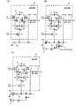
図2は、本発明の第1の実施形態における集積回路装置の構成を示す図であり、本発明の集積回路装置の基本的な構成例を示す。図2では、電圧比較を行う比較回路21を有する検出回路20と、ラッチ回路32を含む設定回路30とが設けられている。
図3に、本発明にかかる集積回路装置の第2の実施形態が示される。図3では、比較回路21による電圧比較に用いられるリファレンスとしての第1信号として、Lレベルがグランドレベルであるクロック信号SG1を使用する。つまり、図3においては、第1の端子T1は、第1信号としてのクロック信号SG1が入力されるクロック端子である。
図4に、本発明にかかる集積回路装置の第3の実施形態が示される。図4においては、第1信号端子T1、グランド端子TGの他に、イネーブル信号ENが入力されるイネーブル端子TEと、第2信号SG2が入力される第2端子T2と、が設けられる。イネーブル信号ENによって、内部回路200のイネーブル/ディスエーブルが切り換えられる。これによって、内部回路200の消費電力を削減することができる。また、イネーブル信号ENは、設定回路30内のラッチ回路32にも供給される。イネーブル信号ENが非アクティブとなって内部回路200がディスエーブル状態になったときは、内部回路200の誤動作する可能性はなくなるため、設定回路に設けられるラッチ回路も、そのタイミングでリセットするものである。
図7は、本発明の第4実施形態にかかる集積回路装置の要部構成を示す図である。図7においては、外部からリセット信号XRSTを、端子T4を経由してIC内に入力することができる。また、内部回路200は、リセット信号を受ける内部リセット端子T(RST)を有している。
図4に示されるように、電子機器900は、本発明にかかる集積回路装置(IC)10を含んでいる。本発明にかかる集積回路装置10は、電圧トレラント構造を有し、静電破壊耐量が高く、かつ、グランドオープン時の対策も万全であって信頼性が高い。よって、本発明にかかる集積回路装置10を搭載する電子機器900の信頼性も、同様に向上する。電子機器900は、例えば、携帯電話機、PDA等の携帯型情報端末である。
20 検出回路、21 比較回路(電圧比較回路)30 設定回路、
32 ラッチ回路、200 内部回路、 900 電子機器、
D11〜D42 静電保護素子(ダイオード)
Claims (6)
- 内部回路と、
グランド端子と、
前記内部回路が動作している期間の少なくとも一部の期間においてグランドレベルとなる第1信号が供給される第1端子と、
前記第1端子の電圧と、前記グランド端子の電圧とを比較することによって、前記グランド端子のオープン状態を検出する検出回路と、
前記検出回路によって前記グランド端子のオープン状態が検出されると、前記内部回路をリセットまたはディスエーブル状態に設定する設定回路と、
第2の端子と、
前記第2の端子を介して入力される第2信号を受けるI/Oセルと、を含み、
前記I/Oセルは、前記第2の端子と前記グランドとの間に設けられた静電保護素子を含み、
前記第2信号は、前記内部回路が動作している期間の少なくとも一部の期間においてグランドレベルとなる信号であることを特徴とする集積回路装置。 - 請求項1において、
前記検出回路は、
前記第1端子の電圧が制御ノードに供給される、第1導電型の第1トランジスターと、
前記グランド端子の電圧が制御ノードに供給され、第1導電型であり、かつ、前記第1トランジスターと差動対を構成する第2トランジスターと、
前記第1トランジスターと前記第2トランジスターとで構成される前記差動対の負荷であるカレントミラー回路と、
前記差動対および前記カレントミラー回路の動作電流を供給する電流源トランジスターとしての第3トランジスターと、
を有する電圧比較回路を含むことを特徴とする集積回路装置。 - 請求項1又は請求項2において、
前記設定回路は、前記検出回路によって前記グランド端子のオープン状態が検出されると、前記内部回路をリセットまたはディスエーブル状態に設定するための動作状態制御信号のレベルを、前記内部回路がイネーブル状態となっている期間中においてアクティブレベルに保持するラッチ回路を有することを特徴とする集積回路装置。 - 請求項3において、
前記内部回路のイネーブル/ディスエーブルを切り換えるためのイネーブル信号を入力するためのイネーブル端子を有し、
前記イネーブル信号がアクティブレベルから非アクティブレベルに変化して、前記内部回路がイネーブル状態からディスエーブル状態となると、前記ラッチ回路もリセットされることを特徴とする集積回路装置。 - 内部回路と、
グランド端子と、
前記内部回路が動作している期間の少なくとも一部の期間においてグランドレベルとなる第1信号が供給される第1端子と、
前記第1端子の電圧と、前記グランド端子の電圧とを比較することによって、前記グランド端子のオープン状態を検出する検出回路と、
前記検出回路によって前記グランド端子のオープン状態が検出されると、前記内部回路をリセットまたはディスエーブル状態に設定する設定回路と、を含み、
前記第1の端子は、前記第1信号としてのクロック信号が入力されるクロック端子であることを特徴とする集積回路装置。 - 請求項1〜請求項5のいずれかに記載の集積回路装置を含むことを特徴とする電子機器。
Priority Applications (2)
| Application Number | Priority Date | Filing Date | Title |
|---|---|---|---|
| JP2009022711A JP4670972B2 (ja) | 2009-02-03 | 2009-02-03 | 集積回路装置、及び電子機器 |
| US12/697,514 US8183897B2 (en) | 2009-02-03 | 2010-02-01 | Integrated circuit device and electronic apparatus |
Applications Claiming Priority (1)
| Application Number | Priority Date | Filing Date | Title |
|---|---|---|---|
| JP2009022711A JP4670972B2 (ja) | 2009-02-03 | 2009-02-03 | 集積回路装置、及び電子機器 |
Publications (2)
| Publication Number | Publication Date |
|---|---|
| JP2010183168A JP2010183168A (ja) | 2010-08-19 |
| JP4670972B2 true JP4670972B2 (ja) | 2011-04-13 |
Family
ID=42397187
Family Applications (1)
| Application Number | Title | Priority Date | Filing Date |
|---|---|---|---|
| JP2009022711A Active JP4670972B2 (ja) | 2009-02-03 | 2009-02-03 | 集積回路装置、及び電子機器 |
Country Status (2)
| Country | Link |
|---|---|
| US (1) | US8183897B2 (ja) |
| JP (1) | JP4670972B2 (ja) |
Families Citing this family (7)
| Publication number | Priority date | Publication date | Assignee | Title |
|---|---|---|---|---|
| JP5206571B2 (ja) * | 2009-04-22 | 2013-06-12 | 富士通セミコンダクター株式会社 | グランドオープン検出回路を有する集積回路装置 |
| JP5678542B2 (ja) * | 2010-09-24 | 2015-03-04 | 富士通セミコンダクター株式会社 | 電源状態判定回路を有する集積回路 |
| JP5739729B2 (ja) * | 2011-05-31 | 2015-06-24 | ルネサスエレクトロニクス株式会社 | 半導体装置、電子機器、および半導体装置の検査方法 |
| JP6182329B2 (ja) * | 2013-02-28 | 2017-08-16 | ルネサスエレクトロニクス株式会社 | 半導体装置 |
| EP2919262B1 (en) * | 2014-03-14 | 2022-12-21 | EM Microelectronic-Marin SA | Fault detection assembly |
| JP2018014561A (ja) * | 2016-07-19 | 2018-01-25 | 富士電機株式会社 | 半導体装置 |
| CN117475961A (zh) * | 2023-12-13 | 2024-01-30 | 北京集创北方科技股份有限公司 | 显示驱动电路及芯片、设备 |
Family Cites Families (7)
| Publication number | Priority date | Publication date | Assignee | Title |
|---|---|---|---|---|
| JP2885967B2 (ja) * | 1991-06-27 | 1999-04-26 | 三菱電機エンジニアリング株式会社 | 電気回路装置 |
| JPH0883909A (ja) * | 1994-09-09 | 1996-03-26 | Mitsubishi Electric Corp | 半導体集積回路 |
| US5933077A (en) * | 1997-06-20 | 1999-08-03 | Wells Fargo Alarm Services, Inc. | Apparatus and method for detecting undesirable connections in a system |
| US6144221A (en) | 1998-07-02 | 2000-11-07 | Seiko Epson Corporation | Voltage tolerant interface circuit |
| JP2002259357A (ja) * | 2001-03-02 | 2002-09-13 | Mitsubishi Electric Corp | マイクロコンピュータ |
| CN100358240C (zh) * | 2002-10-21 | 2007-12-26 | Nxp股份有限公司 | 防故障方法和电路 |
| DE102007040856B4 (de) * | 2007-08-29 | 2009-04-23 | Texas Instruments Deutschland Gmbh | Komparator mit Empfindlichkeitssteuerung |
-
2009
- 2009-02-03 JP JP2009022711A patent/JP4670972B2/ja active Active
-
2010
- 2010-02-01 US US12/697,514 patent/US8183897B2/en active Active
Also Published As
| Publication number | Publication date |
|---|---|
| US20100194452A1 (en) | 2010-08-05 |
| JP2010183168A (ja) | 2010-08-19 |
| US8183897B2 (en) | 2012-05-22 |
Similar Documents
| Publication | Publication Date | Title |
|---|---|---|
| JP4670972B2 (ja) | 集積回路装置、及び電子機器 | |
| KR101885334B1 (ko) | 정전기 방전 보호 회로 | |
| KR101870995B1 (ko) | 반도체 집적회로의 esd 보호 회로 | |
| US10158225B2 (en) | ESD protection system utilizing gate-floating scheme and control circuit thereof | |
| US20160064926A1 (en) | Esd protecting circuit | |
| CN1822501B (zh) | 没有静电放电电压的耐高输入电压的输入/输出电路 | |
| CN101273507B (zh) | 保护ic组件的系统和方法 | |
| US8243404B2 (en) | ESD protection circuit with merged triggering mechanism | |
| KR20080076411A (ko) | 정전기 보호 회로 | |
| KR102852456B1 (ko) | 정전기 보호 회로 | |
| US9263882B2 (en) | Output circuits with electrostatic discharge protection | |
| US10965116B2 (en) | Overvoltage-proof circuit capable of preventing damage caused by overvoltage | |
| US8018698B2 (en) | I/O circuit with ESD protecting function | |
| US9312691B2 (en) | ESD protection circuit and ESD protection method thereof | |
| TW201401478A (zh) | 防止跨越電壓域之靜電放電失效 | |
| JP2008283274A (ja) | 入力インタフェース回路、集積回路装置および電子機器 | |
| US20100149704A1 (en) | Esd protection circuit | |
| US8363366B2 (en) | Electrostatic discharge protection circuit | |
| JP5082841B2 (ja) | 半導体装置 | |
| JP3875984B2 (ja) | 複数の電源を有する電子システムのための過渡電圧検出回路 | |
| KR100650816B1 (ko) | 내부 회로 보호 장치 | |
| US7295039B2 (en) | Buffer circuit | |
| KR100364130B1 (ko) | 정전기 보호회로 | |
| KR20080111670A (ko) | 정전기 방전 보호 회로 및 이를 포함하는 반도체 장치 | |
| JP2013045993A (ja) | 半導体集積回路装置 |
Legal Events
| Date | Code | Title | Description |
|---|---|---|---|
| A131 | Notification of reasons for refusal |
Free format text: JAPANESE INTERMEDIATE CODE: A131 Effective date: 20101005 |
|
| A521 | Request for written amendment filed |
Free format text: JAPANESE INTERMEDIATE CODE: A523 Effective date: 20101202 |
|
| TRDD | Decision of grant or rejection written | ||
| A01 | Written decision to grant a patent or to grant a registration (utility model) |
Free format text: JAPANESE INTERMEDIATE CODE: A01 Effective date: 20101221 |
|
| A01 | Written decision to grant a patent or to grant a registration (utility model) |
Free format text: JAPANESE INTERMEDIATE CODE: A01 |
|
| A61 | First payment of annual fees (during grant procedure) |
Free format text: JAPANESE INTERMEDIATE CODE: A61 Effective date: 20110103 |
|
| R150 | Certificate of patent or registration of utility model |
Ref document number: 4670972 Country of ref document: JP Free format text: JAPANESE INTERMEDIATE CODE: R150 Free format text: JAPANESE INTERMEDIATE CODE: R150 |
|
| FPAY | Renewal fee payment (event date is renewal date of database) |
Free format text: PAYMENT UNTIL: 20140128 Year of fee payment: 3 |
|
| S531 | Written request for registration of change of domicile |
Free format text: JAPANESE INTERMEDIATE CODE: R313531 |
|
| R350 | Written notification of registration of transfer |
Free format text: JAPANESE INTERMEDIATE CODE: R350 |
|
| S111 | Request for change of ownership or part of ownership |
Free format text: JAPANESE INTERMEDIATE CODE: R313113 |
|
| R350 | Written notification of registration of transfer |
Free format text: JAPANESE INTERMEDIATE CODE: R350 |
|
| S111 | Request for change of ownership or part of ownership |
Free format text: JAPANESE INTERMEDIATE CODE: R313113 |
|
| R350 | Written notification of registration of transfer |
Free format text: JAPANESE INTERMEDIATE CODE: R350 |
|
| R250 | Receipt of annual fees |
Free format text: JAPANESE INTERMEDIATE CODE: R250 |
|
| R250 | Receipt of annual fees |
Free format text: JAPANESE INTERMEDIATE CODE: R250 |