JP4670972B2 - Integrated circuit device and electronic device - Google Patents
Integrated circuit device and electronic device Download PDFInfo
- Publication number
- JP4670972B2 JP4670972B2 JP2009022711A JP2009022711A JP4670972B2 JP 4670972 B2 JP4670972 B2 JP 4670972B2 JP 2009022711 A JP2009022711 A JP 2009022711A JP 2009022711 A JP2009022711 A JP 2009022711A JP 4670972 B2 JP4670972 B2 JP 4670972B2
- Authority
- JP
- Japan
- Prior art keywords
- circuit
- terminal
- signal
- ground
- level
- Prior art date
- Legal status (The legal status is an assumption and is not a legal conclusion. Google has not performed a legal analysis and makes no representation as to the accuracy of the status listed.)
- Active
Links
- 238000001514 detection method Methods 0.000 claims description 33
- 230000007257 malfunction Effects 0.000 description 9
- 238000010586 diagram Methods 0.000 description 7
- 230000004048 modification Effects 0.000 description 3
- 238000012986 modification Methods 0.000 description 3
- 239000004065 semiconductor Substances 0.000 description 3
- 239000000872 buffer Substances 0.000 description 2
- 230000015556 catabolic process Effects 0.000 description 2
- 230000006698 induction Effects 0.000 description 2
- 230000001788 irregular Effects 0.000 description 2
- 101150110971 CIN7 gene Proteins 0.000 description 1
- 101100286980 Daucus carota INV2 gene Proteins 0.000 description 1
- 101150110298 INV1 gene Proteins 0.000 description 1
- 101100397044 Xenopus laevis invs-a gene Proteins 0.000 description 1
- 101100397045 Xenopus laevis invs-b gene Proteins 0.000 description 1
- 230000002159 abnormal effect Effects 0.000 description 1
- 230000000694 effects Effects 0.000 description 1
- 239000012212 insulator Substances 0.000 description 1
- 230000010354 integration Effects 0.000 description 1
- 230000001681 protective effect Effects 0.000 description 1
Images


Classifications
-
- H—ELECTRICITY
- H03—ELECTRONIC CIRCUITRY
- H03K—PULSE TECHNIQUE
- H03K19/00—Logic circuits, i.e. having at least two inputs acting on one output; Inverting circuits
- H03K19/003—Modifications for increasing the reliability for protection
-
- H—ELECTRICITY
- H03—ELECTRONIC CIRCUITRY
- H03K—PULSE TECHNIQUE
- H03K19/00—Logic circuits, i.e. having at least two inputs acting on one output; Inverting circuits
- H03K19/003—Modifications for increasing the reliability for protection
- H03K19/00369—Modifications for compensating variations of temperature, supply voltage or other physical parameters
Description
本発明は、集積回路装置、及び電子機器等に関する。 The present invention relates to an integrated circuit device, an electronic device, and the like.
近年、半導体集積回路装置の高集積化及び低消費電力化を図るために、電源電圧の異なる複数のLSIが接続されたり、あるいは電源電圧の異なる回路が同一チップ上に搭載されることがある。このため、入出力回路は入出力端子に電源電圧より高い電圧の入力信号が入力されても支障なく動作するトレラント入出力回路とする必要がある。このようなトレラント入出力回路の一例として、回路内部の電源電位とは異なる、より高電位の電位を外部から受ける可能性のある入出力回路として使用される電圧トレラント回路が特許文献1に開示されている。このような半導体集積回路装置のI/O部に設けられるI/Oセルには、外部からの静電誘導電圧や過電流などの電気的なストレスに対して当該半導体集積回路装置を保護するための静電保護素子(静電保護ダイオード等)が設けられている。
In recent years, in order to achieve high integration and low power consumption of semiconductor integrated circuit devices, a plurality of LSIs having different power supply voltages may be connected or circuits having different power supply voltages may be mounted on the same chip. Therefore, the input / output circuit needs to be a tolerant input / output circuit that operates without any problem even when an input signal having a voltage higher than the power supply voltage is input to the input / output terminal. As an example of such a tolerant input / output circuit,
本発明の発明者は、絶縁性異物の付着等によって、グランド線(低電位電源線)がオープン状態(フローティング状態)となった場合における、集積回路装置(IC)の内部回路の挙動について検討した。この結果、グランド線がオープン状態となった場合においても、静電保護ダイオードを経由する電流パスが構成されて、内部回路が動作してしまう場合があることが明らかとなった。 The inventor of the present invention examined the behavior of the internal circuit of the integrated circuit device (IC) when the ground line (low-potential power line) is in an open state (floating state) due to adhesion of insulating foreign matter or the like. . As a result, it has been clarified that even when the ground line is in an open state, a current path passing through the electrostatic protection diode is formed and the internal circuit may operate.
但し、電流パスが構成されるのは、静電保護ダイオードに接続される端子(グランド端子以外の端子)の電位がL(=GND)のときだけであり、その端子の電位がHとなると電流パスは形成されず、内部回路は動作しなくなる。 However, the current path is configured only when the potential of a terminal (terminal other than the ground terminal) connected to the electrostatic protection diode is L (= GND). A path is not formed and the internal circuit does not operate.
すなわち、グランド線がオープン状態となったとき、他の端子の電位がLレベルのときは内部回路が動作し、Hレベルのときは内部回路が動作しないという、正常ではない回路動作が生じる場合があることがわかった。この場合、ICの内部回路の動作/非動作は、静電保護ダイオードに接続される端子の電位によって決定されることになり、ICの信頼性を担保できなくなる。 That is, when the ground line is in an open state, an abnormal circuit operation may occur in which the internal circuit operates when the potential of the other terminal is L level, and the internal circuit does not operate when the potential of the other terminal is H level. I found out. In this case, the operation / non-operation of the internal circuit of the IC is determined by the potential of the terminal connected to the electrostatic protection diode, and the reliability of the IC cannot be ensured.
本発明に係る幾つかの態様によれば、例えば、グランド線がオープン状態となった場合であっても、グランド端子以外の端子の電位に応じて、内部回路の動作/非動作が決定されてしまうような不都合が生じないようにすることができ、ICの信頼性を向上することができる。 According to some aspects of the present invention, for example, even when the ground line is in an open state, the operation / non-operation of the internal circuit is determined according to the potential of a terminal other than the ground terminal. Such an inconvenience can be prevented, and the reliability of the IC can be improved.
本発明の一態様は、内部回路と、グランド端子と、前記内部回路が動作している期間の少なくとも一部の期間においてグランドレベルとなる第1信号が供給される第1端子と、前記第1端子の電圧と、前記グランド端子の電圧とを比較することによって、前記グランド端子のオープン状態を検出する検出回路と、前記検出回路によって前記グランド端子のオープン状態が検出されると、前記内部回路をリセットまたはディスエーブル状態に設定する設定回路と、を含む集積回路装置に関係する。 One embodiment of the present invention includes an internal circuit, a ground terminal, a first terminal to which a first signal that is at a ground level in at least a part of a period in which the internal circuit is operating, and the first terminal. A detection circuit that detects the open state of the ground terminal by comparing the voltage of the terminal and the voltage of the ground terminal; and when the open state of the ground terminal is detected by the detection circuit, the internal circuit And a setting circuit for setting to a reset or disabled state.
グランド端子がオープン状態になった状態において、他の端子を経由した非正規の電流パスを経由して動作電流(グランド電流)が流れるときは、グランド端子のレベルは、正規のグランドレベルとは一致しない。よって、正規のグランド端子の電位を、リファレンス信号としての第1信号が入力される第1端子の電位と比較することによって、グランド端子の電位が、正常なグランドレベル(リファレンスとしての第1信号のグランドレベル)と一致するか異なっているかを検出することができる。電圧が異なっている場合には、グランド端子がオープン状態となっているため、内部回路をリセットまたはディスエーブル状態とする。これによって、内部回路の誤動作が防止される。第1信号は、グランド端子に供給されるグランドとは別系統のグランドであってよく、また、Lレベルがグランドレベルであるクロック信号等であってもよい。 When the operating current (ground current) flows through the non-regular current path via other terminals in the open state of the ground terminal, the level of the ground terminal matches the normal ground level. do not do. Therefore, by comparing the potential of the normal ground terminal with the potential of the first terminal to which the first signal as the reference signal is input, the potential of the ground terminal is set to the normal ground level (the first signal as the reference). It can be detected whether it matches or is different from the (ground level). When the voltages are different, since the ground terminal is in an open state, the internal circuit is reset or disabled. This prevents malfunction of the internal circuit. The first signal may be a ground of a different system from the ground supplied to the ground terminal, or may be a clock signal or the like whose L level is the ground level.
また、本発明の第2の態様は、第2の端子と、前記第2の端子を介して入力される第2信号を受けるI/Oセルと、を含み、前記I/Oセルは、前記第2の端子と前記グランドとの間に設けられた静電保護素子を含み、前記第2信号は、前記内部回路が動作している期間の少なくとも一部の期間においてグランドレベルとなる信号である集積回路装置に関係する。 The second aspect of the present invention includes a second terminal and an I / O cell that receives a second signal input via the second terminal, and the I / O cell includes: An electrostatic protection element provided between a second terminal and the ground is included, and the second signal is a signal that is at a ground level during at least a part of a period in which the internal circuit is operating. Related to integrated circuit devices.
グランド端子がオープン状態のときに、第2端子がグランドレベルとなると、その第2端子が疑似的なグランド端子として機能し、I/Oセルに含まれる静電保護素子(静電保護ダイオード等を含む)を経由した非正規の電流パスが形成され、動作電流(グランド電流)が流れてしまう。この場合でも、検出回路がグランド端子のオープン状態を確実に検出し、これに伴い、内部回路がリセット状態(ディスエーブル状態)になるため、内部回路の誤動作は確実に防止される。 When the second terminal is at the ground level when the ground terminal is in an open state, the second terminal functions as a pseudo ground terminal, and an electrostatic protection element (an electrostatic protection diode or the like) included in the I / O cell is used. A non-regular current path is formed through the operation current, and an operating current (ground current) flows. Even in this case, the detection circuit reliably detects the open state of the ground terminal, and accordingly, the internal circuit is in the reset state (disabled state), so that the malfunction of the internal circuit is reliably prevented.
また、本発明の他の態様は、前記検出回路は、前記第1端子の電圧が制御ノードに供給される、第1導電型の第1トランジスターと、前記グランド端子の電圧が制御ノードに供給され、第1導電型であり、かつ、前記第1トランジスターと差動対を構成する第2トランジスターと、前記第1トランジスターと前記第2トランジスターとで構成される前記差動対の負荷であるカレントミラー回路と、前記差動対および前記カレントミラー回路の動作電流を供給する電流源トランジスターとしての第3トランジスターと、を有する電圧比較回路を含む集積回路装置に関係する。 According to another aspect of the present invention, the detection circuit is configured such that the voltage of the first terminal is supplied to the control node, the first conductivity type first transistor, and the voltage of the ground terminal is supplied to the control node. And a current mirror that is a load of the differential pair that is of the first conductivity type and that includes the second transistor that forms a differential pair with the first transistor, and the first transistor and the second transistor. The present invention relates to an integrated circuit device including a voltage comparison circuit having a circuit and a third transistor as a current source transistor that supplies an operation current of the differential pair and the current mirror circuit.
差動対トランジスターとカレントミラー負荷、ならびに電流源トランジスターによって構成される電圧比較回路を、検出回路として用いることによって、コンパクトな回路で、グランド端子のオープン状態を確実に検出することができる。 By using a voltage comparison circuit constituted by a differential pair transistor, a current mirror load, and a current source transistor as a detection circuit, the open state of the ground terminal can be reliably detected with a compact circuit.
また、本発明の他の態様は、前記設定回路は、前記検出回路によって前記グランド端子のオープン状態が検出されると、前記内部回路をリセットまたはディスエーブル状態に設定するための動作状態制御信号のレベルを、前記内部回路がイネーブル状態となっている期間中においてアクティブレベルに保持するラッチ回路を有する集積回路装置に関係する。 Further, according to another aspect of the present invention, the setting circuit includes an operation state control signal for resetting or disabling the internal circuit when the detection circuit detects an open state of the ground terminal. The present invention relates to an integrated circuit device having a latch circuit that holds a level at an active level during a period in which the internal circuit is enabled.
内部回路の動作中において、1回でもグランド端子のオープンが検出されたときは、その内部回路が、イネーブル信号によってイネーブル状態とされる期間中、リセットまたはディスエーブル状態に保持するのが好ましい。したがって、本態様では、内部回路をリセットまたはディスエーブル状態に設定するための動作状態制御信号のレベルを、内部回路がイネーブル状態となっている期間中においてアクティブレベルに保持するためのラッチ回路を設ける。これによって、一旦、グランド端子のオープンが検出されて内部回路がリセット状態等になると、その後のグランド端子の状態に関係なく、一律に内部回路は動作できなくなるため、内部回路の誤動作は確実に防止される。 When the opening of the ground terminal is detected even once during the operation of the internal circuit, the internal circuit is preferably held in the reset or disabled state during the period of being enabled by the enable signal. Therefore, in this aspect, a latch circuit is provided for holding the level of the operation state control signal for setting the internal circuit in the reset or disabled state at an active level during the period in which the internal circuit is in the enable state. . As a result, once the opening of the ground terminal is detected and the internal circuit is in a reset state, etc., the internal circuit cannot be operated uniformly regardless of the state of the subsequent ground terminal. Is done.
また、本発明の他の態様は、前記内部回路のイネーブル/ディスエーブルを切り換えるためのイネーブル信号を入力するためのイネーブル端子を有し、前記イネーブル信号がアクティブレベルから非アクティブレベルに変化して、前記内部回路がイネーブル状態からディスエーブル状態となると、前記ラッチ回路もリセットされる集積回路装置に関係する。 According to another aspect of the present invention, there is an enable terminal for inputting an enable signal for switching enable / disable of the internal circuit, and the enable signal changes from an active level to an inactive level, When the internal circuit changes from the enable state to the disable state, the latch circuit also relates to the integrated circuit device that is reset.
イネーブル信号が非アクティブとなって内部回路がディスエーブル状態になったときは、内部回路の誤動作する可能性はなくなるため、設定回路に設けられるラッチ回路も、そのタイミングでリセットするものである。 When the enable signal becomes inactive and the internal circuit is disabled, there is no possibility of malfunction of the internal circuit, so the latch circuit provided in the setting circuit is also reset at that timing.
また、本発明の他の態様は、前記第1の端子は、前記第1信号としてのクロック信号が入力されるクロック端子である集積回路装置に関係する。 Another aspect of the invention relates to an integrated circuit device in which the first terminal is a clock terminal to which a clock signal as the first signal is input.
第1信号(電圧比較のためのリファレンス)として、Lレベルがグランドレベルであるクロック信号を使用することによって、リファレンス信号を別途、用意する必要がなく、実用上、有利となる。 By using a clock signal whose L level is the ground level as the first signal (reference for voltage comparison), it is not necessary to prepare a reference signal separately, which is practically advantageous.
また、本発明の他の態様は、上記いずれかの集積回路装置を含む電子機器に関係する。 Another aspect of the invention relates to an electronic apparatus including any one of the above integrated circuit devices.
本発明にかかる集積回路装置は、電圧トレラント構造を有し、静電破壊耐量が高く、かつ、グランドオープン時の対策も万全であって信頼性が高い。よって、本発明にかかる集積回路装置を搭載する電子機器の信頼性も、同様に向上する。 The integrated circuit device according to the present invention has a voltage-tolerant structure, has a high resistance to electrostatic breakdown, and is fully reliable in measures against a ground open, and has high reliability. Therefore, the reliability of the electronic equipment equipped with the integrated circuit device according to the present invention is also improved.
以下、本発明の好適な実施の形態について詳細に説明する。なお、以下に説明する本実施形態は、特許請求の範囲に記載された本発明の内容を不当に限定するものではなく、本実施形態で説明される構成の全てが本発明の解決手段として必須であるとは限らない。 Hereinafter, preferred embodiments of the present invention will be described in detail. The present embodiment described below does not unduly limit the contents of the present invention described in the claims, and all the configurations described in the present embodiment are essential as means for solving the present invention. Not necessarily.
1.内部回路の誤動作が生じる現象についての説明
本発明は、本発明前に、本発明の発明者によって明らかとされたグランド端子がオープンとなった場合の回路の動作不良の問題となった現象に関する知見に基づいてなされたものである。よって、本発明の実施形態にかかる集積回路装置の構成と動作について説明する前に、本発明前に、本発明者によって検討された回路、及びグランド端子がオープンとなったときに生じた問題の発生原因等について説明する。
1. Description of phenomenon that causes malfunction of internal circuit Prior to the present invention, the present invention relates to the knowledge about the phenomenon that caused the malfunction of the circuit when the ground terminal opened by the inventor of the present invention was opened. It was made based on. Therefore, before describing the configuration and operation of the integrated circuit device according to the embodiment of the present invention, before the present invention, the circuit studied by the present inventor and the problem caused when the ground terminal is opened. The cause of occurrence will be described.
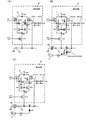
以下、図1(A)、図1(B)を用いて、本発明前に、本発明者によって検討された回路および検討結果等について説明する。 Hereinafter, the circuit, the examination result, and the like studied by the inventor before the present invention will be described with reference to FIG. 1 (A) and FIG. 1 (B).
集積回路装置のI/O部に設けられるI/Oセル13には、外部からの静電誘導電圧や過電流などの電気的なストレスに対して当該集積回路装置や内部回路等を保護するための静電気保護素子(静電保護ダイオードD31、D32、電流制限抵抗R3等)設けられている。また、BF3は、信号入力用の入力バッファである。
The I /
このため、低電位側電源となるグランド(GND)の入力端子であるグランド端子TGに絶縁物OB等が付着して電源がオープンになった時でも、図1(A)に示されるように、静電保護ダイオードD32に接続される端子T2に供給される信号SG2がLレベル(グランドレベル)である場合には、端子T2が疑似的なグランド端子として機能し、動作電流(グランド電流)I1が流れる場合がある。この場合、グランド線L1の電位は、GND+Vf(D32)(Vf(D32)は、静電保護ダイオードD32の順方向電圧である)となるが、Vf(D32)が例えば、数百mV程度と低い場合には、グランド線L1の電位はそれほど上昇せず、よって、内部回路200は動作してしまう。
Therefore, even when an insulator OB or the like adheres to the ground terminal TG which is an input terminal of the ground (GND) serving as the low potential side power supply and the power supply is opened, as shown in FIG. When the signal SG2 supplied to the terminal T2 connected to the electrostatic protection diode D32 is at L level (ground level), the terminal T2 functions as a pseudo ground terminal, and the operating current (ground current) I1 is May flow. In this case, the potential of the ground line L1 is GND + Vf (D32) (Vf (D32) is a forward voltage of the electrostatic protection diode D32), but Vf (D32) is as low as about several hundred mV, for example. In this case, the potential of the ground line L1 does not rise so much, and thus the
一方、図1(B)に示されるように、端子T2に供給される信号SG2がHレベル(例えば、VDDレベル)である場合には、非正規の電流パスは構成されない。よって、内部回路200は動作しない。
On the other hand, as shown in FIG. 1B, when the signal SG2 supplied to the terminal T2 is at the H level (for example, the VDD level), an irregular current path is not configured. Therefore, the
上述のケースでは、ICの内部回路の動作/非動作は、静電保護ダイオードD32に接続される端子T2の電位によって決定されることになり、ICの信頼性を担保できなくなる。 In the above case, the operation / non-operation of the internal circuit of the IC is determined by the potential of the terminal T2 connected to the electrostatic protection diode D32, and the reliability of the IC cannot be ensured.
2.集積回路装置
2.1.第1の実施形態
図2は、本発明の第1の実施形態における集積回路装置の構成を示す図であり、本発明の集積回路装置の基本的な構成例を示す。図2では、電圧比較を行う比較回路21を有する検出回路20と、ラッチ回路32を含む設定回路30とが設けられている。
2. Integrated circuit device 2.1. First Embodiment FIG. 2 is a diagram showing a configuration of an integrated circuit device according to a first embodiment of the present invention, and shows a basic configuration example of an integrated circuit device of the present invention. In FIG. 2, a
グランド端子がオープン状態になった状態において、グランド端子TGとは別の他の端子T2を経由した非正規の電流パスを経由して動作電流(グランド電流)が流れるときは、グランド端子TGの電圧レベルは、正規のグランドレベル(GND)とは一致しない。つまり、静電保護ダイオードD32の順方向電圧Vf(D32)分だけ上昇する。よって、正規のグランド端子TGの電位を、リファレンス信号としての第1信号(GND2)が入力される第1端子T1の電位と比較することによって、グランド端子TGの電位が、正常なグランドレベル(リファレンスとしての第1信号GND2のグランドレベル)と一致するか異なっているかを検出することができる。 When an operating current (ground current) flows through an irregular current path via another terminal T2 other than the ground terminal TG in a state where the ground terminal is in an open state, the voltage of the ground terminal TG The level does not match the normal ground level (GND). That is, it increases by the forward voltage Vf (D32) of the electrostatic protection diode D32. Therefore, by comparing the potential of the normal ground terminal TG with the potential of the first terminal T1 to which the first signal (GND2) as the reference signal is input, the potential of the ground terminal TG is changed to a normal ground level (reference It is possible to detect whether the first signal GND2 is equal to or different from the ground level of the first signal GND2.
この電圧比較は、検出回路20に含まれる比較回路21によって実行される。その電圧比較の結果、電圧が異なっている場合(つまり、グランド端子TGの電位が、リファレンスとしての第1信号GND2のグランドレベルよりも高い場合)には、グランド端子TGがオープン状態となっている。よって、この場合には、設定回路30は、リセット信号RXまたはディスエーブル設定信号DXを内部回路200に向けて出力して、内部回路200をリセット状態またはディスエーブル状態とする。なお、設定回路30は、内部回路200の動作状態を設定する働きをする。
This voltage comparison is performed by a
これによって、内部回路200の誤動作が防止される。電圧比較時のリファレンスとして機能する第1信号(GND2)は、グランド端子TGに供給されるグランド(GND)とは別系統のグランド(GND2)であってよく、また、Lレベルがグランドレベルであるクロック信号等であってもよい。
As a result, malfunction of the
また、設定回路30は、検出回路20によってグランド端子TGのオープン状態が検出されると、内部回路200をリセットまたはディスエーブル状態に設定するための動作状態制御信号(上述のRXやDX)の電圧レベルを、内部回路200がイネーブル状態(つまり、動作可能状態)となっている期間中においてアクティブレベルに保持するラッチ回路32を有している。
In addition, when the
すなわち、内部回路200の動作中において、1回でもグランド端子TGのオープンが検出されたときは、その内部回路200が、イネーブル状態とされる期間中、リセットまたはディスエーブル状態に保持するのが好ましい。したがって、図2の例では、内部回路200をリセットまたはディスエーブル状態に設定するための動作状態制御信号(RXやDX)の電圧レベルを、内部回路200がイネーブル状態となっている期間中においてアクティブレベルに保持するためのラッチ回路32が設けられる。これによって、一旦、グランド端子TGのオープンが検出されて内部回路200がリセット状態等になると、その後のグランド端子TGの状態に関係なく、一律に内部回路200は動作できなくなるため、内部回路200の誤動作は確実に防止される。
That is, when the opening of the ground terminal TG is detected even once during the operation of the
2.2.第2の実施形態
図3に、本発明にかかる集積回路装置の第2の実施形態が示される。図3では、比較回路21による電圧比較に用いられるリファレンスとしての第1信号として、Lレベルがグランドレベルであるクロック信号SG1を使用する。つまり、図3においては、第1の端子T1は、第1信号としてのクロック信号SG1が入力されるクロック端子である。
2.2. Second Embodiment FIG. 3 shows a second embodiment of an integrated circuit device according to the present invention. In FIG. 3, the clock signal SG <b> 1 whose L level is the ground level is used as the first signal as a reference used for voltage comparison by the
第1信号(電圧比較のためのリファレンス)として、Lレベルがグランドレベルであるクロック信号SG1を使用することによって、特別なリファレンス信号を別途、用意する必要がなく、実用上、有利となる。 By using the clock signal SG1 whose L level is the ground level as the first signal (reference for voltage comparison), it is not necessary to prepare a special reference signal separately, which is practically advantageous.
2.3.第3実施形態
図4に、本発明にかかる集積回路装置の第3の実施形態が示される。図4においては、第1信号端子T1、グランド端子TGの他に、イネーブル信号ENが入力されるイネーブル端子TEと、第2信号SG2が入力される第2端子T2と、が設けられる。イネーブル信号ENによって、内部回路200のイネーブル/ディスエーブルが切り換えられる。これによって、内部回路200の消費電力を削減することができる。また、イネーブル信号ENは、設定回路30内のラッチ回路32にも供給される。イネーブル信号ENが非アクティブとなって内部回路200がディスエーブル状態になったときは、内部回路200の誤動作する可能性はなくなるため、設定回路に設けられるラッチ回路も、そのタイミングでリセットするものである。
2.3. Third Embodiment FIG. 4 shows a third embodiment of the integrated circuit device according to the present invention. In FIG. 4, in addition to the first signal terminal T1 and the ground terminal TG, an enable terminal TE to which the enable signal EN is input and a second terminal T2 to which the second signal SG2 is input are provided. The enable / disable of the
また、第2信号としてのSG2は、内部回路200が動作している期間(イネーブル信号によって動作可能とされる期間)の少なくとも一部の期間においてグランドレベルとなる信号であり、図4の場合、第2信号SG2は、内部回路200に設けられるメモリ210への書き込みデータである。書き込みデータが0(L)は、グランドレベルに対応する。
SG2 as the second signal is a signal that is at the ground level in at least a part of the period in which the
また、図4において、各信号の入力部には、静電保護回路を備えるI/Oセル11〜13が設けられている。I/Oセル11、12の構成は、先に説明したI/Oセル13の構成と同様である。
In FIG. 4, I /
また、図4に示される検出回路20は、差動対トランジスター、カレントミラー、電流源トランジスター等で構成される電圧比較回路21を有している。すなわち、電圧比較回路21は、第1端子T1の電圧が制御ノード(ゲート)に供給される、第1導電型(P型)の第1トランジスターPT1と、グランド端子TGの電圧が制御ノード(ゲート)に供給され、第1導電型(P型)であり、かつ、第1トランジスターPT1と差動対を構成する第2トランジスターPT2と、第1トランジスターPT1と第2トランジスターPT2とで構成される差動対の負荷であるカレントミラー回路(N型の第3および第4トランジスターNT1、NT2により構成される)と、差動対およびカレントミラー回路の動作電流を供給する電流源トランジスターとしての第5トランジスター(N型トランジスター)NT3と、を有する。差動対トランジスターとカレントミラー負荷、ならびに電流源トランジスターによって構成される電圧比較回路21を、検出回路20として用いることによって、コンパクトな回路で、グランド端子のオープン状態を確実に検出することができる。なお、電圧比較回路21からは、シングルエンド検出出力Q1が得られ、この検出出力Q1は、出力バッファとしてのインバーターINV1、INV2を経由して、検出出力Q2として出力される。
Further, the
図5(A)〜図5(C)の各々は、図4に示される検出回路20の動作を説明するための図である。図5(A)では、グランド端子TGは、オープン状態とはなっていないため、差動トランジスターPT1、PT2の各々に同量の電流Id2、Id1が流れ、差動回路はバランスするため、検出出力Q1、Q2はLレベルとなる(バランス状態においては、出力がLになるように差動回路が構成されている)。
Each of FIGS. 5A to 5C is a diagram for explaining the operation of the
図5(B)では、先に説明したように、絶縁性異物OBの付着等によって、グランド端子TGがオープン状態となり、かつ、第2信号であるSG2がLレベルとなって、非正規の電流パスが構成され、動作電流I1が流れる。この場合、グランド端子TGの電圧レベルは、ダイオードD32の順方向電圧分だけ上昇することから、差動回路における左右のバランスがくずれ、Id2>Id1となる。よって、検出出力Q1、Q2はLレベルからHレベルに反転し、これによって、グランド端子TGのオープン状態が検出される。 In FIG. 5B, as described above, the ground terminal TG is in an open state due to the adhesion of the insulating foreign matter OB, and the second signal SG2 becomes L level, and the non-normal current A path is formed, and an operating current I1 flows. In this case, since the voltage level of the ground terminal TG increases by the forward voltage of the diode D32, the left and right balance in the differential circuit is lost, and Id2> Id1. Therefore, the detection outputs Q1 and Q2 are inverted from the L level to the H level, thereby detecting the open state of the ground terminal TG.
また、図5(C)では、絶縁性異物OBの付着等によって、グランド端子TGがオープン状態となり、かつ、第2信号であるSG2がHレベルであるため、動作電流(グランド電流)が流れることができない。よって、検出回路20自体が正常に動作し得ない。但し、高電位電源電圧VDDは検出回路20に印加されていることから、結果的に、検出出力Q1、Q2はHレベルとなる。
In FIG. 5C, the ground terminal TG is in an open state due to the adhesion of the insulating foreign object OB and the second signal SG2 is at the H level, so that an operating current (ground current) flows. I can't. Therefore, the
図5(B)、図5(C)からわかるように、グランド端子TGがオープン状態となったときは、検出出力Q1、Q2はHを維持するため、グランドのオープンを確実に検出することができる。 As can be seen from FIGS. 5B and 5C, when the ground terminal TG is in the open state, the detection outputs Q1 and Q2 are maintained at H, so that it is possible to reliably detect the open of the ground. it can.
図6は、図4に示される回路の動作を説明するための図である。時刻t1において、イネーブル信号ENがLレベルからHレベル(アクティブレベル)に変化すると、内部回路200がイネーブル状態(動作可能状態)となる。また、第2端子T2に供給される第2信号のレベルが、時刻t2において、例えばHからLに変化する。グランド端子TGがオープン状態となっていると、グランド端子TGのレベルはフローティング状態となるものの、上述のとおり、例えば、静電保護ダイオードを経由して電流パスが構成されることから、その電位が上昇する傾向が生じる。先に説明したように、電圧比較回路におけるリファレンスとして機能する第1信号SG1がLレベルの期間において、グランド端子TGの電圧レベルを、リファレンスとしてのグランドレベルと比較することができる。よって、第1信号SG1がLレベルの期間が検出期間(T(DE))となる。時刻t4において、検出出力Q2がHレベルに反転する。この時刻t4のタイミングで、設定回路30内のラッチ回路32において、検出結果が保持される。よって、時刻t4において、内部回路200のリセット信号DX(あるいはディスエーブル信号DX)がアクティブレベルとなる。時刻t6において、イネーブル信号ENが非アクティブレベル(L)となると、内部回路200のリセット信号DX(あるいはディスエーブル信号DX)も非アクティブとなる。
FIG. 6 is a diagram for explaining the operation of the circuit shown in FIG. When the enable signal EN changes from the L level to the H level (active level) at time t1, the
2.4.第4実施形態
図7は、本発明の第4実施形態にかかる集積回路装置の要部構成を示す図である。図7においては、外部からリセット信号XRSTを、端子T4を経由してIC内に入力することができる。また、内部回路200は、リセット信号を受ける内部リセット端子T(RST)を有している。
2.4. Fourth Embodiment FIG. 7 is a diagram showing a main configuration of an integrated circuit device according to a fourth embodiment of the present invention. In FIG. 7, the reset signal XRST can be input from the outside into the IC via the terminal T4. The
また、外部から供給されるリセット信号XRST、および、設定回路30から出力されるリセット信号DX(あるいはディスエーブル信号DX)は各々、ゲート回路215を経由して、内部回路200の内部リセット端子T(RST)に入力される。本実施形態では、グランド端子TGのオープンが検出されたときに、内部リセット端子T(RST)を活用して内部回路200をリセットする。よって、内部的なリセット端子を特別に設ける必要がない。
Further, the reset signal XRST supplied from the outside and the reset signal DX (or disable signal DX) output from the setting
3.電子機器
図4に示されるように、電子機器900は、本発明にかかる集積回路装置(IC)10を含んでいる。本発明にかかる集積回路装置10は、電圧トレラント構造を有し、静電破壊耐量が高く、かつ、グランドオープン時の対策も万全であって信頼性が高い。よって、本発明にかかる集積回路装置10を搭載する電子機器900の信頼性も、同様に向上する。電子機器900は、例えば、携帯電話機、PDA等の携帯型情報端末である。
3. Electronic Device As shown in FIG. 4, an
以上、本実施形態について詳細に説明したが、本発明の新規事項および効果から実体的に逸脱しない多くの変形が可能であることは当業者には容易に理解できるであろう。従って、このような変形例はすべて本発明の範囲に含まれるものとする。例えば、明細書又は図面において、少なくとも一度、より広義または同義な異なる用語と共に記載された用語は、明細書又は図面のいかなる箇所においても、その異なる用語に置き換えることができる。また集積回路装置及び電子機器の構成、動作も本実施形態で説明したものに限定されず、種々の変形実施が可能である。 Although the present embodiment has been described in detail above, it will be easily understood by those skilled in the art that many modifications can be made without departing from the novel matters and effects of the present invention. Accordingly, all such modifications are intended to be included in the scope of the present invention. For example, a term described at least once together with a different term having a broader meaning or the same meaning in the specification or the drawings can be replaced with the different term in any part of the specification or the drawings. Further, the configurations and operations of the integrated circuit device and the electronic device are not limited to those described in this embodiment, and various modifications can be made.
10、100 集積回路装置、11、12、13、14 I/Oセル、
20 検出回路、21 比較回路(電圧比較回路)30 設定回路、
32 ラッチ回路、200 内部回路、 900 電子機器、
D11〜D42 静電保護素子(ダイオード)
10, 100 integrated circuit device, 11, 12, 13, 14 I / O cell,
20 detection circuit, 21 comparison circuit (voltage comparison circuit) 30 setting circuit,
32 latch circuit, 200 internal circuit, 900 electronic device,
D11 to D42 Electrostatic protective element (diode)
Claims (6)
グランド端子と、
前記内部回路が動作している期間の少なくとも一部の期間においてグランドレベルとなる第1信号が供給される第1端子と、
前記第1端子の電圧と、前記グランド端子の電圧とを比較することによって、前記グランド端子のオープン状態を検出する検出回路と、
前記検出回路によって前記グランド端子のオープン状態が検出されると、前記内部回路をリセットまたはディスエーブル状態に設定する設定回路と、
第2の端子と、
前記第2の端子を介して入力される第2信号を受けるI/Oセルと、を含み、
前記I/Oセルは、前記第2の端子と前記グランドとの間に設けられた静電保護素子を含み、
前記第2信号は、前記内部回路が動作している期間の少なくとも一部の期間においてグランドレベルとなる信号であることを特徴とする集積回路装置。 Internal circuitry,
A ground terminal;
A first terminal to which a first signal that becomes a ground level in at least a part of a period in which the internal circuit is operating;
A detection circuit for detecting an open state of the ground terminal by comparing the voltage of the first terminal and the voltage of the ground terminal;
When an open state of the ground terminal is detected by the detection circuit, a setting circuit that sets the internal circuit to a reset or disabled state;
A second terminal;
An I / O cell that receives a second signal input via the second terminal,
The I / O cell includes an electrostatic protection element provided between the second terminal and the ground,
The integrated circuit device , wherein the second signal is a signal that is at a ground level in at least a part of a period in which the internal circuit is operating .
前記検出回路は、
前記第1端子の電圧が制御ノードに供給される、第1導電型の第1トランジスターと、
前記グランド端子の電圧が制御ノードに供給され、第1導電型であり、かつ、前記第1トランジスターと差動対を構成する第2トランジスターと、
前記第1トランジスターと前記第2トランジスターとで構成される前記差動対の負荷であるカレントミラー回路と、
前記差動対および前記カレントミラー回路の動作電流を供給する電流源トランジスターとしての第3トランジスターと、
を有する電圧比較回路を含むことを特徴とする集積回路装置。 In claim 1 ,
The detection circuit includes:
A first transistor of a first conductivity type in which a voltage of the first terminal is supplied to a control node;
A voltage of the ground terminal is supplied to a control node, is a first conductivity type, and a second transistor that forms a differential pair with the first transistor;
A current mirror circuit which is a load of the differential pair composed of the first transistor and the second transistor;
A third transistor as a current source transistor for supplying an operating current of the differential pair and the current mirror circuit;
An integrated circuit device comprising: a voltage comparison circuit having:
前記設定回路は、前記検出回路によって前記グランド端子のオープン状態が検出されると、前記内部回路をリセットまたはディスエーブル状態に設定するための動作状態制御信号のレベルを、前記内部回路がイネーブル状態となっている期間中においてアクティブレベルに保持するラッチ回路を有することを特徴とする集積回路装置。 In claim 1 or claim 2 ,
When the detection circuit detects the open state of the ground terminal, the setting circuit sets an operation state control signal level for setting the internal circuit to a reset or disabled state, and the internal circuit is set to an enable state. What is claimed is: 1. An integrated circuit device comprising a latch circuit that holds an active level during a period of time.
前記内部回路のイネーブル/ディスエーブルを切り換えるためのイネーブル信号を入力するためのイネーブル端子を有し、
前記イネーブル信号がアクティブレベルから非アクティブレベルに変化して、前記内部回路がイネーブル状態からディスエーブル状態となると、前記ラッチ回路もリセットされることを特徴とする集積回路装置。 In claim 3 ,
An enable terminal for inputting an enable signal for switching enable / disable of the internal circuit;
The integrated circuit device, wherein the latch circuit is also reset when the enable signal changes from an active level to an inactive level and the internal circuit changes from an enable state to a disable state.
グランド端子と、
前記内部回路が動作している期間の少なくとも一部の期間においてグランドレベルとなる第1信号が供給される第1端子と、
前記第1端子の電圧と、前記グランド端子の電圧とを比較することによって、前記グランド端子のオープン状態を検出する検出回路と、
前記検出回路によって前記グランド端子のオープン状態が検出されると、前記内部回路をリセットまたはディスエーブル状態に設定する設定回路と、を含み、
前記第1の端子は、前記第1信号としてのクロック信号が入力されるクロック端子であることを特徴とする集積回路装置。 Internal circuitry,
A ground terminal;
A first terminal to which a first signal that becomes a ground level in at least a part of a period in which the internal circuit is operating;
A detection circuit for detecting an open state of the ground terminal by comparing the voltage of the first terminal and the voltage of the ground terminal;
A setting circuit that sets the internal circuit to a reset or disabled state when an open state of the ground terminal is detected by the detection circuit;
The integrated circuit device, wherein the first terminal is a clock terminal to which a clock signal as the first signal is input.
Priority Applications (2)
| Application Number | Priority Date | Filing Date | Title |
|---|---|---|---|
| JP2009022711A JP4670972B2 (en) | 2009-02-03 | 2009-02-03 | Integrated circuit device and electronic device |
| US12/697,514 US8183897B2 (en) | 2009-02-03 | 2010-02-01 | Integrated circuit device and electronic apparatus |
Applications Claiming Priority (1)
| Application Number | Priority Date | Filing Date | Title |
|---|---|---|---|
| JP2009022711A JP4670972B2 (en) | 2009-02-03 | 2009-02-03 | Integrated circuit device and electronic device |
Publications (2)
| Publication Number | Publication Date |
|---|---|
| JP2010183168A JP2010183168A (en) | 2010-08-19 |
| JP4670972B2 true JP4670972B2 (en) | 2011-04-13 |
Family
ID=42397187
Family Applications (1)
| Application Number | Title | Priority Date | Filing Date |
|---|---|---|---|
| JP2009022711A Active JP4670972B2 (en) | 2009-02-03 | 2009-02-03 | Integrated circuit device and electronic device |
Country Status (2)
| Country | Link |
|---|---|
| US (1) | US8183897B2 (en) |
| JP (1) | JP4670972B2 (en) |
Families Citing this family (6)
| Publication number | Priority date | Publication date | Assignee | Title |
|---|---|---|---|---|
| JP5206571B2 (en) * | 2009-04-22 | 2013-06-12 | 富士通セミコンダクター株式会社 | Integrated circuit device having ground open detection circuit |
| JP5678542B2 (en) * | 2010-09-24 | 2015-03-04 | 富士通セミコンダクター株式会社 | Integrated circuit having power supply state determination circuit |
| JP5739729B2 (en) * | 2011-05-31 | 2015-06-24 | ルネサスエレクトロニクス株式会社 | Semiconductor device, electronic device, and inspection method of semiconductor device |
| JP6182329B2 (en) * | 2013-02-28 | 2017-08-16 | ルネサスエレクトロニクス株式会社 | Semiconductor device |
| EP2919262B1 (en) | 2014-03-14 | 2022-12-21 | EM Microelectronic-Marin SA | Fault detection assembly |
| JP2018014561A (en) * | 2016-07-19 | 2018-01-25 | 富士電機株式会社 | Semiconductor device |
Citations (5)
| Publication number | Priority date | Publication date | Assignee | Title |
|---|---|---|---|---|
| JPH056966A (en) * | 1991-06-27 | 1993-01-14 | Mitsubishi Denki Eng Kk | Electric circuit device |
| JPH0883909A (en) * | 1994-09-09 | 1996-03-26 | Mitsubishi Electric Corp | Semiconductor integrated circuit |
| JP2000077996A (en) * | 1998-07-02 | 2000-03-14 | Seiko Epson Corp | Interface circuit |
| JP2002259357A (en) * | 2001-03-02 | 2002-09-13 | Mitsubishi Electric Corp | Microcomputer |
| JP2006504299A (en) * | 2002-10-21 | 2006-02-02 | コーニンクレッカ フィリップス エレクトロニクス エヌ ヴィ | Fail-safe method and circuit |
Family Cites Families (2)
| Publication number | Priority date | Publication date | Assignee | Title |
|---|---|---|---|---|
| US5933077A (en) * | 1997-06-20 | 1999-08-03 | Wells Fargo Alarm Services, Inc. | Apparatus and method for detecting undesirable connections in a system |
| DE102007040856B4 (en) * | 2007-08-29 | 2009-04-23 | Texas Instruments Deutschland Gmbh | Comparator with sensitivity control |
-
2009
- 2009-02-03 JP JP2009022711A patent/JP4670972B2/en active Active
-
2010
- 2010-02-01 US US12/697,514 patent/US8183897B2/en active Active
Patent Citations (5)
| Publication number | Priority date | Publication date | Assignee | Title |
|---|---|---|---|---|
| JPH056966A (en) * | 1991-06-27 | 1993-01-14 | Mitsubishi Denki Eng Kk | Electric circuit device |
| JPH0883909A (en) * | 1994-09-09 | 1996-03-26 | Mitsubishi Electric Corp | Semiconductor integrated circuit |
| JP2000077996A (en) * | 1998-07-02 | 2000-03-14 | Seiko Epson Corp | Interface circuit |
| JP2002259357A (en) * | 2001-03-02 | 2002-09-13 | Mitsubishi Electric Corp | Microcomputer |
| JP2006504299A (en) * | 2002-10-21 | 2006-02-02 | コーニンクレッカ フィリップス エレクトロニクス エヌ ヴィ | Fail-safe method and circuit |
Also Published As
| Publication number | Publication date |
|---|---|
| JP2010183168A (en) | 2010-08-19 |
| US8183897B2 (en) | 2012-05-22 |
| US20100194452A1 (en) | 2010-08-05 |
Similar Documents
| Publication | Publication Date | Title |
|---|---|---|
| KR101870995B1 (en) | Esd protection circuit of semiconductor integrated circuit | |
| KR100688531B1 (en) | Tolerant input/output circuit being free from ESD voltage | |
| KR101885334B1 (en) | Electrostatic discharge protection circuit | |
| JP4670972B2 (en) | Integrated circuit device and electronic device | |
| US20160064926A1 (en) | Esd protecting circuit | |
| US10158225B2 (en) | ESD protection system utilizing gate-floating scheme and control circuit thereof | |
| US8243404B2 (en) | ESD protection circuit with merged triggering mechanism | |
| TWI517347B (en) | Preventing electrostatic discharge (esd) failures across voltage domains | |
| US10965116B2 (en) | Overvoltage-proof circuit capable of preventing damage caused by overvoltage | |
| JP3875984B2 (en) | Transient voltage detection circuit for electronic systems with multiple power supplies | |
| JP2007214420A (en) | Semiconductor integrated circuit | |
| KR20080076411A (en) | Electrostatic discharge protection circuit | |
| US8018698B2 (en) | I/O circuit with ESD protecting function | |
| US20100149704A1 (en) | Esd protection circuit | |
| US8363366B2 (en) | Electrostatic discharge protection circuit | |
| US9263882B2 (en) | Output circuits with electrostatic discharge protection | |
| JP2008283274A (en) | Input interface circuit, integrated circuit device, and electronic equipment | |
| US9312691B2 (en) | ESD protection circuit and ESD protection method thereof | |
| JP5082841B2 (en) | Semiconductor device | |
| US20060103423A1 (en) | Buffer circuit | |
| JP2006261233A (en) | Input protecting circuit | |
| KR100650816B1 (en) | Internal circuit protection device | |
| JP2011014853A (en) | Protective circuit | |
| KR20080111670A (en) | Electrostatic discharge protection circuit and semiconductor device including the same | |
| JP2013045993A (en) | Semiconductor integrated circuit device |
Legal Events
| Date | Code | Title | Description |
|---|---|---|---|
| A131 | Notification of reasons for refusal |
Free format text: JAPANESE INTERMEDIATE CODE: A131 Effective date: 20101005 |
|
| A521 | Request for written amendment filed |
Free format text: JAPANESE INTERMEDIATE CODE: A523 Effective date: 20101202 |
|
| TRDD | Decision of grant or rejection written | ||
| A01 | Written decision to grant a patent or to grant a registration (utility model) |
Free format text: JAPANESE INTERMEDIATE CODE: A01 Effective date: 20101221 |
|
| A01 | Written decision to grant a patent or to grant a registration (utility model) |
Free format text: JAPANESE INTERMEDIATE CODE: A01 |
|
| A61 | First payment of annual fees (during grant procedure) |
Free format text: JAPANESE INTERMEDIATE CODE: A61 Effective date: 20110103 |
|
| R150 | Certificate of patent or registration of utility model |
Ref document number: 4670972 Country of ref document: JP Free format text: JAPANESE INTERMEDIATE CODE: R150 Free format text: JAPANESE INTERMEDIATE CODE: R150 |
|
| FPAY | Renewal fee payment (event date is renewal date of database) |
Free format text: PAYMENT UNTIL: 20140128 Year of fee payment: 3 |
|
| S531 | Written request for registration of change of domicile |
Free format text: JAPANESE INTERMEDIATE CODE: R313531 |
|
| R350 | Written notification of registration of transfer |
Free format text: JAPANESE INTERMEDIATE CODE: R350 |
|
| S111 | Request for change of ownership or part of ownership |
Free format text: JAPANESE INTERMEDIATE CODE: R313113 |
|
| R350 | Written notification of registration of transfer |
Free format text: JAPANESE INTERMEDIATE CODE: R350 |