JP4598759B2 - デュアルモードスイッチングを有する電気泳動ディスプレイ - Google Patents
デュアルモードスイッチングを有する電気泳動ディスプレイ Download PDFInfo
- Publication number
- JP4598759B2 JP4598759B2 JP2006503689A JP2006503689A JP4598759B2 JP 4598759 B2 JP4598759 B2 JP 4598759B2 JP 2006503689 A JP2006503689 A JP 2006503689A JP 2006503689 A JP2006503689 A JP 2006503689A JP 4598759 B2 JP4598759 B2 JP 4598759B2
- Authority
- JP
- Japan
- Prior art keywords
- electrophoretic display
- layer
- electrode
- display according
- color
- Prior art date
- Legal status (The legal status is an assumption and is not a legal conclusion. Google has not performed a legal analysis and makes no representation as to the accuracy of the status listed.)
- Expired - Lifetime
Links
- 230000009977 dual effect Effects 0.000 title description 17
- 239000010410 layer Substances 0.000 claims description 156
- 239000002245 particle Substances 0.000 claims description 135
- 239000011159 matrix material Substances 0.000 claims description 84
- 238000005192 partition Methods 0.000 claims description 70
- 239000002904 solvent Substances 0.000 claims description 68
- 239000000203 mixture Substances 0.000 claims description 52
- 239000000975 dye Substances 0.000 claims description 41
- 238000007789 sealing Methods 0.000 claims description 37
- 239000000463 material Substances 0.000 claims description 34
- 239000000758 substrate Substances 0.000 claims description 31
- 230000005855 radiation Effects 0.000 claims description 25
- 239000000049 pigment Substances 0.000 claims description 24
- 239000003086 colorant Substances 0.000 claims description 20
- 239000000945 filler Substances 0.000 claims description 11
- 239000012790 adhesive layer Substances 0.000 claims description 9
- 239000011877 solvent mixture Substances 0.000 claims description 9
- 238000000149 argon plasma sintering Methods 0.000 claims description 7
- 239000011859 microparticle Substances 0.000 claims description 5
- 238000000034 method Methods 0.000 description 40
- 239000004020 conductor Substances 0.000 description 33
- 239000012530 fluid Substances 0.000 description 28
- 239000010408 film Substances 0.000 description 25
- 239000011248 coating agent Substances 0.000 description 20
- 238000000576 coating method Methods 0.000 description 19
- 238000013461 design Methods 0.000 description 19
- 230000008569 process Effects 0.000 description 19
- 230000007246 mechanism Effects 0.000 description 17
- -1 for example Substances 0.000 description 13
- 238000004519 manufacturing process Methods 0.000 description 12
- 239000003990 capacitor Substances 0.000 description 11
- 238000001962 electrophoresis Methods 0.000 description 11
- 229920000642 polymer Polymers 0.000 description 11
- 238000003860 storage Methods 0.000 description 10
- VYPSYNLAJGMNEJ-UHFFFAOYSA-N Silicium dioxide Chemical compound O=[Si]=O VYPSYNLAJGMNEJ-UHFFFAOYSA-N 0.000 description 9
- 230000003287 optical effect Effects 0.000 description 9
- 230000015572 biosynthetic process Effects 0.000 description 7
- 230000005684 electric field Effects 0.000 description 7
- 230000005484 gravity Effects 0.000 description 7
- 150000002391 heterocyclic compounds Chemical class 0.000 description 7
- 239000003094 microcapsule Substances 0.000 description 7
- 229920002120 photoresistant polymer Polymers 0.000 description 7
- 239000000725 suspension Substances 0.000 description 7
- YXFVVABEGXRONW-UHFFFAOYSA-N Toluene Chemical compound CC1=CC=CC=C1 YXFVVABEGXRONW-UHFFFAOYSA-N 0.000 description 6
- 239000003795 chemical substances by application Substances 0.000 description 6
- 238000001652 electrophoretic deposition Methods 0.000 description 6
- 239000003921 oil Substances 0.000 description 6
- 229920001345 ε-poly-D-lysine Polymers 0.000 description 6
- 238000005516 engineering process Methods 0.000 description 5
- 238000011049 filling Methods 0.000 description 5
- 238000000206 photolithography Methods 0.000 description 5
- 238000007639 printing Methods 0.000 description 5
- 238000004544 sputter deposition Methods 0.000 description 5
- KFZMGEQAYNKOFK-UHFFFAOYSA-N Isopropanol Chemical compound CC(C)O KFZMGEQAYNKOFK-UHFFFAOYSA-N 0.000 description 4
- PXHVJJICTQNCMI-UHFFFAOYSA-N Nickel Chemical compound [Ni] PXHVJJICTQNCMI-UHFFFAOYSA-N 0.000 description 4
- ISWSIDIOOBJBQZ-UHFFFAOYSA-N Phenol Chemical compound OC1=CC=CC=C1 ISWSIDIOOBJBQZ-UHFFFAOYSA-N 0.000 description 4
- KYQCOXFCLRTKLS-UHFFFAOYSA-N Pyrazine Chemical compound C1=CN=CC=N1 KYQCOXFCLRTKLS-UHFFFAOYSA-N 0.000 description 4
- JUJWROOIHBZHMG-UHFFFAOYSA-N Pyridine Chemical compound C1=CC=NC=C1 JUJWROOIHBZHMG-UHFFFAOYSA-N 0.000 description 4
- KAESVJOAVNADME-UHFFFAOYSA-N Pyrrole Chemical compound C=1C=CNC=1 KAESVJOAVNADME-UHFFFAOYSA-N 0.000 description 4
- 150000001252 acrylic acid derivatives Chemical class 0.000 description 4
- 239000000853 adhesive Substances 0.000 description 4
- 230000001070 adhesive effect Effects 0.000 description 4
- 229920001577 copolymer Polymers 0.000 description 4
- 238000001723 curing Methods 0.000 description 4
- NNBZCPXTIHJBJL-UHFFFAOYSA-N decalin Chemical compound C1CCCC2CCCCC21 NNBZCPXTIHJBJL-UHFFFAOYSA-N 0.000 description 4
- 239000006185 dispersion Substances 0.000 description 4
- 150000002118 epoxides Chemical class 0.000 description 4
- 239000002184 metal Substances 0.000 description 4
- 229910052751 metal Inorganic materials 0.000 description 4
- 238000002156 mixing Methods 0.000 description 4
- 238000012986 modification Methods 0.000 description 4
- 230000004048 modification Effects 0.000 description 4
- 230000004044 response Effects 0.000 description 4
- 239000000377 silicon dioxide Substances 0.000 description 4
- 239000004094 surface-active agent Substances 0.000 description 4
- MDYOLVRUBBJPFM-UHFFFAOYSA-N tropolone Chemical compound OC1=CC=CC=CC1=O MDYOLVRUBBJPFM-UHFFFAOYSA-N 0.000 description 4
- 238000007740 vapor deposition Methods 0.000 description 4
- ZWEHNKRNPOVVGH-UHFFFAOYSA-N 2-Butanone Chemical compound CCC(C)=O ZWEHNKRNPOVVGH-UHFFFAOYSA-N 0.000 description 3
- CSCPPACGZOOCGX-UHFFFAOYSA-N Acetone Chemical compound CC(C)=O CSCPPACGZOOCGX-UHFFFAOYSA-N 0.000 description 3
- NIXOWILDQLNWCW-UHFFFAOYSA-M Acrylate Chemical compound [O-]C(=O)C=C NIXOWILDQLNWCW-UHFFFAOYSA-M 0.000 description 3
- 238000012695 Interfacial polymerization Methods 0.000 description 3
- OKKJLVBELUTLKV-UHFFFAOYSA-N Methanol Chemical compound OC OKKJLVBELUTLKV-UHFFFAOYSA-N 0.000 description 3
- PPBRXRYQALVLMV-UHFFFAOYSA-N Styrene Chemical compound C=CC1=CC=CC=C1 PPBRXRYQALVLMV-UHFFFAOYSA-N 0.000 description 3
- 229910010413 TiO 2 Inorganic materials 0.000 description 3
- QYKIQEUNHZKYBP-UHFFFAOYSA-N Vinyl ether Chemical class C=COC=C QYKIQEUNHZKYBP-UHFFFAOYSA-N 0.000 description 3
- PYKYMHQGRFAEBM-UHFFFAOYSA-N anthraquinone Natural products CCC(=O)c1c(O)c2C(=O)C3C(C=CC=C3O)C(=O)c2cc1CC(=O)OC PYKYMHQGRFAEBM-UHFFFAOYSA-N 0.000 description 3
- 150000004056 anthraquinones Chemical class 0.000 description 3
- 239000007864 aqueous solution Substances 0.000 description 3
- 150000001735 carboxylic acids Chemical class 0.000 description 3
- 238000006243 chemical reaction Methods 0.000 description 3
- 238000011161 development Methods 0.000 description 3
- 238000005323 electroforming Methods 0.000 description 3
- 238000009713 electroplating Methods 0.000 description 3
- 239000007789 gas Substances 0.000 description 3
- 150000008282 halocarbons Chemical class 0.000 description 3
- 229920003023 plastic Polymers 0.000 description 3
- 239000004033 plastic Substances 0.000 description 3
- 229920005989 resin Polymers 0.000 description 3
- 239000011347 resin Substances 0.000 description 3
- 239000000126 substance Substances 0.000 description 3
- 239000010409 thin film Substances 0.000 description 3
- KAKZBPTYRLMSJV-UHFFFAOYSA-N Butadiene Chemical compound C=CC=C KAKZBPTYRLMSJV-UHFFFAOYSA-N 0.000 description 2
- OKTJSMMVPCPJKN-UHFFFAOYSA-N Carbon Chemical compound [C] OKTJSMMVPCPJKN-UHFFFAOYSA-N 0.000 description 2
- 229920001651 Cyanoacrylate Polymers 0.000 description 2
- YXHKONLOYHBTNS-UHFFFAOYSA-N Diazomethane Chemical compound C=[N+]=[N-] YXHKONLOYHBTNS-UHFFFAOYSA-N 0.000 description 2
- 206010073306 Exposure to radiation Diseases 0.000 description 2
- RRHGJUQNOFWUDK-UHFFFAOYSA-N Isoprene Chemical compound CC(=C)C=C RRHGJUQNOFWUDK-UHFFFAOYSA-N 0.000 description 2
- CERQOIWHTDAKMF-UHFFFAOYSA-M Methacrylate Chemical compound CC(=C)C([O-])=O CERQOIWHTDAKMF-UHFFFAOYSA-M 0.000 description 2
- MWCLLHOVUTZFKS-UHFFFAOYSA-N Methyl cyanoacrylate Chemical compound COC(=O)C(=C)C#N MWCLLHOVUTZFKS-UHFFFAOYSA-N 0.000 description 2
- IMNFDUFMRHMDMM-UHFFFAOYSA-N N-Heptane Chemical compound CCCCCCC IMNFDUFMRHMDMM-UHFFFAOYSA-N 0.000 description 2
- 150000004008 N-nitroso compounds Chemical class 0.000 description 2
- PCNDJXKNXGMECE-UHFFFAOYSA-N Phenazine Natural products C1=CC=CC2=NC3=CC=CC=C3N=C21 PCNDJXKNXGMECE-UHFFFAOYSA-N 0.000 description 2
- 239000000654 additive Substances 0.000 description 2
- 238000013459 approach Methods 0.000 description 2
- 238000003491 array Methods 0.000 description 2
- 150000001540 azides Chemical class 0.000 description 2
- 230000009286 beneficial effect Effects 0.000 description 2
- 230000008901 benefit Effects 0.000 description 2
- 125000002619 bicyclic group Chemical group 0.000 description 2
- 229910052799 carbon Inorganic materials 0.000 description 2
- 150000001875 compounds Chemical class 0.000 description 2
- 238000010924 continuous production Methods 0.000 description 2
- 238000004132 cross linking Methods 0.000 description 2
- 125000000664 diazo group Chemical group [N-]=[N+]=[*] 0.000 description 2
- 229920001971 elastomer Polymers 0.000 description 2
- 238000010894 electron beam technology Methods 0.000 description 2
- 239000011521 glass Substances 0.000 description 2
- 150000002576 ketones Chemical class 0.000 description 2
- 230000037230 mobility Effects 0.000 description 2
- 229910052759 nickel Inorganic materials 0.000 description 2
- 238000010943 off-gassing Methods 0.000 description 2
- 238000007645 offset printing Methods 0.000 description 2
- 239000003960 organic solvent Substances 0.000 description 2
- 229920002493 poly(chlorotrifluoroethylene) Polymers 0.000 description 2
- 238000006116 polymerization reaction Methods 0.000 description 2
- 229920002635 polyurethane Polymers 0.000 description 2
- 239000004814 polyurethane Substances 0.000 description 2
- 239000000843 powder Substances 0.000 description 2
- 239000002243 precursor Substances 0.000 description 2
- 238000002360 preparation method Methods 0.000 description 2
- UMJSCPRVCHMLSP-UHFFFAOYSA-N pyridine Natural products COC1=CC=CN=C1 UMJSCPRVCHMLSP-UHFFFAOYSA-N 0.000 description 2
- 238000000935 solvent evaporation Methods 0.000 description 2
- KZNICNPSHKQLFF-UHFFFAOYSA-N succinimide Chemical compound O=C1CCC(=O)N1 KZNICNPSHKQLFF-UHFFFAOYSA-N 0.000 description 2
- 150000003457 sulfones Chemical class 0.000 description 2
- 229920001169 thermoplastic Polymers 0.000 description 2
- 229920001187 thermosetting polymer Polymers 0.000 description 2
- 239000004416 thermosoftening plastic Substances 0.000 description 2
- 230000000007 visual effect Effects 0.000 description 2
- 239000012991 xanthate Substances 0.000 description 2
- XLOMVQKBTHCTTD-UHFFFAOYSA-N zinc oxide Inorganic materials [Zn]=O XLOMVQKBTHCTTD-UHFFFAOYSA-N 0.000 description 2
- OJOWICOBYCXEKR-APPZFPTMSA-N (1S,4R)-5-ethylidenebicyclo[2.2.1]hept-2-ene Chemical compound CC=C1C[C@@H]2C[C@@H]1C=C2 OJOWICOBYCXEKR-APPZFPTMSA-N 0.000 description 1
- FBTKIMWGAQACHU-UHFFFAOYSA-N 1,1-dichlorononane Chemical compound CCCCCCCCC(Cl)Cl FBTKIMWGAQACHU-UHFFFAOYSA-N 0.000 description 1
- USPWUOFNOTUBAD-UHFFFAOYSA-N 1,2,3,4,5-pentafluoro-6-(trifluoromethyl)benzene Chemical compound FC1=C(F)C(F)=C(C(F)(F)F)C(F)=C1F USPWUOFNOTUBAD-UHFFFAOYSA-N 0.000 description 1
- UWTFGHPTJQPZQP-UHFFFAOYSA-N 1,2,3,4-tetrafluoro-5,6-bis(trifluoromethyl)benzene Chemical group FC1=C(F)C(F)=C(C(F)(F)F)C(C(F)(F)F)=C1F UWTFGHPTJQPZQP-UHFFFAOYSA-N 0.000 description 1
- FBKFIAIRSQOXJR-UHFFFAOYSA-N 1,2,3-trichloro-5-(trifluoromethyl)benzene Chemical compound FC(F)(F)C1=CC(Cl)=C(Cl)C(Cl)=C1 FBKFIAIRSQOXJR-UHFFFAOYSA-N 0.000 description 1
- BJYHBJUWZMHGGQ-UHFFFAOYSA-N 1,2-dichloro-3-(trifluoromethyl)benzene Chemical compound FC(F)(F)C1=CC=CC(Cl)=C1Cl BJYHBJUWZMHGGQ-UHFFFAOYSA-N 0.000 description 1
- GNPWYHFXSMINJQ-UHFFFAOYSA-N 1,2-dimethyl-3-(1-phenylethyl)benzene Chemical compound C=1C=CC(C)=C(C)C=1C(C)C1=CC=CC=C1 GNPWYHFXSMINJQ-UHFFFAOYSA-N 0.000 description 1
- OCQDPIXQTSYZJL-UHFFFAOYSA-N 1,4-bis(butylamino)anthracene-9,10-dione Chemical compound O=C1C2=CC=CC=C2C(=O)C2=C1C(NCCCC)=CC=C2NCCCC OCQDPIXQTSYZJL-UHFFFAOYSA-N 0.000 description 1
- KGCDGLXSBHJAHZ-UHFFFAOYSA-N 1-chloro-2,3,4,5,6-pentafluorobenzene Chemical compound FC1=C(F)C(F)=C(Cl)C(F)=C1F KGCDGLXSBHJAHZ-UHFFFAOYSA-N 0.000 description 1
- MFYSUUPKMDJYPF-UHFFFAOYSA-N 2-[(4-methyl-2-nitrophenyl)diazenyl]-3-oxo-n-phenylbutanamide Chemical compound C=1C=CC=CC=1NC(=O)C(C(=O)C)N=NC1=CC=C(C)C=C1[N+]([O-])=O MFYSUUPKMDJYPF-UHFFFAOYSA-N 0.000 description 1
- IAFBRPFISOTXSO-UHFFFAOYSA-N 2-[[2-chloro-4-[3-chloro-4-[[1-(2,4-dimethylanilino)-1,3-dioxobutan-2-yl]diazenyl]phenyl]phenyl]diazenyl]-n-(2,4-dimethylphenyl)-3-oxobutanamide Chemical compound C=1C=C(C)C=C(C)C=1NC(=O)C(C(=O)C)N=NC(C(=C1)Cl)=CC=C1C(C=C1Cl)=CC=C1N=NC(C(C)=O)C(=O)NC1=CC=C(C)C=C1C IAFBRPFISOTXSO-UHFFFAOYSA-N 0.000 description 1
- LQZFGPJGXVFSTR-UHFFFAOYSA-N 2-[[2-chloro-4-[3-chloro-4-[[1-(2-methylanilino)-1,3-dioxobutan-2-yl]diazenyl]phenyl]phenyl]diazenyl]-n-(2-methylphenyl)-3-oxobutanamide Chemical compound C=1C=CC=C(C)C=1NC(=O)C(C(=O)C)N=NC(C(=C1)Cl)=CC=C1C(C=C1Cl)=CC=C1N=NC(C(C)=O)C(=O)NC1=CC=CC=C1C LQZFGPJGXVFSTR-UHFFFAOYSA-N 0.000 description 1
- 125000003903 2-propenyl group Chemical group [H]C([*])([H])C([H])=C([H])[H] 0.000 description 1
- 229920002126 Acrylic acid copolymer Polymers 0.000 description 1
- VYZAMTAEIAYCRO-UHFFFAOYSA-N Chromium Chemical compound [Cr] VYZAMTAEIAYCRO-UHFFFAOYSA-N 0.000 description 1
- 239000004593 Epoxy Substances 0.000 description 1
- CERQOIWHTDAKMF-UHFFFAOYSA-N Methacrylic acid Chemical compound CC(=C)C(O)=O CERQOIWHTDAKMF-UHFFFAOYSA-N 0.000 description 1
- CTQNGGLPUBDAKN-UHFFFAOYSA-N O-Xylene Chemical compound CC1=CC=CC=C1C CTQNGGLPUBDAKN-UHFFFAOYSA-N 0.000 description 1
- 229920001774 Perfluoroether Polymers 0.000 description 1
- 239000004642 Polyimide Substances 0.000 description 1
- 239000004983 Polymer Dispersed Liquid Crystal Substances 0.000 description 1
- 239000004820 Pressure-sensitive adhesive Substances 0.000 description 1
- NRCMAYZCPIVABH-UHFFFAOYSA-N Quinacridone Chemical compound N1C2=CC=CC=C2C(=O)C2=C1C=C1C(=O)C3=CC=CC=C3NC1=C2 NRCMAYZCPIVABH-UHFFFAOYSA-N 0.000 description 1
- 238000003848 UV Light-Curing Methods 0.000 description 1
- QXZUUHYBWMWJHK-UHFFFAOYSA-N [Co].[Ni] Chemical compound [Co].[Ni] QXZUUHYBWMWJHK-UHFFFAOYSA-N 0.000 description 1
- 238000002835 absorbance Methods 0.000 description 1
- NIXOWILDQLNWCW-UHFFFAOYSA-N acrylic acid group Chemical group C(C=C)(=O)O NIXOWILDQLNWCW-UHFFFAOYSA-N 0.000 description 1
- 230000000996 additive effect Effects 0.000 description 1
- 150000001298 alcohols Chemical class 0.000 description 1
- XYLMUPLGERFSHI-UHFFFAOYSA-N alpha-Methylstyrene Chemical compound CC(=C)C1=CC=CC=C1 XYLMUPLGERFSHI-UHFFFAOYSA-N 0.000 description 1
- XAIKOVRFTSBNNU-UHFFFAOYSA-N anthracene-9,10-dione Chemical compound C1=CC=C2C(=O)C3=CC=CC=C3C(=O)C2=C1.C1=CC=C2C(=O)C3=CC=CC=C3C(=O)C2=C1 XAIKOVRFTSBNNU-UHFFFAOYSA-N 0.000 description 1
- 239000001000 anthraquinone dye Substances 0.000 description 1
- 150000004945 aromatic hydrocarbons Chemical class 0.000 description 1
- 229920003235 aromatic polyamide Polymers 0.000 description 1
- 239000000987 azo dye Substances 0.000 description 1
- 125000000751 azo group Chemical group [*]N=N[*] 0.000 description 1
- 238000000498 ball milling Methods 0.000 description 1
- 230000004888 barrier function Effects 0.000 description 1
- 239000011230 binding agent Substances 0.000 description 1
- 239000002775 capsule Substances 0.000 description 1
- 239000000919 ceramic Substances 0.000 description 1
- 238000003486 chemical etching Methods 0.000 description 1
- 238000005354 coacervation Methods 0.000 description 1
- XCJYREBRNVKWGJ-UHFFFAOYSA-N copper(II) phthalocyanine Chemical compound [Cu+2].C12=CC=CC=C2C(N=C2[N-]C(C3=CC=CC=C32)=N2)=NC1=NC([C]1C=CC=CC1=1)=NC=1N=C1[C]3C=CC=CC3=C2[N-]1 XCJYREBRNVKWGJ-UHFFFAOYSA-N 0.000 description 1
- 238000000151 deposition Methods 0.000 description 1
- 230000008021 deposition Effects 0.000 description 1
- 229910003460 diamond Inorganic materials 0.000 description 1
- 239000010432 diamond Substances 0.000 description 1
- 238000007516 diamond turning Methods 0.000 description 1
- 238000007607 die coating method Methods 0.000 description 1
- 238000007606 doctor blade method Methods 0.000 description 1
- GVGUFUZHNYFZLC-UHFFFAOYSA-N dodecyl benzenesulfonate;sodium Chemical compound [Na].CCCCCCCCCCCCOS(=O)(=O)C1=CC=CC=C1 GVGUFUZHNYFZLC-UHFFFAOYSA-N 0.000 description 1
- KWKXNDCHNDYVRT-UHFFFAOYSA-N dodecylbenzene Chemical compound CCCCCCCCCCCCC1=CC=CC=C1 KWKXNDCHNDYVRT-UHFFFAOYSA-N 0.000 description 1
- 238000001312 dry etching Methods 0.000 description 1
- 230000000694 effects Effects 0.000 description 1
- 238000009503 electrostatic coating Methods 0.000 description 1
- 238000004049 embossing Methods 0.000 description 1
- 238000005530 etching Methods 0.000 description 1
- ZOOODBUHSVUZEM-UHFFFAOYSA-N ethoxymethanedithioic acid Chemical compound CCOC(S)=S ZOOODBUHSVUZEM-UHFFFAOYSA-N 0.000 description 1
- 239000010685 fatty oil Substances 0.000 description 1
- 238000005189 flocculation Methods 0.000 description 1
- 230000016615 flocculation Effects 0.000 description 1
- 125000000524 functional group Chemical group 0.000 description 1
- 238000007646 gravure printing Methods 0.000 description 1
- 239000004519 grease Substances 0.000 description 1
- 238000000227 grinding Methods 0.000 description 1
- 229910052736 halogen Inorganic materials 0.000 description 1
- 150000002367 halogens Chemical class 0.000 description 1
- PGFXOWRDDHCDTE-UHFFFAOYSA-N hexafluoropropylene oxide Chemical compound FC(F)(F)C1(F)OC1(F)F PGFXOWRDDHCDTE-UHFFFAOYSA-N 0.000 description 1
- 229930195733 hydrocarbon Natural products 0.000 description 1
- 150000002430 hydrocarbons Chemical class 0.000 description 1
- 238000011065 in-situ storage Methods 0.000 description 1
- 229910001026 inconel Inorganic materials 0.000 description 1
- 238000007373 indentation Methods 0.000 description 1
- 239000012212 insulator Substances 0.000 description 1
- 238000010406 interfacial reaction Methods 0.000 description 1
- 239000002563 ionic surfactant Substances 0.000 description 1
- 239000012948 isocyanate Substances 0.000 description 1
- 150000002513 isocyanates Chemical class 0.000 description 1
- 238000010030 laminating Methods 0.000 description 1
- 238000003475 lamination Methods 0.000 description 1
- 239000006233 lamp black Substances 0.000 description 1
- 150000002734 metacrylic acid derivatives Chemical class 0.000 description 1
- 238000003801 milling Methods 0.000 description 1
- 239000000178 monomer Substances 0.000 description 1
- UJMWVICAENGCRF-UHFFFAOYSA-N oxygen difluoride Chemical class FOF UJMWVICAENGCRF-UHFFFAOYSA-N 0.000 description 1
- 238000010422 painting Methods 0.000 description 1
- 239000012188 paraffin wax Substances 0.000 description 1
- CEOCDNVZRAIOQZ-UHFFFAOYSA-N pentachlorobenzene Chemical compound ClC1=CC(Cl)=C(Cl)C(Cl)=C1Cl CEOCDNVZRAIOQZ-UHFFFAOYSA-N 0.000 description 1
- 229950011087 perflunafene Drugs 0.000 description 1
- UWEYRJFJVCLAGH-IJWZVTFUSA-N perfluorodecalin Chemical compound FC1(F)C(F)(F)C(F)(F)C(F)(F)[C@@]2(F)C(F)(F)C(F)(F)C(F)(F)C(F)(F)[C@@]21F UWEYRJFJVCLAGH-IJWZVTFUSA-N 0.000 description 1
- 239000010701 perfluoropolyalkylether Substances 0.000 description 1
- RVZRBWKZFJCCIB-UHFFFAOYSA-N perfluorotributylamine Chemical compound FC(F)(F)C(F)(F)C(F)(F)C(F)(F)N(C(F)(F)C(F)(F)C(F)(F)C(F)(F)F)C(F)(F)C(F)(F)C(F)(F)C(F)(F)F RVZRBWKZFJCCIB-UHFFFAOYSA-N 0.000 description 1
- AQZYBQIAUSKCCS-UHFFFAOYSA-N perfluorotripentylamine Chemical compound FC(F)(F)C(F)(F)C(F)(F)C(F)(F)C(F)(F)N(C(F)(F)C(F)(F)C(F)(F)C(F)(F)C(F)(F)F)C(F)(F)C(F)(F)C(F)(F)C(F)(F)C(F)(F)F AQZYBQIAUSKCCS-UHFFFAOYSA-N 0.000 description 1
- 150000002978 peroxides Chemical class 0.000 description 1
- 125000002080 perylenyl group Chemical group C1(=CC=C2C=CC=C3C4=CC=CC5=CC=CC(C1=C23)=C45)* 0.000 description 1
- CSHWQDPOILHKBI-UHFFFAOYSA-N peryrene Natural products C1=CC(C2=CC=CC=3C2=C2C=CC=3)=C3C2=CC=CC3=C1 CSHWQDPOILHKBI-UHFFFAOYSA-N 0.000 description 1
- 238000005191 phase separation Methods 0.000 description 1
- IEQIEDJGQAUEQZ-UHFFFAOYSA-N phthalocyanine Chemical compound N1C(N=C2C3=CC=CC=C3C(N=C3C4=CC=CC=C4C(=N4)N3)=N2)=C(C=CC=C2)C2=C1N=C1C2=CC=CC=C2C4=N1 IEQIEDJGQAUEQZ-UHFFFAOYSA-N 0.000 description 1
- 229920002492 poly(sulfone) Polymers 0.000 description 1
- 229920003050 poly-cycloolefin Polymers 0.000 description 1
- 229920001083 polybutene Polymers 0.000 description 1
- 229920000515 polycarbonate Polymers 0.000 description 1
- 239000004417 polycarbonate Substances 0.000 description 1
- 229920000139 polyethylene terephthalate Polymers 0.000 description 1
- 239000005020 polyethylene terephthalate Substances 0.000 description 1
- 229920001721 polyimide Polymers 0.000 description 1
- 238000011417 postcuring Methods 0.000 description 1
- 239000011164 primary particle Substances 0.000 description 1
- 230000001737 promoting effect Effects 0.000 description 1
- QTECDUFMBMSHKR-UHFFFAOYSA-N prop-2-enyl prop-2-enoate Chemical compound C=CCOC(=O)C=C QTECDUFMBMSHKR-UHFFFAOYSA-N 0.000 description 1
- 238000003847 radiation curing Methods 0.000 description 1
- 238000002310 reflectometry Methods 0.000 description 1
- 230000010076 replication Effects 0.000 description 1
- 238000011160 research Methods 0.000 description 1
- 239000011342 resin composition Substances 0.000 description 1
- PYWVYCXTNDRMGF-UHFFFAOYSA-N rhodamine B Chemical compound [Cl-].C=12C=CC(=[N+](CC)CC)C=C2OC2=CC(N(CC)CC)=CC=C2C=1C1=CC=CC=C1C(O)=O PYWVYCXTNDRMGF-UHFFFAOYSA-N 0.000 description 1
- 238000007761 roller coating Methods 0.000 description 1
- 238000007650 screen-printing Methods 0.000 description 1
- 239000003566 sealing material Substances 0.000 description 1
- 238000004062 sedimentation Methods 0.000 description 1
- 238000002791 soaking Methods 0.000 description 1
- 239000000344 soap Substances 0.000 description 1
- APSBXTVYXVQYAB-UHFFFAOYSA-M sodium docusate Chemical compound [Na+].CCCCC(CC)COC(=O)CC(S([O-])(=O)=O)C(=O)OCC(CC)CCCC APSBXTVYXVQYAB-UHFFFAOYSA-M 0.000 description 1
- 229940080264 sodium dodecylbenzenesulfonate Drugs 0.000 description 1
- 239000000243 solution Substances 0.000 description 1
- 125000006850 spacer group Chemical group 0.000 description 1
- 238000001694 spray drying Methods 0.000 description 1
- 229960002317 succinimide Drugs 0.000 description 1
- YCUVUDODLRLVIC-VPHDGDOJSA-N sudan black b Chemical compound C1=CC(=C23)NC(C)(C)NC2=CC=CC3=C1\N=N\C(C1=CC=CC=C11)=CC=C1\N=N\C1=CC=CC=C1 YCUVUDODLRLVIC-VPHDGDOJSA-N 0.000 description 1
- TXEYQDLBPFQVAA-UHFFFAOYSA-N tetrafluoromethane Chemical compound FC(F)(F)F TXEYQDLBPFQVAA-UHFFFAOYSA-N 0.000 description 1
- 229920002725 thermoplastic elastomer Polymers 0.000 description 1
- 150000003852 triazoles Chemical class 0.000 description 1
- PXXNTAGJWPJAGM-UHFFFAOYSA-N vertaline Natural products C1C2C=3C=C(OC)C(OC)=CC=3OC(C=C3)=CC=C3CCC(=O)OC1CC1N2CCCC1 PXXNTAGJWPJAGM-UHFFFAOYSA-N 0.000 description 1
- 125000000391 vinyl group Chemical group [H]C([*])=C([H])[H] 0.000 description 1
- 229920002554 vinyl polymer Polymers 0.000 description 1
- UKRDPEFKFJNXQM-UHFFFAOYSA-N vinylsilane Chemical compound [SiH3]C=C UKRDPEFKFJNXQM-UHFFFAOYSA-N 0.000 description 1
- 238000005406 washing Methods 0.000 description 1
- 238000009736 wetting Methods 0.000 description 1
- 239000008096 xylene Substances 0.000 description 1
Images


Classifications
-
- G—PHYSICS
- G09—EDUCATION; CRYPTOGRAPHY; DISPLAY; ADVERTISING; SEALS
- G09G—ARRANGEMENTS OR CIRCUITS FOR CONTROL OF INDICATING DEVICES USING STATIC MEANS TO PRESENT VARIABLE INFORMATION
- G09G3/00—Control arrangements or circuits, of interest only in connection with visual indicators other than cathode-ray tubes
- G09G3/20—Control arrangements or circuits, of interest only in connection with visual indicators other than cathode-ray tubes for presentation of an assembly of a number of characters, e.g. a page, by composing the assembly by combination of individual elements arranged in a matrix no fixed position being assigned to or needed to be assigned to the individual characters or partial characters
- G09G3/34—Control arrangements or circuits, of interest only in connection with visual indicators other than cathode-ray tubes for presentation of an assembly of a number of characters, e.g. a page, by composing the assembly by combination of individual elements arranged in a matrix no fixed position being assigned to or needed to be assigned to the individual characters or partial characters by control of light from an independent source
- G09G3/3433—Control arrangements or circuits, of interest only in connection with visual indicators other than cathode-ray tubes for presentation of an assembly of a number of characters, e.g. a page, by composing the assembly by combination of individual elements arranged in a matrix no fixed position being assigned to or needed to be assigned to the individual characters or partial characters by control of light from an independent source using light modulating elements actuated by an electric field and being other than liquid crystal devices and electrochromic devices
- G09G3/344—Control arrangements or circuits, of interest only in connection with visual indicators other than cathode-ray tubes for presentation of an assembly of a number of characters, e.g. a page, by composing the assembly by combination of individual elements arranged in a matrix no fixed position being assigned to or needed to be assigned to the individual characters or partial characters by control of light from an independent source using light modulating elements actuated by an electric field and being other than liquid crystal devices and electrochromic devices based on particles moving in a fluid or in a gas, e.g. electrophoretic devices
-
- G—PHYSICS
- G02—OPTICS
- G02F—OPTICAL DEVICES OR ARRANGEMENTS FOR THE CONTROL OF LIGHT BY MODIFICATION OF THE OPTICAL PROPERTIES OF THE MEDIA OF THE ELEMENTS INVOLVED THEREIN; NON-LINEAR OPTICS; FREQUENCY-CHANGING OF LIGHT; OPTICAL LOGIC ELEMENTS; OPTICAL ANALOGUE/DIGITAL CONVERTERS
- G02F1/00—Devices or arrangements for the control of the intensity, colour, phase, polarisation or direction of light arriving from an independent light source, e.g. switching, gating or modulating; Non-linear optics
- G02F1/01—Devices or arrangements for the control of the intensity, colour, phase, polarisation or direction of light arriving from an independent light source, e.g. switching, gating or modulating; Non-linear optics for the control of the intensity, phase, polarisation or colour
- G02F1/165—Devices or arrangements for the control of the intensity, colour, phase, polarisation or direction of light arriving from an independent light source, e.g. switching, gating or modulating; Non-linear optics for the control of the intensity, phase, polarisation or colour based on translational movement of particles in a fluid under the influence of an applied field
- G02F1/166—Devices or arrangements for the control of the intensity, colour, phase, polarisation or direction of light arriving from an independent light source, e.g. switching, gating or modulating; Non-linear optics for the control of the intensity, phase, polarisation or colour based on translational movement of particles in a fluid under the influence of an applied field characterised by the electro-optical or magneto-optical effect
- G02F1/167—Devices or arrangements for the control of the intensity, colour, phase, polarisation or direction of light arriving from an independent light source, e.g. switching, gating or modulating; Non-linear optics for the control of the intensity, phase, polarisation or colour based on translational movement of particles in a fluid under the influence of an applied field characterised by the electro-optical or magneto-optical effect by electrophoresis
-
- G—PHYSICS
- G02—OPTICS
- G02F—OPTICAL DEVICES OR ARRANGEMENTS FOR THE CONTROL OF LIGHT BY MODIFICATION OF THE OPTICAL PROPERTIES OF THE MEDIA OF THE ELEMENTS INVOLVED THEREIN; NON-LINEAR OPTICS; FREQUENCY-CHANGING OF LIGHT; OPTICAL LOGIC ELEMENTS; OPTICAL ANALOGUE/DIGITAL CONVERTERS
- G02F1/00—Devices or arrangements for the control of the intensity, colour, phase, polarisation or direction of light arriving from an independent light source, e.g. switching, gating or modulating; Non-linear optics
- G02F1/01—Devices or arrangements for the control of the intensity, colour, phase, polarisation or direction of light arriving from an independent light source, e.g. switching, gating or modulating; Non-linear optics for the control of the intensity, phase, polarisation or colour
- G02F1/165—Devices or arrangements for the control of the intensity, colour, phase, polarisation or direction of light arriving from an independent light source, e.g. switching, gating or modulating; Non-linear optics for the control of the intensity, phase, polarisation or colour based on translational movement of particles in a fluid under the influence of an applied field
- G02F1/1675—Constructional details
- G02F1/1677—Structural association of cells with optical devices, e.g. reflectors or illuminating devices
-
- G—PHYSICS
- G02—OPTICS
- G02F—OPTICAL DEVICES OR ARRANGEMENTS FOR THE CONTROL OF LIGHT BY MODIFICATION OF THE OPTICAL PROPERTIES OF THE MEDIA OF THE ELEMENTS INVOLVED THEREIN; NON-LINEAR OPTICS; FREQUENCY-CHANGING OF LIGHT; OPTICAL LOGIC ELEMENTS; OPTICAL ANALOGUE/DIGITAL CONVERTERS
- G02F1/00—Devices or arrangements for the control of the intensity, colour, phase, polarisation or direction of light arriving from an independent light source, e.g. switching, gating or modulating; Non-linear optics
- G02F1/01—Devices or arrangements for the control of the intensity, colour, phase, polarisation or direction of light arriving from an independent light source, e.g. switching, gating or modulating; Non-linear optics for the control of the intensity, phase, polarisation or colour
- G02F1/13—Devices or arrangements for the control of the intensity, colour, phase, polarisation or direction of light arriving from an independent light source, e.g. switching, gating or modulating; Non-linear optics for the control of the intensity, phase, polarisation or colour based on liquid crystals, e.g. single liquid crystal display cells
- G02F1/133—Constructional arrangements; Operation of liquid crystal cells; Circuit arrangements
- G02F1/1333—Constructional arrangements; Manufacturing methods
- G02F1/1343—Electrodes
- G02F1/134309—Electrodes characterised by their geometrical arrangement
- G02F1/134363—Electrodes characterised by their geometrical arrangement for applying an electric field parallel to the substrate, i.e. in-plane switching [IPS]
-
- G—PHYSICS
- G02—OPTICS
- G02F—OPTICAL DEVICES OR ARRANGEMENTS FOR THE CONTROL OF LIGHT BY MODIFICATION OF THE OPTICAL PROPERTIES OF THE MEDIA OF THE ELEMENTS INVOLVED THEREIN; NON-LINEAR OPTICS; FREQUENCY-CHANGING OF LIGHT; OPTICAL LOGIC ELEMENTS; OPTICAL ANALOGUE/DIGITAL CONVERTERS
- G02F1/00—Devices or arrangements for the control of the intensity, colour, phase, polarisation or direction of light arriving from an independent light source, e.g. switching, gating or modulating; Non-linear optics
- G02F1/01—Devices or arrangements for the control of the intensity, colour, phase, polarisation or direction of light arriving from an independent light source, e.g. switching, gating or modulating; Non-linear optics for the control of the intensity, phase, polarisation or colour
- G02F1/165—Devices or arrangements for the control of the intensity, colour, phase, polarisation or direction of light arriving from an independent light source, e.g. switching, gating or modulating; Non-linear optics for the control of the intensity, phase, polarisation or colour based on translational movement of particles in a fluid under the influence of an applied field
- G02F1/1675—Constructional details
- G02F1/1676—Electrodes
- G02F1/16762—Electrodes having three or more electrodes per pixel
-
- G—PHYSICS
- G02—OPTICS
- G02F—OPTICAL DEVICES OR ARRANGEMENTS FOR THE CONTROL OF LIGHT BY MODIFICATION OF THE OPTICAL PROPERTIES OF THE MEDIA OF THE ELEMENTS INVOLVED THEREIN; NON-LINEAR OPTICS; FREQUENCY-CHANGING OF LIGHT; OPTICAL LOGIC ELEMENTS; OPTICAL ANALOGUE/DIGITAL CONVERTERS
- G02F1/00—Devices or arrangements for the control of the intensity, colour, phase, polarisation or direction of light arriving from an independent light source, e.g. switching, gating or modulating; Non-linear optics
- G02F1/01—Devices or arrangements for the control of the intensity, colour, phase, polarisation or direction of light arriving from an independent light source, e.g. switching, gating or modulating; Non-linear optics for the control of the intensity, phase, polarisation or colour
- G02F1/165—Devices or arrangements for the control of the intensity, colour, phase, polarisation or direction of light arriving from an independent light source, e.g. switching, gating or modulating; Non-linear optics for the control of the intensity, phase, polarisation or colour based on translational movement of particles in a fluid under the influence of an applied field
- G02F1/1675—Constructional details
- G02F1/1679—Gaskets; Spacers; Sealing of cells; Filling or closing of cells
- G02F1/1681—Gaskets; Spacers; Sealing of cells; Filling or closing of cells having two or more microcells partitioned by walls, e.g. of microcup type
-
- G—PHYSICS
- G09—EDUCATION; CRYPTOGRAPHY; DISPLAY; ADVERTISING; SEALS
- G09G—ARRANGEMENTS OR CIRCUITS FOR CONTROL OF INDICATING DEVICES USING STATIC MEANS TO PRESENT VARIABLE INFORMATION
- G09G2300/00—Aspects of the constitution of display devices
- G09G2300/04—Structural and physical details of display devices
- G09G2300/0421—Structural details of the set of electrodes
- G09G2300/0426—Layout of electrodes and connections
-
- G—PHYSICS
- G09—EDUCATION; CRYPTOGRAPHY; DISPLAY; ADVERTISING; SEALS
- G09G—ARRANGEMENTS OR CIRCUITS FOR CONTROL OF INDICATING DEVICES USING STATIC MEANS TO PRESENT VARIABLE INFORMATION
- G09G2300/00—Aspects of the constitution of display devices
- G09G2300/06—Passive matrix structure, i.e. with direct application of both column and row voltages to the light emitting or modulating elements, other than LCD or OLED
-
- G—PHYSICS
- G09—EDUCATION; CRYPTOGRAPHY; DISPLAY; ADVERTISING; SEALS
- G09G—ARRANGEMENTS OR CIRCUITS FOR CONTROL OF INDICATING DEVICES USING STATIC MEANS TO PRESENT VARIABLE INFORMATION
- G09G2300/00—Aspects of the constitution of display devices
- G09G2300/08—Active matrix structure, i.e. with use of active elements, inclusive of non-linear two terminal elements, in the pixels together with light emitting or modulating elements
-
- G—PHYSICS
- G09—EDUCATION; CRYPTOGRAPHY; DISPLAY; ADVERTISING; SEALS
- G09G—ARRANGEMENTS OR CIRCUITS FOR CONTROL OF INDICATING DEVICES USING STATIC MEANS TO PRESENT VARIABLE INFORMATION
- G09G2310/00—Command of the display device
- G09G2310/02—Addressing, scanning or driving the display screen or processing steps related thereto
- G09G2310/0262—The addressing of the pixel, in a display other than an active matrix LCD, involving the control of two or more scan electrodes or two or more data electrodes, e.g. pixel voltage dependent on signals of two data electrodes
-
- G—PHYSICS
- G09—EDUCATION; CRYPTOGRAPHY; DISPLAY; ADVERTISING; SEALS
- G09G—ARRANGEMENTS OR CIRCUITS FOR CONTROL OF INDICATING DEVICES USING STATIC MEANS TO PRESENT VARIABLE INFORMATION
- G09G2320/00—Control of display operating conditions
- G09G2320/02—Improving the quality of display appearance
- G09G2320/0252—Improving the response speed
Description
(1)アップ/ダウンスイッチングのみを有するEPD
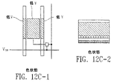
図1のEPDは、アップ/ダウンスイッチングモードのみを有する。図中のセルには、着色された(赤、緑および青)誘電性流体に正電荷を帯びた白色粒子が分散している懸濁液が充填されている。図1に、上部電極と底部電極(または下部電極)(図示せず)との間の電圧差によって帯電された全3つのセルを示す。緑および青のセルでは、上部電極が低電圧を有し、これら2つのセル内の正電荷を帯びた白色粒子は透明な上部表示電極へ移動し、結果として、粒子の色(即ち、白)が2つのセル内の透明導体フィルムを通って観察者に反射される。赤のセルでは、底部電極が低電圧を有する;その結果として、正電荷を帯びた白色粒子はセルの下部に移動し、媒体の色(即ち、赤)が上部の透明導体フィルムを通して見られる。図1に示すシナリオでは、緑および青のピクセルから反射される白色光が赤のピクセルの彩度を大きく下げる。
図2A−2Dに、インプレーンスイッチングモードのみを有する従来技術のEPDの不利点を示す。
図3は、本発明の典型的な電気泳動セルの側面図を示す。カップ状のセルのみが示されているが、本発明の範囲は、マイクロチャネルおよび同等のものから形成されたセルおよび全てのタイプの常套の電気泳動セルを包含すると理解されよう。
米国出願第09/518488号(2000年3月3日出願)および米国出願第09/784972号(2001年2月15日出願)に開示されているように、通常は、マイクロカップをマイクロエンボス加工またはフォトリソグラフィによって製造することができる。
雄型の製造
雄型は、例えば、ダイヤモンドターンプロセス(diamond turn process)またはレジストの現像後にエッチングもしくは電気メッキのいずれかを行うフォトレジストプロセス等のいずれの適当な方法によっても製造することができる。雄型用のマスターテンプレートは、電気メッキ等のいずれの適当な方法によっても製造することができる。電気メッキにより、ガラス基板にクロムインコネル等のシードメタルの薄層(典型的には3000Å)をスパッタする。次いで、フォトレジスト層をコートして、UVに曝露する。UVとフォトレジスト層との間にマスクを置く。フォトレジストの露光領域は硬化状態となる。次いで、非露光領域を、適当な溶媒を用いて洗浄することにより除去する。残りの硬化フォトレジストを乾燥させ、シードメタルの薄層を再びスパッタする。これにより、電鋳用のマスターの準備が完了する。電鋳用の典型的な材料は、ニッケルコバルトである。別法では、マスターを、「コンティニュアス・マニュファクチャリング・オブ・シン・カバー・シート・オプティカル・メディア(Continuous manufacturing of thin cover sheet optical media)」(SPIE Proc.)第1663巻、第324頁(1992年)に記載されているように無電解ニッケル付着または電鋳によりニッケルから形成してよい。型のフロアは、典型的には約50〜400ミクロンの厚さである。マスターは、e(電子)−ビーム・ライティング、ドライ・エッチング、ケミカル・エッチング、レーザー・ライティングまたはレーザー干渉(laser interference)(例えば「リプリケーション・テクニクス・フォー・マイクロ−オプティックス(Replication techniques for micro-optics)」(SPIE Proc.)第3099巻、第76〜82頁(1997年)に記載されているようなもの)を含む他のマイクロエンジニアリング技術を用いて製造することもできる。別法では、型は、プラスチック、セラミックまたは金属を用いるフォトマシニングまたはダイヤモンドターニングによって製造することができる。
マイクロカップアレイを製造するためのフォトリソグラフィ・プロセスを、図5Aおよび5Bに示す。
一態様において、マイクロカップの仕切壁は好ましくは不透明である(白色不透明または灰色不透明)。図13Aおよび13Bは、透明または不透明な仕切壁をそれぞれ有するマイクロカップの簡単な断面図を示す。図13Aは、2つのマイクロカップに分割する透明な仕切壁を通して、1つのマイクロカップ内の電気泳動組成物を、隣接するマイクロカップの上から見ることができることを示す。このような場合では、観察者は1色より多くの色を知覚することができ、結果としてカラーシフトまたはパララックス(ダブルイメージ)をもたらす。図13Bに示すように、仕切壁が不透明であると、この現象を避けることができる。不透明な仕切壁は、上述のマクロカップの形成のための放射線硬化性材料に、フィラー材料(例えば、シリカ、ZnO、TiO2、BaSO4、CaCO3またはポリマー粒子、好ましくはシリカまたはポリマー粒子)を1−20重量%の量、好ましくは2−10重量%の量で加えることによって得ることができる。
セルには、着色された誘電性溶媒中に分散する帯電色素粒子を含んで成る電気泳動組成物が充填されている。電気泳動組成物は、電界で移動しない付加的な着色剤をオプションとして含んでよい。色素分散物は、例えば米国特許第6017584号、第5914806号、第5573711号、第5403518号、第5380362号、第4680103号、第4285801号、第4093534号、第4071430号および第3668106号等の、当該技術分野で周知の方法によって調製してよい。また、アイ・イー・イー・イー・トランス・エレクトロン・デバイシィーズ(IEEE Trans. Electr. Dev.)、24巻、第827頁(1977年)、およびジャーナル・アプライド・フィジックス(J. Appl. Phys.)第49(9)巻、第4820頁(1978年)を参照のこと。
着色色素粒子を用いるとき、これらを、フタロシアニン・ブルー(phthalocyanine blue)、フタロシアニン・グリーン(phthalocyanine green)、ジアリリド・イェロー(diarylide yellow)、ジアリリド(diarylide)AAOTイェロー(yellow)、およびキナクリドン(quinacridone)、アゾ(azo)、ローダミン(rhodamine)、ペリレン(perylene)色素シリーズ(サン・ケミカル(Sun Chemical)製)、ハンサ・イェロー(Hansa yellow)Gパーティクルズ(particles)(関東化学製)、およびカーボン・ランプブラック(Carbon Lampblack)(フィッシャー(Fisher)製)から選択してよい。粒径は、好ましくは0.01−5ミクロンの範囲、更により好ましくは0.05−2ミクロンの範囲である。粒子は、許容できる光学特性を有する必要があり、誘電性溶媒によって膨潤または軟化してはならず、また、化学的に安定である必要がある。また、得られる懸濁液が、通常の操作条件において、沈降、クリーミングまたは凝集に対して安定であることも必要である。
充填およびシーリング方法は、同時係属特許出願である、米国出願第09/518488号、米国出願第09/784972号、米国出願第09/879408号、米国出願第09/874391号および米国出願第60/408256号(これらの開示内容は、全て、参照することにより本明細書に組み込まれる)に記載されている。
次いで、好ましくは接着層を有する別の電極フィルムを用いて、トップシールされたマイクロカップをラミネートする。適当な接着材料として、感圧性接着剤(アクリル系およびゴムタイプ)、UV硬化性接着剤(例えば、多官能性アクリレート、エポキシド、ビニルエーテルもしくはチオレン等を含む)、ならびに湿気または熱硬化性接着剤(例えば、エポキシ、ポリウレタンおよびシアノアクリレート等)が挙げられる。
上部基板層に上部電極層をコートまたはラミネートすることもできる。
表示側が、マイクロカップのトップシーリング側からであるとき、ブラックマトリクスを、図14Aに示すように仕切壁(141)の上面(140)とトップシーリング層(142)との間、図14Bに示すようにトップシーリング層(142)と(もし存在するならば)接着層(143)との間、図14Cに示すように(もし存在するならば)接着層(143)と上部電極層(144)との間、図14Dに示すように上部電極層(144)と上部基板(145)との間、または図14Eに示すように上部基板(145)の上部に適用することができる。表示側が底部からであるとき、ブラックマトリクスを、図14Fに示すようにマイクロカップ(146)と底部電極層(147)との間、図14Gに示すように底部電極層(147)と底部基板(148)との間、または図14Hに示すように底部基板(148)の底面に適用することができる。
IV(a) パッシブマトリクス
(1) 電極回路設計
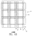
図6Aは、2層のパッシブマトリクス電極回路設計の側面図である。図6Bは、デュアルモードの2層のパッシブマトリクス電極設計の上面図を示す。1つの上部層(61)と底部層(62)との間にセル(60)をはさむ。水平方向のバーは、透明であり、且つセルの上部を走る行(ロウ)電極(63)である。底部層(62)は、セルの左側にある1つのインプレーン電極(64)、1つの底部列(カラム)電極(65)および右側の別のインプレーン電極(66)から成る。インプレーン電極とカラム電極との間にギャップ(67)が存在する。
本発明のデュアルモードスイッチングを説明するために、共通の黒背景および透明な(clear)着色溶媒中に分散する正電荷を帯びた白色粒子を含んで成る電気泳動セルを用いる。
(1) 電極回路設計
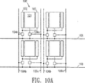
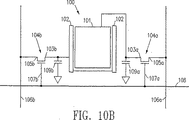
LCDディスプレイシステムに用いられるTFT(薄膜トランジスタ)アクティブマトリクス(Active Matrix)は、米国特許第5132820号に記載されている。そのようなTFT技術を、本発明のデュアルモードEPDに適用することもできる。好ましい態様では、例えばITO等の透明導体材料でできている上部層電極は、ディスプレイの上面全体を覆うワンピース形状である。上部電極はグラウンド(0V)に接続する。図10Aは、2x2のセルアレイの底部電極層の上面図を示す。図10Bは、TFT接続の詳細を示す。各セル(100)は、1つの底部電極(101)および2つのインプレーン電極(102)を含んで成る。各々の底部電極はTFT(104a)のドレイン(103a)に接続する。各セルのインプレーン電極は別のTFT(104b)のドレイン(103b)に接続する。TFT(104aおよび104b)のソース(105aおよび105b)は、デバイスの底面を通って垂直に走る信号線(106aおよび106b)に接続する。TFT(104aおよび104b)のゲート(107aおよび107b)は走査線(108)に接続し、該走査線はデバイスの底面を通って水平に走る。走査線および信号線はマトリクス構造を形成するが、互いに絶縁されている。
本発明のデュアルモードスイッチングを説明するために、共通の黒背景および透明な着色溶媒中に分散する正電荷を帯びた白色粒子を含んで成る電気泳動セルを用いる。
(1) 電極回路設計
この新規の設計では、駆動電極設計にパッシブマトリクス電極およびTFTアクティブマトリクスの両方を利用する。図11Aは駆動回路設計の上面図、図11Bはその側面図を示す。底部電極層(117)は、底部列電極(111)およびインプレーン電極(112)を含んで成る。各セルのインプレーン電極をTFT(113)のドレインに接続する。TFTのソースを、デバイスの底面を通って垂直に走る信号線(114)に接続する。TFTのゲートを、デバイスの底面を通って水平に走る走査線(115)に接続する。走査線および信号線はマトリクス構造を形成するが、2つのタイプの線は互いに絶縁されている。セル(110)を、1つの上部層(116)と底部層(117)との間に挟む。水平方向のバーは、透明であり且つセル(110)の上部を通って走る上部行電極(118)である。2つのインプレーン電極(112)と列電極(111)とを分離するギャップ(119)が存在する。上部行電極、底部列電極およびインプレーン電極の断面がディスプレイセルを規定する。
本発明のデュアルモードスイッチングを説明するために、共通の黒背景および透明な着色溶媒中に分散する正電荷を帯びた白色粒子を含んで成る電気泳動セルを用いる。
(1) 電極回路設計
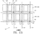
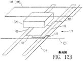
別の新規の設計では、駆動電極設計にパッシブマトリクス電極およびTFTアクティブマトリクスの両方を利用する。図12Aは、駆動回路設計の上面図を示し、図12Bはその側面図を示す。底部電極層(127)は、底部列電極(121)およびインプレーン電極(122)を含んで成る。各セルの底部電極をTFT(123)のドレインに接続する。TFTのソースを、デバイスの底面を通って垂直に走る信号線(124)に接続する。TFTのゲートを、デバイスの底面を通って水平に走る走査線(125)に接続する。走査線および信号線はマトリクス構造を形成するが、互いに絶縁されている。セル(120)を、上部層(126)と底部層(127)との間に挟む。水平方向のバーは、透明であり且つセルの上部を通って走る上部行電極(128)である。2つのインプレーン電極(122)と底部電極(121)とを分離するギャップ(129)が存在する。上部行電極、底部電極およびインプレーン電極の断面がディスプレイセルを規定する。
本発明のデュアルモードスイッチングを説明するために、共通の黒背景および透明な着色溶媒中に分散する正電荷を帯びた白色粒子を含んで成る電気泳動セルを用いる。
本願発明は以下の態様を含む。
(態様1)
電気泳動ディスプレイであって、
a) 上部電極を含んで成る上部層、
b) 底部電極および少なくとも1つのインプレーン電極を含んで成る底部層、ならびに
c) 上部層と底部層との間に挟まれた電気泳動セルのアレイ
を含んで成り、各々のセルは、
(i) 不透明な仕切壁、
(ii) セル背景、
(iii) セル内に充填された電気泳動組成物であって、着色された誘電性溶媒または溶媒混合物に分散された唯1種類の帯電色素粒子を含んで成る組成物
を含んで成る、電気泳動ディスプレイ。
(態様2)
不透明な仕切壁は白色である、態様1に記載の電気泳動ディスプレイ。
(態様3)
不透明な仕切壁は灰色である、態様1に記載の電気泳動ディスプレイ。
(態様4)
不透明な仕切壁は、UV硬化性材料およびフィラー、染料または色素を含んで成る組成物から形成されている、態様1に記載の電気泳動ディスプレイ。
(態様5)
フィラーは、シリカ、ZnO、TiO2、BaSO4、CaCO3およびポリマー粒子から成る群から選択される、態様4に記載の電気泳動ディスプレイ。
(態様6)
フィラー材料は、シリカまたはポリマー粒子である、態様4に記載の電気泳動ディスプレイ。
(態様7)
フィラー材料は、組成物の1−20重量%の量である、態様4に記載の電気泳動ディスプレイ。
(態様8)
フィラー材料は、組成物の2−10重量%の量である、態様7に記載の電気泳動ディスプレイ。
(態様9)
不透明な仕切壁は、放射線硬化性材料および潜在性光散乱材料を含んで成る組成物から形成されている、態様1に記載の電気泳動ディスプレイ。
(態様10)
潜在性光散乱材料は、硬化前には放射線硬化性材料に相溶性であるが、硬化後には非相溶性となる材料である、態様9に記載の電気泳動ディスプレイ。
(態様11)
潜在性光散乱材料は、熱的または光化学的なトリガーによってガスを放出する材料である、態様9に記載の電気泳動ディスプレイ。
(態様12)
熱的または光化学的なトリガーによってガスを放出する材料は、CO2を生成するカルボン酸、二環式のラクトンもしくは複素環化合物;COを生成するケトンもしくは二環式の付加化合物;SOおよびSO2を生成するスルホン、スルホニルオキシ化合物もしくは複素環化合物;N2を生成するアゾアルカン、アジド、ジアゾメタン、N−ニトロソ化合物、ジアゾ、トリアゾもしくはテトラアゾ複素環化合物;COSを生成するキサンテートならびにO2を生成するエンドペルオキシドから成る群から選択される、態様11に記載の電気泳動ディスプレイ。
(態様13)
熱的または光化学的なトリガーによってガスを放出する材料は、フェノール、トロポロン、ピリジン、ピラジン、ピロールまたはこれらのハロゲン化誘導体である、態様11に記載の電気泳動ディスプレイ。
(態様14)
不透明な仕切壁は、着色されている、態様1に記載の電気泳動ディスプレイ。
(態様15)
仕切壁の内面は、電気泳動組成物と同じ色を有する、態様1に記載の電気泳動ディスプレイ。
(態様16)
仕切壁の2つの側面は、異なる色を有する、態様15に記載の電気泳動ディスプレイ。
(態様17)
電気泳動ディスプレイであって
a) 上部電極層およびオプションとしての上部基板を含んで成る上部層、
b) 底部電極層およびオプションとしての底部基板を含んで成る底部層であって、底部電極層が1つの底部電極および少なくとも1つのインプレーン電極を含んで成る底部層、ならびに
c) 上部層と底部層との間に挟まれた電気泳動セルのアレイ
を含んで成り、各々のセルは、
(i) 上面を有する仕切壁、
(ii) 仕切壁の上面または別の層の仕切壁の上面に対応する領域にあるブラックマトリクス層、
(iii) セル背景、ならびに
(iv) セル内に充填された電気泳動組成物であって、着色された誘電性溶媒または溶媒混合物に分散された唯1種類の帯電色素粒子を含んで成る組成物
を含んで成る、電気泳動ディスプレイ。
(態様18)
ブラックマトリクス層は、仕切壁の上面にある、態様17に記載の電気泳動ディスプレイ。
(態様19)
各々の電気泳動セルは、各々のセルに電気泳動組成物を封入するトップシーリング層を含んで成る、態様17に記載の電気泳動ディスプレイ。
(態様20)
上部電極層は、接着層が適用されている、態様19に記載の電気泳動ディスプレイ。
(態様21)
ブラックマトリクス層は、トップシーリング層と接着層との間にある、態様20に記載の電気泳動ディスプレイ。
(態様22)
ブラックマトリクス層は、接着層と上部電極層との間にある、態様20に記載の電気泳動ディスプレイ。
(態様23)
ブラックマトリクス層は、上部電極層と上部基板との間にある、態様17に記載の電気泳動ディスプレイ。
(態様24)
ブラックマトリクス層は、上部基板の上にある、態様17に記載の電気泳動ディスプレイ。
(態様25)
ブラックマトリクス層は、電気泳動セルと底部電極層との間にある、態様17に記載の電気泳動ディスプレイ。
(態様26)
ブラックマトリクス層は、底部電極層と底部基板との間にある、態様17に記載の電気泳動ディスプレイ。
(態様27)
ブラックマトリクス層は、底部基板の底面にある、態様17に記載の電気泳動ディスプレイ。
(態様28)
ブラックマトリクス層は、仕切壁の上面に位置合わせをして適用されている、態様17に記載の電気泳動ディスプレイ。
(態様29)
ブラックマトリクス層は、印刷、スタンピングまたはフォトリソグラフィによって適用されている、態様17に記載の電気泳動ディスプレイ。
(態様30)
ブラックマトリクス層は、蒸着またはシャドウマスクを用いるスパッタリングによって適用されている、態様17に記載の電気泳動ディスプレイ。
(態様31)
ブラックマトリクス層の光学密度は、0.5より高い、態様17に記載の電気泳動ディスプレイ。
(態様32)
ブラックマトリクス層の光学密度は、1より高い、態様31に記載の電気泳動ディスプレイ。
(態様33)
ブラックマトリクス層の厚さは、0.005μm〜5μmの範囲内である、態様17に記載の電気泳動ディスプレイ。
(態様34)
ブラックマトリクス層の厚さは、0.01μm〜2μmの範囲内である、態様33に記載の電気泳動ディスプレイ。
(態様35)
ブラックマトリクス層の直接または間接的に上にあるディフューザー層を更に含んで成る、態様17に記載の電気泳動ディスプレイ。
(態様36)
ブラックマトリクス層は、高度に架橋されたブラックマトリクス層である、態様17に記載の電気泳動ディスプレイ。
(態様37)
帯電色素粒子は、色素含有マイクロ粒子である、態様1または17に記載の電気泳動ディスプレイ。
(態様38)
色素含有マイクロ粒子は、誘電性溶媒の比重に適合した比重を有する、態様37に記載の電気泳動ディスプレイ。
(態様39)
仕切壁は不透明である、態様17に記載の電気泳動ディスプレイ。
(態様40)
仕切壁は白色不透明である、態様39に記載の電気泳動ディスプレイ。
(態様41)
仕切壁は灰色不透明である、態様39に記載の電気泳動ディスプレイ。
(態様42)
仕切壁は着色されている、態様17に記載の電気泳動ディスプレイ。
(態様43)
仕切壁の内面は、電気泳動組成物と同じ色を有する、態様17に記載の電気泳動ディスプレイ。
(態様44)
仕切壁の2つの側面は異なる色を有する、態様43に記載の電気泳動ディスプレイ。
Claims (24)
- 電気泳動セルのアレイを含んで成る電気泳動ディスプレイであって、該電気泳動セルの各々が、
a) 上部電極を含んで成る上部層と、底部電極および少なくとも1つのインプレーン電極を含んで成る底部層との間に挟まれ、
b) 着色された誘電性溶媒または溶媒混合物に分散された帯電色素粒子を含んで成る電気泳動組成物により充填され、
c) 不透明な仕切壁およびセル背景を含んで成り、および
d) 色素粒子の色、着色された誘電性溶媒または溶媒混合物の色、またはセル背景の色である3種の色状態を表示可能である、電気泳動ディスプレイ。 - 帯電色素粒子は同じ色を有する、請求項1に記載の電気泳動ディスプレイ。
- 不透明な仕切壁は白色または灰色である、請求項1に記載の電気泳動ディスプレイ。
- 不透明な仕切壁は、UV硬化性材料およびフィラー、染料または色素を含んで成る組成物から形成されている、請求項1に記載の電気泳動ディスプレイ。
- 不透明な仕切壁は、放射線硬化性材料および潜在性光散乱材料を含んで成る組成物から形成されている、請求項1に記載の電気泳動ディスプレイ。
- 不透明な仕切壁は、着色されている、請求項1に記載の電気泳動ディスプレイ。
- 仕切壁の内面は、着色された誘電性溶媒または溶媒混合物と同じ色を有する、請求項1に記載の電気泳動ディスプレイ。
- 仕切壁の2つの側面は、異なる色を有する、請求項7に記載の電気泳動ディスプレイ。
- 電気泳動セルのアレイを含んで成る電気泳動ディスプレイであって、該電気泳動セルの各々が、
a) 上部電極を含んで成る上部層と、底部電極および少なくとも1つのインプレーン電極を含んで成る底部層との間に挟まれ、
b) 着色された誘電性溶媒または溶媒混合物に分散された帯電色素粒子を含んで成る電気泳動組成物により充填され、
c) セル背景、上面を有する仕切壁、および仕切壁の上面に対して位置合わせされたブラックマトリクス層を含んで成り、および
d) 色素粒子の色、着色された誘電性溶媒または溶媒混合物の色、またはセル背景の色である3種の色状態を表示可能である、電気泳動ディスプレイ。 - 帯電色素粒子は同じ色を有する、請求項9に記載の電気泳動ディスプレイ。
- ブラックマトリクス層は、仕切壁の上面にある、請求項9に記載の電気泳動ディスプレイ。
- ブラックマトリクス層は、トップシーリング層と接着層との間にある、請求項9に記載の電気泳動ディスプレイ。
- ブラックマトリクス層は、接着層と、前記上部電極を含んで成る上部電極層との間にある、請求項9に記載の電気泳動ディスプレイ。
- ブラックマトリクス層は、前記上部電極を含んで成る上部電極層と、上部基板との間にある、請求項9に記載の電気泳動ディスプレイ。
- ブラックマトリクス層は、上部基板の上にある、請求項9に記載の電気泳動ディスプレイ。
- ブラックマトリクス層は、電気泳動セルと、前記底部電極を含んで成る底部電極層との間にある、請求項9に記載の電気泳動ディスプレイ。
- ブラックマトリクス層は、前記底部電極を含んで成る底部電極層と、底部基板との間にある、請求項9に記載の電気泳動ディスプレイ。
- ブラックマトリクス層は、底部基板の底面にある、請求項9に記載の電気泳動ディスプレイ。
- ブラックマトリクス層の直接または間接的に上にあるディフューザー層を更に含んで成る、請求項9に記載の電気泳動ディスプレイ。
- 色素粒子は、色素含有マイクロ粒子である、請求項1または9に記載の電気泳動ディスプレイ。
- 仕切壁は白色不透明または灰色不透明である、請求項9に記載の電気泳動ディスプレイ。
- 仕切壁は着色されている、請求項9に記載の電気泳動ディスプレイ。
- 仕切壁の内面は、着色された誘電性溶媒または溶媒混合物と同じ色を有する、請求項9に記載の電気泳動ディスプレイ。
- 仕切壁の2つの側面は異なる色を有する、請求項23に記載の電気泳動ディスプレイ。
Applications Claiming Priority (2)
| Application Number | Priority Date | Filing Date | Title |
|---|---|---|---|
| US10/367,098 US7038670B2 (en) | 2002-08-16 | 2003-02-14 | Electrophoretic display with dual mode switching |
| PCT/US2004/004835 WO2004074912A2 (en) | 2003-02-14 | 2004-02-13 | Electrophoretic display with dual-mode switching |
Publications (3)
| Publication Number | Publication Date |
|---|---|
| JP2006518052A JP2006518052A (ja) | 2006-08-03 |
| JP2006518052A5 JP2006518052A5 (ja) | 2007-04-05 |
| JP4598759B2 true JP4598759B2 (ja) | 2010-12-15 |
Family
ID=32907618
Family Applications (1)
| Application Number | Title | Priority Date | Filing Date |
|---|---|---|---|
| JP2006503689A Expired - Lifetime JP4598759B2 (ja) | 2003-02-14 | 2004-02-13 | デュアルモードスイッチングを有する電気泳動ディスプレイ |
Country Status (5)
| Country | Link |
|---|---|
| US (2) | US7038670B2 (ja) |
| JP (1) | JP4598759B2 (ja) |
| CN (1) | CN1275087C (ja) |
| TW (1) | TWI260460B (ja) |
| WO (1) | WO2004074912A2 (ja) |
Families Citing this family (138)
| Publication number | Priority date | Publication date | Assignee | Title |
|---|---|---|---|---|
| US7956841B2 (en) * | 1995-07-20 | 2011-06-07 | E Ink Corporation | Stylus-based addressing structures for displays |
| US7715088B2 (en) * | 2000-03-03 | 2010-05-11 | Sipix Imaging, Inc. | Electrophoretic display |
| US7038670B2 (en) | 2002-08-16 | 2006-05-02 | Sipix Imaging, Inc. | Electrophoretic display with dual mode switching |
| US7492505B2 (en) | 2001-08-17 | 2009-02-17 | Sipix Imaging, Inc. | Electrophoretic display with dual mode switching |
| TW550529B (en) | 2001-08-17 | 2003-09-01 | Sipix Imaging Inc | An improved electrophoretic display with dual-mode switching |
| JP2004271610A (ja) * | 2003-03-05 | 2004-09-30 | Canon Inc | カラー電気泳動表示装置 |
| JP2004286861A (ja) * | 2003-03-19 | 2004-10-14 | Canon Inc | 電気泳動表示装置の製造方法 |
| US7173752B2 (en) * | 2003-11-05 | 2007-02-06 | E Ink Corporation | Electro-optic displays, and materials for use therein |
| US20110164301A1 (en) | 2003-11-05 | 2011-07-07 | E Ink Corporation | Electro-optic displays, and materials for use therein |
| JP2005266613A (ja) * | 2004-03-19 | 2005-09-29 | Canon Inc | 粒子移動型表示装置 |
| US7126621B2 (en) * | 2004-07-30 | 2006-10-24 | Xerox Corporation | Printer using hybrid reflex writing to color register an image |
| TWI454787B (zh) * | 2005-04-08 | 2014-10-01 | Sipix Imaging Inc | 反射式顯示器及其製造方法 |
| KR100631291B1 (ko) * | 2005-04-08 | 2006-10-04 | 주식회사 동진쎄미켐 | 전계 구동 반사형 표시 장치 |
| US8159636B2 (en) * | 2005-04-08 | 2012-04-17 | Sipix Imaging, Inc. | Reflective displays and processes for their manufacture |
| EP1770672A1 (en) * | 2005-09-28 | 2007-04-04 | Samsung SDI Co., Ltd. | Flat panel display and a method of driving the same |
| CN101288023A (zh) * | 2005-10-14 | 2008-10-15 | 皇家飞利浦电子股份有限公司 | 平面内切换显示设备 |
| JP2007171890A (ja) * | 2005-11-22 | 2007-07-05 | Bridgestone Corp | 情報表示用パネル |
| KR20080077628A (ko) * | 2005-12-20 | 2008-08-25 | 코닌클리케 필립스 일렉트로닉스 엔.브이. | 개선된 평면 내 스위칭 전기영동 디스플레이 |
| US7479968B2 (en) * | 2006-01-31 | 2009-01-20 | Microsoft Corporation | Semi-transparent highlighting of selected objects in electronic documents |
| US7982479B2 (en) * | 2006-04-07 | 2011-07-19 | Sipix Imaging, Inc. | Inspection methods for defects in electrophoretic display and related devices |
| KR20080010144A (ko) * | 2006-07-26 | 2008-01-30 | 삼성전자주식회사 | 전기영동 표시장치 |
| CN101206373A (zh) * | 2006-12-20 | 2008-06-25 | 启萌科技有限公司 | 显示装置及其制造方法 |
| JP5157322B2 (ja) * | 2007-08-30 | 2013-03-06 | セイコーエプソン株式会社 | 電気泳動表示装置、電気泳動表示装置の駆動方法、及び電子機器 |
| JP5478817B2 (ja) * | 2007-08-30 | 2014-04-23 | 株式会社ジャパンディスプレイ | 液晶表示装置およびその製造方法 |
| EP2198326B1 (en) * | 2007-09-21 | 2014-05-07 | LG Display Co., Ltd. | Color filter, method of fabricating the same and display device |
| US8169690B2 (en) * | 2008-02-21 | 2012-05-01 | Sipix Imaging, Inc. | Color display devices |
| CN102177463B (zh) | 2008-04-03 | 2015-04-22 | 希毕克斯影像有限公司 | 彩色显示设备 |
| US8072675B2 (en) * | 2008-05-01 | 2011-12-06 | Sipix Imaging, Inc. | Color display devices |
| EP2172804B1 (en) | 2008-10-03 | 2016-05-11 | Semiconductor Energy Laboratory Co, Ltd. | Display device |
| US8466879B2 (en) | 2008-10-26 | 2013-06-18 | Microsoft Corporation | Multi-touch manipulation of application objects |
| US8477103B2 (en) | 2008-10-26 | 2013-07-02 | Microsoft Corporation | Multi-touch object inertia simulation |
| US8503063B2 (en) * | 2008-12-30 | 2013-08-06 | Sipix Imaging, Inc. | Multicolor display architecture using enhanced dark state |
| US8797258B2 (en) * | 2008-12-30 | 2014-08-05 | Sipix Imaging, Inc. | Highlight color display architecture using enhanced dark state |
| US8717664B2 (en) | 2012-10-02 | 2014-05-06 | Sipix Imaging, Inc. | Color display device |
| US8964282B2 (en) * | 2012-10-02 | 2015-02-24 | E Ink California, Llc | Color display device |
| JP4930561B2 (ja) * | 2009-09-07 | 2012-05-16 | カシオ計算機株式会社 | 電気泳動表示パネル |
| US9390661B2 (en) | 2009-09-15 | 2016-07-12 | E Ink California, Llc | Display controller system |
| CN102033383A (zh) * | 2009-09-24 | 2011-04-27 | 鸿富锦精密工业(深圳)有限公司 | 电子纸装置 |
| US20110217639A1 (en) * | 2010-03-02 | 2011-09-08 | Sprague Robert A | Electrophoretic display fluid |
| JP2011237771A (ja) * | 2010-04-12 | 2011-11-24 | Seiko Epson Corp | 電気泳動表示装置および電子機器 |
| JP2011237770A (ja) | 2010-04-12 | 2011-11-24 | Seiko Epson Corp | 電気泳動表示装置およびその駆動方法、電子機器 |
| US9140952B2 (en) | 2010-04-22 | 2015-09-22 | E Ink California, Llc | Electrophoretic display with enhanced contrast |
| US9087801B2 (en) * | 2010-04-29 | 2015-07-21 | Apple Inc. | Power efficient organic light emitting diode display |
| KR101343800B1 (ko) * | 2010-05-10 | 2013-12-20 | 엘지디스플레이 주식회사 | 전기 영동 디스플레이 장치 및 그 제조 방법 |
| US8120838B2 (en) * | 2010-05-19 | 2012-02-21 | Au Optronics Corporation | Electrophoretic display device |
| US8704756B2 (en) | 2010-05-26 | 2014-04-22 | Sipix Imaging, Inc. | Color display architecture and driving methods |
| US20130141780A1 (en) * | 2010-08-09 | 2013-06-06 | Yoocharn Jeon | System And Method For Tri-state Electro-optical Displays |
| KR20120022253A (ko) * | 2010-09-01 | 2012-03-12 | 엘지디스플레이 주식회사 | 전기영동 표시소자 및 그 제조방법 |
| KR20120026302A (ko) * | 2010-09-09 | 2012-03-19 | 삼성전기주식회사 | 전자종이 표시소자 및 그 제조방법 |
| US20130208345A1 (en) * | 2010-09-30 | 2013-08-15 | Kolon Industries, Inc. | Electrophoresis display device and preparation method of the same |
| US8670174B2 (en) | 2010-11-30 | 2014-03-11 | Sipix Imaging, Inc. | Electrophoretic display fluid |
| KR101759643B1 (ko) * | 2010-12-17 | 2017-08-01 | 삼성디스플레이 주식회사 | 전기영동 표시장치 |
| US10514583B2 (en) | 2011-01-31 | 2019-12-24 | E Ink California, Llc | Color electrophoretic display |
| US9146439B2 (en) | 2011-01-31 | 2015-09-29 | E Ink California, Llc | Color electrophoretic display |
| US8786935B2 (en) | 2011-06-02 | 2014-07-22 | Sipix Imaging, Inc. | Color electrophoretic display |
| US9013783B2 (en) | 2011-06-02 | 2015-04-21 | E Ink California, Llc | Color electrophoretic display |
| JP5556762B2 (ja) * | 2011-08-01 | 2014-07-23 | 日立化成株式会社 | 懸濁粒子装置,懸濁粒子装置を用いた調光装置及びそれらの駆動方法 |
| US8605354B2 (en) | 2011-09-02 | 2013-12-10 | Sipix Imaging, Inc. | Color display devices |
| US8649084B2 (en) | 2011-09-02 | 2014-02-11 | Sipix Imaging, Inc. | Color display devices |
| US20140367622A1 (en) * | 2012-01-27 | 2014-12-18 | Applied Nanotech Holdings, Inc. | Display medium and color reflective inks |
| US8917439B2 (en) | 2012-02-09 | 2014-12-23 | E Ink California, Llc | Shutter mode for color display devices |
| US8797636B2 (en) | 2012-07-17 | 2014-08-05 | Sipix Imaging, Inc. | Light-enhancing structure for electrophoretic display |
| US11017705B2 (en) | 2012-10-02 | 2021-05-25 | E Ink California, Llc | Color display device including multiple pixels for driving three-particle electrophoretic media |
| US9360733B2 (en) | 2012-10-02 | 2016-06-07 | E Ink California, Llc | Color display device |
| TWI503808B (zh) | 2013-05-17 | 2015-10-11 | 希畢克斯幻像有限公司 | 用於彩色顯示裝置之驅動方法 |
| TWI550332B (zh) | 2013-10-07 | 2016-09-21 | 電子墨水加利福尼亞有限責任公司 | 用於彩色顯示裝置的驅動方法 |
| US10380931B2 (en) | 2013-10-07 | 2019-08-13 | E Ink California, Llc | Driving methods for color display device |
| US10726760B2 (en) | 2013-10-07 | 2020-07-28 | E Ink California, Llc | Driving methods to produce a mixed color state for an electrophoretic display |
| TWI534520B (zh) | 2013-10-11 | 2016-05-21 | 電子墨水加利福尼亞有限責任公司 | 彩色顯示裝置 |
| JP6441369B2 (ja) | 2014-01-14 | 2018-12-19 | イー インク カリフォルニア, エルエルシー | フルカラーディスプレイデバイス |
| US9541814B2 (en) | 2014-02-19 | 2017-01-10 | E Ink California, Llc | Color display device |
| WO2015172813A1 (en) | 2014-05-13 | 2015-11-19 | Visitret Displays Ltd. | Electrophoretic display panel structure and its manufacturing process |
| US10891906B2 (en) | 2014-07-09 | 2021-01-12 | E Ink California, Llc | Color display device and driving methods therefor |
| US10380955B2 (en) | 2014-07-09 | 2019-08-13 | E Ink California, Llc | Color display device and driving methods therefor |
| US9922603B2 (en) | 2014-07-09 | 2018-03-20 | E Ink California, Llc | Color display device and driving methods therefor |
| PL3167337T3 (pl) | 2014-07-09 | 2022-07-25 | E Ink California, Llc | Sposób sterowania kolorowym urządzeniem elektroforetycznym |
| TWI623928B (zh) | 2015-02-04 | 2018-05-11 | 電子墨水股份有限公司 | 在深色模式及淺色模式中顯示之光電顯示器以及其相關裝置及方法 |
| US11087644B2 (en) | 2015-08-19 | 2021-08-10 | E Ink Corporation | Displays intended for use in architectural applications |
| EP3345047A1 (en) | 2015-08-31 | 2018-07-11 | E Ink Corporation | Electronically erasing a drawing device |
| EP3350798B1 (en) | 2015-09-16 | 2023-07-26 | E Ink Corporation | Apparatus and methods for driving displays |
| US10803813B2 (en) | 2015-09-16 | 2020-10-13 | E Ink Corporation | Apparatus and methods for driving displays |
| US11657774B2 (en) | 2015-09-16 | 2023-05-23 | E Ink Corporation | Apparatus and methods for driving displays |
| KR20180041768A (ko) | 2015-10-12 | 2018-04-24 | 이 잉크 캘리포니아 엘엘씨 | 전기영동 디스플레이 디바이스 |
| CN108351569B (zh) | 2015-11-18 | 2021-12-03 | 伊英克公司 | 电光显示器 |
| KR102243196B1 (ko) | 2016-02-19 | 2021-04-22 | 애버리 데니슨 코포레이션 | 접착제를 제조하는 2단계 방법 및 관련 조성물 |
| US10276109B2 (en) | 2016-03-09 | 2019-04-30 | E Ink Corporation | Method for driving electro-optic displays |
| US10593272B2 (en) | 2016-03-09 | 2020-03-17 | E Ink Corporation | Drivers providing DC-balanced refresh sequences for color electrophoretic displays |
| CN112331122B (zh) | 2016-05-24 | 2023-11-07 | 伊英克公司 | 用于渲染彩色图像的方法 |
| US10640595B2 (en) | 2016-10-25 | 2020-05-05 | Avery Dennison Corporation | Controlled architecture polymerization with photoinitiator groups in backbone |
| JP7139335B2 (ja) | 2017-01-20 | 2022-09-20 | イー インク カリフォルニア, エルエルシー | 着色有機顔料およびこれを含む電気泳動ディスプレイ媒体 |
| CA3050122C (en) | 2017-03-06 | 2020-07-28 | E Ink Corporation | Method and apparatus for rendering color images |
| KR102531228B1 (ko) | 2017-04-04 | 2023-05-10 | 이 잉크 코포레이션 | 전기 광학 디스플레이들을 구동하기 위한 방법들 |
| US11404013B2 (en) | 2017-05-30 | 2022-08-02 | E Ink Corporation | Electro-optic displays with resistors for discharging remnant charges |
| WO2018222638A1 (en) | 2017-05-30 | 2018-12-06 | E Ink Corporation | Electro-optic displays |
| US11721295B2 (en) | 2017-09-12 | 2023-08-08 | E Ink Corporation | Electro-optic displays, and methods for driving same |
| CN111133501A (zh) | 2017-09-12 | 2020-05-08 | 伊英克公司 | 用于驱动电光显示器的方法 |
| TWI744848B (zh) | 2017-10-18 | 2021-11-01 | 英商核酸有限公司 | 包含具薄膜電晶體及電容感測之雙基板的數位微流體裝置 |
| JP6972334B2 (ja) | 2017-11-14 | 2021-11-24 | イー インク カリフォルニア, エルエルシー | 多孔性伝導電極層を含む電気泳動活性分子送達システム |
| US11079651B2 (en) | 2017-12-15 | 2021-08-03 | E Ink Corporation | Multi-color electro-optic media |
| CN111492307A (zh) | 2017-12-19 | 2020-08-04 | 伊英克公司 | 电光显示器的应用 |
| US11248122B2 (en) | 2017-12-30 | 2022-02-15 | E Ink Corporation | Pigments for electrophoretic displays |
| JP2021511542A (ja) | 2018-01-22 | 2021-05-06 | イー インク コーポレイション | 電気光学ディスプレイおよびそれらを駆動する方法 |
| US11143929B2 (en) | 2018-03-09 | 2021-10-12 | E Ink Corporation | Reflective electrophoretic displays including photo-luminescent material and color filter arrays |
| CA3105173C (en) | 2018-07-17 | 2023-05-23 | E Ink California, Llc | Electro-optic displays and driving methods |
| CN112470067A (zh) | 2018-08-10 | 2021-03-09 | 伊英克加利福尼亚有限责任公司 | 具有反射器的可切换的光准直层 |
| CN112470066A (zh) | 2018-08-10 | 2021-03-09 | 伊英克加利福尼亚有限责任公司 | 用于包括双稳态电泳流体的可切换的光准直层的驱动波形 |
| US11397366B2 (en) | 2018-08-10 | 2022-07-26 | E Ink California, Llc | Switchable light-collimating layer including bistable electrophoretic fluid |
| US11353759B2 (en) | 2018-09-17 | 2022-06-07 | Nuclera Nucleics Ltd. | Backplanes with hexagonal and triangular electrodes |
| CN108957899B (zh) * | 2018-09-25 | 2023-06-06 | 无锡威峰科技股份有限公司 | 一种双层微结构的显示电浆模组及其制造方法 |
| WO2020081478A1 (en) | 2018-10-15 | 2020-04-23 | E Ink Corporation | Digital microfluidic delivery device |
| RU2760510C1 (ru) | 2018-11-30 | 2021-11-25 | Е Инк Калифорния, Ллс | Электрооптические дисплеи и способы их возбуждения |
| CN110520791B (zh) * | 2019-07-17 | 2023-09-05 | 京东方科技集团股份有限公司 | 显示基板及其驱动方法、显示装置 |
| CA3157990A1 (en) | 2019-11-14 | 2021-05-20 | E Ink Corporation | Methods for driving electro-optic displays |
| WO2021101859A1 (en) | 2019-11-18 | 2021-05-27 | E Ink Corporation | Methods for driving electro-optic displays |
| US11938214B2 (en) | 2019-11-27 | 2024-03-26 | E Ink Corporation | Benefit agent delivery system comprising microcells having an electrically eroding sealing layer |
| WO2021247450A1 (en) | 2020-05-31 | 2021-12-09 | E Ink Corporation | Electro-optic displays, and methods for driving same |
| JP2023527541A (ja) | 2020-06-05 | 2023-06-29 | イー インク カリフォルニア, エルエルシー | 電気泳動ディスプレイデバイス |
| US11520202B2 (en) | 2020-06-11 | 2022-12-06 | E Ink Corporation | Electro-optic displays, and methods for driving same |
| US11846863B2 (en) | 2020-09-15 | 2023-12-19 | E Ink Corporation | Coordinated top electrode—drive electrode voltages for switching optical state of electrophoretic displays using positive and negative voltages of different magnitudes |
| AU2021344334B2 (en) | 2020-09-15 | 2023-12-07 | E Ink Corporation | Improved driving voltages for advanced color electrophoretic displays and displays with improved driving voltages |
| EP4214574A1 (en) | 2020-09-15 | 2023-07-26 | E Ink Corporation | Four particle electrophoretic medium providing fast, high-contrast optical state switching |
| WO2022072596A1 (en) | 2020-10-01 | 2022-04-07 | E Ink Corporation | Electro-optic displays, and methods for driving same |
| US11721296B2 (en) | 2020-11-02 | 2023-08-08 | E Ink Corporation | Method and apparatus for rendering color images |
| AU2021368779B2 (en) | 2020-11-02 | 2024-03-07 | E Ink Corporation | Enhanced push-pull (EPP) waveforms for achieving primary color sets in multi-color electrophoretic displays |
| US11756494B2 (en) | 2020-11-02 | 2023-09-12 | E Ink Corporation | Driving sequences to remove prior state information from color electrophoretic displays |
| US11657772B2 (en) | 2020-12-08 | 2023-05-23 | E Ink Corporation | Methods for driving electro-optic displays |
| WO2023023213A1 (en) | 2021-08-18 | 2023-02-23 | E Ink Corporation | Methods for driving electro-optic displays |
| WO2023034683A1 (en) | 2021-09-06 | 2023-03-09 | E Ink California, Llc | Method for driving electrophoretic display device |
| WO2023043714A1 (en) | 2021-09-14 | 2023-03-23 | E Ink Corporation | Coordinated top electrode - drive electrode voltages for switching optical state of electrophoretic displays using positive and negative voltages of different magnitudes |
| US11830448B2 (en) | 2021-11-04 | 2023-11-28 | E Ink Corporation | Methods for driving electro-optic displays |
| US11869451B2 (en) | 2021-11-05 | 2024-01-09 | E Ink Corporation | Multi-primary display mask-based dithering with low blooming sensitivity |
| WO2023121901A1 (en) | 2021-12-22 | 2023-06-29 | E Ink Corporation | High voltage driving using top plane switching with zero voltage frames between driving frames |
| US20230197024A1 (en) | 2021-12-22 | 2023-06-22 | E Ink Corporation | Methods for driving electro-optic displays |
| WO2023129533A1 (en) | 2021-12-27 | 2023-07-06 | E Ink Corporation | Methods for measuring electrical properties of electro-optic displays |
| US20230213832A1 (en) | 2021-12-30 | 2023-07-06 | E Ink California, Llc | Methods for driving electro-optic displays |
| WO2023132958A1 (en) | 2022-01-04 | 2023-07-13 | E Ink Corporation | Electrophoretic media comprising electrophoretic particles and a combination of charge control agents |
| WO2023211867A1 (en) | 2022-04-27 | 2023-11-02 | E Ink Corporation | Color displays configured to convert rgb image data for display on advanced color electronic paper |
| WO2024044119A1 (en) | 2022-08-25 | 2024-02-29 | E Ink Corporation | Transitional driving modes for impulse balancing when switching between global color mode and direct update mode for electrophoretic displays |
Family Cites Families (107)
| Publication number | Priority date | Publication date | Assignee | Title |
|---|---|---|---|---|
| US3892568A (en) | 1969-04-23 | 1975-07-01 | Matsushita Electric Ind Co Ltd | Electrophoretic image reproduction process |
| US3612758A (en) | 1969-10-03 | 1971-10-12 | Xerox Corp | Color display device |
| US3668106A (en) | 1970-04-09 | 1972-06-06 | Matsushita Electric Ind Co Ltd | Electrophoretic display device |
| US3697679A (en) | 1970-07-01 | 1972-10-10 | Ampex | Automatic threading video recorder |
| JPS5222236B2 (ja) | 1972-05-04 | 1977-06-16 | ||
| JPS5228555B2 (ja) | 1972-06-30 | 1977-07-27 | ||
| US4093534A (en) | 1974-02-12 | 1978-06-06 | Plessey Handel Und Investments Ag | Working fluids for electrophoretic image display devices |
| US4071430A (en) | 1976-12-06 | 1978-01-31 | North American Philips Corporation | Electrophoretic image display having an improved switching time |
| DE2906652A1 (de) | 1979-02-02 | 1980-08-14 | Bbc Brown Boveri & Cie | Verfahren zur herstellung einer elektrophoretischen anzeige mit wachsumhuellten pigmentteilchen |
| US4285801A (en) | 1979-09-20 | 1981-08-25 | Xerox Corporation | Electrophoretic display composition |
| JPS59171930A (ja) | 1983-03-18 | 1984-09-28 | Matsushita Electric Ind Co Ltd | 電気泳動表示素子 |
| US4741988A (en) | 1985-05-08 | 1988-05-03 | U.S. Philips Corp. | Patterned polyimide film, a photosensitive polyamide acid derivative and an electrophoretic image-display cell |
| US4680103A (en) | 1986-01-24 | 1987-07-14 | Epid. Inc. | Positive particles in electrophoretic display device composition |
| JP2620240B2 (ja) | 1987-06-10 | 1997-06-11 | 株式会社日立製作所 | 液晶表示装置 |
| JP2862571B2 (ja) * | 1988-07-28 | 1999-03-03 | 株式会社東芝 | 透過型液晶表示装置 |
| US5378574A (en) * | 1988-08-17 | 1995-01-03 | Xerox Corporation | Inks and liquid developers containing colored silica particles |
| US4995718A (en) | 1989-11-15 | 1991-02-26 | Honeywell Inc. | Full color three-dimensional projection display |
| US5326865A (en) | 1990-06-08 | 1994-07-05 | Hercules Incorporated | Arylazo and poly(arylazo) dyes having at least one core radical selected from naphthyl or anthracyl and having at least one 2,3-dihydro-1,3-dialkyl perimidine substituent |
| WO1993005425A1 (en) | 1991-08-29 | 1993-03-18 | Copytele, Inc. | Electrophoretic display panel with internal mesh background screen |
| US5279511A (en) | 1992-10-21 | 1994-01-18 | Copytele, Inc. | Method of filling an electrophoretic display |
| US5345251A (en) * | 1993-01-11 | 1994-09-06 | Copytele, Inc. | Electrophoretic display panel with interleaved cathode and anode |
| WO1994028202A1 (en) | 1993-05-21 | 1994-12-08 | Copytele, Inc. | Methods of preparing electrophoretic dispersions containing two types of particles with different colors and opposite charges |
| US5380362A (en) | 1993-07-16 | 1995-01-10 | Copytele, Inc. | Suspension for use in electrophoretic image display systems |
| US6111598A (en) | 1993-11-12 | 2000-08-29 | Peveo, Inc. | System and method for producing and displaying spectrally-multiplexed images of three-dimensional imagery for use in flicker-free stereoscopic viewing thereof |
| US5403518A (en) | 1993-12-02 | 1995-04-04 | Copytele, Inc. | Formulations for improved electrophoretic display suspensions and related methods |
| US5699097A (en) | 1994-04-22 | 1997-12-16 | Kabushiki Kaisha Toshiba | Display medium and method for display therewith |
| CA2191084A1 (en) | 1994-05-26 | 1995-12-07 | Wei-Hsin Hou | Fluorinated dielectric suspensions for electrophoretic image displays and related methods |
| US5745094A (en) * | 1994-12-28 | 1998-04-28 | International Business Machines Corporation | Electrophoretic display |
| US7259744B2 (en) | 1995-07-20 | 2007-08-21 | E Ink Corporation | Dielectrophoretic displays |
| US6120839A (en) | 1995-07-20 | 2000-09-19 | E Ink Corporation | Electro-osmotic displays and materials for making the same |
| US7352353B2 (en) | 1995-07-20 | 2008-04-01 | E Ink Corporation | Electrostatically addressable electrophoretic display |
| US6017584A (en) | 1995-07-20 | 2000-01-25 | E Ink Corporation | Multi-color electrophoretic displays and materials for making the same |
| US6120588A (en) | 1996-07-19 | 2000-09-19 | E Ink Corporation | Electronically addressable microencapsulated ink and display thereof |
| US6037058A (en) | 1995-10-12 | 2000-03-14 | Rohms And Haas Company | Particles and droplets containing liquid domains and method for forming in an acueous medium |
| US5835174A (en) | 1995-10-12 | 1998-11-10 | Rohm And Haas Company | Droplets and particles containing liquid crystal and films and apparatus containing the same |
| US5892497A (en) * | 1995-12-15 | 1999-04-06 | Xerox Corporation | Additive color transmissive twisting ball display |
| US5982346A (en) | 1995-12-15 | 1999-11-09 | Xerox Corporation | Fabrication of a twisting ball display having two or more different kinds of balls |
| US5835577A (en) | 1996-04-25 | 1998-11-10 | Copytele, Inc. | Multi-functional personal telecommunications apparatus |
| US6538801B2 (en) | 1996-07-19 | 2003-03-25 | E Ink Corporation | Electrophoretic displays using nanoparticles |
| US6721083B2 (en) * | 1996-07-19 | 2004-04-13 | E Ink Corporation | Electrophoretic displays using nanoparticles |
| JP2962245B2 (ja) * | 1996-10-23 | 1999-10-12 | 日本電気株式会社 | 表示装置の階調表示方法 |
| US5930026A (en) | 1996-10-25 | 1999-07-27 | Massachusetts Institute Of Technology | Nonemissive displays and piezoelectric power supplies therefor |
| KR200145469Y1 (ko) | 1996-10-31 | 1999-06-15 | 전주범 | 모니터의 수평 편향회로에서의 가속 그리드전압 출력회로 |
| US5961804A (en) | 1997-03-18 | 1999-10-05 | Massachusetts Institute Of Technology | Microencapsulated electrophoretic display |
| US5980719A (en) | 1997-05-13 | 1999-11-09 | Sarnoff Corporation | Electrohydrodynamic receptor |
| US6252624B1 (en) | 1997-07-18 | 2001-06-26 | Idemitsu Kosan Co., Ltd. | Three dimensional display |
| US6067185A (en) | 1997-08-28 | 2000-05-23 | E Ink Corporation | Process for creating an encapsulated electrophoretic display |
| US6232950B1 (en) | 1997-08-28 | 2001-05-15 | E Ink Corporation | Rear electrode structures for displays |
| JP3566524B2 (ja) | 1998-01-14 | 2004-09-15 | キヤノン株式会社 | 電気泳動表示装置 |
| US5914806A (en) | 1998-02-11 | 1999-06-22 | International Business Machines Corporation | Stable electrophoretic particles for displays |
| US6704133B2 (en) | 1998-03-18 | 2004-03-09 | E-Ink Corporation | Electro-optic display overlays and systems for addressing such displays |
| JP5008791B2 (ja) | 1998-04-10 | 2012-08-22 | イー インク コーポレイション | 多色サブピクセルフルカラー反射ディスプレイ |
| WO1999056171A1 (en) | 1998-04-27 | 1999-11-04 | E-Ink Corporation | Shutter mode microencapsulated electrophoretic display |
| US6319381B1 (en) * | 1998-06-11 | 2001-11-20 | Micron Technology, Inc. | Methods of forming a face plate assembly of a color display |
| US6184856B1 (en) | 1998-09-16 | 2001-02-06 | International Business Machines Corporation | Transmissive electrophoretic display with laterally adjacent color cells |
| US6312304B1 (en) | 1998-12-15 | 2001-11-06 | E Ink Corporation | Assembly of microencapsulated electronic displays |
| EP1737054B1 (en) | 1999-01-29 | 2012-04-11 | Seiko Epson Corporation | Piezoelectric transducer |
| AU2830200A (en) * | 1999-03-05 | 2000-09-28 | Seiko Epson Corporation | Electrophoresis display and its production method |
| WO2000060410A1 (en) | 1999-04-06 | 2000-10-12 | E Ink Corporation | Microcell electrophoretic displays |
| AU4202100A (en) | 1999-04-06 | 2000-10-23 | E-Ink Corporation | Methods for producing droplets for use in capsule-based electrophoretic displays |
| US20010009352A1 (en) | 1999-04-26 | 2001-07-26 | Moore Chad Byron | Reflective electro-optic fiber-based displays |
| US6611100B1 (en) | 1999-04-26 | 2003-08-26 | Chad Byron Moore | Reflective electro-optic fiber-based displays with barriers |
| US7038655B2 (en) | 1999-05-03 | 2006-05-02 | E Ink Corporation | Electrophoretic ink composed of particles with field dependent mobilities |
| US6693620B1 (en) | 1999-05-03 | 2004-02-17 | E Ink Corporation | Threshold addressing of electrophoretic displays |
| US6524153B1 (en) * | 1999-05-14 | 2003-02-25 | Canon Kabushiki Kaisha | Process for producing display device |
| US6392786B1 (en) | 1999-07-01 | 2002-05-21 | E Ink Corporation | Electrophoretic medium provided with spacers |
| US20010008241A1 (en) * | 1999-08-26 | 2001-07-19 | Jerry Porter | Limited flow device |
| US6337761B1 (en) | 1999-10-01 | 2002-01-08 | Lucent Technologies Inc. | Electrophoretic display and method of making the same |
| US6639580B1 (en) * | 1999-11-08 | 2003-10-28 | Canon Kabushiki Kaisha | Electrophoretic display device and method for addressing display device |
| US6933098B2 (en) | 2000-01-11 | 2005-08-23 | Sipix Imaging Inc. | Process for roll-to-roll manufacture of a display by synchronized photolithographic exposure on a substrate web |
| US6672921B1 (en) * | 2000-03-03 | 2004-01-06 | Sipix Imaging, Inc. | Manufacturing process for electrophoretic display |
| US6930818B1 (en) | 2000-03-03 | 2005-08-16 | Sipix Imaging, Inc. | Electrophoretic display and novel process for its manufacture |
| US6545797B2 (en) * | 2001-06-11 | 2003-04-08 | Sipix Imaging, Inc. | Process for imagewise opening and filling color display components and color displays manufactured thereof |
| US6829078B2 (en) * | 2000-03-03 | 2004-12-07 | Sipix Imaging Inc. | Electrophoretic display and novel process for its manufacture |
| US6947202B2 (en) | 2000-03-03 | 2005-09-20 | Sipix Imaging, Inc. | Electrophoretic display with sub relief structure for high contrast ratio and improved shear and/or compression resistance |
| US6885495B2 (en) | 2000-03-03 | 2005-04-26 | Sipix Imaging Inc. | Electrophoretic display with in-plane switching |
| JP3667242B2 (ja) * | 2000-04-13 | 2005-07-06 | キヤノン株式会社 | 電気泳動表示方法及び電気泳動表示装置 |
| CN1197044C (zh) | 2000-05-26 | 2005-04-13 | 精工爱普生株式会社 | 显示装置及显示装置的驱动方法 |
| JP4006925B2 (ja) | 2000-05-30 | 2007-11-14 | セイコーエプソン株式会社 | 電気泳動表示装置の製造方法 |
| US6750844B2 (en) | 2000-06-14 | 2004-06-15 | Canon Kabushiki Kaisha | Electrophoretic display device and process for production thereof |
| JP3750565B2 (ja) | 2000-06-22 | 2006-03-01 | セイコーエプソン株式会社 | 電気泳動表示装置の駆動方法、駆動回路、および電子機器 |
| JP3719172B2 (ja) | 2000-08-31 | 2005-11-24 | セイコーエプソン株式会社 | 表示装置及び電子機器 |
| JP2002139748A (ja) * | 2000-11-02 | 2002-05-17 | Fuji Xerox Co Ltd | 画像表示媒体 |
| US6900789B2 (en) * | 2000-11-16 | 2005-05-31 | Minolta Co., Ltd. | Reversible image display medium |
| JP4785244B2 (ja) * | 2000-11-29 | 2011-10-05 | キヤノン株式会社 | 電気泳動表示装置及び表示方法 |
| US6795138B2 (en) | 2001-01-11 | 2004-09-21 | Sipix Imaging, Inc. | Transmissive or reflective liquid crystal display and novel process for its manufacture |
| JP4160266B2 (ja) * | 2001-02-22 | 2008-10-01 | 株式会社リコー | 表示用材料 |
| TW574512B (en) | 2001-03-14 | 2004-02-01 | Koninkl Philips Electronics Nv | Electrophoretic display device |
| JP4114374B2 (ja) | 2001-03-19 | 2008-07-09 | セイコーエプソン株式会社 | 電気泳動表示装置、電気泳動表示装置の駆動方法及び電子機器 |
| JP3927851B2 (ja) * | 2001-05-09 | 2007-06-13 | キヤノン株式会社 | インクジェット記録方法、インクジェット記録装置、記録物の製造方法 |
| US6680726B2 (en) | 2001-05-18 | 2004-01-20 | International Business Machines Corporation | Transmissive electrophoretic display with stacked color cells |
| US6549327B2 (en) * | 2001-05-24 | 2003-04-15 | Xerox Corporation | Photochromic gyricon display |
| US6517618B2 (en) | 2001-05-24 | 2003-02-11 | Xerox Corporation | Photochromic electrophoretic ink display |
| US20020188053A1 (en) | 2001-06-04 | 2002-12-12 | Sipix Imaging, Inc. | Composition and process for the sealing of microcups in roll-to-roll display manufacturing |
| TW552485B (en) | 2001-07-17 | 2003-09-11 | Sipix Imaging Inc | An improved electrophoretic display with in-plane switching |
| TW527529B (en) * | 2001-07-27 | 2003-04-11 | Sipix Imaging Inc | An improved electrophoretic display with color filters |
| US7038670B2 (en) | 2002-08-16 | 2006-05-02 | Sipix Imaging, Inc. | Electrophoretic display with dual mode switching |
| TW550529B (en) * | 2001-08-17 | 2003-09-01 | Sipix Imaging Inc | An improved electrophoretic display with dual-mode switching |
| TW539928B (en) * | 2001-08-20 | 2003-07-01 | Sipix Imaging Inc | An improved transflective electrophoretic display |
| TWI250894B (en) * | 2002-01-03 | 2006-03-11 | Sipix Imaging Inc | Functionalized halogenated polymers for microencapsulation |
| TWI229776B (en) * | 2002-01-03 | 2005-03-21 | Sipix Imaging Inc | A novel electrophoretic dispersion with a fluorinated solvent and a charge controlling agent |
| US7036670B2 (en) * | 2003-01-08 | 2006-05-02 | Peter Ar-Fu Lam | Cloth drying apparatus |
| TWI229115B (en) * | 2002-02-11 | 2005-03-11 | Sipix Imaging Inc | Core-shell particles for electrophoretic display |
| TWI315439B (en) | 2002-07-30 | 2009-10-01 | Sipix Imaging Inc | Novel microencapsulation processes and composition for electrophoretic displays |
| US7271947B2 (en) | 2002-08-16 | 2007-09-18 | Sipix Imaging, Inc. | Electrophoretic display with dual-mode switching |
| TW575646B (en) * | 2002-09-04 | 2004-02-11 | Sipix Imaging Inc | Novel adhesive and sealing layers for electrophoretic displays |
| US6967763B2 (en) | 2003-03-11 | 2005-11-22 | Fuji Photo Film Co., Ltd. | Display device |
-
2003
- 2003-02-14 US US10/367,098 patent/US7038670B2/en not_active Expired - Fee Related
- 2003-08-15 TW TW092122467A patent/TWI260460B/zh not_active IP Right Cessation
- 2003-10-31 CN CNB2003101031263A patent/CN1275087C/zh not_active Expired - Lifetime
-
2004
- 2004-02-13 WO PCT/US2004/004835 patent/WO2004074912A2/en active Application Filing
- 2004-02-13 JP JP2006503689A patent/JP4598759B2/ja not_active Expired - Lifetime
-
2006
- 2006-02-01 US US11/345,820 patent/US7679813B2/en not_active Expired - Fee Related
Also Published As
| Publication number | Publication date |
|---|---|
| US20040032389A1 (en) | 2004-02-19 |
| JP2006518052A (ja) | 2006-08-03 |
| TWI260460B (en) | 2006-08-21 |
| WO2004074912A3 (en) | 2005-02-24 |
| US20060125779A1 (en) | 2006-06-15 |
| WO2004074912A2 (en) | 2004-09-02 |
| US7038670B2 (en) | 2006-05-02 |
| TW200415431A (en) | 2004-08-16 |
| CN1275087C (zh) | 2006-09-13 |
| CN1521551A (zh) | 2004-08-18 |
| US7679813B2 (en) | 2010-03-16 |
Similar Documents
| Publication | Publication Date | Title |
|---|---|---|
| JP4598759B2 (ja) | デュアルモードスイッチングを有する電気泳動ディスプレイ | |
| JP4731467B2 (ja) | デュアルモードスイッチングを有する電気泳動ディスプレイ | |
| JP4598758B2 (ja) | デュアルモードスイッチングを有する電気泳動ディスプレイ | |
| JP2006518052A5 (ja) | ||
| JP4578097B2 (ja) | デュアルモードスイッチングを伴う電気泳動ディスプレイ | |
| JP4093958B2 (ja) | インプレーンスイッチング電気泳動ディスプレイ | |
| JP2006520012A5 (ja) | ||
| US7492505B2 (en) | Electrophoretic display with dual mode switching | |
| JP2006518051A5 (ja) | ||
| US6885495B2 (en) | Electrophoretic display with in-plane switching | |
| JP4370163B2 (ja) | カラーフィルタを有する電気泳動ディスプレイ | |
| US6751007B2 (en) | Transflective electrophoretic display | |
| JP2004536344A5 (ja) | ||
| JP2004537756A5 (ja) |
Legal Events
| Date | Code | Title | Description |
|---|---|---|---|
| A521 | Request for written amendment filed |
Free format text: JAPANESE INTERMEDIATE CODE: A523 Effective date: 20070209 |
|
| A621 | Written request for application examination |
Free format text: JAPANESE INTERMEDIATE CODE: A621 Effective date: 20070209 |
|
| A131 | Notification of reasons for refusal |
Free format text: JAPANESE INTERMEDIATE CODE: A131 Effective date: 20100323 |
|
| A521 | Request for written amendment filed |
Free format text: JAPANESE INTERMEDIATE CODE: A523 Effective date: 20100616 |
|
| TRDD | Decision of grant or rejection written | ||
| A01 | Written decision to grant a patent or to grant a registration (utility model) |
Free format text: JAPANESE INTERMEDIATE CODE: A01 Effective date: 20100907 |
|
| A01 | Written decision to grant a patent or to grant a registration (utility model) |
Free format text: JAPANESE INTERMEDIATE CODE: A01 |
|
| A61 | First payment of annual fees (during grant procedure) |
Free format text: JAPANESE INTERMEDIATE CODE: A61 Effective date: 20100924 |
|
| R150 | Certificate of patent or registration of utility model |
Ref document number: 4598759 Country of ref document: JP Free format text: JAPANESE INTERMEDIATE CODE: R150 Free format text: JAPANESE INTERMEDIATE CODE: R150 |
|
| FPAY | Renewal fee payment (event date is renewal date of database) |
Free format text: PAYMENT UNTIL: 20131001 Year of fee payment: 3 |
|
| R250 | Receipt of annual fees |
Free format text: JAPANESE INTERMEDIATE CODE: R250 |
|
| R250 | Receipt of annual fees |
Free format text: JAPANESE INTERMEDIATE CODE: R250 |
|
| R250 | Receipt of annual fees |
Free format text: JAPANESE INTERMEDIATE CODE: R250 |
|
| R250 | Receipt of annual fees |
Free format text: JAPANESE INTERMEDIATE CODE: R250 |
|
| R250 | Receipt of annual fees |
Free format text: JAPANESE INTERMEDIATE CODE: R250 |
|
| R250 | Receipt of annual fees |
Free format text: JAPANESE INTERMEDIATE CODE: R250 |
|
| R250 | Receipt of annual fees |
Free format text: JAPANESE INTERMEDIATE CODE: R250 |
|
| R250 | Receipt of annual fees |
Free format text: JAPANESE INTERMEDIATE CODE: R250 |
|
| R250 | Receipt of annual fees |
Free format text: JAPANESE INTERMEDIATE CODE: R250 |
|
| R250 | Receipt of annual fees |
Free format text: JAPANESE INTERMEDIATE CODE: R250 |
|
| R250 | Receipt of annual fees |
Free format text: JAPANESE INTERMEDIATE CODE: R250 |