JP4528397B2 - 接着方法および電子部品 - Google Patents
接着方法および電子部品 Download PDFInfo
- Publication number
- JP4528397B2 JP4528397B2 JP35864799A JP35864799A JP4528397B2 JP 4528397 B2 JP4528397 B2 JP 4528397B2 JP 35864799 A JP35864799 A JP 35864799A JP 35864799 A JP35864799 A JP 35864799A JP 4528397 B2 JP4528397 B2 JP 4528397B2
- Authority
- JP
- Japan
- Prior art keywords
- pole
- heat
- conductive adhesive
- boron nitride
- nitride powder
- Prior art date
- Legal status (The legal status is an assumption and is not a legal conclusion. Google has not performed a legal analysis and makes no representation as to the accuracy of the status listed.)
- Expired - Fee Related
Links
Images


Classifications
-
- C—CHEMISTRY; METALLURGY
- C09—DYES; PAINTS; POLISHES; NATURAL RESINS; ADHESIVES; COMPOSITIONS NOT OTHERWISE PROVIDED FOR; APPLICATIONS OF MATERIALS NOT OTHERWISE PROVIDED FOR
- C09J—ADHESIVES; NON-MECHANICAL ASPECTS OF ADHESIVE PROCESSES IN GENERAL; ADHESIVE PROCESSES NOT PROVIDED FOR ELSEWHERE; USE OF MATERIALS AS ADHESIVES
- C09J5/00—Adhesive processes in general; Adhesive processes not provided for elsewhere, e.g. relating to primers
-
- C—CHEMISTRY; METALLURGY
- C09—DYES; PAINTS; POLISHES; NATURAL RESINS; ADHESIVES; COMPOSITIONS NOT OTHERWISE PROVIDED FOR; APPLICATIONS OF MATERIALS NOT OTHERWISE PROVIDED FOR
- C09J—ADHESIVES; NON-MECHANICAL ASPECTS OF ADHESIVE PROCESSES IN GENERAL; ADHESIVE PROCESSES NOT PROVIDED FOR ELSEWHERE; USE OF MATERIALS AS ADHESIVES
- C09J11/00—Features of adhesives not provided for in group C09J9/00, e.g. additives
- C09J11/02—Non-macromolecular additives
- C09J11/04—Non-macromolecular additives inorganic
-
- C—CHEMISTRY; METALLURGY
- C09—DYES; PAINTS; POLISHES; NATURAL RESINS; ADHESIVES; COMPOSITIONS NOT OTHERWISE PROVIDED FOR; APPLICATIONS OF MATERIALS NOT OTHERWISE PROVIDED FOR
- C09J—ADHESIVES; NON-MECHANICAL ASPECTS OF ADHESIVE PROCESSES IN GENERAL; ADHESIVE PROCESSES NOT PROVIDED FOR ELSEWHERE; USE OF MATERIALS AS ADHESIVES
- C09J9/00—Adhesives characterised by their physical nature or the effects produced, e.g. glue sticks
-
- H—ELECTRICITY
- H10—SEMICONDUCTOR DEVICES; ELECTRIC SOLID-STATE DEVICES NOT OTHERWISE PROVIDED FOR
- H10W—GENERIC PACKAGES, INTERCONNECTIONS, CONNECTORS OR OTHER CONSTRUCTIONAL DETAILS OF DEVICES COVERED BY CLASS H10
- H10W72/00—Interconnections or connectors in packages
- H10W72/071—Connecting or disconnecting
- H10W72/0711—Apparatus therefor
-
- H—ELECTRICITY
- H10—SEMICONDUCTOR DEVICES; ELECTRIC SOLID-STATE DEVICES NOT OTHERWISE PROVIDED FOR
- H10W—GENERIC PACKAGES, INTERCONNECTIONS, CONNECTORS OR OTHER CONSTRUCTIONAL DETAILS OF DEVICES COVERED BY CLASS H10
- H10W72/00—Interconnections or connectors in packages
- H10W72/071—Connecting or disconnecting
- H10W72/072—Connecting or disconnecting of bump connectors
- H10W72/07251—Connecting or disconnecting of bump connectors characterised by changes in properties of the bump connectors during connecting
-
- H—ELECTRICITY
- H10—SEMICONDUCTOR DEVICES; ELECTRIC SOLID-STATE DEVICES NOT OTHERWISE PROVIDED FOR
- H10W—GENERIC PACKAGES, INTERCONNECTIONS, CONNECTORS OR OTHER CONSTRUCTIONAL DETAILS OF DEVICES COVERED BY CLASS H10
- H10W72/00—Interconnections or connectors in packages
- H10W72/071—Connecting or disconnecting
- H10W72/073—Connecting or disconnecting of die-attach connectors
- H10W72/07331—Connecting techniques
- H10W72/07337—Connecting techniques using a polymer adhesive, e.g. an adhesive based on silicone or epoxy
-
- H—ELECTRICITY
- H10—SEMICONDUCTOR DEVICES; ELECTRIC SOLID-STATE DEVICES NOT OTHERWISE PROVIDED FOR
- H10W—GENERIC PACKAGES, INTERCONNECTIONS, CONNECTORS OR OTHER CONSTRUCTIONAL DETAILS OF DEVICES COVERED BY CLASS H10
- H10W72/00—Interconnections or connectors in packages
- H10W72/071—Connecting or disconnecting
- H10W72/075—Connecting or disconnecting of bond wires
-
- H—ELECTRICITY
- H10—SEMICONDUCTOR DEVICES; ELECTRIC SOLID-STATE DEVICES NOT OTHERWISE PROVIDED FOR
- H10W—GENERIC PACKAGES, INTERCONNECTIONS, CONNECTORS OR OTHER CONSTRUCTIONAL DETAILS OF DEVICES COVERED BY CLASS H10
- H10W72/00—Interconnections or connectors in packages
- H10W72/20—Bump connectors, e.g. solder bumps or copper pillars; Dummy bumps; Thermal bumps
-
- H—ELECTRICITY
- H10—SEMICONDUCTOR DEVICES; ELECTRIC SOLID-STATE DEVICES NOT OTHERWISE PROVIDED FOR
- H10W—GENERIC PACKAGES, INTERCONNECTIONS, CONNECTORS OR OTHER CONSTRUCTIONAL DETAILS OF DEVICES COVERED BY CLASS H10
- H10W72/00—Interconnections or connectors in packages
- H10W72/30—Die-attach connectors
- H10W72/321—Structures or relative sizes of die-attach connectors
- H10W72/325—Die-attach connectors having a filler embedded in a matrix
-
- H—ELECTRICITY
- H10—SEMICONDUCTOR DEVICES; ELECTRIC SOLID-STATE DEVICES NOT OTHERWISE PROVIDED FOR
- H10W—GENERIC PACKAGES, INTERCONNECTIONS, CONNECTORS OR OTHER CONSTRUCTIONAL DETAILS OF DEVICES COVERED BY CLASS H10
- H10W72/00—Interconnections or connectors in packages
- H10W72/30—Die-attach connectors
- H10W72/351—Materials of die-attach connectors
- H10W72/352—Materials of die-attach connectors comprising metals or metalloids, e.g. solders
-
- H—ELECTRICITY
- H10—SEMICONDUCTOR DEVICES; ELECTRIC SOLID-STATE DEVICES NOT OTHERWISE PROVIDED FOR
- H10W—GENERIC PACKAGES, INTERCONNECTIONS, CONNECTORS OR OTHER CONSTRUCTIONAL DETAILS OF DEVICES COVERED BY CLASS H10
- H10W72/00—Interconnections or connectors in packages
- H10W72/30—Die-attach connectors
- H10W72/351—Materials of die-attach connectors
- H10W72/353—Materials of die-attach connectors not comprising solid metals or solid metalloids, e.g. ceramics
- H10W72/354—Materials of die-attach connectors not comprising solid metals or solid metalloids, e.g. ceramics comprising polymers
-
- H—ELECTRICITY
- H10—SEMICONDUCTOR DEVICES; ELECTRIC SOLID-STATE DEVICES NOT OTHERWISE PROVIDED FOR
- H10W—GENERIC PACKAGES, INTERCONNECTIONS, CONNECTORS OR OTHER CONSTRUCTIONAL DETAILS OF DEVICES COVERED BY CLASS H10
- H10W72/00—Interconnections or connectors in packages
- H10W72/851—Dispositions of multiple connectors or interconnections
- H10W72/874—On different surfaces
- H10W72/877—Bump connectors and die-attach connectors
-
- H—ELECTRICITY
- H10—SEMICONDUCTOR DEVICES; ELECTRIC SOLID-STATE DEVICES NOT OTHERWISE PROVIDED FOR
- H10W—GENERIC PACKAGES, INTERCONNECTIONS, CONNECTORS OR OTHER CONSTRUCTIONAL DETAILS OF DEVICES COVERED BY CLASS H10
- H10W72/00—Interconnections or connectors in packages
- H10W72/851—Dispositions of multiple connectors or interconnections
- H10W72/874—On different surfaces
- H10W72/884—Die-attach connectors and bond wires
-
- H—ELECTRICITY
- H10—SEMICONDUCTOR DEVICES; ELECTRIC SOLID-STATE DEVICES NOT OTHERWISE PROVIDED FOR
- H10W—GENERIC PACKAGES, INTERCONNECTIONS, CONNECTORS OR OTHER CONSTRUCTIONAL DETAILS OF DEVICES COVERED BY CLASS H10
- H10W74/00—Encapsulations, e.g. protective coatings
-
- H—ELECTRICITY
- H10—SEMICONDUCTOR DEVICES; ELECTRIC SOLID-STATE DEVICES NOT OTHERWISE PROVIDED FOR
- H10W—GENERIC PACKAGES, INTERCONNECTIONS, CONNECTORS OR OTHER CONSTRUCTIONAL DETAILS OF DEVICES COVERED BY CLASS H10
- H10W90/00—Package configurations
- H10W90/701—Package configurations characterised by the relative positions of pads or connectors relative to package parts
- H10W90/731—Package configurations characterised by the relative positions of pads or connectors relative to package parts of die-attach connectors
- H10W90/736—Package configurations characterised by the relative positions of pads or connectors relative to package parts of die-attach connectors between a chip and a stacked lead frame, conducting package substrate or heat sink
-
- H—ELECTRICITY
- H10—SEMICONDUCTOR DEVICES; ELECTRIC SOLID-STATE DEVICES NOT OTHERWISE PROVIDED FOR
- H10W—GENERIC PACKAGES, INTERCONNECTIONS, CONNECTORS OR OTHER CONSTRUCTIONAL DETAILS OF DEVICES COVERED BY CLASS H10
- H10W90/00—Package configurations
- H10W90/701—Package configurations characterised by the relative positions of pads or connectors relative to package parts
- H10W90/751—Package configurations characterised by the relative positions of pads or connectors relative to package parts of bond wires
- H10W90/756—Package configurations characterised by the relative positions of pads or connectors relative to package parts of bond wires between a chip and a stacked lead frame, conducting package substrate or heat sink
-
- Y—GENERAL TAGGING OF NEW TECHNOLOGICAL DEVELOPMENTS; GENERAL TAGGING OF CROSS-SECTIONAL TECHNOLOGIES SPANNING OVER SEVERAL SECTIONS OF THE IPC; TECHNICAL SUBJECTS COVERED BY FORMER USPC CROSS-REFERENCE ART COLLECTIONS [XRACs] AND DIGESTS
- Y10—TECHNICAL SUBJECTS COVERED BY FORMER USPC
- Y10T—TECHNICAL SUBJECTS COVERED BY FORMER US CLASSIFICATION
- Y10T428/00—Stock material or miscellaneous articles
- Y10T428/25—Web or sheet containing structurally defined element or component and including a second component containing structurally defined particles
Landscapes
- Chemical & Material Sciences (AREA)
- Organic Chemistry (AREA)
- Inorganic Chemistry (AREA)
- Adhesives Or Adhesive Processes (AREA)
- Cooling Or The Like Of Semiconductors Or Solid State Devices (AREA)
Description
【発明の属する技術分野】
本発明は高い熱伝導性が要求される熱伝導性接着剤の接着方法および電子部品に関する。さらに詳しくは、電気製品に使用される半導体素子や電源、光源などの部品から発生する熱を効果的に放散させる熱伝導性接着剤の接着方法および放熱性にすぐれる電子部品に関する。
【0002】
【従来の技術】
従来より、発熱する半導体素子や電子部品と放熱させる伝熱部材とを接合させる目的で接着性高分子をマトリックスとした熱伝導性接着剤が使用されている。これらの接着剤には、熱伝導性を高めるために、銀、銅、金、アルミニウムなどの熱伝導率の大きい金属や合金、あるいは酸化アルミニウム、酸化マグネシウム、酸化ケイ素、窒化ホウ素、窒化アルミニウム、窒化ケイ素、炭化ケイ素などのセラミックス、カーボンブラック、グラファイト、ダイヤモンドなどの様々な熱伝導性充填剤が配合されている。なかでも、熱伝導性と電気絶縁性にすぐれている窒化ホウ素粉末を充填した電気絶縁性の熱伝導性接着剤が広範囲に使用されている。
一方、特開昭62−194653号公報、特開昭63−62762号公報によれば、ニッケルなどの磁性体粉末を含む接着剤を磁場中で厚み方向に配向させて熱伝導率を向上させる接着方法が開示されている。
【0003】
【発明が解決しようとする課題】
しかしながら、窒化ホウ素粉末は鱗片形状の厚さ方向の熱伝導率の方が面方向の熱伝導率よりも小さいために、窒化ホウ素粉末を高分子に単純に配合した接着剤の場合は、鱗片状の面方向が接着後の接着剤層中の厚さ方向に平行に充填されてしまうために十分な熱伝導性を発揮できなかった。
【0004】
また、上記の特開昭62−194653号公報、特開昭63−62762号公報などの接着方法は、いずれも導電性の磁性体金属粉末などを配合するために電気絶縁性を要求される用途には応用できなかった。
すなわち、電気絶縁性が良好で高い熱伝導特性を有する接着方法が開発されていないために、半導体素子などの電子部品からの多大な発熱によって、電気化学的なマイグレーションが加速されたり、配線やパッド部の腐食が促進されたり、発生する熱応力によって構成材料にクラックが生じたり、破壊したり、構成材料の接合部の界面が剥離して電子部品の寿命を損なう様々なトラブルが発生していた。
【0005】
一方、本出願人による特願平11−85107号公報の熱伝導性接着剤では、熱伝導率が20W/m・K以上の反磁性充填材を接着剤中に配合させているけれども、反磁性充填材として窒化ホウ素粉末は対象として考えられていなかった。
【0006】
【課題を解決するための手段】
本発明は、上述の課題を解決する目的で、電気製品に使用される半導体素子や電源、光源などの部品から発生する熱を効果的に放散させる電気絶縁性の熱伝導性接着剤の接着方法および放熱特性にすぐれる電子部品を提供するものである。
そのために本発明は、窒化ホウ素粉末と接着性高分子とを配合して作った熱伝導性接着剤を使用し、磁場雰囲気で熱伝導性接着剤中の窒化ホウ素粉末を一定方向に配向させて接着する熱伝導を一定方向に良好にさせるようにした接着方法および電子部品を提供するものである。
【0007】
【発明の実施の形態】
本発明は、被着体間に、窒化ホウ素粉末と接着性高分子とを配合してなる熱伝導性接着剤を介在させ、磁場雰囲気で熱伝導性接着剤中の窒化ホウ素粉末を一定方向に配向させた状態で接着することを特徴とする接着方法である。
【0008】
さらに本発明は、発熱する素子と伝熱部材間に、窒化ホウ素粉末と接着性高分子とを配合してなる熱伝導性接着剤を介在させ、磁場雰囲気で熱伝導性接着剤中の窒化ホウ素粉末を一定方向に配向させた状態で接着させた構造を特徴とする電子部品である。
【0009】
本発明で使用する窒化ホウ素粉末については、結晶系の種類、粉末粒子の形状や大きさ、粉末粒子の凝集度合い、およびこれらの分布などについて特定するものではない。結晶系としては、六方晶系、立方晶系、その他のいずれの構造の窒化ホウ素粉末でも使用できる。なかでも、六方晶系構造あるいは立方晶系構造の高結晶化した窒化ホウ素粉末が熱伝導率が大きいので好ましい。
【0010】
窒化ホウ素粉末の粒子形状については、鱗片状、偏平状に限定することなく、顆粒状、塊状、球状、繊維状、ウィスカー状、あるいはこれらの粉砕品など様々な粒子形状の窒化ホウ素粉末を使用できる。窒化ホウ素粉末の粒子径についても特定するものではないけれども、個々の平均一次粒子径は0.01〜100μmの範囲、さらに好ましくは0.1〜20μmの範囲のものが使用できる。0.01μmよりも細かいと接着剤中に多量に充填することが困難になり、100μmよりも大きい窒化ホウ素粉末は製造しにくく価格的にも不利になる。また、接着層が厚くなってしまう。鱗片状の窒化ホウ素粉末の場合には、最大径として0.5〜50μmの範囲が接着剤に配合して磁場配向させやすいので実用的である。さらに、一次粒子が凝集した構造の窒化ホウ素粉末が用いられる。
【0011】
接着性高分子と配合させる窒化ホウ素粉末の量は、接着性高分子100重量部に対して10〜400重量部が好ましい。10重量部よりも少ないと熱伝導性の向上効果が小さく、400重量部を越えて含有させると接着剤の粘度が増大して流動性が損なわれて取扱い性が困難になり、かつ気泡の混入が避けられないので不適である。さらに好ましい窒化ホウ素粉末の添加量は20〜300重量部、さらに好ましくは30〜200重量部である。なお、異なる粉末粒子径の窒化ホウ素粉末を併用したり、表面処理することによって高濃度化することも可能である。
【0012】
マトリックスとなる接着性高分子としては、エポキシ系、ポリイミド系、アクリル系、ポリ酢酸ビニルなどのビニル系、ウレタン系、シリコーン系、オレフィン系、ポリアミド系、ポリアミドイミド系、フェノール系、アミノ系、ビスマレイミド系、ポリイミドシリコーン系、飽和および不飽和ポリエステル系、ジアリルフタレート系、尿素系、メラミン系、アルキッド系、ベンゾシクロブテン系、ポリブタジエンやクロロプレンゴム、ニトリルゴムなどの合成ゴム系、天然ゴム系、スチレン系熱可塑性エラストマーなどの公知の樹脂やゴムからなる液体状あるいは固体状の材料が好ましい。
【0013】
硬化形態については、熱硬化性、熱可塑性、紫外線や可視光硬化性、常温硬化性、湿気硬化性など公知のあらゆる硬化形態の接着性高分子を使用できる。なかでも、電子部品を構成する材料の各種金属やセラミックス、各種プラスチックやゴム、エラストマーとの接着性が良好なエポキシ系、ポリイミド系、アクリル系、ウレタン系あるいはシリコーン系より選ばれる少なくとも1種の接着性高分子が好適である。
【0014】
また、窒化ホウ素粉末の表面処理を目的として、窒化ホウ素粉末の表面をあらかじめ脱脂や洗浄処理したり、シラン系、チタン系あるいはアルミニウム系などの公知のカップリング剤で表面処理することによって接着剤高分子との濡れ性を向上させたり充填性を改良することが可能である。さらに、本発明で使用する熱伝導性接着剤には、チキソトロピー性付与剤、分散剤、硬化剤、硬化促進剤、遅延剤、粘着付与剤、可塑剤、難燃剤、酸化防止剤、安定剤、着色剤など公知の添加剤を配合することができる。
【0015】
さらに、粉末形状の金属やセラミックス、具体的には、銀、銅、金、白金、ニッケル、炭素、グラファイト、ダイヤモンド、酸化アルミニウム、酸化マグネシウム、窒化アルミニウム、窒化ケイ素、炭化ケイ素などや金属被覆樹脂などの従来の熱伝導性接着剤に使用されている充填剤などを適宜併用することも可能である。しかしながら、本発明で用いる熱伝導性接着剤は電気絶縁性にすぐれることも特徴のひとつであり、導電性の高い金属などの充填剤はなるべく混在させない方が好ましい。
また、接着剤の粘度を低下させるためには、揮発性の有機溶剤や反応性可塑剤を添加すると作業性が向上して効果的である。
【0016】
本発明の接着方法は、被着体間に、窒化ホウ素粉末と接着性高分子とを配合してなる熱伝導性接着剤を介在させ、磁場雰囲気で熱伝導性接着剤中の窒化ホウ素粉末を一定方向に配向させた状態で接着させることを特徴とする接着方法である。
【0017】
磁場雰囲気で、接着剤中の窒化ホウ素粉末を磁力線に沿って配向させることによって、配向した窒化ホウ素粉末の高い熱伝導性を生かして接着剤の熱伝導性を向上させることができる。被着体の間隙方向すなわち接着剤の厚み方向に鱗片状などの窒化ホウ素粉末を立てるように揃えて配向させる場合には、厚み方向に永久磁石や電磁石のN極とS極を対向させ磁力線の向きが所望の窒化ホウ素粉末の配向方向に対応するように設置する。
【0018】
一方、接着剤の面内方向の熱伝導性を向上させる場合には、厚み方向に対して垂直の方向に磁石のN極とS極を対向させれば窒化ホウ素粉末を面内方向に揃えて配向させることができる。あるいは、磁石のN極とN極、またはS極とS極を厚み方向に対向させても窒化ホウ素粉末を面内方向に揃えることができる。また、磁石については必ずしも両側に対向させる必要はなく、片側のみに配置した磁石によっても接着剤中の窒化ホウ素粉末を配向させることが可能である。
【0019】
磁場発生手段としては永久磁石でも電磁石でも差し支えないけれども、磁束密度としては0.05テスラ〜30テスラの範囲が実用的な窒化ホウ素粉末の配向が達成できる。また、本発明は磁性としては窒化ホウ素粉末の非常に弱い反磁性の異方性磁化率を利用するので、1テスラ以上のより高磁場を用いて、窒化ホウ素粉末を十分に配向させてから、熱硬化反応や冷却させてマトリックスの接着性高分子を固化させて被着体を接着させる必要がある。
【0020】
本発明で使用する熱伝導性接着剤は、接着性高分子中に所定量の窒化ホウ素粉末を混合して均一に分散させることによって製造することができる。混合あるいは混練して分散するときには、減圧あるいは加圧して混入した気泡を除去する公知の工程を加えることが好ましい。
【0021】
発熱する素子と伝熱部材間に、窒化ホウ素粉末と接着性高分子からなる熱伝導性接着剤を介在させ、磁場雰囲気で熱伝導性接着剤中の窒化ホウ素粉末を一定方向に配向させた状態で接着することによって図1〜図4のような本発明の電子部品を製造することができる。
【0022】
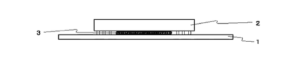
図1はボールグリッドアレイ型半導体パッケージ2と放熱器4の接着に使用したものを示す。図2はチップサイズ型半導体パッケージ2とプリント基板1の接着に使用したものを示す。図3はピングリッドアレイ型半導体パッケージ2とヒートシンク5の接着に使用したものを示す。図4は半導体チップ8とダイパッド7の接着に使用したものを示す。
【0023】
なお、熱伝導性接着剤は、スクリーン印刷、パッド印刷、ディスペンサー塗布、ポッティング、スプレー塗装などの公知の方法によって被着体間に介在させることができる。発熱する素子としては、半導体素子、電源あるいは光源など、伝熱部材としては、通常の放熱器や冷却器、ヒートシンク、ヒートスプレッダー、ダイパッド、プリント基板、冷却ファン、ヒートパイプあるいは筐体などが挙げられる。
【0024】
以下、実施例をあげて本発明をさらに詳細に説明する。なお、下記の実施例、比較例の熱伝導性は、熱抵抗値を測定することによって評価した。
【実施例1】
アミノシラン系カップリング剤で処理した六方晶系の鱗片状窒化ホウ素粉末(昭和電工株式会社製 UHP−S1 平均粒径1〜2μm)40重量部と、接着性高分子としてアミン系硬化剤を含むビスフェノールF型エポキシ樹脂100重量部を混合し、真空脱泡して熱伝導性接着剤Aを調製した。
【0025】
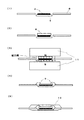
図5(1)に記すプリント基板1に実装したボールグリッドアレイ型の半導体パッケージ2上に熱伝導性接着剤Aをディスペンサーで塗布した(図5(2))。図5(3)のように熱伝導性接着剤Aの上部に放熱器1を配置して加圧し、図5(4)のように磁束密度0.6テスラの永久磁石11のN極とS極を対向させた磁場雰囲気で3の熱伝導性接着剤Aを加熱硬化させて電子部品(図5(5))を調製した。
装置に通電して6分後の熱抵抗を測定した結果、0.48℃/Wであった。
【0026】
【比較例1】
図5(1)に記すプリント基板1に実装したボールグリッドアレイ型の半導体パッケージ2上に実施例1と同様の熱伝導性接着剤Aをディスペンサーで塗布した(図5(2))。図5(3)のように熱伝導性接着剤Aの上部に放熱器4を配置して加圧し磁場を印加せずに熱伝導性接着剤Aを加熱硬化させて電子部品(図5(5))を調製した。
装置に通電して6分後の熱抵抗を測定した結果、0.61℃/Wであった。
【0027】
【実施例2】
六方晶系の鱗片状窒化ホウ素粉末(昭和電工株式会社製 UHP−S1 平均粒径1〜2μm)80重量部と、接着性高分子として付加型の液状シリコーンゴム(GE東芝シリコーン株式会社製 TSE3331)100重量部を混合し、真空脱泡して熱伝導性接着剤Bを調製した。
実施例1と同様に図5(1)に記すプリント基板1に実装したボールグリッドアレイ型の半導体パッケージ2上に熱伝導性接着剤Bをディスペンサーで塗布した(図5(2))。図5(3)のように熱伝導性接着剤Bの上部に放熱器1を配置して加圧し、図5(4)のように磁束密度2テスラの電磁石11のN極とS極を対向させた磁場雰囲気で熱伝導性接着剤Bを加熱硬化させて電子部品(図5(5))を調製した。
装置に通電して6分後の熱抵抗を測定した結果、0.37℃/Wであった。
【0028】
【比較例2】
図5(1)に記すプリント基板1に実装したボールグリッドアレイ型の半導体パッケージ2上に実施例2と同様の熱伝導性接着剤Bをディスペンサーで塗布した(図5(2))。図5(3)のように熱伝導性接着剤Bの上部に放熱器1を配置して加圧し磁場を印加せずに熱伝導性接着剤Bを加熱硬化させて電子部品(図5(5))を調製した。
装置に通電して6分後の熱抵抗を測定した結果、0.48℃/Wであった。
【0029】
【実施例3】
六方晶系の微粉状窒化ホウ素粉末(電気化学工業株式会社製 SP−1 平均粒径0.6μm)120重量部と、接着性高分子として熱硬化性ポリイミド(宇部興産株式会社製 ユピタイトUPA−83)100重量部を混合し、真空脱泡して熱伝導性接着剤Cを調製した。
【0030】
図6(1)に記すリードフレーム6のダイパッド7上に、熱伝導性接着剤Cをスクリーン印刷した(図6(1))。図6(2)のように熱伝導性接着剤Cの上部に半導体チップ8を配置して加圧し、図6(3)のように磁束密度2テスラの電磁石11のN極とS極を対向させた磁場雰囲気で熱伝導性接着剤Cを加熱硬化させた。さらにボンディングワイヤー9で半導体チップ8の電極部とリードフレーム11のリード部を電気的に接続し(図6(4))、エポキシ系封止剤10でトランスファーモールドして電子部品(図6(5))を製造した。
装置に通電して6分後の熱抵抗を測定した結果、0.28℃/Wであった。
【0031】
【比較例3】
図6(1)に記すリードフレーム6のダイパッド7上に、実施例3と同様の熱伝導性接着剤Cをスクリーン印刷した(図6(1))。図6(2)のように熱伝導性接着剤Cの上部に半導体チップ8を配置して加圧し磁場を印加せずに熱伝導性接着剤Cを加熱硬化させた。さらにボンディングワイヤー9で半導体チップ8の電極部とリードフレーム11のリード部を電気的に接続し(図6(4))、エポキシ系封止剤10でトランスファーモールドして電子部品(図6(5))を製造した。
装置に通電して6分後の熱抵抗を測定した結果、0.40℃/Wであった。
【0032】
【発明の効果】
比較例1〜比較例3に比べ、本発明の実施例1〜実施例3の接着方法で製造される電子部品は、熱伝導性接着剤中の窒化ホウ素粉末を磁場配向させることによって熱抵抗値が小さく熱伝導性にすぐれていることがわかる。従って、本発明の接着方法によれば、発熱量が大きい半導体パッケージとヒートシンクなどの放熱器との接着、あるいは発熱量が大きい半導体チップとダイパッド部との接着などに広範囲に応用することが可能になり、熱抵抗が小さく放熱特性にすぐれる有用な電子部品を提供することができる。
【図面の簡単な説明】
【図1】本発明の接着方法で作製した電子部品の例
【図2】本発明の接着方法で作製した電子部品の例
【図3】本発明の接着方法で作製した電子部品の例
【図4】本発明の接着方法で作製した電子部品の例
【図5】本発明の接着方法および電子部品を示す概略図
【図6】本発明の接着方法および電子部品を示す概略図
【符号の説明】
1 プリント基板
2 電子部品
3 熱伝導性接着剤
4 放熱器
5 ヒートシンク
6 リードフレーム
7 ダイパッド
8 半導体チップ
9 ボンディングワイヤー
10 封止剤
11 磁石
Claims (12)
- 被着体間に、窒化ホウ素粉末と接着性高分子とを配合してなる熱伝導性接着剤を介在させ、磁場雰囲気で熱伝導性接着剤中の窒化ホウ素粉末を一定方向に配向させて接着することを特徴とする接着方法。
- 前記熱伝導性接着剤が、前記接着性高分子100重量部に対して前記窒化ホウ素粉末10〜400重量部である請求項1に記載の接着方法。
- 前記接着性高分子がエポキシ系、ポリイミド系、アクリル系、ウレタン系あるいはシリコーン系より選ばれる少なくとも1種である請求項1又は請求項2に記載の接着方法。
- 前記熱伝導性接着剤の厚み方向に磁石のN極とS極を対向させて設置することで前記磁場雰囲気を発生させることを特徴とする請求項1〜請求項3の何れか1項記載の接着方法。
- 前記熱伝導性接着剤の厚み方向に対して垂直の方向に磁石のN極とS極を対向させて設置する、又は、該厚み方向に磁石のN極とN極若しくはS極とS極を対向させて設置することで、前記磁場雰囲気を発生させることを特徴とする請求項1〜請求項3の何れか1項に記載の接着方法。
- 前記被着体間が、半導体素子、電源又は光源である発熱する素子と、放熱器、冷却器、ヒートシンク、ヒートスプレッダー、ダイパッド、プリント基板、冷却ファン、ヒートパイプ又は筐体である伝熱部材との間である請求項1〜請求項5の何れか1項に記載の接着方法。
- 発熱する素子と伝熱部材間とを接着させる電子部品の製造方法であって、
該発熱する素子と該伝熱部材間に、窒化ホウ素粉末と接着性高分子とを配合してなる熱伝導性接着剤を介在させ、磁場雰囲気で熱伝導性接着剤中の窒化ホウ素粉末を一定方向に配向させた状態で接着させること特徴とする電子部品の製造方法。 - 前記熱伝導性接着剤が、前記接着性高分子100重量部に対して前記窒化ホウ素粉末10〜400重量部である請求項7に記載の電子部品の製造方法。
- 前記接着性高分子がエポキシ系、ポリイミド系、アクリル系、ウレタン系あるいはシリコーン系より選ばれる少なくとも1種である請求項7又は請求項8に記載の電子部品の製造方法。
- 前記熱伝導性接着剤の厚み方向に磁石のN極とS極を対向させて設置することで前記磁場雰囲気を発生させることを特徴とする請求項7〜請求項9の何れか1項に記載の電子部品の製造方法。
- 前記熱伝導性接着剤の厚み方向に対して垂直の方向に磁石のN極とS極を対向させて設置する、又は、該厚み方向に磁石のN極とN極若しくはS極とS極を対向させて設置することで、前記磁場雰囲気を発生させることを特徴とする請求項7〜請求項9の何れか1項に記載の電子部品の製造方法。
- 前記発熱する素子が半導体素子、電源又は光源であり、
前記伝熱部材が放熱器、冷却器、ヒートシンク、ヒートスプレッダー、ダイパッド、プリント基板、冷却ファン、ヒートパイプ又は筐体である請求項7〜請求項11の何れか1項記載の電子部品の製造方法。
Priority Applications (5)
| Application Number | Priority Date | Filing Date | Title |
|---|---|---|---|
| JP35864799A JP4528397B2 (ja) | 1999-12-17 | 1999-12-17 | 接着方法および電子部品 |
| US09/733,560 US6649012B2 (en) | 1999-12-17 | 2000-12-08 | Adhesion method and electronic component |
| EP00311186A EP1108766B1 (en) | 1999-12-17 | 2000-12-14 | Adhesion method and electronic component |
| DE60009646T DE60009646T2 (de) | 1999-12-17 | 2000-12-14 | Klebeverfahren und elektronisches Bauteil |
| US10/655,239 US6918983B2 (en) | 1999-12-17 | 2003-09-04 | Adhesion method and electronic component |
Applications Claiming Priority (1)
| Application Number | Priority Date | Filing Date | Title |
|---|---|---|---|
| JP35864799A JP4528397B2 (ja) | 1999-12-17 | 1999-12-17 | 接着方法および電子部品 |
Publications (2)
| Publication Number | Publication Date |
|---|---|
| JP2001172604A JP2001172604A (ja) | 2001-06-26 |
| JP4528397B2 true JP4528397B2 (ja) | 2010-08-18 |
Family
ID=18460401
Family Applications (1)
| Application Number | Title | Priority Date | Filing Date |
|---|---|---|---|
| JP35864799A Expired - Fee Related JP4528397B2 (ja) | 1999-12-17 | 1999-12-17 | 接着方法および電子部品 |
Country Status (4)
| Country | Link |
|---|---|
| US (2) | US6649012B2 (ja) |
| EP (1) | EP1108766B1 (ja) |
| JP (1) | JP4528397B2 (ja) |
| DE (1) | DE60009646T2 (ja) |
Families Citing this family (85)
| Publication number | Priority date | Publication date | Assignee | Title |
|---|---|---|---|---|
| JP2001172398A (ja) * | 1999-12-17 | 2001-06-26 | Polymatech Co Ltd | 熱伝導性成形体およびその製造方法 |
| JP3468420B2 (ja) * | 2000-06-07 | 2003-11-17 | 持田商工株式会社 | 放熱シート及びその製造方法 |
| WO2002084631A1 (en) * | 2001-04-11 | 2002-10-24 | Sony Corporation | Element transfer method, element arrangmenet method using the same, and image display apparatus production method |
| DE10120928C1 (de) * | 2001-04-30 | 2002-10-31 | Infineon Technologies Ag | Verfahren zum Erstellen einer Kontaktverbindung zwischen einem Halbleiterchip und einem Substrat, insbesondere zwischen einem Speichermodulchip und einem Speichermodulboard |
| US6645612B2 (en) | 2001-08-07 | 2003-11-11 | Saint-Gobain Ceramics & Plastics, Inc. | High solids hBN slurry, hBN paste, spherical hBN powder, and methods of making and using them |
| US20030095388A1 (en) * | 2001-11-16 | 2003-05-22 | Jinbao Jiao | Method and apparatus for securing a circuit board to a rigid surface |
| US7147367B2 (en) * | 2002-06-11 | 2006-12-12 | Saint-Gobain Performance Plastics Corporation | Thermal interface material with low melting alloy |
| US7210227B2 (en) * | 2002-11-26 | 2007-05-01 | Intel Corporation | Decreasing thermal contact resistance at a material interface |
| US6916688B1 (en) * | 2002-12-05 | 2005-07-12 | National Semiconductor Corporation | Apparatus and method for a wafer level chip scale package heat sink |
| US7494635B2 (en) | 2003-08-21 | 2009-02-24 | Saint-Gobain Ceramics & Plastics, Inc. | Boron nitride agglomerated powder |
| US7180173B2 (en) * | 2003-11-20 | 2007-02-20 | Taiwan Semiconductor Manufacturing Co. Ltd. | Heat spreader ball grid array (HSBGA) design for low-k integrated circuits (IC) |
| US7145179B2 (en) * | 2004-10-12 | 2006-12-05 | Gelcore Llc | Magnetic attachment method for LED light engines |
| JP4686274B2 (ja) * | 2005-06-30 | 2011-05-25 | ポリマテック株式会社 | 放熱部品及びその製造方法 |
| US7236562B2 (en) * | 2005-11-03 | 2007-06-26 | General Electric Company | Method of assembly and thermal management of CT detector electronics circuits |
| JP2007145677A (ja) * | 2005-11-30 | 2007-06-14 | Teijin Ltd | 芳香族ポリアミドにより被覆された窒化ホウ素ナノチューブ |
| JP4922018B2 (ja) | 2007-03-06 | 2012-04-25 | 株式会社東芝 | 回転電機のコイル絶縁物 |
| DE102007039902A1 (de) * | 2007-08-23 | 2008-10-16 | Siemens Ag | Wärmeleitmaterial mit zwei Materialbestandteilen und Verwendung des Wärmeleitmaterials |
| DE102007045418B4 (de) * | 2007-09-21 | 2011-05-12 | Sew-Eurodrive Gmbh & Co. Kg | Herstellungsverfahren für eine Anordnung zum Kühlen eines elektrischen Bauelements |
| CN101855680B (zh) * | 2007-09-27 | 2013-06-19 | 韦沙戴尔电子公司 | 功率电阻器 |
| US7906373B1 (en) * | 2008-03-26 | 2011-03-15 | Pawel Czubarow | Thermally enhanced electrically insulative adhesive paste |
| JP5344880B2 (ja) * | 2008-10-01 | 2013-11-20 | 三井化学株式会社 | 接着樹脂組成物、およびそれを含む積層体 |
| JP5703287B2 (ja) * | 2009-03-31 | 2015-04-15 | サノフィ−アベンティス・ドイチュラント・ゲゼルシャフト・ミット・ベシュレンクテル・ハフツング | 接着剤を使用する薬物送達デバイス本体の製造方法及び薬物送達デバイス本体 |
| US8287996B2 (en) | 2009-12-21 | 2012-10-16 | Intel Corporation | Coating for a microelectronic device, treatment comprising same, and method of managing a thermal profile of a microelectronic die |
| US8749978B2 (en) * | 2010-01-29 | 2014-06-10 | Nitto Denko Corporation | Power module |
| JP2012039064A (ja) * | 2010-01-29 | 2012-02-23 | Nitto Denko Corp | 熱伝導性シート |
| US8592844B2 (en) | 2010-01-29 | 2013-11-26 | Nitto Denko Corporation | Light-emitting diode device |
| TWI513810B (zh) | 2010-01-29 | 2015-12-21 | 日東電工股份有限公司 | 攝像零件 |
| DE102010050900A1 (de) | 2010-11-10 | 2012-05-10 | Esk Ceramics Gmbh & Co. Kg | Bornitrid-Agglomerate, Verfahren zu deren Herstellung und deren Verwendung |
| JP2012253151A (ja) * | 2011-06-01 | 2012-12-20 | Toyota Industries Corp | 電子機器 |
| JP5619830B2 (ja) * | 2011-08-24 | 2014-11-05 | パナソニック株式会社 | 樹脂−反磁性物質複合構造体、その製造方法、およびそれを用いた半導体装置 |
| DE102012201426A1 (de) * | 2012-02-01 | 2013-08-01 | Leibniz-Institut Für Polymerforschung Dresden E.V. | Verfahren zum verbinden von kunststoffen und verfahren zum lösen einer verbindung im kunststoffverbund und kunststoffverbund |
| US20150274930A1 (en) * | 2012-09-19 | 2015-10-01 | Momentive Performance Materials Inc. | Masterbatch comprising boron nitride, composite powders thereof, and compositions and articles comprising such materials |
| US20140252566A1 (en) * | 2013-03-06 | 2014-09-11 | Rf Micro Devices, Inc. | Silicon-on-dual plastic (sodp) technology and methods of manufacturing the same |
| US9214337B2 (en) | 2013-03-06 | 2015-12-15 | Rf Micro Devices, Inc. | Patterned silicon-on-plastic (SOP) technology and methods of manufacturing the same |
| US9583414B2 (en) | 2013-10-31 | 2017-02-28 | Qorvo Us, Inc. | Silicon-on-plastic semiconductor device and method of making the same |
| US9812350B2 (en) | 2013-03-06 | 2017-11-07 | Qorvo Us, Inc. | Method of manufacture for a silicon-on-plastic semiconductor device with interfacial adhesion layer |
| US9464214B2 (en) * | 2014-02-25 | 2016-10-11 | The Boeing Company | Thermally conductive flexible adhesive for aerospace applications |
| TWI582847B (zh) | 2014-09-12 | 2017-05-11 | Rf微型儀器公司 | 包含具有聚合物基板之半導體裝置的印刷電路模組及其製造方法 |
| US10085352B2 (en) | 2014-10-01 | 2018-09-25 | Qorvo Us, Inc. | Method for manufacturing an integrated circuit package |
| US10121718B2 (en) | 2014-11-03 | 2018-11-06 | Qorvo Us, Inc. | Printed circuit module having a semiconductor device with a protective layer in place of a low-resistivity handle layer |
| US9960145B2 (en) | 2015-03-25 | 2018-05-01 | Qorvo Us, Inc. | Flip chip module with enhanced properties |
| US9613831B2 (en) | 2015-03-25 | 2017-04-04 | Qorvo Us, Inc. | Encapsulated dies with enhanced thermal performance |
| US20160343604A1 (en) | 2015-05-22 | 2016-11-24 | Rf Micro Devices, Inc. | Substrate structure with embedded layer for post-processing silicon handle elimination |
| US10276495B2 (en) | 2015-09-11 | 2019-04-30 | Qorvo Us, Inc. | Backside semiconductor die trimming |
| US10020405B2 (en) | 2016-01-19 | 2018-07-10 | Qorvo Us, Inc. | Microelectronics package with integrated sensors |
| US20170227167A1 (en) * | 2016-02-05 | 2017-08-10 | Chung-Ping Lai | Light-emitting diode filament lamp |
| US10062583B2 (en) | 2016-05-09 | 2018-08-28 | Qorvo Us, Inc. | Microelectronics package with inductive element and magnetically enhanced mold compound component |
| US10773952B2 (en) | 2016-05-20 | 2020-09-15 | Qorvo Us, Inc. | Wafer-level package with enhanced performance |
| US10784149B2 (en) | 2016-05-20 | 2020-09-22 | Qorvo Us, Inc. | Air-cavity module with enhanced device isolation |
| US10103080B2 (en) | 2016-06-10 | 2018-10-16 | Qorvo Us, Inc. | Thermally enhanced semiconductor package with thermal additive and process for making the same |
| US10079196B2 (en) | 2016-07-18 | 2018-09-18 | Qorvo Us, Inc. | Thermally enhanced semiconductor package having field effect transistors with back-gate feature |
| WO2018031995A1 (en) | 2016-08-12 | 2018-02-15 | Qorvo Us, Inc. | Wafer-level package with enhanced performance |
| EP3497719B1 (en) | 2016-08-12 | 2020-06-10 | Qorvo Us, Inc. | Wafer-level package with enhanced performance |
| EP3497718B1 (en) | 2016-08-12 | 2025-11-19 | Qorvo Us, Inc. | Wafer-level package with enhanced performance and corresponding method |
| US10109502B2 (en) | 2016-09-12 | 2018-10-23 | Qorvo Us, Inc. | Semiconductor package with reduced parasitic coupling effects and process for making the same |
| US10090339B2 (en) | 2016-10-21 | 2018-10-02 | Qorvo Us, Inc. | Radio frequency (RF) switch |
| US10749518B2 (en) | 2016-11-18 | 2020-08-18 | Qorvo Us, Inc. | Stacked field-effect transistor switch |
| US10068831B2 (en) | 2016-12-09 | 2018-09-04 | Qorvo Us, Inc. | Thermally enhanced semiconductor package and process for making the same |
| US10755992B2 (en) | 2017-07-06 | 2020-08-25 | Qorvo Us, Inc. | Wafer-level packaging for enhanced performance |
| US10784233B2 (en) | 2017-09-05 | 2020-09-22 | Qorvo Us, Inc. | Microelectronics package with self-aligned stacked-die assembly |
| US10366972B2 (en) | 2017-09-05 | 2019-07-30 | Qorvo Us, Inc. | Microelectronics package with self-aligned stacked-die assembly |
| US10283683B1 (en) * | 2018-01-18 | 2019-05-07 | Bgt Materials Limited | Filament structure and LED light bulb having the same |
| US10281129B1 (en) * | 2018-01-18 | 2019-05-07 | Bgt Materials Limited | Filament structure of LED light bulb |
| US11152363B2 (en) | 2018-03-28 | 2021-10-19 | Qorvo Us, Inc. | Bulk CMOS devices with enhanced performance and methods of forming the same utilizing bulk CMOS process |
| US12062700B2 (en) | 2018-04-04 | 2024-08-13 | Qorvo Us, Inc. | Gallium-nitride-based module with enhanced electrical performance and process for making the same |
| US12046505B2 (en) | 2018-04-20 | 2024-07-23 | Qorvo Us, Inc. | RF devices with enhanced performance and methods of forming the same utilizing localized SOI formation |
| US10804246B2 (en) | 2018-06-11 | 2020-10-13 | Qorvo Us, Inc. | Microelectronics package with vertically stacked dies |
| CN118213279A (zh) | 2018-07-02 | 2024-06-18 | Qorvo美国公司 | Rf半导体装置及其制造方法 |
| US11069590B2 (en) | 2018-10-10 | 2021-07-20 | Qorvo Us, Inc. | Wafer-level fan-out package with enhanced performance |
| US10964554B2 (en) | 2018-10-10 | 2021-03-30 | Qorvo Us, Inc. | Wafer-level fan-out package with enhanced performance |
| US11646242B2 (en) | 2018-11-29 | 2023-05-09 | Qorvo Us, Inc. | Thermally enhanced semiconductor package with at least one heat extractor and process for making the same |
| US11387157B2 (en) | 2019-01-23 | 2022-07-12 | Qorvo Us, Inc. | RF devices with enhanced performance and methods of forming the same |
| KR20250027591A (ko) | 2019-01-23 | 2025-02-26 | 코르보 유에스, 인크. | Rf 반도체 디바이스 및 이를 형성하는 방법 |
| US12057374B2 (en) | 2019-01-23 | 2024-08-06 | Qorvo Us, Inc. | RF devices with enhanced performance and methods of forming the same |
| US12125825B2 (en) | 2019-01-23 | 2024-10-22 | Qorvo Us, Inc. | RF devices with enhanced performance and methods of forming the same |
| US12046570B2 (en) | 2019-01-23 | 2024-07-23 | Qorvo Us, Inc. | RF devices with enhanced performance and methods of forming the same |
| US12046483B2 (en) | 2019-01-23 | 2024-07-23 | Qorvo Us, Inc. | RF devices with enhanced performance and methods of forming the same |
| US12074086B2 (en) | 2019-11-01 | 2024-08-27 | Qorvo Us, Inc. | RF devices with nanotube particles for enhanced performance and methods of forming the same |
| US11646289B2 (en) | 2019-12-02 | 2023-05-09 | Qorvo Us, Inc. | RF devices with enhanced performance and methods of forming the same |
| US11923238B2 (en) | 2019-12-12 | 2024-03-05 | Qorvo Us, Inc. | Method of forming RF devices with enhanced performance including attaching a wafer to a support carrier by a bonding technique without any polymer adhesive |
| EP3835332A1 (en) * | 2019-12-13 | 2021-06-16 | Henkel AG & Co. KGaA | Thermally conductive polyurethane adhesive composition |
| US12129168B2 (en) | 2019-12-23 | 2024-10-29 | Qorvo Us, Inc. | Microelectronics package with vertically stacked MEMS device and controller device |
| US12103787B2 (en) * | 2020-02-18 | 2024-10-01 | Ev Group E. Thallner Gmbh | Method and device for transferring components |
| WO2022126016A2 (en) | 2020-12-11 | 2022-06-16 | Qorvo Us, Inc. | Multi-level 3d stacked package and methods of forming the same |
| US12062571B2 (en) | 2021-03-05 | 2024-08-13 | Qorvo Us, Inc. | Selective etching process for SiGe and doped epitaxial silicon |
Family Cites Families (12)
| Publication number | Priority date | Publication date | Assignee | Title |
|---|---|---|---|---|
| ZA741474B (en) * | 1974-03-07 | 1975-10-29 | Edenvale Eng Works | Abrasive tools |
| JPS62194653A (ja) | 1986-02-21 | 1987-08-27 | Hitachi Ltd | 半導体装置 |
| JPS6362762A (ja) | 1986-09-03 | 1988-03-19 | Hitachi Maxell Ltd | 感熱転写記録材 |
| JPH0638460B2 (ja) * | 1989-11-08 | 1994-05-18 | 東海ゴム工業株式会社 | 放熱シート |
| JPH04130175A (ja) * | 1990-09-19 | 1992-05-01 | Toray Ind Inc | エポキシ樹脂系接着剤組成物 |
| JP2915665B2 (ja) * | 1991-12-20 | 1999-07-05 | 松下電工株式会社 | 絶縁シートとそれを使った金属配線板との製造方法。 |
| CH685942A5 (fr) * | 1992-08-24 | 1995-11-15 | Battelle Memorial Institute | Procede de collage de deux substrats non metalliques a l'aide d'un adhesif. |
| JPH08245833A (ja) | 1995-01-13 | 1996-09-24 | Sumitomo Bakelite Co Ltd | 熱硬化性樹脂組成物 |
| JP3511118B2 (ja) * | 1996-08-16 | 2004-03-29 | 日立化成工業株式会社 | 接着剤、半導体装置の製造方法、および半導体装置 |
| JPH10292157A (ja) * | 1997-04-17 | 1998-11-04 | Nitto Denko Corp | 熱伝導性感圧接着シ―ト類およびこれを用いた電子部品と放熱部材との固定方法 |
| JP3434678B2 (ja) * | 1997-09-12 | 2003-08-11 | 電気化学工業株式会社 | ゴムシートの製造方法 |
| DE19841133A1 (de) | 1998-09-09 | 2000-03-16 | Abb Daimler Benz Transp | Modul einer, vorzugsweise in einem Antrieb für ein Schienenfahrzeug enthaltenen, modular aufgebauten Schaltungsanordnung |
-
1999
- 1999-12-17 JP JP35864799A patent/JP4528397B2/ja not_active Expired - Fee Related
-
2000
- 2000-12-08 US US09/733,560 patent/US6649012B2/en not_active Expired - Fee Related
- 2000-12-14 EP EP00311186A patent/EP1108766B1/en not_active Expired - Lifetime
- 2000-12-14 DE DE60009646T patent/DE60009646T2/de not_active Expired - Lifetime
-
2003
- 2003-09-04 US US10/655,239 patent/US6918983B2/en not_active Expired - Fee Related
Also Published As
| Publication number | Publication date |
|---|---|
| EP1108766A9 (en) | 2002-04-03 |
| JP2001172604A (ja) | 2001-06-26 |
| US20040041257A1 (en) | 2004-03-04 |
| US20010004131A1 (en) | 2001-06-21 |
| US6649012B2 (en) | 2003-11-18 |
| US6918983B2 (en) | 2005-07-19 |
| EP1108766A3 (en) | 2001-09-19 |
| EP1108766A2 (en) | 2001-06-20 |
| DE60009646T2 (de) | 2005-03-31 |
| DE60009646D1 (de) | 2004-05-13 |
| EP1108766B1 (en) | 2004-04-07 |
Similar Documents
| Publication | Publication Date | Title |
|---|---|---|
| JP4528397B2 (ja) | 接着方法および電子部品 | |
| US6663969B2 (en) | Heat conductive adhesive film and manufacturing method thereof and electronic component | |
| US6660566B2 (en) | Heat conductive molded body and manufacturing method thereof and semiconductor device | |
| JP7053579B2 (ja) | 伝熱部材及びこれを含む放熱構造体 | |
| JP5184543B2 (ja) | 熱伝導性シート及びパワーモジュール | |
| JP2000281995A (ja) | 熱伝導性接着フィルムおよび半導体装置 | |
| US7041535B2 (en) | Power module and method of manufacturing the same | |
| EP1109218B1 (en) | Heat conducting mold and manufacturing method thereof | |
| JP4089636B2 (ja) | 熱伝導性樹脂シートの製造方法およびパワーモジュールの製造方法 | |
| JP2000195998A (ja) | 熱伝導性シ―トおよびその製造方法ならびに半導体装置 | |
| CN1893803A (zh) | 散热部件及其制造方法 | |
| JP2000191987A (ja) | 熱伝導性接着フィルムおよび半導体装置 | |
| JP6518902B2 (ja) | 熱伝導性部材、熱伝導性組成物および熱伝導性組成物の製造方法 | |
| JP2011178894A (ja) | 熱硬化性樹脂組成物、熱伝導性シート及びパワーモジュール | |
| JP2002146672A (ja) | 熱伝導性充填剤及び熱伝導性接着剤並びに半導体装置 | |
| JP2008153430A (ja) | 放熱基板並びに熱伝導性シートおよびこれらを用いたパワーモジュール | |
| JP5274007B2 (ja) | 熱伝導性樹脂シートおよびこれを用いたパワーモジュール | |
| JP2000273426A (ja) | 熱伝導性接着剤および接着方法ならびに半導体装置 | |
| JP2001081418A (ja) | 熱伝導性接着フィルムおよびその製造方法ならびに電子部品 | |
| JP2000191998A (ja) | 熱伝導性接着剤および接着方法ならびに半導体装置 | |
| JP4272767B2 (ja) | 熱伝導性成形体およびその製造方法ならびに導体回路用樹脂基板およびその製造方法 | |
| JP4709339B2 (ja) | 熱伝導性接着剤および接着方法ならびに電子部品 | |
| JP2002003717A (ja) | 熱伝導性シート | |
| JP2000022289A (ja) | 回路基板用樹脂組成物とそれを用いた回路基板 | |
| JP2003192913A (ja) | 熱伝導性樹脂組成物およびそれを使用した電子部品装置 |
Legal Events
| Date | Code | Title | Description |
|---|---|---|---|
| A621 | Written request for application examination |
Free format text: JAPANESE INTERMEDIATE CODE: A621 Effective date: 20061122 |
|
| A977 | Report on retrieval |
Free format text: JAPANESE INTERMEDIATE CODE: A971007 Effective date: 20100208 |
|
| A131 | Notification of reasons for refusal |
Free format text: JAPANESE INTERMEDIATE CODE: A131 Effective date: 20100215 |
|
| A521 | Request for written amendment filed |
Free format text: JAPANESE INTERMEDIATE CODE: A523 Effective date: 20100409 |
|
| TRDD | Decision of grant or rejection written | ||
| A01 | Written decision to grant a patent or to grant a registration (utility model) |
Free format text: JAPANESE INTERMEDIATE CODE: A01 Effective date: 20100511 |
|
| A01 | Written decision to grant a patent or to grant a registration (utility model) |
Free format text: JAPANESE INTERMEDIATE CODE: A01 |
|
| A61 | First payment of annual fees (during grant procedure) |
Free format text: JAPANESE INTERMEDIATE CODE: A61 Effective date: 20100607 |
|
| FPAY | Renewal fee payment (event date is renewal date of database) |
Free format text: PAYMENT UNTIL: 20130611 Year of fee payment: 3 |
|
| R150 | Certificate of patent or registration of utility model |
Free format text: JAPANESE INTERMEDIATE CODE: R150 |
|
| LAPS | Cancellation because of no payment of annual fees |