JP4513402B2 - チップ型ptcサーミスタ素子 - Google Patents
チップ型ptcサーミスタ素子 Download PDFInfo
- Publication number
- JP4513402B2 JP4513402B2 JP2004134136A JP2004134136A JP4513402B2 JP 4513402 B2 JP4513402 B2 JP 4513402B2 JP 2004134136 A JP2004134136 A JP 2004134136A JP 2004134136 A JP2004134136 A JP 2004134136A JP 4513402 B2 JP4513402 B2 JP 4513402B2
- Authority
- JP
- Japan
- Prior art keywords
- ptc thermistor
- thermistor element
- type ptc
- value
- chip
- Prior art date
- Legal status (The legal status is an assumption and is not a legal conclusion. Google has not performed a legal analysis and makes no representation as to the accuracy of the status listed.)
- Expired - Lifetime
Links
Images

Landscapes
- Compositions Of Oxide Ceramics (AREA)
- Thermistors And Varistors (AREA)
Description
例えば、特許文献1に記載されているように、Pbを含むチタン酸バリウム系の材料組成からなる単板型PTCサーミスタ素子が開示されている。ここで、その組成式をABxO3と表した時、そのPTCサーミスタ素子のセラミック焼結体内部は、x=1.000(x値はAサイト成分とBサイト成分のモル比、すなわちB/A値を示す)となっていることが一般的である。
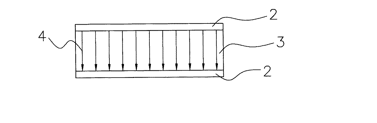
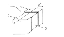
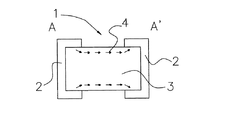
2 端子電極
3 セラミック焼結体
4 電流の流れ
Claims (1)
- Baの一部をPbで置換したチタン酸バリウムを主成分としたセラミック焼結体の両端であって、前記セラミック焼結体のそれぞれ5面にまたがる端子電極を形成させた、チップ型PTCサーミスタ素子であって、前記主成分の組成式をABxO3で表した場合、xが0.992以上0.999以下であることを特徴とする、チップ型PTCサーミスタ素子。
Priority Applications (1)
| Application Number | Priority Date | Filing Date | Title |
|---|---|---|---|
| JP2004134136A JP4513402B2 (ja) | 2004-04-28 | 2004-04-28 | チップ型ptcサーミスタ素子 |
Applications Claiming Priority (1)
| Application Number | Priority Date | Filing Date | Title |
|---|---|---|---|
| JP2004134136A JP4513402B2 (ja) | 2004-04-28 | 2004-04-28 | チップ型ptcサーミスタ素子 |
Publications (2)
| Publication Number | Publication Date |
|---|---|
| JP2005317780A JP2005317780A (ja) | 2005-11-10 |
| JP4513402B2 true JP4513402B2 (ja) | 2010-07-28 |
Family
ID=35444879
Family Applications (1)
| Application Number | Title | Priority Date | Filing Date |
|---|---|---|---|
| JP2004134136A Expired - Lifetime JP4513402B2 (ja) | 2004-04-28 | 2004-04-28 | チップ型ptcサーミスタ素子 |
Country Status (1)
| Country | Link |
|---|---|
| JP (1) | JP4513402B2 (ja) |
Family Cites Families (5)
| Publication number | Priority date | Publication date | Assignee | Title |
|---|---|---|---|---|
| JPS6328324A (ja) * | 1986-07-23 | 1988-02-06 | 八尋産業株式会社 | 椎茸の人工ほだ木栽培方法と、この方法に用いる人工ほだ木成型容器 |
| JPH05326204A (ja) * | 1992-05-25 | 1993-12-10 | Murata Mfg Co Ltd | チップ型ptcサーミスタ |
| JP3286855B2 (ja) * | 1992-11-09 | 2002-05-27 | 株式会社村田製作所 | チップ型ptcサーミスタの製造方法 |
| US5658485A (en) * | 1995-10-03 | 1997-08-19 | Lucent Technologies Inc. | Pyrochlore based oxides with high dielectric constant and low temperature coefficient |
| JP3555395B2 (ja) * | 1997-06-25 | 2004-08-18 | 宇部興産株式会社 | チタン酸バリウム鉛系半導体磁器組成物 |
-
2004
- 2004-04-28 JP JP2004134136A patent/JP4513402B2/ja not_active Expired - Lifetime
Also Published As
| Publication number | Publication date |
|---|---|
| JP2005317780A (ja) | 2005-11-10 |
Similar Documents
| Publication | Publication Date | Title |
|---|---|---|
| JP5413458B2 (ja) | チタン酸バリウム系半導体磁器組成物およびチタン酸バリウム系半導体磁器素子 | |
| KR100320723B1 (ko) | 티탄산바륨계 반도체 세라믹 조성물 | |
| KR101099356B1 (ko) | 칩형 반도체 세라믹 전자부품 | |
| KR20170016805A (ko) | 반도체 자기 조성물 및 ptc 서미스터 | |
| JP5223927B2 (ja) | チタン酸バリウム系半導体磁器組成物及びptcサーミスタ | |
| JP2008174413A (ja) | 誘電体磁器組成物および電子部品 | |
| JP5418323B2 (ja) | 誘電体磁器組成物および電子部品 | |
| JP5817839B2 (ja) | Ptcサーミスタおよびptcサーミスタの製造方法 | |
| JP2016054225A (ja) | 負特性サーミスタ用半導体セラミック組成物および負特性サーミスタ | |
| JP6447841B2 (ja) | チタン酸バリウム系半導体セラミック、チタン酸バリウム系半導体セラミック組成物および温度検知用正特性サーミスタ | |
| JP4513402B2 (ja) | チップ型ptcサーミスタ素子 | |
| JPH06151103A (ja) | 積層型半導体磁器組成物 | |
| JP4548431B2 (ja) | サーミスタ組成物及びサーミスタ素子 | |
| JP5881169B2 (ja) | 半導体磁器組成物の製造方法 | |
| JP2014072374A (ja) | チタン酸バリウム系半導体磁器組成物およびそれを用いたptcサーミスタ | |
| JP5988388B2 (ja) | 半導体磁器組成物およびその製造方法 | |
| JP5668569B2 (ja) | 誘電体磁器組成物および電子部品 | |
| JP6020068B2 (ja) | 誘電体磁器組成物および電子部品 | |
| JP4710574B2 (ja) | 誘電体磁器組成物および電子部品 | |
| JP2016184694A (ja) | 半導体磁器組成物およびptcサーミスタ | |
| JP2002193665A (ja) | サーミスタ用半導体磁器及びそれを用いたチップ型サーミスタ | |
| JP6075877B2 (ja) | 半導体磁器組成物およびその製造方法 | |
| JP4779466B2 (ja) | チタン酸バリウム系半導体磁器組成物 | |
| JP2521862B2 (ja) | 誘電体磁器組成物 | |
| JP4655053B2 (ja) | サーミスタ素子 |
Legal Events
| Date | Code | Title | Description |
|---|---|---|---|
| A621 | Written request for application examination |
Free format text: JAPANESE INTERMEDIATE CODE: A621 Effective date: 20070131 |
|
| A977 | Report on retrieval |
Free format text: JAPANESE INTERMEDIATE CODE: A971007 Effective date: 20090703 |
|
| A131 | Notification of reasons for refusal |
Free format text: JAPANESE INTERMEDIATE CODE: A131 Effective date: 20090728 |
|
| A521 | Request for written amendment filed |
Free format text: JAPANESE INTERMEDIATE CODE: A523 Effective date: 20090928 |
|
| TRDD | Decision of grant or rejection written | ||
| A01 | Written decision to grant a patent or to grant a registration (utility model) |
Free format text: JAPANESE INTERMEDIATE CODE: A01 Effective date: 20100420 |
|
| A01 | Written decision to grant a patent or to grant a registration (utility model) |
Free format text: JAPANESE INTERMEDIATE CODE: A01 |
|
| A61 | First payment of annual fees (during grant procedure) |
Free format text: JAPANESE INTERMEDIATE CODE: A61 Effective date: 20100503 |
|
| R150 | Certificate of patent or registration of utility model |
Ref document number: 4513402 Country of ref document: JP Free format text: JAPANESE INTERMEDIATE CODE: R150 Free format text: JAPANESE INTERMEDIATE CODE: R150 |
|
| FPAY | Renewal fee payment (event date is renewal date of database) |
Free format text: PAYMENT UNTIL: 20130521 Year of fee payment: 3 |
|
| FPAY | Renewal fee payment (event date is renewal date of database) |
Free format text: PAYMENT UNTIL: 20130521 Year of fee payment: 3 |
|
| FPAY | Renewal fee payment (event date is renewal date of database) |
Free format text: PAYMENT UNTIL: 20140521 Year of fee payment: 4 |
|
| EXPY | Cancellation because of completion of term |