JP4513402B2 - Chip type PTC thermistor element - Google Patents
Chip type PTC thermistor element Download PDFInfo
- Publication number
- JP4513402B2 JP4513402B2 JP2004134136A JP2004134136A JP4513402B2 JP 4513402 B2 JP4513402 B2 JP 4513402B2 JP 2004134136 A JP2004134136 A JP 2004134136A JP 2004134136 A JP2004134136 A JP 2004134136A JP 4513402 B2 JP4513402 B2 JP 4513402B2
- Authority
- JP
- Japan
- Prior art keywords
- ptc thermistor
- thermistor element
- type ptc
- value
- chip
- Prior art date
- Legal status (The legal status is an assumption and is not a legal conclusion. Google has not performed a legal analysis and makes no representation as to the accuracy of the status listed.)
- Expired - Lifetime
Links
Images

Landscapes
- Compositions Of Oxide Ceramics (AREA)
- Thermistors And Varistors (AREA)
Description
本発明は、チップ型PTCサーミスタ素子に関するもので、特に面実装型のチップ部品として好適に用いることのできるチップ型PTCサーミスタ素子である。 The present invention relates to a chip-type PTC thermistor element, and is particularly a chip-type PTC thermistor element that can be suitably used as a surface-mount type chip component.
従来から用いられている単板型PTCサーミスタ素子は、半導体磁器組成物からなるセラミック焼結体の両主面に導電ペーストを塗布し、これを焼き付けて端子電極を形成することによって、製造されている。通常、上記セラミック焼結体は、仮焼粉を円板状に圧縮成形し、所望の焼成条件で焼成して得られる。
例えば、特許文献1に記載されているように、Pbを含むチタン酸バリウム系の材料組成からなる単板型PTCサーミスタ素子が開示されている。ここで、その組成式をABxO3と表した時、そのPTCサーミスタ素子のセラミック焼結体内部は、x=1.000(x値はAサイト成分とBサイト成分のモル比、すなわちB/A値を示す)となっていることが一般的である。
For example, as described in
現在における電子部品の小型化・高密度化に伴い、面実装型のチップ部品が非常に強く求められている。 With the downsizing and increasing density of electronic components at present, surface-mounted chip components are strongly demanded.
しかしながら、上記特許文献1に記載されているように、従来の単板型PTCサーミスタ素子を構成するPbを含むチタン酸バリウム系の主成分の材料組成、より具体的には、主成分の組成式をABxO3と表した時にx=1.000である材料組成を、チップ型PTCサーミスタ素子に適用すると、抵抗値ばらつきが大きくなったり、抵抗温度特性の立ち上がりが悪くなったりするという問題点が顕在化する。
However, as described in
この原因については、以下のように考えられる。すなわち、後で述べるように、チップ型PTCサーミスタ素子では、その両端にある端子電極は5面電極構造となっており、上記端子電極間に電圧を印加させた場合、上記素子のセラミック焼結体における表面近傍を電流が流れる。また、上記素子を構成するセラミックを焼成する際に、上記セラミックに含有するPb成分が飛散しやすいことがよく知られている。さらに、Pb成分の飛散は、上記セラミック焼結体の部位により異なっており、上記素子のセラミック焼結体の内部よりも表面の方がPb成分の飛散量は顕著である。一方では、Baの一部をPbで置換したチタン酸バリウム系のセラミック焼結体は、その主成分の組成式をABxO3と表した時のx値が1.0を超えると、x値が1.0以下の場合と比べて、室温での抵抗値が大きくなることが知られている。以上のことから、焼成時におけるPb成分の飛散によって、上記素子のセラミック焼結体の表面近傍におけるPb成分の飛散度合いが異なるために、室温での抵抗値が大きくなった部分を主に電流が流れることが考えられる。したがって、抵抗温度温度特性の立ち上がりが悪くなったり、抵抗値ばらつきが大きくなったりすると考えられる。 About this cause, it thinks as follows. That is, as will be described later, in the chip type PTC thermistor element, the terminal electrodes at both ends thereof have a five-face electrode structure, and when a voltage is applied between the terminal electrodes, the ceramic sintered body of the element Current flows near the surface at. Further, it is well known that the Pb component contained in the ceramic is likely to be scattered when firing the ceramic constituting the element. Further, the scattering of the Pb component differs depending on the portion of the ceramic sintered body, and the amount of the Pb component scattered is more remarkable on the surface than in the ceramic sintered body of the element. On the other hand, a barium titanate-based ceramic sintered body in which a part of Ba is substituted with Pb has an x value exceeding 1.0 when the composition formula of the main component is expressed as AB x O 3. It is known that the resistance value at room temperature is larger than when the value is 1.0 or less. From the above, since the degree of scattering of the Pb component in the vicinity of the surface of the ceramic sintered body of the element is different due to the scattering of the Pb component during firing, the current mainly flows through the portion where the resistance value at room temperature is large. It is thought that it flows. Therefore, it is considered that the rise of the resistance temperature-temperature characteristic is deteriorated and the resistance value variation is increased.
一方、従来の単板型PTCサーミスタ素子は、端子電極間に電圧を印加させた場合、上記素子のセラミック焼結体の内部を電流が流れるため、表面層の変化の影響をほとんど受けない。そのため、上記チップ型PTCサーミスタ素子に見られるような抵抗ばらつきは顕在化せず、抵抗温度特性の差も現れにくくなる。 On the other hand, the conventional single plate type PTC thermistor element is hardly affected by the change of the surface layer because a current flows inside the ceramic sintered body of the element when a voltage is applied between the terminal electrodes. For this reason, the resistance variation as seen in the chip-type PTC thermistor element does not become obvious, and the difference in resistance temperature characteristics hardly appears.
本発明の目的は、上記問題点を鑑みてなされたものであって、抵抗値ばらつきや抵抗温度特性の立ち上がりの良好な特性を有するチップ型PTCサーミスタ素子を提供することである。 An object of the present invention is to provide a chip-type PTC thermistor element that has been made in view of the above-described problems and has good resistance value variation and resistance temperature characteristic rising characteristics.
本発明に係るチップ型PTCサーミスタ素子は、Baの一部をPbで置換したチタン酸バリウムを主成分としたセラミック焼結体の表面に両端であって、前記セラミック焼結体のそれぞれ5面にまたがる端子電極を形成させた、チップ型PTCサーミスタ素子であって、前記主成分の組成式をABxO3で表した場合、x値が0.992以上0.999以下であることを特徴としている。
The chip-type PTC thermistor element according to the present invention has both ends on the surface of a ceramic sintered body mainly composed of barium titanate in which a part of Ba is substituted with Pb, and is formed on each of the 5 surfaces of the ceramic sintered body. A chip-type PTC thermistor element in which a terminal electrode is formed, wherein the x value is 0.992 or more and 0.999 or less when the composition formula of the main component is expressed by AB x O 3. Yes.
本発明に係るチップ型PTCサーミスタは、抵抗値ばらつきが20%未満と小さく、かつ、抵抗温度特性(特にα10-100)が急峻となるという特有の効果を奏する。 The chip-type PTC thermistor according to the present invention has a specific effect that the resistance value variation is as small as less than 20% and the resistance temperature characteristic (especially α 10-100 ) becomes steep.
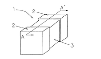
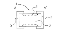
以下、この発明の実施例を図に基づいて説明する。図1は、この発明の一実施例に係るチップ型PTCサーミスタ素子の斜視図、図2はその断面図である。なお、図2には、実際には目視できないが、端子電極間に電圧を印加させた場合に発生する電流の流れについて、矢印を用いて模式的に示している。また、図3は、従来の単板型PTCサーミスタ素子の断面図である。なお、図3にも、図2と同様に、実際には目視できないが、端子電極間に電圧を印加させた場合に発生する電流の流れについて、矢印を用いて模式的に示している。 Embodiments of the present invention will be described below with reference to the drawings. FIG. 1 is a perspective view of a chip type PTC thermistor element according to one embodiment of the present invention, and FIG. 2 is a sectional view thereof. In FIG. 2, although not actually visible, the flow of current generated when a voltage is applied between the terminal electrodes is schematically shown using arrows. FIG. 3 is a cross-sectional view of a conventional single plate type PTC thermistor element. In FIG. 3, as in FIG. 2, the current flow that occurs when a voltage is applied between the terminal electrodes, although not actually visible, is schematically shown using arrows.
この実施例のチップ型PTCサーミスタ素子の製造方法は、以下に示すとおりである。 The manufacturing method of the chip type PTC thermistor element of this example is as follows.
まず、出発原料として、BaCO3,TiO2,Pb3O4,SrCO3,CaCO3,MnCO3,Er2O3,SiO2を用意した。そして、1モルの(Ba0.625Pb0.025Sr0.220Ca0.125Er0.004)TixO3に対して、MnO2換算で0.0005モル,SiO2換算で0.02モルが含有するように、上記の出発原料を所定量調合して混合した。表1には調合したxの値を示す。 First, BaCO 3 , TiO 2 , Pb 3 O 4 , SrCO 3 , CaCO 3 , MnCO 3 , Er 2 O 3 and SiO 2 were prepared as starting materials. In addition, the above-mentioned amount is 0.0005 mol in terms of MnO 2 and 0.02 mol in terms of SiO 2 with respect to 1 mol of (Ba 0.625 Pb 0.025 Sr 0.220 Ca 0.125 Er 0.004 ) Ti x O 3 . A predetermined amount of the starting material was prepared and mixed. Table 1 shows the values of x prepared.
次に、上記で得られた混合粉に、PSZ玉石および水を加えて、ボールミルを用いて、比表面積が約4m2/gとなるように混合粉砕し、その後、上記で得られた混合粉砕粉を、焼成温度が1200℃の条件で仮焼して、仮焼粉を得た。 Next, PSZ boulders and water are added to the mixed powder obtained above, and mixed and ground using a ball mill so that the specific surface area becomes about 4 m 2 / g, and then mixed and ground obtained above. The powder was calcined at a firing temperature of 1200 ° C. to obtain a calcined powder.
次に、上記で得られた仮焼粉に、バインダー等を加えて、ボールミルを用いて混合粉砕し、造粒して造粒粉を得た。 Next, a binder or the like was added to the calcined powder obtained above, mixed and ground using a ball mill, and granulated to obtain a granulated powder.
次いで、上記で得られた造粒粉を乾式プレス成形し、1.92×0.96×0.96mmのチップ形状のグリーン成形体を得た。その後、上記グリーン成形体を、焼成温度1200℃〜1350℃で2時間焼成し、1.60×0.80×0.80mmのセラミック焼結体を得た。そして、上記で得られたセラミック焼結体に端子電極を形成して、所望のチップ型PTCサーミスタを得た。なお、上記端子電極は、Cr/NiCu/Ag系の電極を用いた。チップ型PTCサーミスタの特性について、室温での抵抗値(平均値と3CV値)および抵抗温度特性(α10-100)の結果を表1に示す。 Next, the granulated powder obtained above was dry press molded to obtain a chip-shaped green molded body of 1.92 × 0.96 × 0.96 mm. Thereafter, the green molded body was fired at a firing temperature of 1200 ° C. to 1350 ° C. for 2 hours to obtain a ceramic sintered body of 1.60 × 0.80 × 0.80 mm. And the terminal electrode was formed in the ceramic sintered compact obtained above, and the desired chip type PTC thermistor was obtained. Note that a Cr / NiCu / Ag-based electrode was used as the terminal electrode. Regarding the characteristics of the chip type PTC thermistor, Table 1 shows the results of resistance values (average value and 3 CV value) at room temperature and resistance temperature characteristics (α 10-100 ).
抵抗値は、サンプル数がn=30の平均値であり、3CV値は、標準偏差σを上記平均値で除したものに3を乗じた値である。抵抗値のばらつきを示す3CV値は、実用的に使用するためには20%以下であることが必要不可欠であり、したがって、20%以下を本発明の範囲内とする。 The resistance value is an average value when the number of samples is n = 30, and the 3CV value is a value obtained by dividing the standard deviation σ by the average value and multiplying by 3. The 3CV value indicating the variation in resistance value is indispensable to be 20% or less for practical use, and therefore 20% or less is within the scope of the present invention.
また、抵抗温度特性(α10-100)は、周囲温度の変化によって抵抗値がどの程度変化するのかを示す指標であり、周囲温度が10℃から100℃に変わった時の抵抗変化率(単位は%/℃)である。ここで、PTCサーミスタ素子の場合、抵抗温度特性(α10-100)の値が大きいほど、その抵抗変化を示す立ち上がりが急峻となるので、特性は良好であると判断する。 The resistance temperature characteristic (α 10-100 ) is an index showing how much the resistance value changes due to a change in ambient temperature, and the rate of change in resistance when the ambient temperature changes from 10 ° C. to 100 ° C. (unit: Is% / ° C.). Here, in the case of the PTC thermistor element, the larger the value of the resistance temperature characteristic (α 10-100 ), the steeper the rise indicating the resistance change, and thus the characteristic is judged to be better.
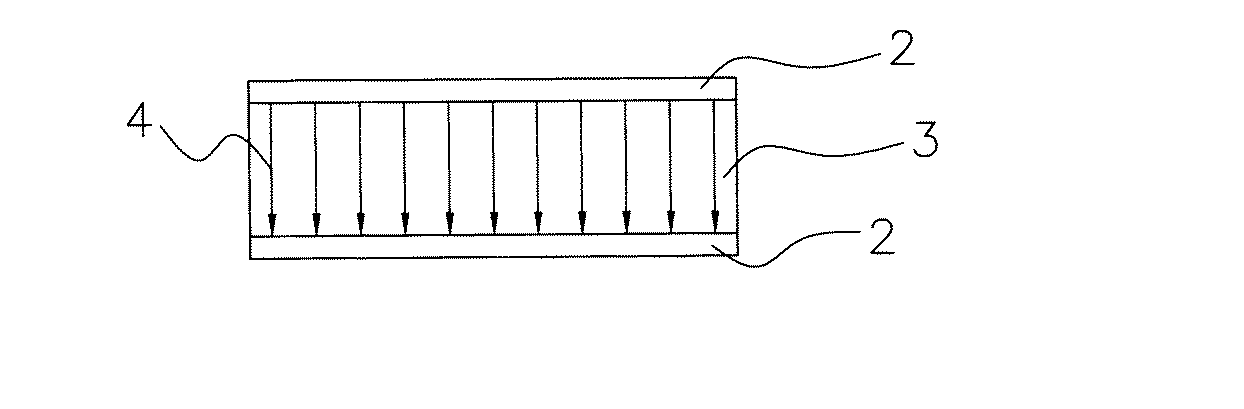
表1の結果から明らかなように、本発明の範囲内である場合、すなわち、チップ型PTCサーミスタ素子の主成分の組成式ABxO3において、x値が0.992以上0.999以下である場合、抵抗値ばらつきや抵抗温度特性の立ち上がりの良好な特性が得られる。しかしながら、x値が0.990の場合では、焼結性が悪くなるため、抵抗値ばらつきが大きくなり、また抵抗値が上昇するので、抵抗値温度特性も悪くなる。また、x値が1.000の場合では、Pb成分の飛散の影響で、抵抗値ばらつきが大きくなり、また抵抗値が上昇するので、抵抗値温度特性も悪くなる。 As is apparent from the results in Table 1, when x is 0.992 or more and 0.999 or less in the range of the present invention, that is, in the composition formula AB x O 3 of the main component of the chip type PTC thermistor element. In some cases, it is possible to obtain favorable characteristics such as resistance value variations and resistance temperature characteristics rising. However, when the x value is 0.990, the sinterability deteriorates, so that the resistance value variation becomes large, and the resistance value rises, so that the resistance temperature characteristic is also deteriorated. Also, when the x value is 1.000, the resistance value variation becomes large due to the influence of the scattering of the Pb component, and the resistance value rises, so that the resistance value temperature characteristic is also deteriorated.
ここで、チップ型PTCサーミスタ素子と単板型PTCサーミスタ素子について、Pb成分の飛散に及ぼす影響について述べる。 Here, effects of the chip type PTC thermistor element and the single plate type PTC thermistor element on the scattering of the Pb component will be described.
図1に示すように、チップ型PTCサーミスタ素子の両端にある端子電極は、それぞれ5面に電極が形成されており、端子電極間に電圧を印加させた場合に、図2に示すように、セラミック焼結体の表面近傍を電流が流れるようになる。ここで、Pb成分が飛散すると、上記x値が大きい部位を主に電流が流れるので、抵抗が上昇するようになる。また、Pb成分の飛散度合いは、上記素子のセラミック焼結体の部位により異なるので、抵抗値ばらつき(3CV値)は大きくなる。特に、従来のx値が1.000である場合では、上記の現象が顕在化する。そこで、上記問題点を解決するために、本発明では、x値が0.992〜0.999となるセラミック焼結体を用いると、Pb成分の飛散によるx値のばらつきが抵抗値に及ぼす影響は少なくなるので、抵抗値ばらつき(3CV値)を抑えることができ、それによって、抵抗温度特性の立ち上がりも向上でき、特性の安定化を図ることができると考えられる。 As shown in FIG. 1, the terminal electrodes at both ends of the chip-type PTC thermistor element have electrodes formed on five surfaces, respectively, and when a voltage is applied between the terminal electrodes, as shown in FIG. Current flows near the surface of the ceramic sintered body. Here, when the Pb component is scattered, the current mainly flows through the portion where the x value is large, so that the resistance increases. Further, since the degree of scattering of the Pb component varies depending on the portion of the ceramic sintered body of the element, the resistance value variation (3 CV value) becomes large. In particular, when the conventional x value is 1.000, the above phenomenon becomes obvious. Therefore, in order to solve the above problems, in the present invention, when a ceramic sintered body having an x value of 0.992 to 0.999 is used, the influence of variation in the x value due to scattering of the Pb component on the resistance value. Therefore, it is considered that the variation in resistance value (3CV value) can be suppressed, whereby the rise of the resistance temperature characteristic can be improved and the characteristic can be stabilized.
一方、単板型PTCサーミスタ素子は、図3に示すように、端子電極間に電圧を印加させた場合に、そのセラミック焼結体の内部を電流が流れるため、表面近傍の変化の影響をほとんど受けない。そのため、単板型PTCサーミスタ素子の場合では、上記チップ型PTCサーミスタ素子に見られるような抵抗ばらつきは顕在化せず、抵抗温度特性の差も現れにくくなる。したがって、従来のx値が1.000である場合でも特段の支障はなく、本発明のようなx値が0.992〜0.999となるセラミック焼結体を用いる必要はない。 On the other hand, as shown in FIG. 3, the single plate type PTC thermistor element has almost no influence of the change in the vicinity of the surface because a current flows inside the ceramic sintered body when voltage is applied between the terminal electrodes. I do not receive it. Therefore, in the case of the single plate type PTC thermistor element, the resistance variation as seen in the chip type PTC thermistor element does not become obvious, and the difference in resistance temperature characteristic is less likely to appear. Therefore, even when the conventional x value is 1.000, there is no particular problem, and it is not necessary to use a ceramic sintered body having an x value of 0.992 to 0.999 as in the present invention.
1 チップ型PTCサーミスタ
2 端子電極
3 セラミック焼結体
4 電流の流れ
1 Chip-
Claims (1)
Priority Applications (1)
| Application Number | Priority Date | Filing Date | Title |
|---|---|---|---|
| JP2004134136A JP4513402B2 (en) | 2004-04-28 | 2004-04-28 | Chip type PTC thermistor element |
Applications Claiming Priority (1)
| Application Number | Priority Date | Filing Date | Title |
|---|---|---|---|
| JP2004134136A JP4513402B2 (en) | 2004-04-28 | 2004-04-28 | Chip type PTC thermistor element |
Publications (2)
| Publication Number | Publication Date |
|---|---|
| JP2005317780A JP2005317780A (en) | 2005-11-10 |
| JP4513402B2 true JP4513402B2 (en) | 2010-07-28 |
Family
ID=35444879
Family Applications (1)
| Application Number | Title | Priority Date | Filing Date |
|---|---|---|---|
| JP2004134136A Expired - Lifetime JP4513402B2 (en) | 2004-04-28 | 2004-04-28 | Chip type PTC thermistor element |
Country Status (1)
| Country | Link |
|---|---|
| JP (1) | JP4513402B2 (en) |
Family Cites Families (5)
| Publication number | Priority date | Publication date | Assignee | Title |
|---|---|---|---|---|
| JPS6328324A (en) * | 1986-07-23 | 1988-02-06 | 八尋産業株式会社 | Artificial bed log culture of shiitake and artificial bed log molding container used therein |
| JPH05326204A (en) * | 1992-05-25 | 1993-12-10 | Murata Mfg Co Ltd | Chip ptc thermistor |
| JP3286855B2 (en) * | 1992-11-09 | 2002-05-27 | 株式会社村田製作所 | Manufacturing method of chip type PTC thermistor |
| US5658485A (en) * | 1995-10-03 | 1997-08-19 | Lucent Technologies Inc. | Pyrochlore based oxides with high dielectric constant and low temperature coefficient |
| JP3555395B2 (en) * | 1997-06-25 | 2004-08-18 | 宇部興産株式会社 | Barium lead titanate based semiconductor porcelain composition |
-
2004
- 2004-04-28 JP JP2004134136A patent/JP4513402B2/en not_active Expired - Lifetime
Also Published As
| Publication number | Publication date |
|---|---|
| JP2005317780A (en) | 2005-11-10 |
Similar Documents
| Publication | Publication Date | Title |
|---|---|---|
| JP5413458B2 (en) | Barium titanate semiconductor ceramic composition and barium titanate semiconductor ceramic element | |
| KR100320723B1 (en) | Barium Titanate-base Semiconducting Ceramic Composition | |
| KR101099356B1 (en) | chip-type semiconductor ceramic electronic component | |
| KR20170016805A (en) | Semiconductive ceramic composition and ptc thermistor | |
| JP5223927B2 (en) | Barium titanate-based semiconductor ceramic composition and PTC thermistor | |
| JP2008174413A (en) | Dielectric porcelain composition and electronic component | |
| JP5418323B2 (en) | Dielectric porcelain composition and electronic component | |
| JP5817839B2 (en) | PTC thermistor and method for manufacturing PTC thermistor | |
| JP2016054225A (en) | Semiconductor ceramic composition for negative characteristic thermistor, and negative characteristic thermistor | |
| JP6447841B2 (en) | Barium titanate semiconductor ceramic, barium titanate semiconductor ceramic composition, and temperature sensitive positive temperature coefficient thermistor | |
| JP4513402B2 (en) | Chip type PTC thermistor element | |
| JPH06151103A (en) | Laminated semiconductor porcelain composition | |
| JP4548431B2 (en) | Thermistor composition and thermistor element | |
| JP5881169B2 (en) | Method for producing semiconductor porcelain composition | |
| JP2014072374A (en) | Barium titanate-based semiconductor porcelain composition and ptc thermistor using the same | |
| JP5988388B2 (en) | Semiconductor porcelain composition and method for producing the same | |
| JP5668569B2 (en) | Dielectric porcelain composition and electronic component | |
| JP6020068B2 (en) | Dielectric porcelain composition and electronic component | |
| JP4710574B2 (en) | Dielectric porcelain composition and electronic component | |
| JP2016184694A (en) | Semiconductor ceramic composition and ptc thermistor | |
| JP2002193665A (en) | Semiconductor ceramic for thermistor and chip type thermistor using it | |
| JP6075877B2 (en) | Semiconductor porcelain composition and method for producing the same | |
| JP4779466B2 (en) | Barium titanate semiconductor porcelain composition | |
| JP2521862B2 (en) | Dielectric porcelain composition | |
| JP4655053B2 (en) | Thermistor element |
Legal Events
| Date | Code | Title | Description |
|---|---|---|---|
| A621 | Written request for application examination |
Free format text: JAPANESE INTERMEDIATE CODE: A621 Effective date: 20070131 |
|
| A977 | Report on retrieval |
Free format text: JAPANESE INTERMEDIATE CODE: A971007 Effective date: 20090703 |
|
| A131 | Notification of reasons for refusal |
Free format text: JAPANESE INTERMEDIATE CODE: A131 Effective date: 20090728 |
|
| A521 | Request for written amendment filed |
Free format text: JAPANESE INTERMEDIATE CODE: A523 Effective date: 20090928 |
|
| TRDD | Decision of grant or rejection written | ||
| A01 | Written decision to grant a patent or to grant a registration (utility model) |
Free format text: JAPANESE INTERMEDIATE CODE: A01 Effective date: 20100420 |
|
| A01 | Written decision to grant a patent or to grant a registration (utility model) |
Free format text: JAPANESE INTERMEDIATE CODE: A01 |
|
| A61 | First payment of annual fees (during grant procedure) |
Free format text: JAPANESE INTERMEDIATE CODE: A61 Effective date: 20100503 |
|
| R150 | Certificate of patent or registration of utility model |
Ref document number: 4513402 Country of ref document: JP Free format text: JAPANESE INTERMEDIATE CODE: R150 Free format text: JAPANESE INTERMEDIATE CODE: R150 |
|
| FPAY | Renewal fee payment (event date is renewal date of database) |
Free format text: PAYMENT UNTIL: 20130521 Year of fee payment: 3 |
|
| FPAY | Renewal fee payment (event date is renewal date of database) |
Free format text: PAYMENT UNTIL: 20130521 Year of fee payment: 3 |
|
| FPAY | Renewal fee payment (event date is renewal date of database) |
Free format text: PAYMENT UNTIL: 20140521 Year of fee payment: 4 |
|
| EXPY | Cancellation because of completion of term |