JP4507532B2 - 窒化物半導体素子 - Google Patents
窒化物半導体素子 Download PDFInfo
- Publication number
- JP4507532B2 JP4507532B2 JP2003300714A JP2003300714A JP4507532B2 JP 4507532 B2 JP4507532 B2 JP 4507532B2 JP 2003300714 A JP2003300714 A JP 2003300714A JP 2003300714 A JP2003300714 A JP 2003300714A JP 4507532 B2 JP4507532 B2 JP 4507532B2
- Authority
- JP
- Japan
- Prior art keywords
- nitride semiconductor
- electrode
- layer
- semiconductor layer
- type
- Prior art date
- Legal status (The legal status is an assumption and is not a legal conclusion. Google has not performed a legal analysis and makes no representation as to the accuracy of the status listed.)
- Expired - Fee Related
Links
- 239000004065 semiconductor Substances 0.000 title claims description 205
- 150000004767 nitrides Chemical class 0.000 title claims description 185
- 239000000758 substrate Substances 0.000 claims description 62
- 239000010948 rhodium Substances 0.000 claims description 48
- 229910052703 rhodium Inorganic materials 0.000 claims description 35
- MHOVAHRLVXNVSD-UHFFFAOYSA-N rhodium atom Chemical compound [Rh] MHOVAHRLVXNVSD-UHFFFAOYSA-N 0.000 claims description 28
- 229910052741 iridium Inorganic materials 0.000 claims description 24
- GKOZUEZYRPOHIO-UHFFFAOYSA-N iridium atom Chemical compound [Ir] GKOZUEZYRPOHIO-UHFFFAOYSA-N 0.000 claims description 24
- 239000010931 gold Substances 0.000 claims description 21
- 229910052737 gold Inorganic materials 0.000 claims description 14
- 229910052697 platinum Inorganic materials 0.000 claims description 10
- 229910052719 titanium Inorganic materials 0.000 claims description 10
- PCHJSUWPFVWCPO-UHFFFAOYSA-N gold Chemical compound [Au] PCHJSUWPFVWCPO-UHFFFAOYSA-N 0.000 claims description 7
- 229910052750 molybdenum Inorganic materials 0.000 claims description 7
- 229910052721 tungsten Inorganic materials 0.000 claims description 7
- 229910052726 zirconium Inorganic materials 0.000 claims description 7
- 229910052735 hafnium Inorganic materials 0.000 claims description 6
- 229910052758 niobium Inorganic materials 0.000 claims description 6
- 229910052715 tantalum Inorganic materials 0.000 claims description 5
- 229910052720 vanadium Inorganic materials 0.000 claims description 5
- 238000010030 laminating Methods 0.000 claims description 3
- 239000010410 layer Substances 0.000 description 255
- 239000010408 film Substances 0.000 description 40
- 239000012535 impurity Substances 0.000 description 30
- 238000000034 method Methods 0.000 description 17
- QGZKDVFQNNGYKY-UHFFFAOYSA-N Ammonia Chemical compound N QGZKDVFQNNGYKY-UHFFFAOYSA-N 0.000 description 15
- 238000000605 extraction Methods 0.000 description 15
- 239000011777 magnesium Substances 0.000 description 15
- BASFCYQUMIYNBI-UHFFFAOYSA-N platinum Substances [Pt] BASFCYQUMIYNBI-UHFFFAOYSA-N 0.000 description 14
- PXHVJJICTQNCMI-UHFFFAOYSA-N Nickel Chemical compound [Ni] PXHVJJICTQNCMI-UHFFFAOYSA-N 0.000 description 13
- OAICVXFJPJFONN-UHFFFAOYSA-N Phosphorus Chemical compound [P] OAICVXFJPJFONN-UHFFFAOYSA-N 0.000 description 12
- 239000000463 material Substances 0.000 description 12
- 239000010936 titanium Substances 0.000 description 12
- 230000004888 barrier function Effects 0.000 description 11
- XCZXGTMEAKBVPV-UHFFFAOYSA-N trimethylgallium Chemical compound C[Ga](C)C XCZXGTMEAKBVPV-UHFFFAOYSA-N 0.000 description 11
- 239000000203 mixture Substances 0.000 description 10
- 239000001257 hydrogen Substances 0.000 description 9
- 229910052739 hydrogen Inorganic materials 0.000 description 9
- 230000001681 protective effect Effects 0.000 description 9
- 229910052782 aluminium Inorganic materials 0.000 description 8
- 239000007789 gas Substances 0.000 description 8
- UFHFLCQGNIYNRP-UHFFFAOYSA-N Hydrogen Chemical compound [H][H] UFHFLCQGNIYNRP-UHFFFAOYSA-N 0.000 description 7
- 238000000137 annealing Methods 0.000 description 7
- 239000010949 copper Substances 0.000 description 7
- 238000010438 heat treatment Methods 0.000 description 7
- 230000031700 light absorption Effects 0.000 description 7
- 229910052749 magnesium Inorganic materials 0.000 description 7
- 229910052759 nickel Inorganic materials 0.000 description 7
- 229910052594 sapphire Inorganic materials 0.000 description 7
- 239000010980 sapphire Substances 0.000 description 7
- 229910052718 tin Inorganic materials 0.000 description 7
- IJGRMHOSHXDMSA-UHFFFAOYSA-N Atomic nitrogen Chemical compound N#N IJGRMHOSHXDMSA-UHFFFAOYSA-N 0.000 description 6
- 229910021529 ammonia Inorganic materials 0.000 description 6
- 239000012298 atmosphere Substances 0.000 description 6
- 239000013078 crystal Substances 0.000 description 6
- 229910052751 metal Inorganic materials 0.000 description 6
- 239000002184 metal Substances 0.000 description 6
- 230000015572 biosynthetic process Effects 0.000 description 5
- 238000006243 chemical reaction Methods 0.000 description 5
- 238000009826 distribution Methods 0.000 description 5
- 230000005496 eutectics Effects 0.000 description 5
- 229910052760 oxygen Inorganic materials 0.000 description 5
- 229910052710 silicon Inorganic materials 0.000 description 5
- 229910002704 AlGaN Inorganic materials 0.000 description 4
- XKRFYHLGVUSROY-UHFFFAOYSA-N Argon Chemical compound [Ar] XKRFYHLGVUSROY-UHFFFAOYSA-N 0.000 description 4
- 229910052684 Cerium Inorganic materials 0.000 description 4
- 229910052693 Europium Inorganic materials 0.000 description 4
- 229910018885 Pt—Au Inorganic materials 0.000 description 4
- BLRPTPMANUNPDV-UHFFFAOYSA-N Silane Chemical compound [SiH4] BLRPTPMANUNPDV-UHFFFAOYSA-N 0.000 description 4
- 239000000956 alloy Substances 0.000 description 4
- 229910045601 alloy Inorganic materials 0.000 description 4
- 229910052791 calcium Inorganic materials 0.000 description 4
- 229910052802 copper Inorganic materials 0.000 description 4
- 229910052732 germanium Inorganic materials 0.000 description 4
- 229910052763 palladium Inorganic materials 0.000 description 4
- KDLHZDBZIXYQEI-UHFFFAOYSA-N palladium Substances [Pd] KDLHZDBZIXYQEI-UHFFFAOYSA-N 0.000 description 4
- 238000003825 pressing Methods 0.000 description 4
- 238000002310 reflectometry Methods 0.000 description 4
- 229910000077 silane Inorganic materials 0.000 description 4
- HBMJWWWQQXIZIP-UHFFFAOYSA-N silicon carbide Chemical compound [Si+]#[C-] HBMJWWWQQXIZIP-UHFFFAOYSA-N 0.000 description 4
- 229910010271 silicon carbide Inorganic materials 0.000 description 4
- 229910052709 silver Inorganic materials 0.000 description 4
- 239000002356 single layer Substances 0.000 description 4
- 229910052712 strontium Inorganic materials 0.000 description 4
- IBEFSUTVZWZJEL-UHFFFAOYSA-N trimethylindium Chemical compound C[In](C)C IBEFSUTVZWZJEL-UHFFFAOYSA-N 0.000 description 4
- 229910002846 Pt–Sn Inorganic materials 0.000 description 3
- 229910052771 Terbium Inorganic materials 0.000 description 3
- QVGXLLKOCUKJST-UHFFFAOYSA-N atomic oxygen Chemical compound [O] QVGXLLKOCUKJST-UHFFFAOYSA-N 0.000 description 3
- 229910052788 barium Inorganic materials 0.000 description 3
- 230000000052 comparative effect Effects 0.000 description 3
- 239000010432 diamond Substances 0.000 description 3
- 229910003460 diamond Inorganic materials 0.000 description 3
- 238000009792 diffusion process Methods 0.000 description 3
- 230000000694 effects Effects 0.000 description 3
- 239000007772 electrode material Substances 0.000 description 3
- 230000008018 melting Effects 0.000 description 3
- 238000002844 melting Methods 0.000 description 3
- 229910052757 nitrogen Inorganic materials 0.000 description 3
- 239000001301 oxygen Substances 0.000 description 3
- 239000011029 spinel Substances 0.000 description 3
- 229910052596 spinel Inorganic materials 0.000 description 3
- 238000007740 vapor deposition Methods 0.000 description 3
- 239000011701 zinc Substances 0.000 description 3
- 229910018072 Al 2 O 3 Inorganic materials 0.000 description 2
- 229910001218 Gallium arsenide Inorganic materials 0.000 description 2
- FYYHWMGAXLPEAU-UHFFFAOYSA-N Magnesium Chemical compound [Mg] FYYHWMGAXLPEAU-UHFFFAOYSA-N 0.000 description 2
- 229910020068 MgAl Inorganic materials 0.000 description 2
- 208000012868 Overgrowth Diseases 0.000 description 2
- 229910004298 SiO 2 Inorganic materials 0.000 description 2
- 229910010413 TiO 2 Inorganic materials 0.000 description 2
- 238000010521 absorption reaction Methods 0.000 description 2
- 229910052786 argon Inorganic materials 0.000 description 2
- 238000005229 chemical vapour deposition Methods 0.000 description 2
- 229910052804 chromium Inorganic materials 0.000 description 2
- 238000010586 diagram Methods 0.000 description 2
- 238000005530 etching Methods 0.000 description 2
- 230000001747 exhibiting effect Effects 0.000 description 2
- 229910021480 group 4 element Inorganic materials 0.000 description 2
- 229910021476 group 6 element Inorganic materials 0.000 description 2
- 230000017525 heat dissipation Effects 0.000 description 2
- 238000005286 illumination Methods 0.000 description 2
- 229910052738 indium Inorganic materials 0.000 description 2
- 239000011261 inert gas Substances 0.000 description 2
- 229910052748 manganese Inorganic materials 0.000 description 2
- 238000004519 manufacturing process Methods 0.000 description 2
- 238000001451 molecular beam epitaxy Methods 0.000 description 2
- 239000012299 nitrogen atmosphere Substances 0.000 description 2
- 230000003287 optical effect Effects 0.000 description 2
- 230000002093 peripheral effect Effects 0.000 description 2
- 229910052698 phosphorus Inorganic materials 0.000 description 2
- 238000005498 polishing Methods 0.000 description 2
- 238000004544 sputter deposition Methods 0.000 description 2
- 229910052717 sulfur Inorganic materials 0.000 description 2
- 229910052725 zinc Inorganic materials 0.000 description 2
- 229910017083 AlN Inorganic materials 0.000 description 1
- 229910000962 AlSiC Inorganic materials 0.000 description 1
- 229910015363 Au—Sn Inorganic materials 0.000 description 1
- -1 Cu-Mo Inorganic materials 0.000 description 1
- 229910052692 Dysprosium Inorganic materials 0.000 description 1
- 229910052688 Gadolinium Inorganic materials 0.000 description 1
- 229910052779 Neodymium Inorganic materials 0.000 description 1
- 229910052777 Praseodymium Inorganic materials 0.000 description 1
- 229910052772 Samarium Inorganic materials 0.000 description 1
- 229910002855 Sn-Pd Inorganic materials 0.000 description 1
- 229910003668 SrAl Inorganic materials 0.000 description 1
- RTAQQCXQSZGOHL-UHFFFAOYSA-N Titanium Chemical compound [Ti] RTAQQCXQSZGOHL-UHFFFAOYSA-N 0.000 description 1
- NOGKBGWEWRKEGD-UHFFFAOYSA-N [Mg]C1=CC=CC1 Chemical compound [Mg]C1=CC=CC1 NOGKBGWEWRKEGD-UHFFFAOYSA-N 0.000 description 1
- 239000000853 adhesive Substances 0.000 description 1
- 230000001070 adhesive effect Effects 0.000 description 1
- 230000002411 adverse Effects 0.000 description 1
- 229910052784 alkaline earth metal Inorganic materials 0.000 description 1
- 238000005275 alloying Methods 0.000 description 1
- 229910052785 arsenic Inorganic materials 0.000 description 1
- 238000005452 bending Methods 0.000 description 1
- 229910052790 beryllium Inorganic materials 0.000 description 1
- 229910052797 bismuth Inorganic materials 0.000 description 1
- 230000000903 blocking effect Effects 0.000 description 1
- 229910052793 cadmium Inorganic materials 0.000 description 1
- BDOSMKKIYDKNTQ-UHFFFAOYSA-N cadmium atom Chemical compound [Cd] BDOSMKKIYDKNTQ-UHFFFAOYSA-N 0.000 description 1
- 239000011575 calcium Substances 0.000 description 1
- 239000000969 carrier Substances 0.000 description 1
- 239000012159 carrier gas Substances 0.000 description 1
- 239000000919 ceramic Substances 0.000 description 1
- 239000011651 chromium Substances 0.000 description 1
- 229910017052 cobalt Inorganic materials 0.000 description 1
- 239000010941 cobalt Substances 0.000 description 1
- GUTLYIVDDKVIGB-UHFFFAOYSA-N cobalt atom Chemical compound [Co] GUTLYIVDDKVIGB-UHFFFAOYSA-N 0.000 description 1
- 238000004891 communication Methods 0.000 description 1
- 239000002131 composite material Substances 0.000 description 1
- 230000007797 corrosion Effects 0.000 description 1
- 238000005260 corrosion Methods 0.000 description 1
- 230000007547 defect Effects 0.000 description 1
- 238000010894 electron beam technology Methods 0.000 description 1
- LNTHITQWFMADLM-UHFFFAOYSA-N gallic acid Chemical compound OC(=O)C1=CC(O)=C(O)C(O)=C1 LNTHITQWFMADLM-UHFFFAOYSA-N 0.000 description 1
- 238000000227 grinding Methods 0.000 description 1
- 229910021478 group 5 element Inorganic materials 0.000 description 1
- 238000002248 hydride vapour-phase epitaxy Methods 0.000 description 1
- 150000004678 hydrides Chemical class 0.000 description 1
- 150000002431 hydrogen Chemical group 0.000 description 1
- 125000004435 hydrogen atom Chemical group [H]* 0.000 description 1
- 239000007924 injection Substances 0.000 description 1
- 238000002347 injection Methods 0.000 description 1
- GQYHUHYESMUTHG-UHFFFAOYSA-N lithium niobate Chemical compound [Li+].[O-][Nb](=O)=O GQYHUHYESMUTHG-UHFFFAOYSA-N 0.000 description 1
- 239000011572 manganese Substances 0.000 description 1
- 238000002488 metal-organic chemical vapour deposition Methods 0.000 description 1
- 230000000116 mitigating effect Effects 0.000 description 1
- 229910003465 moissanite Inorganic materials 0.000 description 1
- QEFYFXOXNSNQGX-UHFFFAOYSA-N neodymium atom Chemical compound [Nd] QEFYFXOXNSNQGX-UHFFFAOYSA-N 0.000 description 1
- KSOCVFUBQIXVDC-FMQUCBEESA-N p-azophenyltrimethylammonium Chemical compound C1=CC([N+](C)(C)C)=CC=C1\N=N\C1=CC=C([N+](C)(C)C)C=C1 KSOCVFUBQIXVDC-FMQUCBEESA-N 0.000 description 1
- 238000000059 patterning Methods 0.000 description 1
- 238000000206 photolithography Methods 0.000 description 1
- 230000000704 physical effect Effects 0.000 description 1
- 150000003057 platinum Chemical class 0.000 description 1
- 239000011241 protective layer Substances 0.000 description 1
- 230000006798 recombination Effects 0.000 description 1
- 238000005215 recombination Methods 0.000 description 1
- 238000009877 rendering Methods 0.000 description 1
- 239000011347 resin Substances 0.000 description 1
- 229920005989 resin Polymers 0.000 description 1
- 229910052702 rhenium Inorganic materials 0.000 description 1
- 229910052707 ruthenium Inorganic materials 0.000 description 1
- 239000010703 silicon Substances 0.000 description 1
- 239000000126 substance Substances 0.000 description 1
- JBQYATWDVHIOAR-UHFFFAOYSA-N tellanylidenegermanium Chemical compound [Te]=[Ge] JBQYATWDVHIOAR-UHFFFAOYSA-N 0.000 description 1
- 239000010409 thin film Substances 0.000 description 1
- 239000011135 tin Substances 0.000 description 1
Images


Classifications
-
- H—ELECTRICITY
- H01—ELECTRIC ELEMENTS
- H01L—SEMICONDUCTOR DEVICES NOT COVERED BY CLASS H10
- H01L33/00—Semiconductor devices with at least one potential-jump barrier or surface barrier specially adapted for light emission; Processes or apparatus specially adapted for the manufacture or treatment thereof or of parts thereof; Details thereof
- H01L33/36—Semiconductor devices with at least one potential-jump barrier or surface barrier specially adapted for light emission; Processes or apparatus specially adapted for the manufacture or treatment thereof or of parts thereof; Details thereof characterised by the electrodes
- H01L33/40—Materials therefor
-
- H—ELECTRICITY
- H01—ELECTRIC ELEMENTS
- H01L—SEMICONDUCTOR DEVICES NOT COVERED BY CLASS H10
- H01L24/00—Arrangements for connecting or disconnecting semiconductor or solid-state bodies; Methods or apparatus related thereto
- H01L24/01—Means for bonding being attached to, or being formed on, the surface to be connected, e.g. chip-to-package, die-attach, "first-level" interconnects; Manufacturing methods related thereto
- H01L24/10—Bump connectors ; Manufacturing methods related thereto
- H01L24/15—Structure, shape, material or disposition of the bump connectors after the connecting process
- H01L24/17—Structure, shape, material or disposition of the bump connectors after the connecting process of a plurality of bump connectors
-
- H—ELECTRICITY
- H01—ELECTRIC ELEMENTS
- H01L—SEMICONDUCTOR DEVICES NOT COVERED BY CLASS H10
- H01L33/00—Semiconductor devices with at least one potential-jump barrier or surface barrier specially adapted for light emission; Processes or apparatus specially adapted for the manufacture or treatment thereof or of parts thereof; Details thereof
- H01L33/02—Semiconductor devices with at least one potential-jump barrier or surface barrier specially adapted for light emission; Processes or apparatus specially adapted for the manufacture or treatment thereof or of parts thereof; Details thereof characterised by the semiconductor bodies
- H01L33/26—Materials of the light emitting region
- H01L33/30—Materials of the light emitting region containing only elements of group III and group V of the periodic system
- H01L33/32—Materials of the light emitting region containing only elements of group III and group V of the periodic system containing nitrogen
-
- H—ELECTRICITY
- H01—ELECTRIC ELEMENTS
- H01L—SEMICONDUCTOR DEVICES NOT COVERED BY CLASS H10
- H01L2224/00—Indexing scheme for arrangements for connecting or disconnecting semiconductor or solid-state bodies and methods related thereto as covered by H01L24/00
- H01L2224/01—Means for bonding being attached to, or being formed on, the surface to be connected, e.g. chip-to-package, die-attach, "first-level" interconnects; Manufacturing methods related thereto
- H01L2224/02—Bonding areas; Manufacturing methods related thereto
- H01L2224/04—Structure, shape, material or disposition of the bonding areas prior to the connecting process
- H01L2224/05—Structure, shape, material or disposition of the bonding areas prior to the connecting process of an individual bonding area
- H01L2224/05001—Internal layers
- H01L2224/0502—Disposition
- H01L2224/05026—Disposition the internal layer being disposed in a recess of the surface
-
- H—ELECTRICITY
- H01—ELECTRIC ELEMENTS
- H01L—SEMICONDUCTOR DEVICES NOT COVERED BY CLASS H10
- H01L2224/00—Indexing scheme for arrangements for connecting or disconnecting semiconductor or solid-state bodies and methods related thereto as covered by H01L24/00
- H01L2224/01—Means for bonding being attached to, or being formed on, the surface to be connected, e.g. chip-to-package, die-attach, "first-level" interconnects; Manufacturing methods related thereto
- H01L2224/02—Bonding areas; Manufacturing methods related thereto
- H01L2224/04—Structure, shape, material or disposition of the bonding areas prior to the connecting process
- H01L2224/05—Structure, shape, material or disposition of the bonding areas prior to the connecting process of an individual bonding area
- H01L2224/05001—Internal layers
- H01L2224/05075—Plural internal layers
- H01L2224/0508—Plural internal layers being stacked
-
- H—ELECTRICITY
- H01—ELECTRIC ELEMENTS
- H01L—SEMICONDUCTOR DEVICES NOT COVERED BY CLASS H10
- H01L2224/00—Indexing scheme for arrangements for connecting or disconnecting semiconductor or solid-state bodies and methods related thereto as covered by H01L24/00
- H01L2224/01—Means for bonding being attached to, or being formed on, the surface to be connected, e.g. chip-to-package, die-attach, "first-level" interconnects; Manufacturing methods related thereto
- H01L2224/02—Bonding areas; Manufacturing methods related thereto
- H01L2224/04—Structure, shape, material or disposition of the bonding areas prior to the connecting process
- H01L2224/06—Structure, shape, material or disposition of the bonding areas prior to the connecting process of a plurality of bonding areas
- H01L2224/0601—Structure
- H01L2224/0603—Bonding areas having different sizes, e.g. different heights or widths
-
- H—ELECTRICITY
- H01—ELECTRIC ELEMENTS
- H01L—SEMICONDUCTOR DEVICES NOT COVERED BY CLASS H10
- H01L2224/00—Indexing scheme for arrangements for connecting or disconnecting semiconductor or solid-state bodies and methods related thereto as covered by H01L24/00
- H01L2224/01—Means for bonding being attached to, or being formed on, the surface to be connected, e.g. chip-to-package, die-attach, "first-level" interconnects; Manufacturing methods related thereto
- H01L2224/02—Bonding areas; Manufacturing methods related thereto
- H01L2224/04—Structure, shape, material or disposition of the bonding areas prior to the connecting process
- H01L2224/06—Structure, shape, material or disposition of the bonding areas prior to the connecting process of a plurality of bonding areas
- H01L2224/0605—Shape
- H01L2224/06051—Bonding areas having different shapes
-
- H—ELECTRICITY
- H01—ELECTRIC ELEMENTS
- H01L—SEMICONDUCTOR DEVICES NOT COVERED BY CLASS H10
- H01L2224/00—Indexing scheme for arrangements for connecting or disconnecting semiconductor or solid-state bodies and methods related thereto as covered by H01L24/00
- H01L2224/01—Means for bonding being attached to, or being formed on, the surface to be connected, e.g. chip-to-package, die-attach, "first-level" interconnects; Manufacturing methods related thereto
- H01L2224/02—Bonding areas; Manufacturing methods related thereto
- H01L2224/04—Structure, shape, material or disposition of the bonding areas prior to the connecting process
- H01L2224/06—Structure, shape, material or disposition of the bonding areas prior to the connecting process of a plurality of bonding areas
- H01L2224/061—Disposition
- H01L2224/06102—Disposition the bonding areas being at different heights
-
- H—ELECTRICITY
- H01—ELECTRIC ELEMENTS
- H01L—SEMICONDUCTOR DEVICES NOT COVERED BY CLASS H10
- H01L2224/00—Indexing scheme for arrangements for connecting or disconnecting semiconductor or solid-state bodies and methods related thereto as covered by H01L24/00
- H01L2224/01—Means for bonding being attached to, or being formed on, the surface to be connected, e.g. chip-to-package, die-attach, "first-level" interconnects; Manufacturing methods related thereto
- H01L2224/10—Bump connectors; Manufacturing methods related thereto
- H01L2224/12—Structure, shape, material or disposition of the bump connectors prior to the connecting process
- H01L2224/13—Structure, shape, material or disposition of the bump connectors prior to the connecting process of an individual bump connector
- H01L2224/13001—Core members of the bump connector
- H01L2224/13099—Material
-
- H—ELECTRICITY
- H01—ELECTRIC ELEMENTS
- H01L—SEMICONDUCTOR DEVICES NOT COVERED BY CLASS H10
- H01L2224/00—Indexing scheme for arrangements for connecting or disconnecting semiconductor or solid-state bodies and methods related thereto as covered by H01L24/00
- H01L2224/01—Means for bonding being attached to, or being formed on, the surface to be connected, e.g. chip-to-package, die-attach, "first-level" interconnects; Manufacturing methods related thereto
- H01L2224/10—Bump connectors; Manufacturing methods related thereto
- H01L2224/15—Structure, shape, material or disposition of the bump connectors after the connecting process
- H01L2224/17—Structure, shape, material or disposition of the bump connectors after the connecting process of a plurality of bump connectors
- H01L2224/1701—Structure
- H01L2224/1703—Bump connectors having different sizes, e.g. different diameters, heights or widths
-
- H—ELECTRICITY
- H01—ELECTRIC ELEMENTS
- H01L—SEMICONDUCTOR DEVICES NOT COVERED BY CLASS H10
- H01L24/00—Arrangements for connecting or disconnecting semiconductor or solid-state bodies; Methods or apparatus related thereto
- H01L24/01—Means for bonding being attached to, or being formed on, the surface to be connected, e.g. chip-to-package, die-attach, "first-level" interconnects; Manufacturing methods related thereto
- H01L24/02—Bonding areas ; Manufacturing methods related thereto
- H01L24/04—Structure, shape, material or disposition of the bonding areas prior to the connecting process
- H01L24/05—Structure, shape, material or disposition of the bonding areas prior to the connecting process of an individual bonding area
-
- H—ELECTRICITY
- H01—ELECTRIC ELEMENTS
- H01L—SEMICONDUCTOR DEVICES NOT COVERED BY CLASS H10
- H01L2924/00—Indexing scheme for arrangements or methods for connecting or disconnecting semiconductor or solid-state bodies as covered by H01L24/00
- H01L2924/01—Chemical elements
- H01L2924/01004—Beryllium [Be]
-
- H—ELECTRICITY
- H01—ELECTRIC ELEMENTS
- H01L—SEMICONDUCTOR DEVICES NOT COVERED BY CLASS H10
- H01L2924/00—Indexing scheme for arrangements or methods for connecting or disconnecting semiconductor or solid-state bodies as covered by H01L24/00
- H01L2924/01—Chemical elements
- H01L2924/01005—Boron [B]
-
- H—ELECTRICITY
- H01—ELECTRIC ELEMENTS
- H01L—SEMICONDUCTOR DEVICES NOT COVERED BY CLASS H10
- H01L2924/00—Indexing scheme for arrangements or methods for connecting or disconnecting semiconductor or solid-state bodies as covered by H01L24/00
- H01L2924/01—Chemical elements
- H01L2924/01006—Carbon [C]
-
- H—ELECTRICITY
- H01—ELECTRIC ELEMENTS
- H01L—SEMICONDUCTOR DEVICES NOT COVERED BY CLASS H10
- H01L2924/00—Indexing scheme for arrangements or methods for connecting or disconnecting semiconductor or solid-state bodies as covered by H01L24/00
- H01L2924/01—Chemical elements
- H01L2924/01012—Magnesium [Mg]
-
- H—ELECTRICITY
- H01—ELECTRIC ELEMENTS
- H01L—SEMICONDUCTOR DEVICES NOT COVERED BY CLASS H10
- H01L2924/00—Indexing scheme for arrangements or methods for connecting or disconnecting semiconductor or solid-state bodies as covered by H01L24/00
- H01L2924/01—Chemical elements
- H01L2924/01013—Aluminum [Al]
-
- H—ELECTRICITY
- H01—ELECTRIC ELEMENTS
- H01L—SEMICONDUCTOR DEVICES NOT COVERED BY CLASS H10
- H01L2924/00—Indexing scheme for arrangements or methods for connecting or disconnecting semiconductor or solid-state bodies as covered by H01L24/00
- H01L2924/01—Chemical elements
- H01L2924/01019—Potassium [K]
-
- H—ELECTRICITY
- H01—ELECTRIC ELEMENTS
- H01L—SEMICONDUCTOR DEVICES NOT COVERED BY CLASS H10
- H01L2924/00—Indexing scheme for arrangements or methods for connecting or disconnecting semiconductor or solid-state bodies as covered by H01L24/00
- H01L2924/01—Chemical elements
- H01L2924/0102—Calcium [Ca]
-
- H—ELECTRICITY
- H01—ELECTRIC ELEMENTS
- H01L—SEMICONDUCTOR DEVICES NOT COVERED BY CLASS H10
- H01L2924/00—Indexing scheme for arrangements or methods for connecting or disconnecting semiconductor or solid-state bodies as covered by H01L24/00
- H01L2924/01—Chemical elements
- H01L2924/01023—Vanadium [V]
-
- H—ELECTRICITY
- H01—ELECTRIC ELEMENTS
- H01L—SEMICONDUCTOR DEVICES NOT COVERED BY CLASS H10
- H01L2924/00—Indexing scheme for arrangements or methods for connecting or disconnecting semiconductor or solid-state bodies as covered by H01L24/00
- H01L2924/01—Chemical elements
- H01L2924/01024—Chromium [Cr]
-
- H—ELECTRICITY
- H01—ELECTRIC ELEMENTS
- H01L—SEMICONDUCTOR DEVICES NOT COVERED BY CLASS H10
- H01L2924/00—Indexing scheme for arrangements or methods for connecting or disconnecting semiconductor or solid-state bodies as covered by H01L24/00
- H01L2924/01—Chemical elements
- H01L2924/01025—Manganese [Mn]
-
- H—ELECTRICITY
- H01—ELECTRIC ELEMENTS
- H01L—SEMICONDUCTOR DEVICES NOT COVERED BY CLASS H10
- H01L2924/00—Indexing scheme for arrangements or methods for connecting or disconnecting semiconductor or solid-state bodies as covered by H01L24/00
- H01L2924/01—Chemical elements
- H01L2924/01029—Copper [Cu]
-
- H—ELECTRICITY
- H01—ELECTRIC ELEMENTS
- H01L—SEMICONDUCTOR DEVICES NOT COVERED BY CLASS H10
- H01L2924/00—Indexing scheme for arrangements or methods for connecting or disconnecting semiconductor or solid-state bodies as covered by H01L24/00
- H01L2924/01—Chemical elements
- H01L2924/0103—Zinc [Zn]
-
- H—ELECTRICITY
- H01—ELECTRIC ELEMENTS
- H01L—SEMICONDUCTOR DEVICES NOT COVERED BY CLASS H10
- H01L2924/00—Indexing scheme for arrangements or methods for connecting or disconnecting semiconductor or solid-state bodies as covered by H01L24/00
- H01L2924/01—Chemical elements
- H01L2924/01032—Germanium [Ge]
-
- H—ELECTRICITY
- H01—ELECTRIC ELEMENTS
- H01L—SEMICONDUCTOR DEVICES NOT COVERED BY CLASS H10
- H01L2924/00—Indexing scheme for arrangements or methods for connecting or disconnecting semiconductor or solid-state bodies as covered by H01L24/00
- H01L2924/01—Chemical elements
- H01L2924/01033—Arsenic [As]
-
- H—ELECTRICITY
- H01—ELECTRIC ELEMENTS
- H01L—SEMICONDUCTOR DEVICES NOT COVERED BY CLASS H10
- H01L2924/00—Indexing scheme for arrangements or methods for connecting or disconnecting semiconductor or solid-state bodies as covered by H01L24/00
- H01L2924/01—Chemical elements
- H01L2924/01038—Strontium [Sr]
-
- H—ELECTRICITY
- H01—ELECTRIC ELEMENTS
- H01L—SEMICONDUCTOR DEVICES NOT COVERED BY CLASS H10
- H01L2924/00—Indexing scheme for arrangements or methods for connecting or disconnecting semiconductor or solid-state bodies as covered by H01L24/00
- H01L2924/01—Chemical elements
- H01L2924/0104—Zirconium [Zr]
-
- H—ELECTRICITY
- H01—ELECTRIC ELEMENTS
- H01L—SEMICONDUCTOR DEVICES NOT COVERED BY CLASS H10
- H01L2924/00—Indexing scheme for arrangements or methods for connecting or disconnecting semiconductor or solid-state bodies as covered by H01L24/00
- H01L2924/01—Chemical elements
- H01L2924/01041—Niobium [Nb]
-
- H—ELECTRICITY
- H01—ELECTRIC ELEMENTS
- H01L—SEMICONDUCTOR DEVICES NOT COVERED BY CLASS H10
- H01L2924/00—Indexing scheme for arrangements or methods for connecting or disconnecting semiconductor or solid-state bodies as covered by H01L24/00
- H01L2924/01—Chemical elements
- H01L2924/01042—Molybdenum [Mo]
-
- H—ELECTRICITY
- H01—ELECTRIC ELEMENTS
- H01L—SEMICONDUCTOR DEVICES NOT COVERED BY CLASS H10
- H01L2924/00—Indexing scheme for arrangements or methods for connecting or disconnecting semiconductor or solid-state bodies as covered by H01L24/00
- H01L2924/01—Chemical elements
- H01L2924/01044—Ruthenium [Ru]
-
- H—ELECTRICITY
- H01—ELECTRIC ELEMENTS
- H01L—SEMICONDUCTOR DEVICES NOT COVERED BY CLASS H10
- H01L2924/00—Indexing scheme for arrangements or methods for connecting or disconnecting semiconductor or solid-state bodies as covered by H01L24/00
- H01L2924/01—Chemical elements
- H01L2924/01045—Rhodium [Rh]
-
- H—ELECTRICITY
- H01—ELECTRIC ELEMENTS
- H01L—SEMICONDUCTOR DEVICES NOT COVERED BY CLASS H10
- H01L2924/00—Indexing scheme for arrangements or methods for connecting or disconnecting semiconductor or solid-state bodies as covered by H01L24/00
- H01L2924/01—Chemical elements
- H01L2924/01047—Silver [Ag]
-
- H—ELECTRICITY
- H01—ELECTRIC ELEMENTS
- H01L—SEMICONDUCTOR DEVICES NOT COVERED BY CLASS H10
- H01L2924/00—Indexing scheme for arrangements or methods for connecting or disconnecting semiconductor or solid-state bodies as covered by H01L24/00
- H01L2924/01—Chemical elements
- H01L2924/01049—Indium [In]
-
- H—ELECTRICITY
- H01—ELECTRIC ELEMENTS
- H01L—SEMICONDUCTOR DEVICES NOT COVERED BY CLASS H10
- H01L2924/00—Indexing scheme for arrangements or methods for connecting or disconnecting semiconductor or solid-state bodies as covered by H01L24/00
- H01L2924/01—Chemical elements
- H01L2924/01056—Barium [Ba]
-
- H—ELECTRICITY
- H01—ELECTRIC ELEMENTS
- H01L—SEMICONDUCTOR DEVICES NOT COVERED BY CLASS H10
- H01L2924/00—Indexing scheme for arrangements or methods for connecting or disconnecting semiconductor or solid-state bodies as covered by H01L24/00
- H01L2924/01—Chemical elements
- H01L2924/01058—Cerium [Ce]
-
- H—ELECTRICITY
- H01—ELECTRIC ELEMENTS
- H01L—SEMICONDUCTOR DEVICES NOT COVERED BY CLASS H10
- H01L2924/00—Indexing scheme for arrangements or methods for connecting or disconnecting semiconductor or solid-state bodies as covered by H01L24/00
- H01L2924/01—Chemical elements
- H01L2924/01059—Praseodymium [Pr]
-
- H—ELECTRICITY
- H01—ELECTRIC ELEMENTS
- H01L—SEMICONDUCTOR DEVICES NOT COVERED BY CLASS H10
- H01L2924/00—Indexing scheme for arrangements or methods for connecting or disconnecting semiconductor or solid-state bodies as covered by H01L24/00
- H01L2924/01—Chemical elements
- H01L2924/01063—Europium [Eu]
-
- H—ELECTRICITY
- H01—ELECTRIC ELEMENTS
- H01L—SEMICONDUCTOR DEVICES NOT COVERED BY CLASS H10
- H01L2924/00—Indexing scheme for arrangements or methods for connecting or disconnecting semiconductor or solid-state bodies as covered by H01L24/00
- H01L2924/01—Chemical elements
- H01L2924/01065—Terbium [Tb]
-
- H—ELECTRICITY
- H01—ELECTRIC ELEMENTS
- H01L—SEMICONDUCTOR DEVICES NOT COVERED BY CLASS H10
- H01L2924/00—Indexing scheme for arrangements or methods for connecting or disconnecting semiconductor or solid-state bodies as covered by H01L24/00
- H01L2924/01—Chemical elements
- H01L2924/01066—Dysprosium [Dy]
-
- H—ELECTRICITY
- H01—ELECTRIC ELEMENTS
- H01L—SEMICONDUCTOR DEVICES NOT COVERED BY CLASS H10
- H01L2924/00—Indexing scheme for arrangements or methods for connecting or disconnecting semiconductor or solid-state bodies as covered by H01L24/00
- H01L2924/01—Chemical elements
- H01L2924/01067—Holmium [Ho]
-
- H—ELECTRICITY
- H01—ELECTRIC ELEMENTS
- H01L—SEMICONDUCTOR DEVICES NOT COVERED BY CLASS H10
- H01L2924/00—Indexing scheme for arrangements or methods for connecting or disconnecting semiconductor or solid-state bodies as covered by H01L24/00
- H01L2924/01—Chemical elements
- H01L2924/01072—Hafnium [Hf]
-
- H—ELECTRICITY
- H01—ELECTRIC ELEMENTS
- H01L—SEMICONDUCTOR DEVICES NOT COVERED BY CLASS H10
- H01L2924/00—Indexing scheme for arrangements or methods for connecting or disconnecting semiconductor or solid-state bodies as covered by H01L24/00
- H01L2924/01—Chemical elements
- H01L2924/01073—Tantalum [Ta]
-
- H—ELECTRICITY
- H01—ELECTRIC ELEMENTS
- H01L—SEMICONDUCTOR DEVICES NOT COVERED BY CLASS H10
- H01L2924/00—Indexing scheme for arrangements or methods for connecting or disconnecting semiconductor or solid-state bodies as covered by H01L24/00
- H01L2924/01—Chemical elements
- H01L2924/01074—Tungsten [W]
-
- H—ELECTRICITY
- H01—ELECTRIC ELEMENTS
- H01L—SEMICONDUCTOR DEVICES NOT COVERED BY CLASS H10
- H01L2924/00—Indexing scheme for arrangements or methods for connecting or disconnecting semiconductor or solid-state bodies as covered by H01L24/00
- H01L2924/01—Chemical elements
- H01L2924/01075—Rhenium [Re]
-
- H—ELECTRICITY
- H01—ELECTRIC ELEMENTS
- H01L—SEMICONDUCTOR DEVICES NOT COVERED BY CLASS H10
- H01L2924/00—Indexing scheme for arrangements or methods for connecting or disconnecting semiconductor or solid-state bodies as covered by H01L24/00
- H01L2924/01—Chemical elements
- H01L2924/01077—Iridium [Ir]
-
- H—ELECTRICITY
- H01—ELECTRIC ELEMENTS
- H01L—SEMICONDUCTOR DEVICES NOT COVERED BY CLASS H10
- H01L2924/00—Indexing scheme for arrangements or methods for connecting or disconnecting semiconductor or solid-state bodies as covered by H01L24/00
- H01L2924/01—Chemical elements
- H01L2924/01078—Platinum [Pt]
-
- H—ELECTRICITY
- H01—ELECTRIC ELEMENTS
- H01L—SEMICONDUCTOR DEVICES NOT COVERED BY CLASS H10
- H01L2924/00—Indexing scheme for arrangements or methods for connecting or disconnecting semiconductor or solid-state bodies as covered by H01L24/00
- H01L2924/01—Chemical elements
- H01L2924/01079—Gold [Au]
-
- H—ELECTRICITY
- H01—ELECTRIC ELEMENTS
- H01L—SEMICONDUCTOR DEVICES NOT COVERED BY CLASS H10
- H01L2924/00—Indexing scheme for arrangements or methods for connecting or disconnecting semiconductor or solid-state bodies as covered by H01L24/00
- H01L2924/01—Chemical elements
- H01L2924/01082—Lead [Pb]
-
- H—ELECTRICITY
- H01—ELECTRIC ELEMENTS
- H01L—SEMICONDUCTOR DEVICES NOT COVERED BY CLASS H10
- H01L2924/00—Indexing scheme for arrangements or methods for connecting or disconnecting semiconductor or solid-state bodies as covered by H01L24/00
- H01L2924/013—Alloys
- H01L2924/0132—Binary Alloys
- H01L2924/01322—Eutectic Alloys, i.e. obtained by a liquid transforming into two solid phases
-
- H—ELECTRICITY
- H01—ELECTRIC ELEMENTS
- H01L—SEMICONDUCTOR DEVICES NOT COVERED BY CLASS H10
- H01L2924/00—Indexing scheme for arrangements or methods for connecting or disconnecting semiconductor or solid-state bodies as covered by H01L24/00
- H01L2924/10—Details of semiconductor or other solid state devices to be connected
- H01L2924/102—Material of the semiconductor or solid state bodies
- H01L2924/1025—Semiconducting materials
- H01L2924/1026—Compound semiconductors
- H01L2924/1032—III-V
- H01L2924/10329—Gallium arsenide [GaAs]
-
- H—ELECTRICITY
- H01—ELECTRIC ELEMENTS
- H01L—SEMICONDUCTOR DEVICES NOT COVERED BY CLASS H10
- H01L2924/00—Indexing scheme for arrangements or methods for connecting or disconnecting semiconductor or solid-state bodies as covered by H01L24/00
- H01L2924/10—Details of semiconductor or other solid state devices to be connected
- H01L2924/11—Device type
- H01L2924/12—Passive devices, e.g. 2 terminal devices
- H01L2924/1204—Optical Diode
- H01L2924/12041—LED
-
- H—ELECTRICITY
- H01—ELECTRIC ELEMENTS
- H01L—SEMICONDUCTOR DEVICES NOT COVERED BY CLASS H10
- H01L2924/00—Indexing scheme for arrangements or methods for connecting or disconnecting semiconductor or solid-state bodies as covered by H01L24/00
- H01L2924/10—Details of semiconductor or other solid state devices to be connected
- H01L2924/11—Device type
- H01L2924/12—Passive devices, e.g. 2 terminal devices
- H01L2924/1204—Optical Diode
- H01L2924/12042—LASER
-
- H—ELECTRICITY
- H01—ELECTRIC ELEMENTS
- H01L—SEMICONDUCTOR DEVICES NOT COVERED BY CLASS H10
- H01L33/00—Semiconductor devices with at least one potential-jump barrier or surface barrier specially adapted for light emission; Processes or apparatus specially adapted for the manufacture or treatment thereof or of parts thereof; Details thereof
- H01L33/02—Semiconductor devices with at least one potential-jump barrier or surface barrier specially adapted for light emission; Processes or apparatus specially adapted for the manufacture or treatment thereof or of parts thereof; Details thereof characterised by the semiconductor bodies
- H01L33/20—Semiconductor devices with at least one potential-jump barrier or surface barrier specially adapted for light emission; Processes or apparatus specially adapted for the manufacture or treatment thereof or of parts thereof; Details thereof characterised by the semiconductor bodies with a particular shape, e.g. curved or truncated substrate
-
- H—ELECTRICITY
- H01—ELECTRIC ELEMENTS
- H01L—SEMICONDUCTOR DEVICES NOT COVERED BY CLASS H10
- H01L33/00—Semiconductor devices with at least one potential-jump barrier or surface barrier specially adapted for light emission; Processes or apparatus specially adapted for the manufacture or treatment thereof or of parts thereof; Details thereof
- H01L33/36—Semiconductor devices with at least one potential-jump barrier or surface barrier specially adapted for light emission; Processes or apparatus specially adapted for the manufacture or treatment thereof or of parts thereof; Details thereof characterised by the electrodes
- H01L33/38—Semiconductor devices with at least one potential-jump barrier or surface barrier specially adapted for light emission; Processes or apparatus specially adapted for the manufacture or treatment thereof or of parts thereof; Details thereof characterised by the electrodes with a particular shape
Description
また電極は、前記イリジウムの上にさらにPt、Ti、Zr、Hf、V、Nb、Ta、Mo、Wから選ばれる少なくとも1つが積層されてなることを特徴とする。
また電極の上には、最上に金が積層されたパッド電極を有することを特徴とする。
また前記2層構造全体の膜厚は、500〜1000オングストロームであることを特徴とする。
また窒化物半導体素子は、基板側及び素子の端面側から光が取り出されることを特徴とする。また電極は、前記ロジウムの上に前記イリジウムが積層された後に、300℃以上においてアニーリングされていることを特徴とする。
本発明の窒化物半導体素子は、少なくともp型窒化物半導体層を有する窒化物半導体素子において、p型窒化物半導体層に、少なくともロジウム(Rh)とイリジウム(Ir)とを含有する電極が形成されていることを特徴とする。本発明において、少なくともロジウムとイリジウムとを含有する電極とは、ロジウムとイリジウムとを含有する合金、あるいは層構造のことであり、電極とp型窒化物半導体層とのオーミック接触、電極の反射率などに悪影響を及ぼさない範囲であれば、他の材料を含有することもできる。ロジウム、イリジウムのいずれか一方を含有する電極は、高反射率を有するものの、p型窒化物半導体層との十分なオーミック接触を得られないので、ロジウム、イリジウムの双方を組み合わせて用いる必要がある。このような構成によって得られる電極は、p型窒化物半導体層との良好なオーミック接触を得られると共に、高反射率を有するので、電極における光の吸収が少なくなり、外部量子効率の良い窒化物半導体素子を提供することができる。
井戸層の膜厚は、好ましくは1nm以上30nm以下、より好ましくは2nm以上20nm以下、さらに好ましくは3.5nm以上20nm以下である。1nmより小さいと井戸層として良好に機能せず、30nmより大きいとInAlGaNの4元混晶の結晶性が低下するからである。また、2nm以上では膜厚に大きなむらがなく比較的均一な膜質の層が得られ、20nm以下では結晶欠陥の発生を抑制して結晶成長が可能となる。さらに膜厚を3.5nm以上とすることで出力を向上させることができる。これは井戸層の膜厚を大きくすることで、大電流で駆動させるLDのように多数のキャリア注入に対して、高い発光効率及び内部量子効率により発光再結合がなされるものであり、特に多重量子井戸構造において効果を有する。また、単一量子井戸構造では膜厚を5nm以上とすることで上記と同様に出力を向上させる効果が得られる。また、井戸層の数は特に限定されないが、4以上の場合には井戸層の膜厚を10nm以下として活性層の膜厚を低く抑えることが好ましい。活性層を構成する各層の膜厚が厚くなると、活性層全体の膜厚が厚くなりVfの上昇を招くからである。また、障壁層は、井戸層の場合と同様に、好ましくはp型不純物又はn型不純物がドープされているか又はアンドープであること、より好ましくはn型不純物がドープされているか又はアンドープであることである。例えば、障壁層中にn型不純物をドープする場合、その濃度は少なくとも5×1016/cm3以上が必要である。例えば、LEDでは、5×1016/cm3以上2×1018/cm3以下が好ましい。また、高出力のLEDやLDでは、5×1017/cm3以上1×1020/cm3以下、より好ましくは1×1018/cm3以上5×1019/cm3以下である。この場合、井戸層はn型不純物を実質的に含有しないか、あるいはアンドープで成長させることが好ましい。また、障壁層にn型不純物をドープする場合、活性層内のすべての障壁層にドープしても良く、あるいは、一部をドープとし一部をアンドープとすることもできる。ここで、一部の障壁層にn型不純物をドープする場合、活性層内でn型層側に配置された障壁層にドープすることが好ましい。
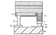
まず基板1上に少なくともn型窒化物半導体層、活性層、p型窒化物半導体層を有する窒化物半導体20を成長させる。その後、p型窒化物半導体層上に前記p電極10を形成する。p電極を矩形状や縞状、正方形、格子状、ドット状、菱形、平行四辺形、メッシュ形状、ストライプ形状、網目状、格子状の1つから複数に分岐した枝状等にパターン形成することで光の取り出し効率を上げることができる。好ましくは中央部には格子状、その外周を2つのL字で囲む形状とする。これによって大電流の投入が可能となる。
本実施の形態において、赤味を帯びた光を発光する蛍光体として、特に窒化物系蛍光体を使用するが、本発明においては、上述したYAG系蛍光体と赤色系の光を発光可能な蛍光体とを備える発光装置とすることも可能である。このような赤色系の光を発光可能な蛍光体は、波長が400〜600nmの光によって励起されて発光する蛍光体であり、例えば、Y2O2S:Eu、La2O2S:Eu、CaS:Eu、SrS:Eu、ZnS:Mn、ZnCdS:Ag,Al、ZnCdS:Cu,Al等が挙げられる。このようにYAG系蛍光体とともに赤色系の光を発光可能な蛍光体を使用することにより発光装置の演色性を向上させることが可能である。
以上のような蛍光体を選択することで、種々の発光波長を持った光取り出し効率の高い発光素子を得ることができる。
以下、図1に示す発光ダイオード素子を元に実施例1について説明する。
なお、本発明はこれに限定されるものではなく、p型窒化物半導体層に電極を形成する全ての窒化物半導体素子(レーザダイオード、太陽電池、光センサ、トランジスタ、パワーデバイスなど)に適用することができる。
実施例1において、図6Aに示すようにp電極10に開口部を形成する他は、同様にして発光ダイオード素子を得た。得られた素子は、If20mAにおいて、Vf3.5Vであり、p型窒化物半導体層と電極との良好なオーミック接触が得られた。発光出力は、電極の開口部を介して外部に光が取り出されるので実施例1と比較すると約20%増加していた。
実施例1において、p電極10として、NiとAuとを200オングストロームの膜厚で積層する他は、同様にして発光ダイオード素子を得た。得られた素子は、p電極10が透光性を有している。発光出力は、電極における光の吸収により実施例1と比較すると約20%減少していた。
[比較例2]
実施例1において、p電極10として、NiとPtとを200オングストロームの膜厚で積層する他は、同様にして発光ダイオード素子を得た。得られた素子は、p電極10が透光性を有している。発光出力は、電極における光の吸収により実施例1と比較すると約20%減少していた。
[比較例3]
実施例1において、p電極10として、Rhのみを400オングストロームの膜厚で積層する他は、同様にして発光ダイオード素子を得た。得られた素子は、p電極10が透光性を有している。発光出力は、電極における光の吸収により実施例1と比較すると同等であったが、Vfが約0.1V上昇した。
Claims (6)
- 少なくともn型窒化物半導体層とp型窒化物半導体層とを有する窒化物半導体素子において、前記p型窒化物半導体層に、少なくともロジウムとイリジウムとを含有する電極が形成されており、
前記電極は、前記p型窒化物半導体層に接して前記ロジウムが積層され、その上に前記イリジウムが積層された少なくとも2層構造を有し、
前記ロジウムの膜厚は10〜1000オングストロームであり、
前記電極は、前記ロジウムの上に前記イリジウムが積層された後に、400℃〜650℃の範囲においてアニーリングされていることを特徴とする窒化物半導体素子。 - 前記イリジウムの膜厚が10〜1000オングストロームであることを特徴とする請求項1に記載の窒化物半導体素子。
- 前記電極は、前記イリジウムの上にさらにPt、Ti、Zr、Hf、V、Nb、Ta、Mo、Wから選ばれる少なくとも1つが積層されてなることを特徴とする請求項1又は2に記載の窒化物半導体素子。
- 前記電極の上には、最上に金が積層されたパッド電極を有することを特徴とする請求項1乃至3のいずれかに記載の窒化物半導体素子。
- 前記2層構造全体の膜厚は、500〜1000オングストロームであることを特徴とする請求項1乃至4のいずれかに記載の窒化物半導体素子。
- 前記窒化物半導体素子は、基板側及び素子の端面側から光が取り出されることを特徴とする請求項1乃至5のいずれかに記載の窒化物半導体素子。
Priority Applications (2)
| Application Number | Priority Date | Filing Date | Title |
|---|---|---|---|
| JP2003300714A JP4507532B2 (ja) | 2002-08-27 | 2003-08-26 | 窒化物半導体素子 |
| US10/676,267 US6921928B2 (en) | 2002-08-27 | 2003-10-02 | Nitride semiconductor element |
Applications Claiming Priority (2)
| Application Number | Priority Date | Filing Date | Title |
|---|---|---|---|
| JP2002246573 | 2002-08-27 | ||
| JP2003300714A JP4507532B2 (ja) | 2002-08-27 | 2003-08-26 | 窒化物半導体素子 |
Publications (3)
| Publication Number | Publication Date |
|---|---|
| JP2004006991A JP2004006991A (ja) | 2004-01-08 |
| JP2004006991A5 JP2004006991A5 (ja) | 2006-10-12 |
| JP4507532B2 true JP4507532B2 (ja) | 2010-07-21 |
Family
ID=30447690
Family Applications (1)
| Application Number | Title | Priority Date | Filing Date |
|---|---|---|---|
| JP2003300714A Expired - Fee Related JP4507532B2 (ja) | 2002-08-27 | 2003-08-26 | 窒化物半導体素子 |
Country Status (2)
| Country | Link |
|---|---|
| US (1) | US6921928B2 (ja) |
| JP (1) | JP4507532B2 (ja) |
Families Citing this family (56)
| Publication number | Priority date | Publication date | Assignee | Title |
|---|---|---|---|---|
| CN100595938C (zh) * | 2002-08-01 | 2010-03-24 | 日亚化学工业株式会社 | 半导体发光元件及其制造方法、使用此的发光装置 |
| DE102004014940A1 (de) * | 2003-03-26 | 2004-10-21 | Kyocera Corp. | Halbleitervorrichtung, Verfahren zum Aufwachsen eines Nidridhalbleiters und Verfahren zur Herstellung einer Halbleitervorrichtung |
| US20050051781A1 (en) * | 2003-09-08 | 2005-03-10 | United Epitaxy Company, Ltd. | Light emitting diode and method of making the same |
| JP3767863B2 (ja) * | 2003-12-18 | 2006-04-19 | ローム株式会社 | 半導体発光素子およびその製法 |
| KR100586948B1 (ko) * | 2004-01-19 | 2006-06-07 | 삼성전기주식회사 | 질화물 반도체 발광소자 및 그 제조방법 |
| KR100482511B1 (ko) * | 2004-02-05 | 2005-04-14 | 에피밸리 주식회사 | Ⅲ-질화물계 반도체 발광소자 |
| US7611641B2 (en) * | 2004-02-20 | 2009-11-03 | Koninklijke Philips Electronics N.V. | Illumination system comprising a radiation source and a fluorescent material |
| JP2005277401A (ja) * | 2004-02-24 | 2005-10-06 | Showa Denko Kk | 窒化ガリウム系化合物半導体積層物およびその製造方法 |
| WO2005081329A1 (en) * | 2004-02-24 | 2005-09-01 | Showa Denko K.K. | Gallium nitride-based compound semiconductor multilayer structure and production method thereof |
| JP4670034B2 (ja) | 2004-03-12 | 2011-04-13 | 学校法人早稲田大学 | 電極を備えたGa2O3系半導体層 |
| US7462086B2 (en) * | 2004-04-21 | 2008-12-09 | Philips Lumileds Lighting Company, Llc | Phosphor for phosphor-converted semiconductor light emitting device |
| TWI242893B (en) * | 2004-05-07 | 2005-11-01 | Lite On Technology Corp | White light-emitting apparatus |
| JP2006229219A (ja) * | 2004-05-12 | 2006-08-31 | Showa Denko Kk | III族窒化物p型半導体およびその製造方法 |
| US7683391B2 (en) * | 2004-05-26 | 2010-03-23 | Lockheed Martin Corporation | UV emitting LED having mesa structure |
| US20050274971A1 (en) * | 2004-06-10 | 2005-12-15 | Pai-Hsiang Wang | Light emitting diode and method of making the same |
| JP4116985B2 (ja) * | 2004-07-26 | 2008-07-09 | 松下電器産業株式会社 | 発光装置 |
| WO2006028118A1 (ja) * | 2004-09-08 | 2006-03-16 | Rohm Co., Ltd | 半導体発光素子 |
| US7417220B2 (en) | 2004-09-09 | 2008-08-26 | Toyoda Gosei Co., Ltd. | Solid state device and light-emitting element |
| JP4721691B2 (ja) * | 2004-11-26 | 2011-07-13 | 京セラ株式会社 | 発光素子およびその発光素子を用いた照明装置 |
| US7307291B2 (en) * | 2005-01-22 | 2007-12-11 | Formosa Epitaxy Incorporation | Gallium-nitride based ultraviolet photo detector |
| JP4601464B2 (ja) * | 2005-03-10 | 2010-12-22 | 株式会社沖データ | 半導体装置、プリントヘッド、及びそれを用いた画像形成装置 |
| EP1868251A4 (en) * | 2005-04-08 | 2009-05-27 | Mitsubishi Chem Corp | SEMICONDUCTOR ELEMENT AND METHOD FOR MANUFACTURING THE SAME |
| JP5136765B2 (ja) * | 2005-05-02 | 2013-02-06 | 日亜化学工業株式会社 | 窒化物系半導体素子及びその製造方法 |
| JP5138873B2 (ja) | 2005-05-19 | 2013-02-06 | 日亜化学工業株式会社 | 窒化物半導体素子 |
| JP2006332258A (ja) * | 2005-05-25 | 2006-12-07 | Matsushita Electric Ind Co Ltd | 窒化物半導体装置及びその製造方法 |
| KR101041843B1 (ko) * | 2005-07-30 | 2011-06-17 | 삼성엘이디 주식회사 | 질화물계 화합물 반도체 발광소자 및 그 제조방법 |
| JP5025932B2 (ja) * | 2005-09-26 | 2012-09-12 | 昭和電工株式会社 | 窒化物半導体発光素子の製造方法 |
| WO2007081719A2 (en) | 2006-01-05 | 2007-07-19 | Illumitex, Inc. | Separate optical device for directing light from an led |
| US20070200119A1 (en) * | 2006-02-26 | 2007-08-30 | Yun-Li Li | Flip-chip led package and led chip |
| JP5232969B2 (ja) * | 2006-03-23 | 2013-07-10 | 豊田合成株式会社 | 窒化ガリウム系化合物半導体発光素子の製造方法 |
| US20070241351A1 (en) * | 2006-04-14 | 2007-10-18 | Applied Materials, Inc. | Double-sided nitride structures |
| JP2010506402A (ja) | 2006-10-02 | 2010-02-25 | イルミテックス, インコーポレイテッド | Ledのシステムおよび方法 |
| TWI338387B (en) * | 2007-05-28 | 2011-03-01 | Delta Electronics Inc | Current spreading layer with micro/nano structure, light-emitting diode apparatus and its manufacturing method |
| US8410510B2 (en) * | 2007-07-03 | 2013-04-02 | Nichia Corporation | Semiconductor light emitting device and method for fabricating the same |
| CN101939849A (zh) | 2008-02-08 | 2011-01-05 | 伊鲁米特克有限公司 | 用于发射器层成形的系统和方法 |
| KR101449035B1 (ko) * | 2008-04-30 | 2014-10-08 | 엘지이노텍 주식회사 | 반도체 발광소자 |
| TW201034256A (en) | 2008-12-11 | 2010-09-16 | Illumitex Inc | Systems and methods for packaging light-emitting diode devices |
| JP5078039B2 (ja) * | 2009-01-19 | 2012-11-21 | 学校法人早稲田大学 | Ga2O3系半導体素子及びGa2O3系半導体素子の製造方法 |
| US8449128B2 (en) | 2009-08-20 | 2013-05-28 | Illumitex, Inc. | System and method for a lens and phosphor layer |
| US8585253B2 (en) | 2009-08-20 | 2013-11-19 | Illumitex, Inc. | System and method for color mixing lens array |
| US10205059B2 (en) * | 2010-02-09 | 2019-02-12 | Epistar Corporation | Optoelectronic device and the manufacturing method thereof |
| US8927959B2 (en) | 2010-06-18 | 2015-01-06 | Sensor Electronic Technology, Inc. | Deep ultraviolet light emitting diode |
| US8907322B2 (en) * | 2010-06-18 | 2014-12-09 | Sensor Electronic Technology, Inc. | Deep ultraviolet light emitting diode |
| US9806226B2 (en) | 2010-06-18 | 2017-10-31 | Sensor Electronic Technology, Inc. | Deep ultraviolet light emitting diode |
| JP5517882B2 (ja) * | 2010-10-20 | 2014-06-11 | シャープ株式会社 | 窒化物半導体発光素子 |
| JP5652234B2 (ja) * | 2011-02-07 | 2015-01-14 | 日亜化学工業株式会社 | 半導体発光素子 |
| JP5869961B2 (ja) * | 2012-05-28 | 2016-02-24 | 株式会社東芝 | 半導体発光装置 |
| JP2013251493A (ja) * | 2012-06-04 | 2013-12-12 | Toshiba Corp | 素子モジュール |
| KR102005236B1 (ko) * | 2012-07-05 | 2019-07-31 | 삼성전자주식회사 | 반사 전극 형성을 위한 콘택층을 포함하는 반도체 발광 소자 |
| DE102012107384A1 (de) | 2012-08-10 | 2014-02-13 | Osram Opto Semiconductors Gmbh | Optoelektronisches Halbleiterbauelement und Verfahren zum Herstellen eines Spiegelbereichs auf einem Halbleiterkörper |
| DE102012108883A1 (de) * | 2012-09-20 | 2014-03-20 | Osram Opto Semiconductors Gmbh | Optoelektronischer Halbleiterchip und Verfahren zur Herstellung von optoelektronischen Halbleiterchips |
| US9419194B2 (en) | 2013-08-13 | 2016-08-16 | Palo Alto Research Center Incorporated | Transparent electron blocking hole transporting layer |
| TWI514628B (zh) | 2013-10-24 | 2015-12-21 | Lextar Electronics Corp | 電極結構與具有電極結構的發光二極體結構 |
| TWI625868B (zh) * | 2014-07-03 | 2018-06-01 | 晶元光電股份有限公司 | 光電元件及其製造方法 |
| JP2016062911A (ja) * | 2014-09-12 | 2016-04-25 | 株式会社東芝 | 半導体発光装置 |
| US20170104135A1 (en) * | 2015-10-13 | 2017-04-13 | Sensor Electronic Technology, Inc. | Light Emitting Diode Mounting Structure |
Citations (9)
| Publication number | Priority date | Publication date | Assignee | Title |
|---|---|---|---|---|
| JPH06204887A (ja) * | 1992-12-30 | 1994-07-22 | Casio Comput Co Ltd | データ圧縮伸張装置 |
| JPH10247747A (ja) * | 1997-03-05 | 1998-09-14 | Toshiba Corp | 半導体発光素子およびその製造方法 |
| JPH10335705A (ja) * | 1997-05-28 | 1998-12-18 | Nichia Chem Ind Ltd | 窒化ガリウム系化合物半導体素子及びその製造方法 |
| JPH11204887A (ja) * | 1998-01-19 | 1999-07-30 | Toshiba Corp | 低抵抗電極を有する半導体装置 |
| JP2000012899A (ja) * | 1998-06-17 | 2000-01-14 | Nichia Chem Ind Ltd | 窒化物半導体素子の製造方法 |
| JP2000183400A (ja) * | 1998-12-17 | 2000-06-30 | Toyoda Gosei Co Ltd | Iii族窒化物系化合物半導体発光素子 |
| JP2001168392A (ja) * | 1999-12-10 | 2001-06-22 | Stanley Electric Co Ltd | 半導体素子及びその製造方法 |
| JP2001345477A (ja) * | 2000-06-01 | 2001-12-14 | Matsushita Electric Ind Co Ltd | 窒化ガリウム系化合物半導体発光素子 |
| JP2002164575A (ja) * | 2000-11-27 | 2002-06-07 | Nichia Chem Ind Ltd | 窒化物半導体発光素子 |
Family Cites Families (14)
| Publication number | Priority date | Publication date | Assignee | Title |
|---|---|---|---|---|
| US5807774A (en) * | 1996-12-06 | 1998-09-15 | Sharp Kabushiki Kaisha | Simple method of fabricating ferroelectric capacitors |
| JP3365607B2 (ja) * | 1997-04-25 | 2003-01-14 | シャープ株式会社 | GaN系化合物半導体装置及びその製造方法 |
| US6168873B1 (en) * | 1997-05-29 | 2001-01-02 | Canon Kabushiki Kaisha | Electrode substrate and recording medium |
| JP4183299B2 (ja) | 1998-03-25 | 2008-11-19 | 株式会社東芝 | 窒化ガリウム系化合物半導体発光素子 |
| US6284654B1 (en) * | 1998-04-16 | 2001-09-04 | Advanced Technology Materials, Inc. | Chemical vapor deposition process for fabrication of hybrid electrodes |
| US6139780A (en) * | 1998-05-28 | 2000-10-31 | Sharp Kabushiki Kaisha | Dynamic random access memories with dielectric compositions stable to reduction |
| JP2000299528A (ja) | 1999-04-12 | 2000-10-24 | Nec Corp | 半導体レーザおよびその製造方法 |
| TW454330B (en) * | 1999-05-26 | 2001-09-11 | Matsushita Electronics Corp | Semiconductor apparatus and its manufacturing method |
| JP2001053339A (ja) * | 1999-08-11 | 2001-02-23 | Toshiba Corp | 半導体発光素子およびその製造方法 |
| JP4470262B2 (ja) * | 1999-09-07 | 2010-06-02 | オルガノ株式会社 | イオンクロマトグラフィー用カラム充填剤 |
| JP2001189430A (ja) * | 1999-12-28 | 2001-07-10 | Toshiba Corp | 強誘電体キャパシタ |
| IL151192A0 (en) * | 2000-02-16 | 2003-04-10 | Nichia Corp | Nitride semiconductor laser device |
| US6660577B2 (en) * | 2002-02-23 | 2003-12-09 | Taiwan Semiconductor Manufacturing Co. Ltd | Method for fabricating metal gates in deep sub-micron devices |
| JP2004014725A (ja) * | 2002-06-06 | 2004-01-15 | Toyoda Gosei Co Ltd | 半導体発光素子 |
-
2003
- 2003-08-26 JP JP2003300714A patent/JP4507532B2/ja not_active Expired - Fee Related
- 2003-10-02 US US10/676,267 patent/US6921928B2/en not_active Expired - Lifetime
Patent Citations (9)
| Publication number | Priority date | Publication date | Assignee | Title |
|---|---|---|---|---|
| JPH06204887A (ja) * | 1992-12-30 | 1994-07-22 | Casio Comput Co Ltd | データ圧縮伸張装置 |
| JPH10247747A (ja) * | 1997-03-05 | 1998-09-14 | Toshiba Corp | 半導体発光素子およびその製造方法 |
| JPH10335705A (ja) * | 1997-05-28 | 1998-12-18 | Nichia Chem Ind Ltd | 窒化ガリウム系化合物半導体素子及びその製造方法 |
| JPH11204887A (ja) * | 1998-01-19 | 1999-07-30 | Toshiba Corp | 低抵抗電極を有する半導体装置 |
| JP2000012899A (ja) * | 1998-06-17 | 2000-01-14 | Nichia Chem Ind Ltd | 窒化物半導体素子の製造方法 |
| JP2000183400A (ja) * | 1998-12-17 | 2000-06-30 | Toyoda Gosei Co Ltd | Iii族窒化物系化合物半導体発光素子 |
| JP2001168392A (ja) * | 1999-12-10 | 2001-06-22 | Stanley Electric Co Ltd | 半導体素子及びその製造方法 |
| JP2001345477A (ja) * | 2000-06-01 | 2001-12-14 | Matsushita Electric Ind Co Ltd | 窒化ガリウム系化合物半導体発光素子 |
| JP2002164575A (ja) * | 2000-11-27 | 2002-06-07 | Nichia Chem Ind Ltd | 窒化物半導体発光素子 |
Also Published As
| Publication number | Publication date |
|---|---|
| US6921928B2 (en) | 2005-07-26 |
| US20040195579A1 (en) | 2004-10-07 |
| JP2004006991A (ja) | 2004-01-08 |
Similar Documents
| Publication | Publication Date | Title |
|---|---|---|
| JP4507532B2 (ja) | 窒化物半導体素子 | |
| JP4572597B2 (ja) | 窒化物半導体素子 | |
| JP4325232B2 (ja) | 窒化物半導体素子 | |
| KR100909733B1 (ko) | 지지기판을 갖는 질화물 반도체소자 및 그 제조방법 | |
| JP4378070B2 (ja) | 窒化物半導体素子 | |
| JP5055678B2 (ja) | 窒化物半導体発光素子 | |
| JP3244010B2 (ja) | 周縁に電極を有する発光ダイオード | |
| JP4507594B2 (ja) | 半導体発光素子 | |
| JP3456413B2 (ja) | 窒化物半導体の成長方法及び窒化物半導体素子 | |
| JP2009049267A (ja) | 半導体発光素子及びその製造方法 | |
| JP3921989B2 (ja) | 半導体発光素子 | |
| JP2005259970A (ja) | 半導体発光素子 | |
| JP5077068B2 (ja) | 窒化物半導体素子及びその製造方法 | |
| JP5557649B2 (ja) | 発光ダイオード、発光ダイオードランプ及び照明装置 | |
| JP3301601B2 (ja) | 窒化物半導体発光素子 | |
| JP5586371B2 (ja) | 発光ダイオード、発光ダイオードランプ及び照明装置 | |
| US20130134390A1 (en) | Light-emitting diode, light-emitting diode lamp, and illumination device | |
| JP3847000B2 (ja) | 窒化物半導体基板上に活性層を備えた窒化物半導体層を有する窒化物半導体素子及びその成長方法 | |
| KR20140013249A (ko) | 자외선 발광 소자 및 발광 소자 패키지 | |
| JPH118410A (ja) | n型窒化物半導体の電極 | |
| JP4543621B2 (ja) | 窒化物半導体素子および窒化物半導体素子の製造方法 | |
| JP5557648B2 (ja) | 発光ダイオード、発光ダイオードランプ及び照明装置 | |
| US20230395754A1 (en) | Contact structures in light-emitting diode chips for reduced voiding of bonding metals | |
| JP3941464B2 (ja) | 窒化物半導体発光素子の製造方法 | |
| JPH10270755A (ja) | 窒化物半導体素子 |
Legal Events
| Date | Code | Title | Description |
|---|---|---|---|
| A521 | Request for written amendment filed |
Free format text: JAPANESE INTERMEDIATE CODE: A523 Effective date: 20060828 |
|
| A621 | Written request for application examination |
Free format text: JAPANESE INTERMEDIATE CODE: A621 Effective date: 20060828 |
|
| A131 | Notification of reasons for refusal |
Free format text: JAPANESE INTERMEDIATE CODE: A131 Effective date: 20090714 |
|
| A977 | Report on retrieval |
Free format text: JAPANESE INTERMEDIATE CODE: A971007 Effective date: 20090714 |
|
| A521 | Request for written amendment filed |
Free format text: JAPANESE INTERMEDIATE CODE: A523 Effective date: 20090904 |
|
| A02 | Decision of refusal |
Free format text: JAPANESE INTERMEDIATE CODE: A02 Effective date: 20091215 |
|
| A521 | Request for written amendment filed |
Free format text: JAPANESE INTERMEDIATE CODE: A523 Effective date: 20100303 |
|
| A911 | Transfer to examiner for re-examination before appeal (zenchi) |
Free format text: JAPANESE INTERMEDIATE CODE: A911 Effective date: 20100323 |
|
| TRDD | Decision of grant or rejection written | ||
| A01 | Written decision to grant a patent or to grant a registration (utility model) |
Free format text: JAPANESE INTERMEDIATE CODE: A01 Effective date: 20100413 |
|
| A01 | Written decision to grant a patent or to grant a registration (utility model) |
Free format text: JAPANESE INTERMEDIATE CODE: A01 |
|
| A61 | First payment of annual fees (during grant procedure) |
Free format text: JAPANESE INTERMEDIATE CODE: A61 Effective date: 20100426 |
|
| FPAY | Renewal fee payment (event date is renewal date of database) |
Free format text: PAYMENT UNTIL: 20130514 Year of fee payment: 3 |
|
| R150 | Certificate of patent or registration of utility model |
Ref document number: 4507532 Country of ref document: JP Free format text: JAPANESE INTERMEDIATE CODE: R150 Free format text: JAPANESE INTERMEDIATE CODE: R150 |
|
| FPAY | Renewal fee payment (event date is renewal date of database) |
Free format text: PAYMENT UNTIL: 20130514 Year of fee payment: 3 |
|
| FPAY | Renewal fee payment (event date is renewal date of database) |
Free format text: PAYMENT UNTIL: 20130514 Year of fee payment: 3 |
|
| FPAY | Renewal fee payment (event date is renewal date of database) |
Free format text: PAYMENT UNTIL: 20140514 Year of fee payment: 4 |
|
| R250 | Receipt of annual fees |
Free format text: JAPANESE INTERMEDIATE CODE: R250 |
|
| R250 | Receipt of annual fees |
Free format text: JAPANESE INTERMEDIATE CODE: R250 |
|
| R250 | Receipt of annual fees |
Free format text: JAPANESE INTERMEDIATE CODE: R250 |
|
| R250 | Receipt of annual fees |
Free format text: JAPANESE INTERMEDIATE CODE: R250 |
|
| R250 | Receipt of annual fees |
Free format text: JAPANESE INTERMEDIATE CODE: R250 |
|
| R250 | Receipt of annual fees |
Free format text: JAPANESE INTERMEDIATE CODE: R250 |
|
| R250 | Receipt of annual fees |
Free format text: JAPANESE INTERMEDIATE CODE: R250 |
|
| R250 | Receipt of annual fees |
Free format text: JAPANESE INTERMEDIATE CODE: R250 |
|
| R250 | Receipt of annual fees |
Free format text: JAPANESE INTERMEDIATE CODE: R250 |
|
| LAPS | Cancellation because of no payment of annual fees |